Device Applications of Synthetic Topological Insulator Nanostructures


State Key Laboratory of ASIC and System, School of Microelectronics, Fudan University, Shanghai 200433, China
*
Author to whom correspondence should be addressed.
Electronics 2018, 7(10), 225; https://0-doi-org.brum.beds.ac.uk/10.3390/electronics7100225
Submission received: 31 August 2018
/
Revised: 22 September 2018
/
Accepted: 26 September 2018
/
Published: 1 October 2018
(This article belongs to the Special Issue Nanoelectronic Materials, Devices and Modeling)
Abstract
:This review briefly describes the development of synthetic topological insulator materials in the application of advanced electronic devices. As a new class of quantum matter, topological insulators with insulating bulk and conducting surface states have attracted attention in more and more research fields other than condensed matter physics due to their intrinsic physical properties, which provides an excellent basis for novel nanoelectronic, optoelectronic, and spintronic device applications. In comparison to the mechanically exfoliated samples, the newly emerging topological insulator nanostructures prepared with various synthetical approaches are more intriguing because the conduction contribution of the surface states can be significantly enhanced due to the larger surface-to-volume ratio, better manifesting the unique properties of the gapless surface states. So far, these synthetic topological insulator nanostructures have been implemented in different electrically accessible device platforms via electrical, magnetic and optical characterizations for material investigations and device applications, which will be introduced in this review.
1. Introduction
In the past century, fundamental scientists and physicists have never stopped searching for new elementary particles. Instead of dealing with the atoms and electrons that were found centuries ago, there has been a growing interest in condensed matter physics in the formation of a new state of matter by putting the fundamental elements together. Other than the conventional states of matter such as conductors, insulators, semiconductors, superconductors and magnets, microcosmic mechanisms and quantum states of emerging states of matter are becoming more attractive with the boost of observation techniques and characterization capabilities. Since the first discovery of the quantum Hall (QH) state by Klitzing et al. in 1980 [1] which describes the electric current flow along the edges of a two-dimensional (2D) sample with insulating bulk, great effort has been made to seek the origin and manipulate such quantum state that is topologically different from all known states of matter.
The topological insulator is a newly discovered electronic phase which has insulating bulk and conducting surface [2,3,4]. Topological insulator is different from superconductors and magnets in that it has a topological order which is protected by time-reversal symmetry. These properties make it very attractive to realize high-mobility and non-dissipative electrical transmission. More interestingly, unlike the QH state, which requires the presence of a strong magnetic field, topological insulators can be observed without magnetic field. Instead, the spin-orbit coupling with heavy elements such as Hg and Bi induces magnetic field during the electron movement in 2D topological insulators. This is known as the quantum spin Hall (QSH) state, which was first experimentally observed in HgTe quantum wells in 2006 [5,6]. The three-dimensional (3D) topological insulator was predicted in BixSb1−x alloys in 2007, and shortly, binary chalcogenide compounds with simpler structure such as Bi2Se3, Bi2Te3, and Sb2Te3 were predicted as 3D topological insulators, which were further confirmed by angle-resolved photoemission spectroscopy (ARPES) and scanning tunneling microscopic (STM) measurements [4,7].
So far, 3D topological insulators have been widely explored and studied. However, the experimental realization of the prediction and applications of 3D topological insulators still remain elusive largely due to the interference from the conduction contribution from the bulk in small bandgap semiconductor. In recent years, 3D topological insulator nanostructures with thickness shrinking down to nanoscale while retaining the 3D topological insulator characteristics and stoichiometry have aroused more and more attention because of the large surface-to-volume ratio highlighting the surface conduction. These topological insulator nanostructures have provided excellent platforms for creative and innovative research, and have great potential for future device applications. Benefiting from quintuple layer structure of typical topological insulators such as Bi2Te3 and Bi2Se3, mechanical exfoliation similar to that used on graphene was first tested to fabricate simple yet low-cost topological insulator devices [8]. Significant progress has been achieved in the understanding and applications of topological insulators. For example, a magnetotransport measurement on the exfoliated Bi2Te3 device suggested that the 2D conduction channels originate from the surface states in the 3D topological insulators [9], and the coupling between the top and bottom surface states can result in an energy barrier close to the bulk bandgap demonstrated by the insulating behavior in exfoliated Bi2Se3 FET device [10]. In addition, optoelectronic properties of the exfoliated topological insulators have also been characterized. The spin direction of the electrons on the surface states of the exfoliated Bi2Se3 flake have been confirmed to be perpendicular to the electron movement, and it can be manipulated by shedding circular polarized light [11].
Although mechanical exfoliation has made the preparation of topological insulator samples easier with simple process and low cost, the challenge for realizing state-of-the-art device and manipulating the surface states of the exfoliated flakes still lies in minimizing the bulk conduction, which is basically originated from the chalcogen vacancies or anti-site defects. Furthermore, the low yield and random nature of the exfoliated flakes also make this method not suitable for large-scale fabrication and device integration. Up to now, various synthetic approaches to grow topological insulator nanostructures have been studied and developed, enabling more delicate devices while maintaining high surface-to-volume ratio. In this paper, we review the development of synthetic approaches for topological insulators nanostructures and their applications in novel nanoelectronic, spintronic and optoelectronic devices.
2. Synthesis Approaches
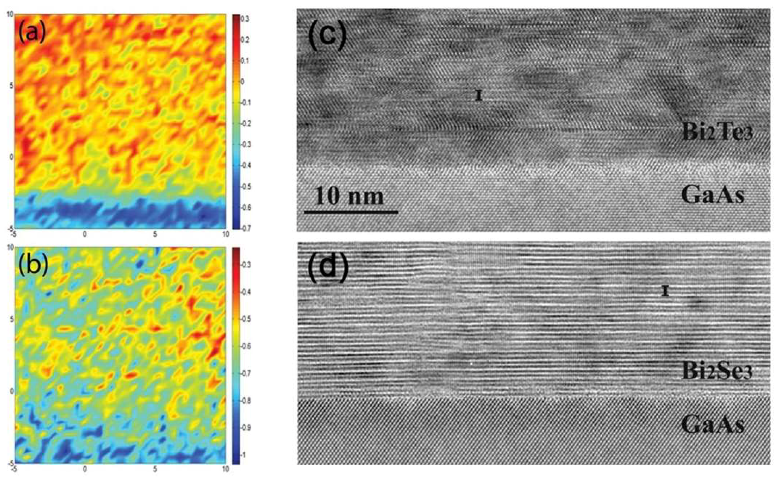
Although most current experimental research based on topological insulator still focuses on the surface states of thin films prepared by mechanical exfoliation from bulk material, various physical and chemical approaches to synthesize topological insulator nanostructures have been widely investigated. Molecular beam epitaxy (MBE) is one of the earliest synthetic methods to grow high-quality topological insulator thin films. Nominally stoichiometric single crystal thin film can be easily prepared by MBE, and more significantly, MBE deposition of topological insulator is based on a growth unit of one quintuple layer, with both physical and chemical reaction involved in the process. Although high vacuum environment is required during MBE deposition to allow the direct injection of atom or molecular beam onto the single crystal substrate, the synthesized films usually have good crystal integrity, precise composition and excellent large-scale uniformity. It has been demonstrated that the topological features of MBE-grown thin films start to appear from the thickness of 2 quintuple layers due to the weaker inter-surface coupling between the top and bottom surface as compared with 1 quintuple layer film [12]. In 2009, Zhang et al. reported the direct observation of quantum interference by the surface states on the MBE-grown Bi2Te3 thin film [13]. The high-quality single crystal Bi2Te3 film limited the nonuniform morphology, and the atomically flat film has been demonstrated to be a good platform to study the scattering of the topologically non-trivial surface states which are quantum mechanically protected by the time-reversal symmetry confirmed by the imaging of standing waves of the surface states using STM [13]. In 2012, Liu et al. synthesized Bi2Te3, Bi2Se3 films and their alloys on GaAs (001) substrates by using MBE [14]. Reflection high-energy electron diffraction (RHEED), atomic force microscopy (AFM), X-ray diffraction (XRD), high-resolution transmission electron microscopy (HRTEM), Raman spectroscopy and mapping characterizations have been used to examine the topological insulator thin film qualities. As shown in Figure 1a and Figure 2b, the Raman mapping patterns suggest that the position difference of the E2g Raman peaks are less than 1 cm− within a scan area of 15 μm × 15 μm, indicating good film uniformity in such a relatively small area. Figure 1c,d show the HRTEM images of the cross section of the grown topological insulator films on GaAs (001) substrate. Clear layered crystal features have been observed indicating good crystallinity [14]. However, quite few local and extended defects can also be observed which might be due to the instable growth process, and the imperfect interface between the topological insulator and the GaAs substrate is owing to the symmetry mismatch between the hexagonal lattice of Bi2Te3/Bi2Se3 and the cubic symmetry of GaAs (001) surface. Nevertheless, the topological insulator films synthesized by MBE is still of high crystalline quality, and further improvement of the interface can be expected through effective substrate engineering.
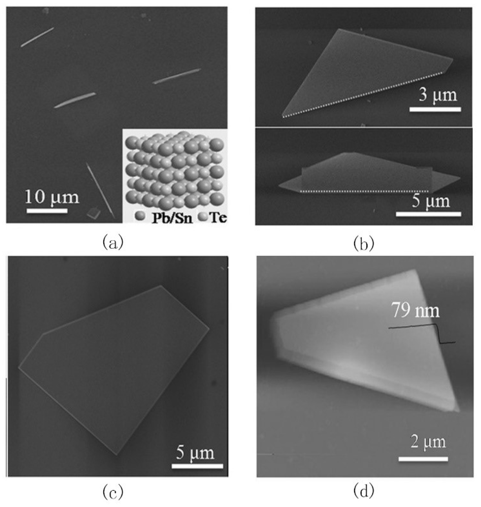
Referring to the MBE method, 3D topological insulators in planar geometry have been explored extensively using different synthetic methods. Chemical vapor deposition (CVD) is one of the most commonly used approach to grow topological insulator thin films in recent years. In a CVD process, chemical reactant evaporates and is gas-transferred to the targeted surface where chemical reaction occurs generating desired film materials. CVD is advantageous in fast-speed and large-area synthesis, and more importantly, the deposition can usually be carried out at low temperature which makes it very attractive in electronic device fabrication and integration compatible with current semiconductor technology. In 2016, Wang et al. reported the synthesis of ultra-large Pb1−xSnxTe topological insulator nanoplates by using low-cost and efficient CVD process [15]. The prominent characteristic of topological surface transport indicated that these nanoplates can be great candidates for low-dissipation transistors. The angle and temperature dependence of the magneto-conductance revealed the 2D nature of the weak antilocalization effect in them [15]. Besides, as shown in Figure 2, the peculiar 2D geometry of obtained nanoplates which can be applied to functional devices lay a foundation for the investigation of mirror symmetry–induced topological surface transport properties [15]. Metal-organic chemical vapor deposition (MOCVD) is a derivative technique of conventional CVD and has been implemented in the synthesis of topological insulator thin films recently. MOCVD uses metal organic compounds and hydrides as source material and topological insulator single crystal compounds grow on the substrate in the way of gas phase epitaxy through thermal decomposition reaction. MOCVD can enable high-purity, high-uniformity, large-scale and repeatable films, as well as precise control over the film thickness. In 2014, Bendt et al. demonstrated the layer-by-layer growth of smooth Sb2Te3 films on c-oriented Al2O3 substrates using Et2Te2 and i-Pr3Sb as precursors [16]. The obtained high-quality films allowed for the measurement of the topological surface state for MOCVD grown Sb2Te3 by ARPES for the first time. The results illustrated the high-quality topological surface state which is even comparable to the optimized bulk single crystals Sb2Te3 films and detailed dispersions of the bulk valence band. In terms of electrical sheet resistivity, the characteristic of increasing monotonically with rising temperature was also found [16].
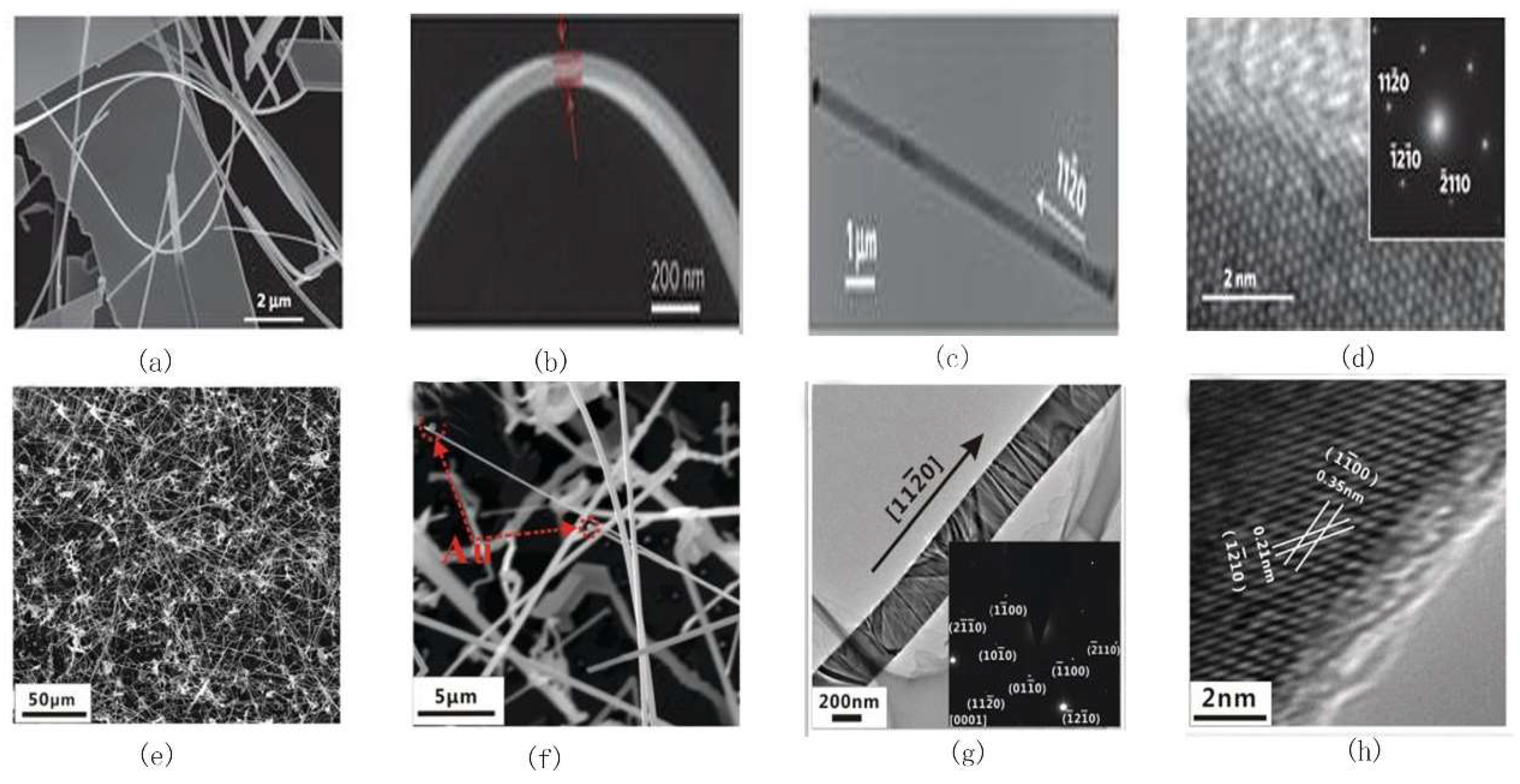
In addition to the topological insulator thin films, non-planar topological insulator nanostructures with reduced sample size have also become more and more intriguing such as nanowires, nanoribbons, nanosheets, and so forth. These nanostructures are expected to significantly enhance the surface conduction by suppressing the contribution of bulk carriers with their large surface-to-volume ratio. Typically, the quasi-one-dimensional nanostructures are synthesized by following the catalytic vapor–liquid–solid (VLS) method which has been widely used on the synthesis of silicon nanowires [17,18]. Au nanoparticles are commonly used as catalyst to stimulate the growth of semiconductor nanowire or nanoribbon through the precipitation from the supersaturated Au/semiconductor alloy. In 2010, Peng et al. reported the quantum interference effect in Bi2Se3 nanoribbon grown by the Au-catalyzed VLS process [19]. The cross-sectional area of the nanoribbon is 6.6 × 10⁻¹⁵ m2, which is largely determined by the size of catalyst nanoparticle (Figure 3a–d). Due to the large surface-to-volume ratio, the bulk conduction has been greatly limited, better manifesting the quantum interference effects of the surface states. Furthermore, such catalytical synthesis of topological insulator nanostructures can be applied in the fabrication of various heterogeneous structures. In 2016, Liu et al. reported single-crystalline topological insulator Bi2Se3 nanowires synthesized via Au-catalyzed VLS method, as shown in Figure 3e–h, which were further transferred and used to fabricate high-performance Bi2Se3/Si heterostructure photodetectors. The photodetectors exhibited excellent optoelectronic properties which were attributed to the high crystal quality of the Bi2Se3 nanowires and the high build-in electric field at the Bi2Se3/Si heterostructure interface [20]. This further evidenced the great prospect of high-quality topological insulator nanowires synthesized by catalytic VLS method.
Despite the methods introduced above, other synthesis methods such as solvothermal synthesis have also been used to prepare topological insulator nanostructures. For example, Xiu et al. synthesized Bi2Te3 nanoribbons by heating the polyvinylpyrrolidone (PVP) solvent added with Bi2O3, Te and ethylenediamine tetraacetic acid (EDTA) powders [21]. However, such chemical approaches involving organic solvent usually include harvesting and multiple cleaning processes, which will inevitably introduce contaminates and deteriorate the surface condition of the synthesized nanostructure. Actually, the major bottleneck of the synthetical topological insulator materials still lies in the crystal properties, specifically the intrinsic defects such as S or Se vacancies and interstitial defects. These defects are responsible for the bulk conduction, and gas molecules can occupy these vacancies forming different types of doping if the topological insulator surface is not passivated or effectively protected [22]. As a result, a lot of attention has been paid to the optimization of the synthesis process and the device structure engineering for in-depth investigation on the material properties and device applications. The following section briefly introduces the device applications of synthetic topological insulator nanostructures, including field-effect transistors, optoelectronic devices, magnetoelectric devices and so forth.
3. Device Applications
3.1. Field-Effect Transistor
The field-effect transistor (FET), based on semiconductor nanostructures, has been regarded as one of the fundamental building blocks for future nanoelectronic device and circuit technologies. Topological insulator FET is also the critical device architecture for further optoelectronics and spintronics applications. Although a variety of FET devices based on exfoliated or MBE-grown topological insulator thin films have been fabricated [10,23,24,25,26,27], yet, up to now, high-performance topological insulator FET devices such as the analog of metal-oxide-semiconductor field-effect-transistor (MOSFET) have been rarely reported. For conventional Si-based MOSFET devices, the surface conduction of Si channel is protected by the thermal SiO2 with optimized inversion characteristics allowing for better transistor performance. Similarly, the gapless surface states of 3D topological insulators have protected and robust conduction properties which are derived from the intrinsic material properties. Considering the current wide use and preference of silicon over other semiconductors, the integration of topological insulator nanostructures as the conduction channel replacing silicon in MOSFETs will be very attractive in future nanoelectronic device and circuit technologies.
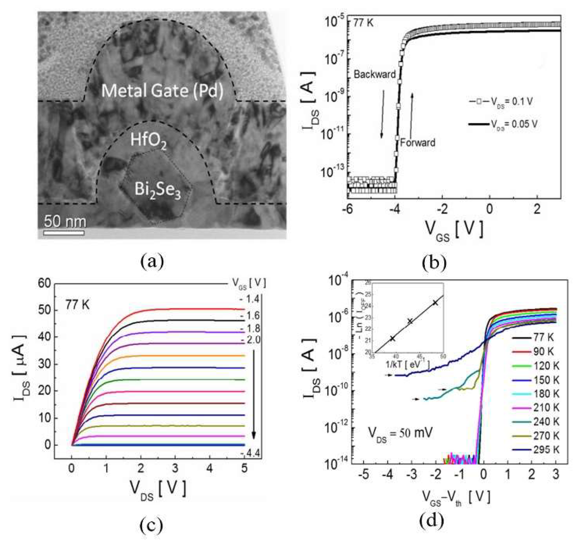
Synthetic topological insulator nanostructures, especially those in non-planar geometry usually have larger surface-to-volume ratio, which is very advantageous in highlighting the unique topological features of the metallic surface states. Furthermore, the integration of such topological insulator nanostructures in FET devices with tunable electrical gate control, the transport properties of the carriers in the bulk and on the surface can be further investigated with possible electrical manipulation. For example, in 2013, Zhu et al. synthesized high-quality single crystal Bi2Se3 nanowires by using the VLS mechanism, and integrated them in a high-performance FET device through a self-alignment process (Figure 4a) [28]. The Bi2Se3 nanowires were grown from pre-patterned Au catalyst, enabling the direct device fabrication without nanowire harvesting and manual positioning. This approach not only enables the batch fabrication of homogeneous nanowire FETs but also limits the steps in which contamination might be introduced degrading the topological insulator surface properties. Excellent electrical performance has been achieved, including very sharp turn-on, near-zero cutoff current, large On/Off ratio (over 108), and well-saturated output current (Figure 4b,c). As compared with the conventional Bi2Se3 thin film transistor, the Bi2Se3 nanowire FET exhibited much better electrostatic gate control and subthreshold behaviors [29]. More significantly, the surface states were protected by high-quality high-k dielectric, and the surrounding-gate device geometry has greatly enhanced the gate control over the channel allowing for the full depletion of electrons from the nanowire. Therefore, the temperature dependent off-state current is due to the thermal excitation across the bandgap of the bulk, which means that the off-state current obtained above 240 K is contributed from the bulk conduction [28]. On the other hand, the linear dependence of the saturation current on the over-threshold voltage suggests the drift current model instead of the diffusion current model such as in conventional MOSFET. Such metal-like behavior exactly indicates that the on-state current is dominated by the contribution from the metallic surface conduction. And due to the very sharp turn-on performance of the FET, the separation of the surface and bulk conduction can be effectively achieved within a range of a few volts (~2 V) of gate voltage [28]. Such controlling and manipulation over the surface conduction and insulating switch-off through electrical approaches open up a suite of potential application in novel nanoelectronic and spintronic devices.
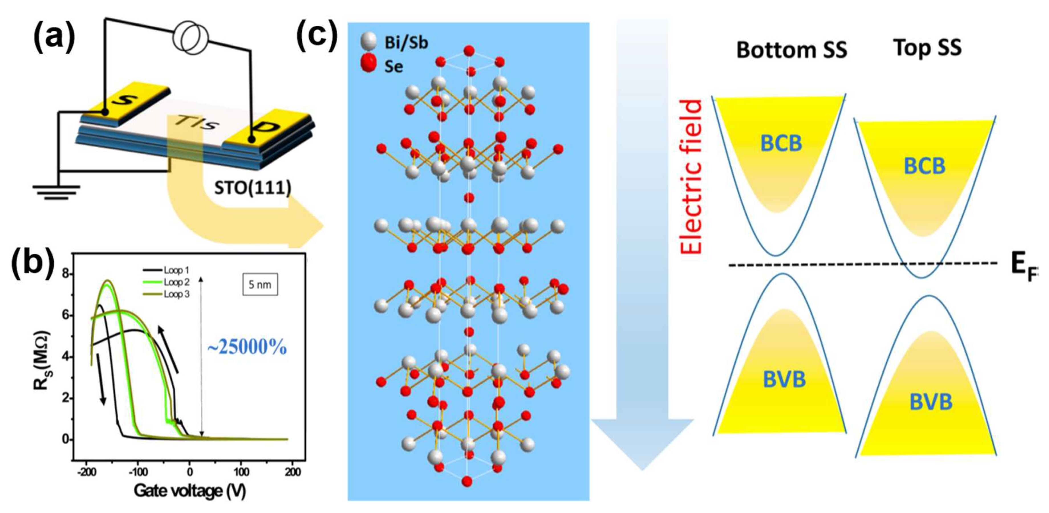
Although the synthetic nanowire and nanoribbon geometry can enable advanced device structure to demonstrate the conduction from bulk and surface separately by electrical gating, these nanostructures typically have a width (cross-sectional) of tens of nanometers. On the contrary, some unique and interesting topological phase transition such as that between a trivial insulator and a nontrivial topological phase can only be achieved in ultrathin systems, which however has not aroused sufficient attention. In 2017, Liu et al. reported ultrathin (Bi1−xSb)2Se3 field effect transistor with On/Off ratio reaching ~25,000% as shown in Figure 5a,b [30]. The ultrathin film (4.2 nm) was synthesized by MBE and the varying Sb doping level has been proved to be also effective in tuning the transport properties in FETs in addition to the electrical gating. In such a combined approach, a large On/Off ratio can be achieved by tuning the Fermi level in the regime around the surface gap. It has been reported that the top and bottom surface states in Bi2Se3-based topological insulators will be hybridized and will form a surface gap when the film thickness is below a critical value of 6 nm [30,31]. The In doping in Bi2Se3 can also tune the transport properties as well as enabling the phase transition from a nontrivial topological metal to a trivial band insulator (the so-called metal-insulator transition). Both the film thinning and Sb-doping enhance the electric field across the Bi2Se3 channel, and the spin-orbit coupling strength is reduced due to substitution of Bi with lighter Sb element. Eventually, the bulk bandgap is reduced and the penetration depth of the surface states is increased becoming comparable to the film thickness, leading to the opening of a surface gap [30]. This is the first experimental observation of a large On/Off ratio in ultrathin topological insulator FET.
As seen in most high-performance topological insulator FET research, the topological insulator surface channels are in direct contact with dielectric material in high-k/metal gate device structure. On the one hand, it is the prerequisite to implement the top gate FET geometry with topological insulator nanostructure as the channel. On the other hand, it has been found that topological insulator materials usually become heavily doped when exposed to air, so that the deposition of high-k dielectric can effectively prevent the N, O elements, and water molecules penetrating into the surface lattice. However, like other semiconductors without dangling bonds at the surface such as graphene and MoS2, it might be hard to realize a uniform deposition of high-k dielectric on the surface of topological insulator by using atomic layer deposition (ALD) [23,32,33]. This is because of the absence of dangling bonds on the surface resulting in no chemical adsorption and nucleation sites in the initial deposition cycles. Liu et al. have studied the ALD Al2O3 deposition on Bi2Te3 for a dual-gate FET device fabrication by testing different ALD parameters [34]. Different ALD precursors (trimethylaluminum (TMA) and H2O or TMA and O3) have been tested and compared. In the case of graphene and MoS2, in order to avoid the island or cluster morphology, some surface pretreatments are usually incorporated before the ALD deposition to generate nucleation sites for uniform dielectric deposition. Surprisingly, it is different for topological insulators as Liu et al. found that the surface is not as smooth as graphene which might be attributed to the oxidation of the Te-terminated surface by oxygen or water molecules. This oxidation facilitates the ALD process by generating nucleation sites for precursor adsorption [34]. However, as compared with the back-gate control, the top-gate control is less effective at the same electric field which is largely due to the degraded dielectric/Bi2Te3 interface during the ALD deposition. This is because of the introduced defects and impurities degrading the interface quality can act as trapping and de-trapping sites for the charge carriers leading to instable FET device performance. Nevertheless, like FETs based on other novel semiconductor materials such as transition metal dichalcogenides, more in-depth experimental and theoretical studies are still on-going to improve the high-k dielectric/topological insulator interface and optimize the ALD deposition process. In addition to the topological insulator/dielectric interface, the electron dynamics of topological insulator-based semiconductor-metal interface and interface engineering methods have also been investigated to provide reference for further device fabrications [35,36].
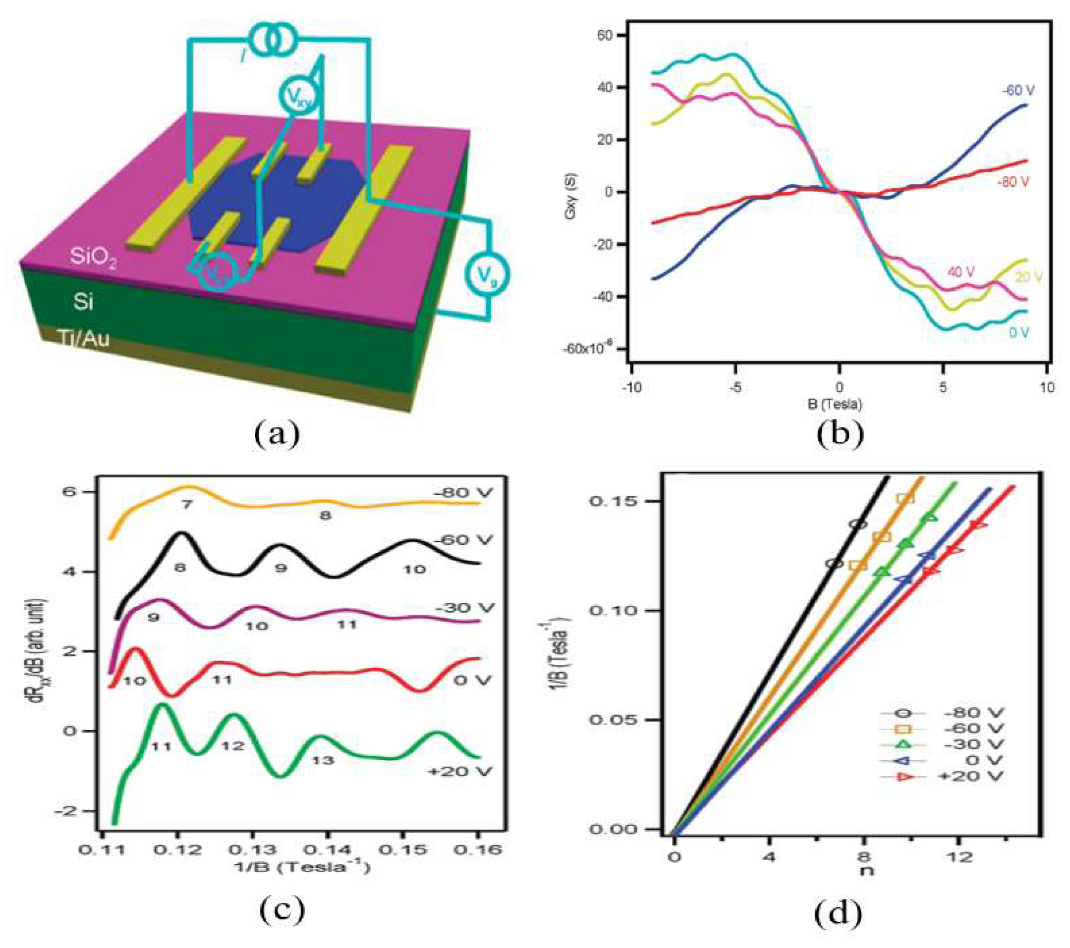
Similar to other novel semiconductors, the Fermi level in topological insulators can be effective tuned by constructing FET device and applying gate voltage [37,38,39,40,41]. In this way, the bulk carriers in topological insulators nanostructures can be easily depleted, achieving larger contribution from the surface conduction. However, sometimes the position of the Fermi level cannot be properly tuned only by using electrical gating to the same or the adjacent regime to the intrinsic Fermi level, because it might fall into the valence band under negative voltages. Elemental doping has been confirmed to be an effective approach to assist the manipulation of Fermi level in topological insulator nanostructures [42,43,44]. In 2012, Wang et al. reported the Na elemental doping in Bi2Te3 nanoplates synthesized by solvothermal method [45]. The ~0.8% Na doping was expected to tune the Fermi level of Bi2Te3 nanoplates toward the middle of the bandgap. By integrating such doped Bi2Te3 topological insulator nanoplates in a back-gate FET device (Figure 6a), the tuned Fermi level in the Bi2Te3 channel material enables the transition between different conduction types by using gate voltages. As shown in Figure 6b, the Hall measurement results indicated that the gate voltage can change the dominating conduction channels, and when the conduction contribution from the surface electrons and bulk electrons is larger than that from bulk holes, the Bi2Te3 FET exhibited n-type behavior. On the contrary, if the bulk holes dominated the conduction, p-type behavior was observed [45]. Moreover, through the magnetotransport measurement on the Na-doped Bi2Te3 nanoplate FET, distinct quantum interference effects under various gate voltage have been observed. As shown in Figure 6c,d, the frequency of the Shubnikov-de Hass (SdH) oscillation exhibited a clear increasing trend with increasing gate voltage, indicating higher Landau levels. The parameters estimated from the SdH oscillation such as the Fermi wavevector for different gate voltages also indicate that the oscillation is originated from the surface states [45]. Utilizing electrical gating to achieve the control and manipulation over the surface states of the intrinsic or doped topological insulator nanostructures has provided an efficient and effective approach to study the transport properties of the materials and dissipationless electronic and spintronic device applications.
It is worth mentioning here that synthetic topological insulator nanostructures have attracted more attention in recent years due to their high-quality single crystal nature and enhanced surface-to-volume ratio as compared with bulk materials. This has provided excellent geometries for probing the transport properties of the surface states, such as the research reported in References [19]. However, although these works took advantages of the geometry of the synthetic topological insulator nanostructures, there lacks effective gate control to further manifest the topological features of the surface states, which is very important to realize future electrically accessible devices. Up to now, full understanding over the transport properties of 3D topological insulator by interpreting the electrical behavior under various circumstances through careful device structure design and engineering has not been seen yet.
3.2. Optoelectronic Device
Optoelectronic devices can generate or sense light, or convert it into electric signal that can be processed by electronic devices and apparatus. Typical optoelectronic devices include lasers, light emitting diode (LED), photodetector, solar cell, and so forth. Up until now, various semiconductors have been studied extensively for different kinds of optoelectronic applications. For example, Si-based optoelectronic devices are advantageous in the CMOS compatibility which can be directed integrated on Si substrates. III–V compound-based optoelectronic devices are also attractive in the applications of optical fiber, infrared and visible LEDs and high efficiency solar cells. Novel 2D semiconductors such as MoS2 and black phosphorus are also interesting candidates in realizing ultra-scaled optoelectronic devices due to their 2D nature and thickness-depended band structure. On the other hand, topological insulators also have intrinsic attractive optical properties such as high bulk refractive index and broadband surface plasmon resonance. In addition, topological insulators usually have a narrow bandgap which can improve the conductivity and also enables high transparency in near-infrared frequency regime. The Dirac-like surface states of topological insulator can bring strong optical absorption, enabling high-performance broadband photodetection capabilities. It has been theoretically proposed that topological insulators can electrically response to light signals, due to their novel and intriguing quantum phase of matter with spin-polarized surface states. For example, this effect has been preliminarily characterized by the photo-induced quantum phase transitions between conventional insulator and topological insulators in 2D electronic system [46], as well as the generation of helicity-dependent direct current by circularly polarized light [47]. In 2012, Mclver et al. have experimentally observed a photocurrent which is originated from the topological helical Dirac fermions from an exfoliated Bi2Se3 thin flake [11]. More interestingly, the direction of the photocurrent can be reversed by reversing the helicity of the light. This is the first experimental demonstration of the circular and linear photogalvanic effects on topological insulators where the Rashba spin-split valence and conduction bands provide the asymmetric spin distribution. However, the observed polarization-dependent photocurrent always coexists with bulk photocurrent. This is because the depopulation of the Dirac cone using polarize light will generate bulk-like excited states. The contribution of photocurrent arising from the bulk can be expected to be eliminated by using samples with more insulating bulk and lower light energy. Nevertheless, the interference from the bulk state has been one of the major bottlenecks to further investigate the optoelectronic properties of the surface states in topological insulators.
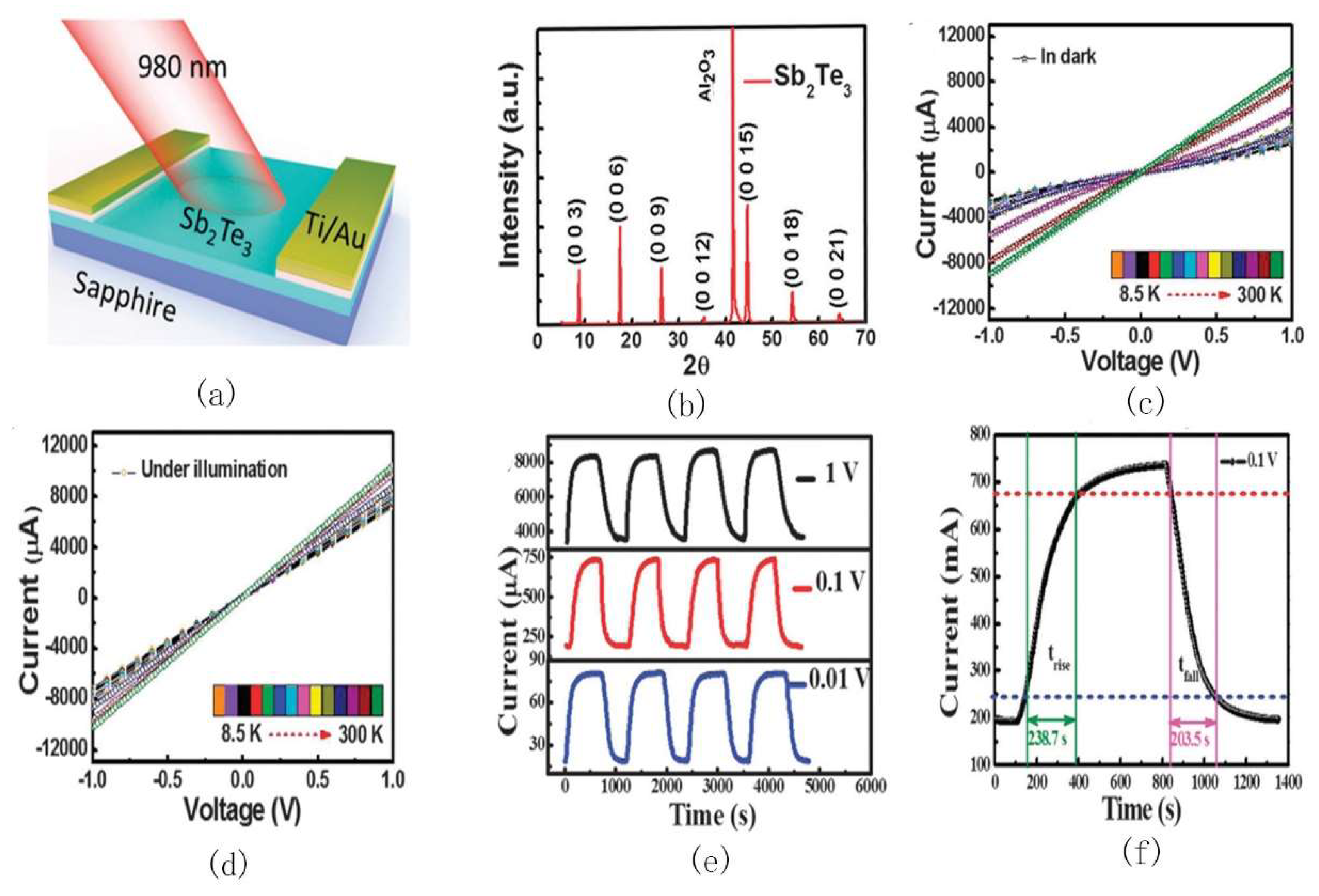
Synthetic topological insulator nanostructures have also been tested in various optoelectronic device structures to study the photo-sensing and photo-detecting properties of the surface states. For example, in 2015, Zheng et al. reported a near infrared light photodetector based on Sb2Te3 ultra-thin film synthesized by MBE [48]. As shown in Figure 7, they found that the Sb2Te3 photodetector was sensitive to 980 nm light illumination, and the responsivity was 21.7 A/W, which was much better than most reported topological insulator-based photodetectors. However, both bulk and surface states contributed to the photocurrent and responsivity, with possible dominating contribution from the bulk due to the electron-hole pairs generated by photons. The interesting finding is that the bulk and surface contribution exhibited different temperature dependent responsive behaviors with the bulk state has a higher responsivity at room temperature while the surface state has higher responsivity at lower temperature [48]. This can lead to novel photo-detecting applications in complicated environment. Another shortcoming of the topological insulator back-gate FET based photodetector lies in the relatively slow response speed (Figure 7f) which is largely due to the degradation of the exposed surface states without protection. Dangling bonds or absorbents can be generated and introduced on the surface acting as the trapping centers thus reducing the response speed. Nevertheless, the contribution from the surface states still confirms the formation of a spin-polarized electrical signal under the polarized light illumination, and the relatively high responsivity is due to the location of the Dirac point near the Fermi level in the topological insulator film [49]. In order to improve the immunity of the optoelectronic properties of topological insulator devices, surface passivation by the ALD deposition of high-k dielectric is a useful and straightforward approach. However, as described in the previous section, uniform formation of oxide film on the surface of topological insulator also involves the deterioration of the surface conditions due to the adsorption of oxygen or water. The oxidation of topological insulators such as Bi2Te3 can shift the Fermi level towards up or down with respect to the Dirac point leading to degradation of photoconductivity in optoelectronic devices. More theoretical and experimental work focusing on the surface passivation or device structure engineering are still necessary to rule out the factors from external ambient for more accurate evaluation of the optoelectronic properties of topological insulators.
An alternative approach to enhance the surface contribution of the photocurrent is to use non-planar synthetic topological insulator nanostructures with larger surface-to-volume ratio such as nanowires and nanoribbons. For example, very recently in 2017, broad spectral photodetection from ultra-violet to near-infra-red was reported based on a Bi2Te3 nanowire photodetector [50]. Device performance was compared between the exfoliated Bi2Te3 nanosheets and the Bi2Te3 nanowires which were fabricated by milling the nanosheet using focused ion beam (FIB). The nanosheets of Bi2Te3 exhibited ultra-high photoresponsivity of 74 A/W at 1550 nm. More significantly, the nanowires transformed by FIB milling showed about one order enhancement in photoresponsivity. It is worth to mention that the FIB fabrication of nanowires involves harsh exposure environment with inevitable Ga ions implantation and even sample deformation during the milling process. The enhancement in photoresponsivity is exactly due to the nano-confinement effects of topological insulator surface states and more electron-hole pair generation for effective incident photons. Further aging tests showed that the devices still have robust detectivity and photoconductivity even after a period of four months’ time. The above experimental results explicitly demonstrate the efficient carrier transport through the robust topological surface states which is resistant to material deformation and non-magnetic impurities. Promising improvement in topological insulator-based optoelectronic device can also be expected with future advanced synthetic nanomaterials and device engineering.
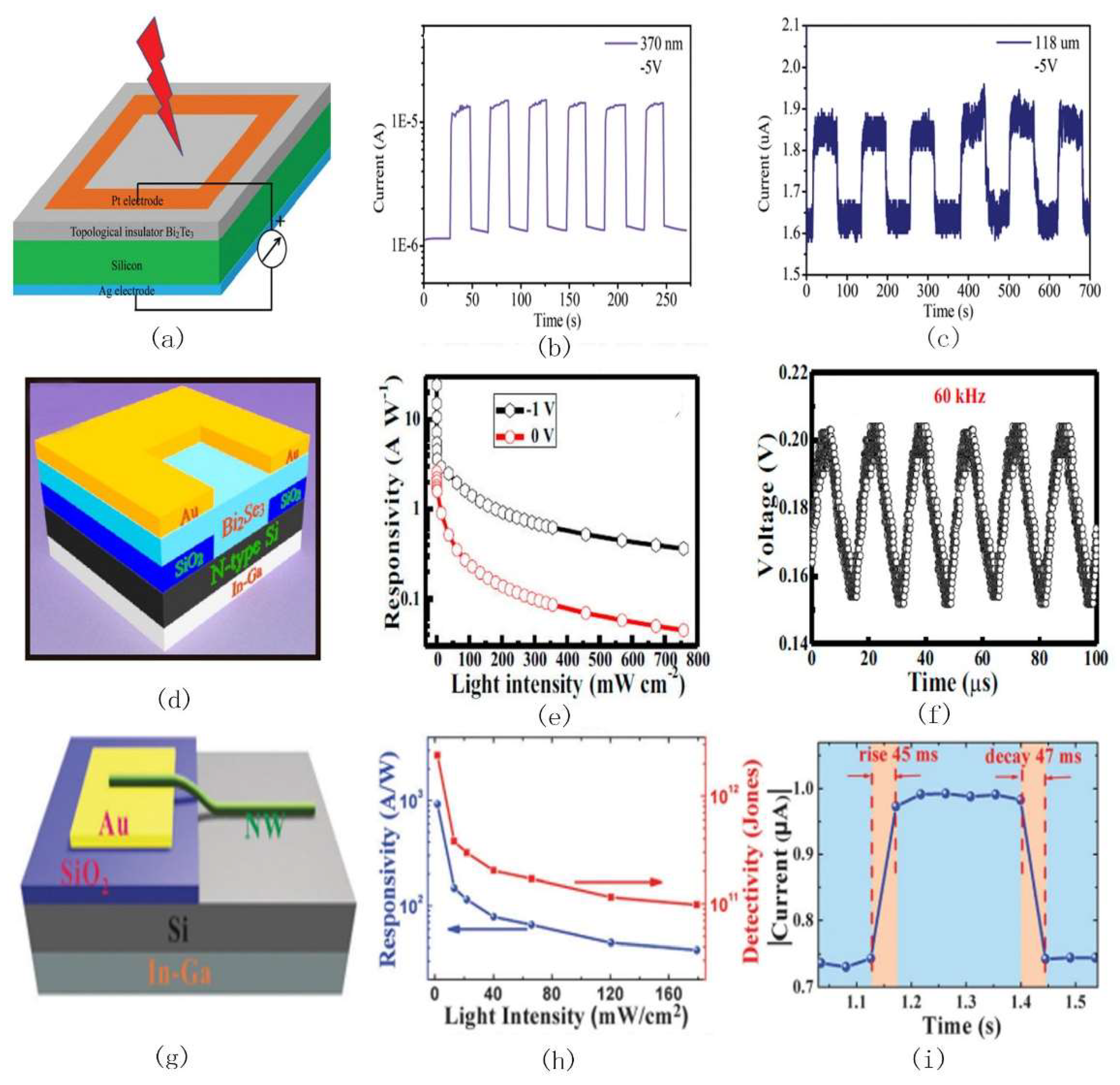
Another superiority of the synthetic nanostructures over the exfoliated flakes is the feasibility to fabricate high-quality topological insulator-based heterostructures [51,52,53,54,55]. The interface in the synthetic topological insulator-based heterostructure is much better than that of the exfoliated flake system. This is very helpful to enhance the effective generation and transfer of the photocarriers at the interface, enlarging the photocurrent without sacrificing the detecting spectral width. In 2015, Yao et al. reported a photodetector built with Bi2Te3/Si heterostructure which exhibited a prominent characteristic of ultra-broadband photodetection (370–118,000 nm) (Figure 8a–c) [56]. Besides, the responsivity of 1 A/W and detectivity of 2.5 × 1011 cm·Hz1/2·W−1 have been achieved as well as excellent device stability even after long-time high-energy exposure and acidic treatment. However, the Bi2Te3 thin film in this heterostructure device was deposited by using pulsed laser deposition (PLD) technique, which is not favorable in forming high-quality single-crystal films. The intrinsic topological surface states and the Bi2Te3/Si interface will be deteriorated in the as-synthesized polycrystalline Bi2Te3 film, degrading the photodetection performance. In 2016, Zhang et al. reported a high-performance Bi2Se3/Si heterostructure photodetector in which the single crystal Bi2Se3 was deposited by using CVD method, which is superior in forming high-quality single-crystal topological insulator samples as compared with PLD method [57]. As shown in Figure 8d–f, high light responsivity (24.28 A/W), high detectivity (4.39 × 1012 cm·Hz1/2·W−1) and fast response speed (microseconds approximately) have been obtained. Broadband detection was also realized (300–1100 nm). Comparing the two reported work above, the similar band structure of Bi2Te3 and Bi2Se3 topological insulators actually demonstrated the significance of the crystalline quality and resulted interface of topological insulator thin film in optimizing the optoelectronic characteristics by using different crystal synthesis approaches. Later in 2016, Liu et al. investigated the photodetector built with Bi2Se3 nanowire/Si heterostructure [20]. The Au-catalyzed Bi2Se3 nanowires were transferred on pre-patterned Si substrate area to form the heterostructure. As shown in Figure 8g–i, the device showed an extremely high responsivity reaching 103 A/W which is much higher than the above Bi2Se3/Si heterostructures [20]. In addition, a broad spectral ranging from 380 to 1310 nm and fast response speed of tens of milliseconds were also achieved. Such high performance was attributed to the superior nanowire quality, and the strong built-in electric field at the heterostructure interface which prohibited the recombining of electron-hole pairs. It should be mentioned here that the Bi2Se3/Si heterostructure was formed simply by stacking the nanowires on Si substrate, this is not beneficial to form a high-quality interface with least defects. Unfortunately, no ideal heterostructure such as Bi2Se3 nanowire/Si nanowire by using VLS synthesis has yet been reported.
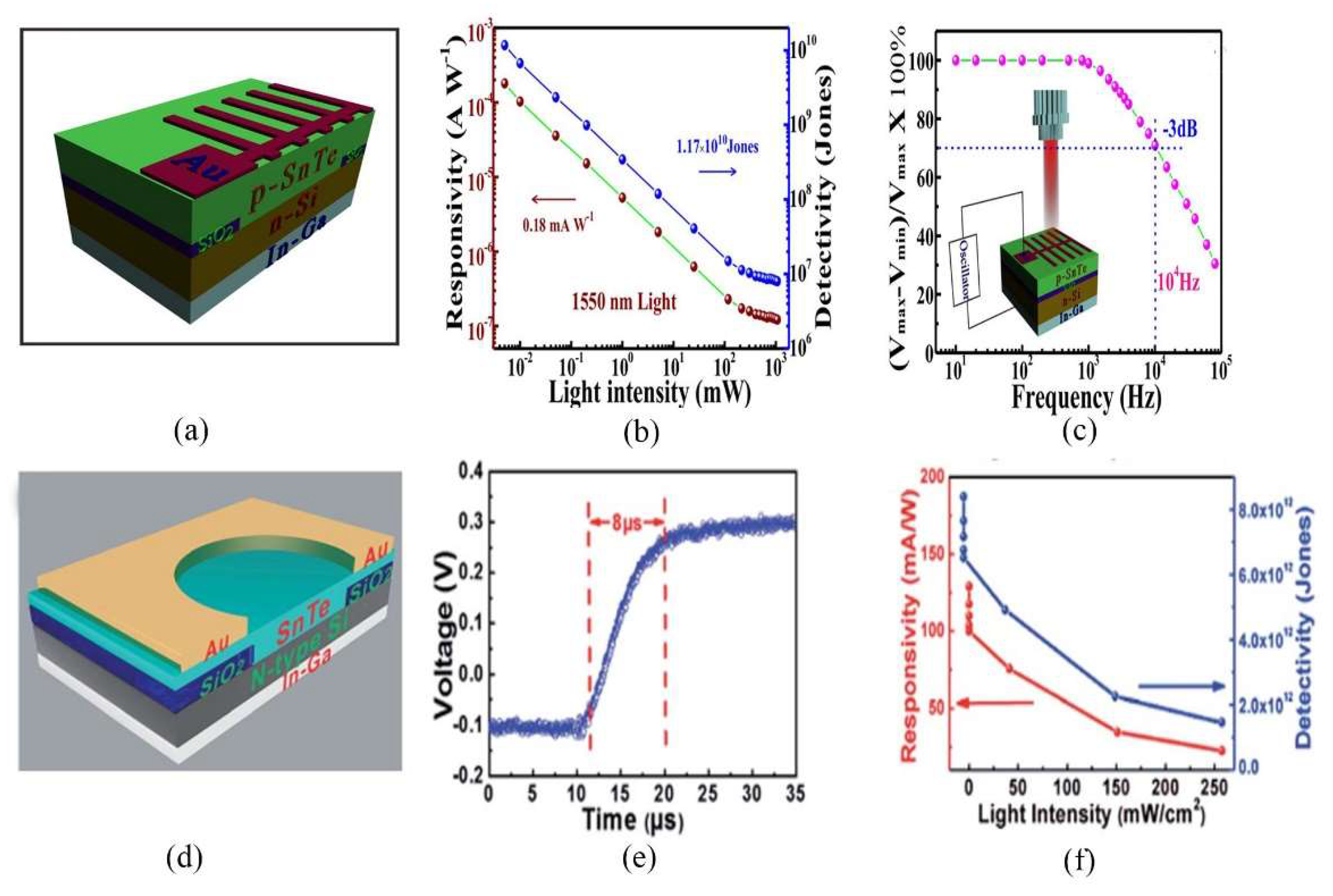
In 2017, Zhang et al. fabricated thin film-based SnTe/Si vertical heterostructure photodetectors with direct p-SnTe vapor deposition on n-Si surface. High-performance near-infrared detection has been achieved. With the assistance from the built-in electric field in SnTe/Si interface, the absorption efficiency and the separation of photogenerated carriers were greatly improved and the SnTe/Si heterostructure photodetector can have a responsivity of 2.36 AW−1, a high detectivity of 1.54 × 10¹⁴ Jones, and a large bandwidth of 104 Hz in the near-infrared wavelength, which were shown in Figure 9a–c [58]. Later in 2017, Gu et al. also adopted SnTe/Si heterostructures but by CVD method to fabricate photovoltaic detectors. This self-driven detector realized broadband detection (254 nm–1550 nm), ultrafast response speed (~8 μs) and high detectivity (8.4 × 10¹² Jones) as shown in Figure 9d–f [59]. Both work utilized SnTe as the p-type semiconductor to form a heterogeneous structure with Si. Sn Te is well known as the topological crystalline insulator (TCI), which is a new subset of topological insulator materials. TCI possesses exotic surface state properties which are protected by mirror symmetry. This is different from the regular topological insulators which are protected from the time-reversal symmetry. Because of the Dirac metal properties of the surface states, the TCI SnTe can naturally form a Schottky junction with Si at the interface, significantly improving the separation efficiency of photo-generated carriers [59].
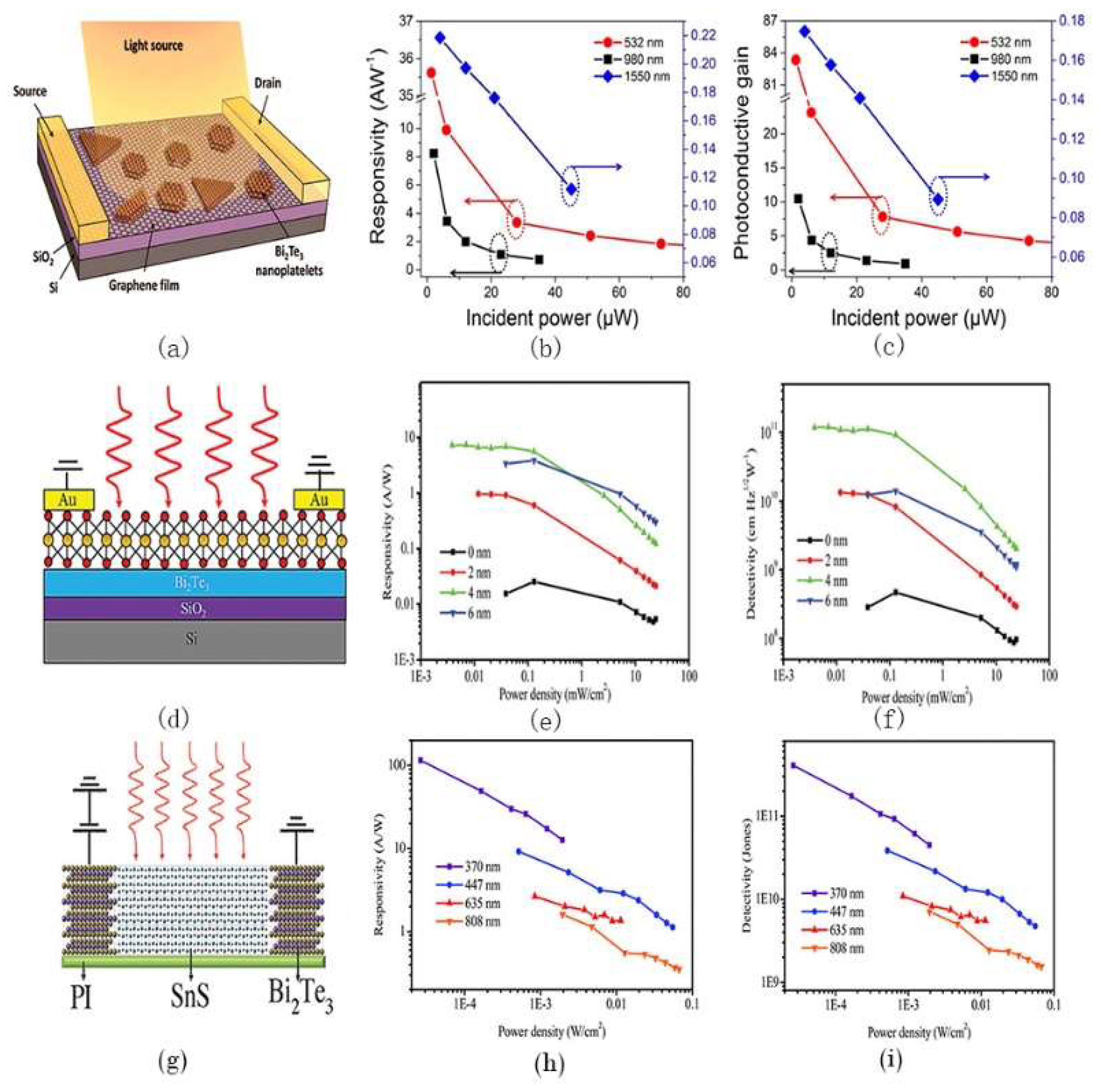
More recently, the combinations of layered materials to fabricate heterostructures have received tremendous attention due to their intrinsic quasi-2D nature and proper lattice mismatch, which can be very attractive in optoelectronic applications [60,61,62,63,64]. Typical layered semiconductors including graphene, transition metal dichalcogenides, and topological insulators are promising candidates and have been widely studied. In 2015, Qiao et al. reported a broadband photodetector based on graphene-Bi2Te3 heterostructure [65]. The Bi2Te3 nanocrystals were epitaxially grown on a graphene template using CVD technique. Since there is no dangling bond on either Bi2Te3 or graphene surface, such growth forms a novel van der Waals heterostructure with an atomic gapless interface. As shown in Figure 10a–c, due to the small lattice mismatch between Bi2Te3 and graphene, the photo-excited carriers can be effectively transferred and separated at the interface. High photoresponsivity of 35 A/W at 532 nm wavelength and an expanded detection spectral range have been successfully achieved. In 2016, Yao et al. published their work on the synthesis of Bi2Te3/WS2 heterostructure by using PLD deposition [66]. Although PLD is not favorable in preparing single-crystal films as mentioned above, the idea of integrating topological insulator and transition metal dichalcogenide to form 2D heterostructure is a significant advance in the next-generation photodetection. As demonstrated in Figure 10d–f, responsivity of 30.7 A/W with a pronounced detectivity of 2.3 × 1011 cm·Hz1/2·W−1, as well as a fast response within 20 ms have been obtained. Recently, a similar Bi2Te3/SnS 2D heterostructure photodetector has been reported by the same research team [67]. As shown in Figure 10g–i, it reached a high responsivity of 115 A/W, a large external quantum efficiency of 3.9 × 10⁴% and a superior detectivity of 4.1 × 1011 cm·Hz1/2·W−1, which are among the best figures-of-merit of 2D photodetectors so far. Such decent performance is originated from the effective carrier separation at the Bi2Te3/chalcogenide interface and carrier transport with high mobility at the topological insulator surface. With the wide spreading of the novel 2D transition metal dichalcogenide in various research fields, its combination with the vast infrastructure of topological insulator will definitely open the new pathways for advanced optoelectronic applications.
3.3. Magnetoelectric Device
Topological insulators have conductive surface states which are protected by time-reversal symmetry. Meanwhile, these states are related to the spin and the characteristic of QSH effect. Similar to the conventional QH effect, the topological structure in 3D topological insulators will lead to quantized electromagnetic response coefficients [68]. This means that when the time-reversal symmetry on the surface is broken, the quantized electromagnetic response will occur with such characteristics as induced magnetization by electric field or vice versa. This topologically new phenomenon is known as topological magnetoelectric effect (TME) [68,69].
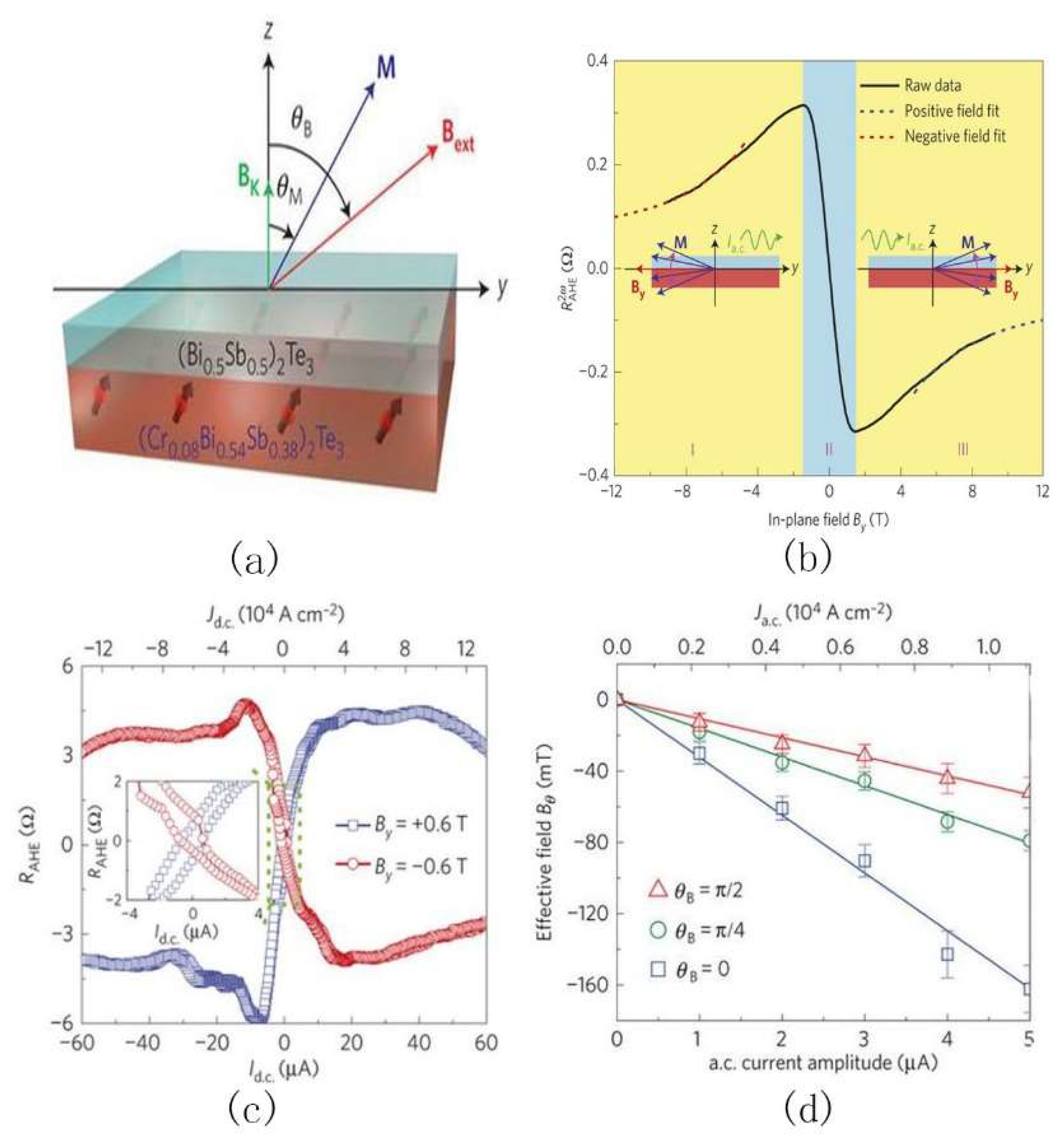
Theoretically, one of the easiest ways to generate a surface symmetry breaking field is by coating the topological insulator surface with magnetic impurities such as a layer of ferromagnetic material, and tuning the chemical potential near the Dirac point [69]. In this way, the heterojunction of topological insulator and ferromagnetic material can enable the demonstration or even controlling of the magnetization through external approaches. This could be very interesting in a lot of physical investigations such as the realization of magnetic monopole effect. Although the theoretical and simulation work of TME have been initiated since about 10 years ago [70,71,72], experimental work verifying or even using the theory for practical device application is still rarely seen. For example, Fujita et al. proposed a novel 3D topological insulator cell with ferromagnetic doping on the surface breaking the time-reversal symmetry [73]. Long-range magnetic order was thus induced and opened up an energy gap at the Dirac point. They claimed that this new type of device can be utilized in novel memory and magnetic sensor, since the readout process was protected by the quantized hall effect, so that the magnetic storage should be robust against perturbations such as edge roughness, impurities and defects. However, the experimental realization of this proposed memory cell is difficult in maintaining the proper Fermi level position and electrical programming/erasing or readout operations at the same time. This problem was partly solved by Fan et al. in 2014 [74]. In their work, they use MBE to epitaxially synthesize (Bi0.5Sb0.5)2Te3/(Cr0.08Bi0.54Sb0.38)2Te3 bilayer films. Conventionally, spin current generated in the heavy metal adjacent to a ferromagnet material is based on the spin-Hall effect, and can apply spin torques to the ferromagnetic layer resulting in current-induced magnetization manipulation [74]. Magnetically doped topological insulators (such as the Cr doping in this reference work) have been demonstrated to be good platform to study the spin-orbit torque due to the large spin-orbit coupling to invert the band structure. In the Cr-doped BiSbTe bilayer system (Figure 11a), spin accumulation will occur in the Cr-doped layer when passing a charge current due to the spin-Hall effect and the spin polarization. The accumulated angular momentum of spin can be transferred to the magnetization and affect the dynamics [74]. Figure 11b showing the second-harmonic anomalous hall effect resistance was used to calibrate the effective spin-orbit torque induced field. The magnetization switching can be realized through the charge current-induced spin-orbit torque, as shown in Figure 11c. The relationship between the effect spin-orbit field and the current amplitude was demonstrated in Figure 11d. This type of switching can be regarded as a direct utilization of the topological magnetoelectric effect involving the magnetization manipulation. Although the underlying mechanism of spin-orbit torque is still debated, the in-plane current-driven spin-orbit torque which stimulates the magnetization switching is a new mechanism towards memory and logic device applications [74].
Later in 2017, Wang et al. fabricated spin-orbit torque-driven magnetization switching in Bi2Se3/NiFe heterostructures at room temperature. The charge-to-spin conversion efficiency in Bi2Se3 films reached ~1–1.75 while the needed current density for the magnetization switching was just ~6 × 10⁵ A cm–2 which was orders of magnitude lower than the cases of heavy metals. This pave a new way for the topological insulator-based spintronic devices [75]. More recently, Bi0.9Sb0.1-based ultra-low power spin-orbit-torque switching was reported in 2018 [76]. The Bi0.9Sb0.1 thin films on Mn0.6Ga0.4 surface have high electrical conductivity (σ ~ 2.5 × 10⁵ Ω−1 m−1) and large spin Hall angle (θSH ~ 52) which can generate a spin-orbit field of 2770 Oe/(MA/cm2) while the critical switching current density was as low as 1.5 MA/cm2 in the bi-layers [76]. Although it was claimed that such BiSb system will be promising candidate for the industrial applications with topological insulators-based spin-orbit torque memory, the process integration of these novel materials still remains the challenging problem considering the realization of large spin Hall effect at room temperature and the controlling of surface orientation [76].
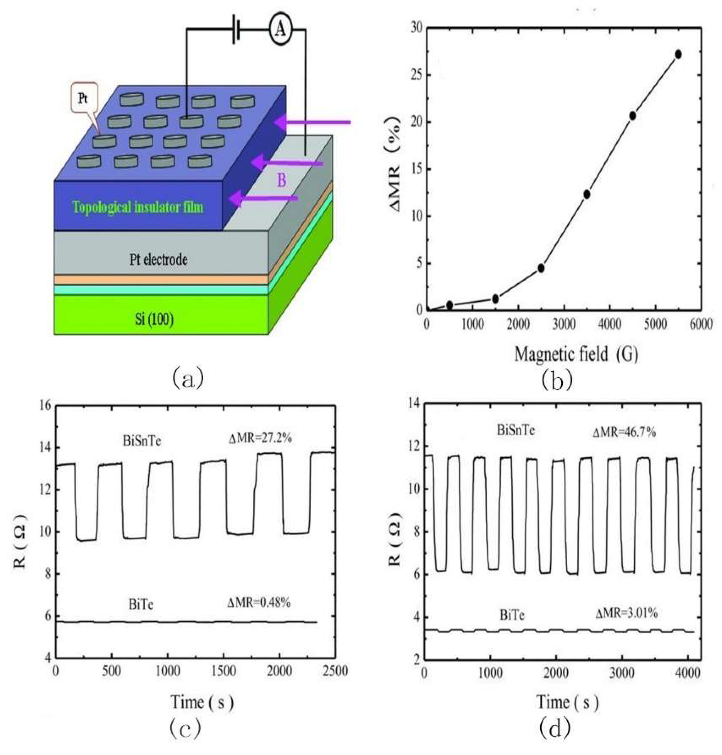
Compared to the above methods for magnetoelectric device applications, some other device design and mechanism have also been investigated. For example, Zhang et al. reported a novel magnetoresistance (MR) switching effect in 2012 by synthesizing Sn-doped Bi2Te3 thin films and integrated in a simple metal-insulator-metal device structure [77]. As shown in Figure 12, an external magnetic field was also applied to break the time-reversal symmetry. Different from the undoped Bi2Te3, in Sn-doped Bi2Te3, the bulk electrons will experience back scattering by Sn dopants, and the trajectory of the bulk electrons defined by the weak localization effect will be influenced by the time-reversal invariance, leading to a destroyed constructive interference of the electron’s wave function. This will further decrease the resistance exhibiting an MR switching effect [77]. No matter how the magnetoelectric effect or the magnetoresistance switching behavior was realized, there is still an obvious gap between the theoretical prediction and practical device verification and application towards novel spintronic and magnetoelectric device applications.
Considering back to the integration of topological insulator with ferromagnetic material, the spin injection and extraction through certain barriers are also interesting. This involves the spin-momentum locking of the 2D surface states in 3D topological insulators, which have great potential to realize dissipation-less transport and to achieve spin generators in spintronic devices. Existing theories and experiments have confirmed that the spin of electrons in the surface states of topological insulators is highly polarized, the energy band is reversed due to strong coupling of spin orbit and that the spin of electrons and the crystalline momentum are locked together called spin-momentum locking, forming a unique helical spin texture. Very recently, a 3D topological insulator spin valve has been reported with prominent switching behavior [78]. Bi2Te2Se nanoplatelets have been synthesized by using a catalyst-free vapor-solid method. A thin layer of insulating hexagonal boron nitride (hBN) was inserted separating the topological insulator and ferromagnetic electrode. By characterizing the contact resistance variation which is correlated with the spin valve switching, the functionality of the spin-polarized current carried by the helical surface states can be studied. The hysteresis in the switching curve reversed along with reversing the applied current when contact resistances were low while the polarity of the hysteresis was current-direction-independent under high contact resistances. This make it possible to modulate the spin exchange between the ferromagnetic material and topological insulator through the engineering of hBN layers [78].
The magnetoelectric device based on 3D topological insulator is an expanding subject with many theoretical and experimental issues remain uncertain. Further in-depth studies are needed to elucidate the mechanisms which can affect the topological magnetoelectric effect involving the detection, characterization and manipulation of magnetization, spin polarization, and spin filtering properties. Nevertheless, innovative spintronic devices utilizing various quantum effects can be expected in the future and it can be a big step in the advanced information technology.
3.4. Other Applications
Apart from the applications in field-effect transistor, optoelectronic device and magnetoelectric device described above, there are many other fields that topological insulator can be implemented in. For example, in 2008, Qi et al. employed the topological surface states to realize the detection of magnetic monopole [79]. In this theory, when an electric charge was approaching the surface of a topological insulator, a corresponding magnetic monopole charge can be induced acting as a mirror image. Hence, the detection of magnetic monopole can be interpreted by the measurement of the generated magnetic field. Besides, the conversion from a chiral Dirac fermion to a pair of neutral chiral Majorana fermions has also been realized, enabling the electrical detection of the interferometric signals [80]. Additionally, topological insulators can be used in batteries [81], gas sensors [82], solar cell [83] and memory devices [84] which have the superiority in quality factor and power consumption [73,84,85,86]. For example, Tian et al. observed the long-lived persistent electron spin polarization which was even unaffected with low temperature and removing current. This electrically controllable spin polarization makes it feasible to fabricate rechargeable spin battery and rewritable spin memory [81]. The sensing capabilities of topological insulators have been tested by Liu et al. by exposing the surface with conducting channels to various external environment [82]. A Bi2Se3-based organic polymer solar cell has been reported by Yuan et al. in 2015 with maximum photoelectric conversion efficiency of 4.37% [83], and a fast-speed non-volatile memory with write and read time as low as 20 nm has also been achieved based on 3D topological insulator materials [73]. Such applications with potential for significant innovations in future electronic devices are due to the attractive intrinsic properties of the topological insulators which are prominently distinguished from the conventional semiconductors. Nevertheless, great efforts are still needed for the synthetic topological insulator nanostructures to explore the strategies to realize new-concept and new-mechanism electronic devices.
4. Conclusions and Outlook
The scaling of Si-based CMOS technology has encountered greater challenges with more advanced technology node. On the other hand, topological insulators with the superiority of combing the spin and charge degrees of freedom has provided an alternative approach to overcome the physical limit. Low-power, high-performance spintronic devices can be achieved through the engineering over the spin-orbit coupling towards various applications such as nanoelectronics and optoelectronics [87]. Using different synthesis methods, novel topological insulator nanostructures can be effectively integrated in electronic devices leveraging the advantages afforded by the materials with current semiconductor technology. In this review, we briefly introduced synthetic approaches to grow topological insulator nanostructures and their device applications including field-effect transistor, optoelectronic device, magnetoelectric device and so forth. Through the development of 2D HgTe/CdTe quantum well to 3D topological insulators, the application of this series of materials have been extended to more theoretical and experimental research fields. The excellent device performance is originated from the unique properties of the surface states, and the enhanced topological feature in synthetic high-quality nanostructures with greater surface-to-volume ratio. So far, topological insulator nanowires, nanoribbons and nanoplates have attracted more interests because they will not only enable high-quality single crystal nanostructures but also facilitate advanced device architecture allowing for various characterization and manipulation methods with external means.
Topological insulators can have an enlarged scenario for future practical application, specifically in the interdisciplinary fields including condensed matter physics, microelectronics, information technology and so on. The intriguing metallic surface states make them promising candidate in new-concept spintronic devices, and the natural property that the surface has one Dirac point without spin degeneracy can give rise to the possibility in generating particles that can be utilized in quantum computing. Moreover, Majorana fermions which can be created in the interface between a topological insulator and a superconductor are just one step towards an error-prohibit topological quantum computer [88]. Actually, the current major bottleneck for topological insulators to be integrated in spintronic devices and quantum computing systems lies in the controllability over the combination with magnetic material. Recently, hybrid synthetic Bi2Se3 and EuS system has been reported in which EuS could maintain its stable magnetic properties up to room temperature, and the proximity-induced magnetism at the Bi2Se3/EuS interface can pave the way for energy-efficient topological control mechanism for future spin-based technologies [89]. So far, although the realization of surface state manipulation and heterogeneous integration can only be achieved preliminarily, further engineering on the synthetic process and device optimization can still be expected to open up a suite of potential application in novel nanoelectronics, optoelectronics, and spintronics.
Funding
This research was funded by the NSFC (61704030, 61376092 and 61427901), the Shanghai Pujiang Program (17PJ1400500), 02 State Key Project (2017ZX02315005), and Program of Shanghai Subject Chief Scientist (14XD1400900).
Conflicts of Interest
The authors declare no conflict of interest.
References
- Klitzing, K.V.; Dorda, G.; Pepper, M. New Method for High-Accuracy Determination of the Fine-Structure Constant Based on Quantized Hall Resistance. Phys. Rev. Lett. 1980, 45, 494–497. [Google Scholar] [CrossRef]
- Qi, X.L.; Zhang, S.C. The quantum spin Hall effect and topological insulators. Phys. Today 2010, 63, 33–38. [Google Scholar] [CrossRef] [Green Version]
- Wang, G. The Symmetry Broken State of the 2D and 3D Topological Insulator. M.E. Thesis, Southeast University, Nanjing, China, 2013. [Google Scholar]
- Hasan, M.Z.; Kane, C.L. Colloquium: Topological insulators. Rev. Mod. Phys. 2010, 82, 3045–3067. [Google Scholar] [CrossRef]
- Bernevig, B.A.; Hughes, T.L.; Zhang, S.C. Quantum Spin Hall Effect and Topological Phase Transition in HgTe Quantum Wells. Science 2006, 314, 1757–1761. [Google Scholar] [CrossRef] [PubMed] [Green Version]
- König, M.; Wiedmann, S.; Brüne, C.; Roth, A.; Buhmann, H.; Molenkamp, L.W.; Qi, X.L.; Zhang, S.C. Quantum spin hall insulator state in HgTe quantum wells. Science 2007, 318, 766–770. [Google Scholar]
- Liang, F.; Kane, C.L. Topological Insulators with Inversion Symmetry. Phys. Rev. 2007, 76, 045302. [Google Scholar]
- Hong, S.S.; Kundhikanjana, W.; Cha, J.J.; Lai, K.; Kong, D.; Meister, S.; Kelly, M.A.; Shen, Z.X.; Cui, Y. Ultrathin topological insulator Bi2Se3 nanoribbons exfoliated by atomic force microscopy. Nano Lett. 2010, 10, 3118–3122. [Google Scholar] [CrossRef] [PubMed]
- Qu, D.X.; Hor, Y.S.; Xiong, J.; Cava, R.J.; Ong, N.P. Quantum oscillations and hall anomaly of surface states in the topological insulator Bi2Te3. Science 2010, 329, 821–824. [Google Scholar] [CrossRef] [PubMed]
- Cho, S.; Butch, N.P.; Paglione, J.; Fuhrer, M.S. Insulating behavior in ultrathin bismuth selenide field effect transistors. Nano Lett. 2012, 11, 1925–1927. [Google Scholar] [CrossRef] [PubMed]
- Mciver, J.W.; Hsieh, D.; Steinberg, H.; Jarillo-Herrero, P.; Gedik, N. Control over topological insulator photocurrents with light polarization. Nat. Nanotechnol. 2012, 7, 96–100. [Google Scholar] [CrossRef] [PubMed] [Green Version]
- Li, Y.Y.; Wang, G.; Zhu, X.G.; Liu, M.H.; Ye, C.; Chen, X.; Wang, Y.Y.; He, K.; Wang, L.L.; Ma, X.C.; et al. Intrinsic Topological Insulator Bi2Te3 Thin Films on Si and Their Thickness Limit. Adv. Mater. 2010, 22, 4002–4007. [Google Scholar] [CrossRef] [PubMed]
- Zhang, T.; Cheng, P.; Chen, X.; Jia, J.F.; Ma, X.; He, K.; Wang, L.; Zhang, H.; Dai, X.; Fang, Z.; et al. Experimental Demonstration of Topological Surface States Protected by Time-Reversal Symmetry. Phys. Rev. Lett. 2009, 103, 266803. [Google Scholar] [CrossRef] [PubMed] [Green Version]
- Liu, X.; Smith, D.J.; Cao, H.; Chen, Y.; Fan, J.; Zhang, Y.; Pimpinella, R.E.; Dobrowolska, M.; Furdyna, J.K. Characterizations of Bi2Te3 and Bi2Se3 topological insulators grown by MBE on (100) GaAs substrates. J. Vac. Sci. Technol. B 2012, 30, 02B103. [Google Scholar] [CrossRef]
- Wang, Q.; Cai, K.; Li, J.; Huang, Y.; Wang, Z.; Xu, K.; Wang, F.; Zhan, X.; Wang, F.; Wang, K.; et al. Rational Design of Ultralarge Pb1-x Snx Te Nanoplates for Exploring Crystalline Symmetry-Protected Topological Transport. Adv. Mater. 2016, 28, 617–623. [Google Scholar] [CrossRef] [PubMed]
- Bendt, G.; Zastrow, S.; Nielsch, K.; Mandal, P.S.; Barriga, J.S.C.; Raderc, O.; Schulz, S. Stephan Deposition of topological insulator Sb2Te3 films by an MOCVD process. J. Mater. Chem. A 2014, 2, 8215–8222. [Google Scholar] [CrossRef]
- Waner, R.S.; Ellis, W.C. Vaporliquid-solid mechanism of single crystal growth. Appl. Phys. Lett. 1964, 4, 89–90. [Google Scholar] [CrossRef]
- Zhu, H.; Li, Q.; Yuan, H.; Baumgart, H.; Ioannou, D.E.; Richter, C.A. Self-aligned multi-channel silicon nanowire field-effect transistors. Solid State Electron. 2012, 78, 92–96. [Google Scholar] [CrossRef]
- Peng, H.; Lai, K.; Kong, D.; Meister, S.; Chen, Y.; Qi, X.; Zhang, S.; Shen, Z.; Cui, Y. Aharonov-Bohm interference in topological insulator nanoribbons. Nat. Mater. 2009, 9, 225. [Google Scholar] [CrossRef] [PubMed]
- Liu, C.; Zhang, H.; Sun, Z.; Ding, K.; Mao, J.; Shao, Z.; Jie, J. Topological Insulator Bi2Se3 Nanowire/Si Heterostructure Photodetector with Ultrahigh Responsivity and Broadband Response. J. Mater. Chem. C 2016, 4, 5648–5655. [Google Scholar] [CrossRef]
- Xiu, F.; He, L.; Wang, Y.; Cheng, L.; Chang, L.; Lang, M.; Huang, G.; Kou, X.; Zhou, Y.; Jiang, X.; et al. Manipulating surface states in topological insulator nanoribbons. Nat. Nanotechnol. 2011, 6, 216–221. [Google Scholar] [CrossRef] [PubMed]
- Schlenk, T.; Bianchi, M.; Koleini, M.; Eich, A.; Pietzsch, O.; Wehling, T.O.; Frauenheim, T.; Balatsky, A.; Mi, J.L.; Iversen, B.B.; et al. Controllable magnetic doping of the surface state of a topological insulator. Phys. Rev. Lett. 2013, 110, 1–10. [Google Scholar] [CrossRef] [PubMed]
- Steinberg, H.; Gardner, D.R.; Lee, Y.S.; Jarillo-Herrero, P. Surface state transport and ambipolar electric field effect in Bi2Se3 nanodevices. Nano. Lett. 2010, 10, 5032. [Google Scholar] [CrossRef] [PubMed] [Green Version]
- Chen, Y.P. Graphene and topological insulator based transistors: Beyond computing applications. In Proceedings of the Device Research Conference, University Park, TX, USA, 18–20 June 2012; pp. 37–38. [Google Scholar]
- Yang, F.; Taskin, A.A.; Sasaki, S.; Segawa, K.; Ohno, Y.; Matsumoto, K.; Ando, Y. Dual-Gated Topological Insulator Thin-Film Device for Efficient Fermi-Level Tuning. ACS Nano 2015, 9, 4050–4055. [Google Scholar] [CrossRef] [PubMed]
- Son, J.; Banerjee, K.; Brahlek, M.; Koirala, N.; Lee, S.; Ahn, J.; Oh, S.; Yang, H. Conductance modulation in topological insulator Bi2Se3 thin films with ionic liquid gating. Appl. Phys. Lett. 2013, 103, 016801. [Google Scholar] [CrossRef]
- Zhang, Z.; Feng, X.; Guo, M.; Li, K.; Zhang, J.; Ou, Y.; Feng, Y.; Wang, L.; Chen, X.; He, K.; et al. Electrically tuned magnetic order and magnetoresistance in a topological insulator. Nat. Commun. 2014, 5, 4915. [Google Scholar] [CrossRef] [PubMed] [Green Version]
- Zhu, H.; Zhao, E.; Richter, C.A.; Li, Q. Topological Insulator Bi2Se3 Nanowire Field Effect Transistors. Ecs Trans. 2014, 64, 51–59. [Google Scholar] [CrossRef]
- Chang, J.; Register, L.F.; Banerjee, S.K. Topological insulator Bi2Se3 thin films as an alternative channel material in metal-oxide-semiconductor field-effect transistors. J. Appl. Phys. 2012, 112, 3045–3067. [Google Scholar] [CrossRef]
- Liu, Y.H.; Chong, C.W.; Fanchiang, C.M.; Huang, J.C.A.; Han, H.C.; Li, Z.J.; Qiu, H.L.; Li, Y.C.; Liu, C.P. Ultrathin (Bi1-xSbx)2Se3 field effect transistor with large ON/OFF ratio. Acs Appl. Mater. Interfaces 2017, 9, 12859–12864. [Google Scholar] [CrossRef] [PubMed]
- Xu, S.Y.; Neupane, M.; Liu, C.; Zhang, D.; Richardella, A.; AndrewWray, L.; Alidoust, N.; Leandersson, M.; Balasubramanian, T.; Sánchez-Barriga, J.; et al. Hedgehog Spin Texture and Berry’s Phase Tuning in a Magnetic Topological Insulator. Nat. Phys. 2012, 8, 616–622. [Google Scholar] [CrossRef]
- Kou, M.X.; Lang, Y.; Fan, Y.; Jiang, T.; Nie, J.; Zhang, W.; Jiang, Y.; Wang, Y.; Yao, L.H. Interplay between Different Magnetisms in Cr-Doped Topological Insulators. ACS Nano 2013, 10, 9205–9212. [Google Scholar] [CrossRef] [PubMed]
- Zhu, H.; Richter, C.A.; Zhao, E.; Bonevich, J.E.; Kimes, W.A.; Jang, H.J.; Yuan, H.; Li, H.; Arab, A.; Kirillov, O.; et al. Topological insulator Bi2Se3 nanowire high performance field-effect transistors. Sci. Rep. 2013, 3, 1757. [Google Scholar] [CrossRef]
- Liu, H.; Ye, P.D. Atomic-layer-deposited Al2O3 on Bi2Te3 for topological insulator field-effect transistors. Appl. Phys. Lett. 2011, 99, 3045. [Google Scholar] [CrossRef]
- Wray, L.A.; Xu, S.; Neupane, M.; Xia, Y.; Hsieh, D.; Qian, D.; Fedorov, A.V.; Lin, H.; Basak, S.; Hor, Y.S.; et al. Electron dynamics in topological insulator based semiconductor-metal interfaces (topological p-n interface based on Bi2Se3 class). arXiv, 2011; arXiv:1105.4794. [Google Scholar]
- Koirala, N.; Brahlek, M.; Salehi, M.; Wu, L.; Dai, J.; Waugh, J.; Nummy, T.; Han, M.G.; Moon, J.; Zhu, Y.; et al. Record surface state mobility and quantum Hall effect in topological insulator thin films via interface engineering. Nano Lett. 2015, 8, 3045. [Google Scholar] [CrossRef] [PubMed]
- Hao, G.; Qi, X.; Xue, L.; Cai, C.; Li, J.; Wei, X.; Zhong, J. Fermi level tuning of topological insulator Bi2(SexTe1−x)3 nanoplates. J. Appl. Phys. 2013, 113, 024306. [Google Scholar] [CrossRef]
- Sacépé, B.; Oostinga, J.B.; Li, J.; Ubaldini, A.; Couto, N.J.; Giannini, E.; Morpurgo, A.F. Gate-tuned normal and superconducting transport at the surface of a topological insulator. Nat. Commun. 2011, 2, 575. [Google Scholar] [CrossRef] [PubMed] [Green Version]
- Zhang, T.; Levy, N.; Ha, J.; Kuk, Y.; Stroscio, J.A. Scanning Tunneling Microscopy of Gate Tunable Topological Insulator Bi2Se3 Thin Films. Phys. Rev. B 2013, 87, 1504–1509. [Google Scholar]
- Brinkman, A.; Snelder, M.; Brocks, G.H.L.A. Towards Controlling the Fermi Energy in Topological Materials. Master’s Thesis, University of Twente, Enschede, The Netherlands, 2014. [Google Scholar]
- Taskin, A.A.; Legg, H.F.; Yang, F.; Sasaki, S.; Kanai, Y.; Matsumoto, K.; Rosch, A.; Ando, Y. Planar Hall effect from the surface of topological insulators. Nat. Commun. 2017, 8, 1340. [Google Scholar] [Green Version]
- Walsh, L.A.; Green, A.J.; Addou, R.; Nolting, W.; Cormier, C.R.; Barton, A.T.; Mowll, T.R.; Yue, R.; Lu, N.; Kim, J.; et al. Fermi Level Manipulation through Native Doping in the Topological Insulator Bi2Se3. ACS Nano 2018, 12, 6310–6318. [Google Scholar] [CrossRef] [PubMed]
- Hong, S.S.; Cha, J.J.; Kong, D.; Cui, Y. Ultra-low carrier concentration and surface-dominant transport in antimony-doped Bi2Se3 topological insulator nanoribbons. Nat. Commun. 2012, 3, 757. [Google Scholar] [CrossRef] [PubMed] [Green Version]
- Hor, Y.S.; Richardella, A.; Roushan, P.; Xia, Y.; Checkelsky, J.G.; Yazdani, A.; Hasan, M.Z.; Ong, N.P.; Cava, R.J. p-type Bi2Se3 for topological insulator and low temperature thermoelectric applications. Phys. Rev. B 2009, 79, 195208. [Google Scholar] [CrossRef]
- Wang, Y.; Xiu, F.; Cheng, L.; He, L.; Lang, M.; Tang, J.; Kou, X.; Yu, X.; Jiang, X.; Chen, Z.; et al. Gate-Controlled Surface Conduction in Na-Doped Bi2Te3 Topological Insulator Nanoplates. Nano Lett. 2012, 12, 1170–1175. [Google Scholar] [CrossRef] [PubMed]
- Inoue, J.; Tanaka, A. Photoinduced transition between conventional and topological insulators in two-dimensional electronic systems. Phys. Rev. Lett. 2010, 105, 017401. [Google Scholar] [CrossRef] [PubMed]
- Hosur, P. Circular photogalvanic effect on topological insulator surfaces: Berry-curvature-dependent response. Phys. Rev. B 2011, 83, 426–432. [Google Scholar] [CrossRef]
- Zheng, K.; Luo, L.B.; Zhang, T.F.; Liu, Y.H.; Yu, Y.Q.; Lu, R.; Qiu, H.L.; Li, Z.J.; Huang, J.C.A. Optoelectronic characteristics of a near infrared light photodetector based on a topological insulator Sb2Te3 film. J. Mater. Chem. C 2015, 3, 9154–9160. [Google Scholar] [CrossRef]
- Zhang, H.; Liu, C.-X.; Qi, X.-L.; Dai, X.; Fang, Z.; Zhang, S.-C. Topological insulators in Bi2Se3, Bi2Te3 and Sb2Te3 with a single Dirac cone on the surface. Nat. Phys. 2009, 5, 438–442. [Google Scholar] [CrossRef] [Green Version]
- Sharma, A.; Srivastava, A.K.; Senguttuvan, T.D.; Husale, S. Robust broad spectral photodetection (UV-NIR) and ultra high responsivity investigated in nanosheets and nanowires of Bi2Te3under harsh nano-milling conditions. Sci. Rep. 2017, 7, 17911. [Google Scholar] [CrossRef] [PubMed]
- Fei, F.; Wei, Z.; Wang, Q.J.; Lu, P.; Wang, S.; Qin, Y.; Pan, D.; Zhao, B.; Wang, X.; Sun, J.; et al. Solvothermal synthesis of lateral heterojunction Sb2Te3/Bi2Te3 nanoplates. Nano Lett. 2015, 15, 5905–5911. [Google Scholar] [CrossRef] [PubMed]
- Chong, S.K.; Han, K.B.; Nagaoka, A.; Tsuchikawa, R.; Liu, R.; Liu, H.; Vardeny, Z.V.; Pesin, D.A.; Lee, C.; Sparks, T.D.; et al. Topological Insulator-Based van der Waals Heterostructures for Effective Control of Massless and Massive Dirac Fermions. arXiv, 2018; arXiv:1805.09478. [Google Scholar]
- Wang, X.B.; Cheng, L.; Wu, Y.; Zhu, D.P.; Wang, L.; Zhu, J.; Yang, H.; Chia, E.E.M. Topological-insulator-based terahertz modulator. Sci. Rep. 2017, 7, 13486. [Google Scholar] [CrossRef] [PubMed] [Green Version]
- Yoshimi, R.; Tsukazaki, A.; Kikutake, K.; Checkelsky, J.G.; Takahashi, K.S.; Kawasaki, M.; Tokura, Y. Dirac electron states formed at the, heterointerface between a topological, insulator and a conventional semiconductor. Nat. Mater. 2014, 13, 253. [Google Scholar] [CrossRef] [PubMed]
- Pang, M.Y.; Li, W.S.; Wong, K.H.; Surya, C. Electrical and optical properties of bismuth telluride/gallium nitride heterojunction diodes. J. Non-Cryst. Solids 2008, 354, 4238–4241. [Google Scholar] [CrossRef]
- Yao, J.; Shao, J.; Wang, Y.; Zhao, Z.; Yang, G. Ultra-broadband and high response of the Bi2Te3-Si heterojunction and its application as a photodetector at room temperature in harsh working environments. Nanoscale 2015, 7, 12535–12541. [Google Scholar] [CrossRef] [PubMed]
- Zhang, H.; Zhang, X.; Liu, C.; Lee, S.T.; Jie, J. High-Responsivity, High-Detectivity, Ultrafast Topological Insulator Bi2Se3/Silicon Heterostructure Broadband Photodetectors. ACS Nano 2016, 10, 5113. [Google Scholar] [CrossRef] [PubMed]
- Zhang, H.; Man, B.; Zhang, Q. Topological Crystalline Insulator SnTe/Si Vertical Heterostructure Photodetectors for High-performance Near-infrared Detection. Acs Appl. Mater. Interfaces 2017, 9, 14067–14077. [Google Scholar] [CrossRef] [PubMed]
- Gu, S.; Ding, K.; Pan, J.; Shao, Z.; Mao, J.; Zhang, X.; Jie, J. Self-driven, broadband and ultrafast photovoltaic detectors based on topological crystalline insulator SnTe/Si heterostructures. J. Mater. Chem. A 2017, 5, 11171–11178. [Google Scholar] [CrossRef]
- An, X.; Liu, F.; Jung, Y.J.; Kar, S. Tunable grapheme-silicon heterojunctions for ultrasensitive photodetection. Nano Lett. 2017, 13, 909–916. [Google Scholar] [CrossRef] [PubMed]
- Zhang, K.; Fang, X.; Wang, Y.; Wan, Y.; Song, Q.; Zhai, W.; Li, Y.; Ran, G.; Ye, Y.; Dai, L. Ultrasensitive near-infrared photodetectors based on graphene-MoTe2-graphene vertical van der Waals heterostructure. ACS Appl. Mater. Interfaces 2017, 9, 5392–5398. [Google Scholar] [CrossRef] [PubMed]
- Liang, F.X.; Gao, Y.; Xie, C.; Tong, X.W.; Li, Z.J.; Luo, L.B. Recent advances in the fabrication of graphene–ZnO heterojunctions for optoelectronic device applications. J. Mater. Chem. C 2018, 6, 3815–3833. [Google Scholar] [CrossRef]
- Huo, N.; Yang, Y.; Li, J. Optoelectronics based on 2D TMDs and heterostructures. J. Semicond. 2017, 38, 2–10. [Google Scholar] [CrossRef]
- Sun, M.; Xie, D.; Sun, Y.; Li, W.; Teng, C.; Xu, J. Lateral multilayer/monolayer MoS2 heterojunction for high performance photodetector applications. Sci. Rep. 2017, 7, 4505. [Google Scholar] [CrossRef] [PubMed] [Green Version]
- Qiao, H.; Yuan, J.; Xu, Z.; Chen, C.; Lin, S.; Wang, Y.; Song, J.; Liu, Y.; Khan, O.; Hoh, H.Y.; et al. Broadband photodetectors based on graphene-Bi2Te3 heterostructure. ACS Nano 2015, 9, 1886–1894. [Google Scholar] [CrossRef] [PubMed]
- Yao, J.; Zheng, Z.; Yang, G. Layered-material WS2/topological insulator Bi2Te3 heterostructure photodetector with ultrahigh responsivity in the range from 370 to 1550 nm. J. Mater. Chem. C 2016, 4, 7831–7840. [Google Scholar] [CrossRef]
- Yao, J.; Yang, G. Flexible and High-Performance All-2D Photodetector for Wearable Devices. Small 2018, 14, 1704524. [Google Scholar] [CrossRef] [PubMed]
- Qi, X.L.; Zhang, S.C. Topological insulators and superconductors. Rev. Mod. Phys. 2011, 83, 1057–1110. [Google Scholar] [CrossRef] [Green Version]
- Qi, X.L. Topological field theory of time-reversal invariant insulators. Phys. Rev. B. 2008, 78, 2599–2604. [Google Scholar] [CrossRef]
- Crosse, J.A. Theory of topological insulator waveguides: Polarization control and the enhancement of the magneto-electric effect. Sci. Rep. 2017, 7, 43115. [Google Scholar] [CrossRef] [PubMed]
- Nomura, K.; Nagaosa, N. Surface-quantized anomalous Hall current and the magnetoelectric effect in magnetically disordered topological insulators. Phys. Rev. Lett. 2011, 106, 166802. [Google Scholar] [CrossRef] [PubMed]
- Grushin, A.G.; Neupert, T.; Chamon, C.; Mudry, C. Enhancing the stability of a fractional Chern insulator against competing phases. Phys. Rev. B 2012, 86, 205125. [Google Scholar] [CrossRef]
- Fujita, T.; Jalil, M.B.A.; Tan, S.G. Topological Insulator Cell for Memory and Magnetic Sensor Applications. Appl. Phys. Exp. 2011, 4, 544–548. [Google Scholar] [CrossRef]
- Fan, Y.; Upadhyaya, P.; Kou, X.; Lang, M.; Takei, S.; Wang, Z.; Tang, J.; He, L.; Chang, L.T.; Montazeri, M.; et al. Magnetization switching through giant spin-orbit torque in a magnetically doped topological insulator heterostructure. Nat. Mater. 2014, 13, 699–704. [Google Scholar] [CrossRef] [PubMed]
- Wang, Y.; Zhu, D.; Wu, Y.; Yang, Y.; Yu, J.; Ramaswamy, R.; Mishra, R.; Shi, S.; Elyasi, M.; Teo, K.L.; Wu, Y.; Yang, H.; et al. Room temperature magnetization switching in topological insulator-ferromagnet heterostructures by spin-orbit torques. Nat. Commun. 2017, 8, 1364. [Google Scholar] [CrossRef] [PubMed] [Green Version]
- Khang, N.H.D.; Ueda, Y.; Hai, P.N. A conductive topological insulator with large spin Hall effect for ultralow power spin–orbit torque switching. Nat. Mater. 2018, 17, 808–813. [Google Scholar] [CrossRef] [PubMed]
- Zhang, H.B.; Yu, H.L.; Bao, D.H.; Li, S.W.; Wang, C.X.; Yang, G.W. Magnetoresistance Switch Effect of a Sn-Doped Bi2Te3 Topological Insulator. Adv. Mater. 2012, 24, 132. [Google Scholar] [CrossRef] [PubMed]
- Vaklinova, K.; Polyudov, K.; Burghard, M.; Kern, K. Spin filter effect of hBN/Co detector electrodes in a 3D topological insulator spin valve. J. Phys. 2018, 30, 105302. [Google Scholar] [CrossRef] [PubMed] [Green Version]
- Qi, X.L.; Li, R.D.; Zang, J.D.; Zhang, S.C. Inducing a magnetic monopole with topological surface states. Science 2009, 323, 1184–1187. [Google Scholar] [CrossRef] [PubMed]
- Akhmerov, A.R.; Nilsson, J.; Beenakker, C.W.J. Electrically detected interferometry of Majorana fermions in a topological insulator. Phys. Rev. Lett. 2009, 102, 216404. [Google Scholar] [CrossRef] [PubMed]
- Tian, J.; Hong, S.; Miotkowski, I.; Datta, S.; Chen, Y.P. Observation of current-induced, long-lived persistent spin polarization in a topological insulator: A rechargeable spin battery. Sci. Adv. 2017, 3, e1602531. [Google Scholar] [CrossRef] [PubMed]
- Liu, B.; Xie, W.; Li, H.; Wang, Y.; Cai, D.; Wang, D.; Wang, L.; Liu, Y.; Li, Q.; Wang, T. Surrounding sensitive electronic properties of Bi2Te3 nanoplates-potential sensing applications of topological insulators. Sci. Rep. 2014, 4, 4639. [Google Scholar] [CrossRef] [PubMed]
- Yuan, Z. The Application of Novel Interfacial Materials and Structure in Organic-Inorganic Solar Cells. Master's Thesis, Soochow University, Soochow, China, 2015. [Google Scholar]
- Wang, Y.; Yu, H. Design exploration of ultra-low power non-volatile memory based on topological insulator. In Proceedings of the IEEE/ACM International Symposium on Nanoscale Architectures (NANOARCH), Amsterdam, The Netherlands, 4–6 July 2012; Volume 8474, pp. 30–35. [Google Scholar]
- Paudel, H.P.; Leuenberger, M.N. A 3D topological insulator quantum dot for optically controlled quantum memory and quantum computing. In Proceedings of the APS March Meeting, American Physical Society, Baltimore, MD, USA, 18–22 March 2013; pp. 4049–4056. [Google Scholar]
- Reza, A.K.; Fong, X.; Azim, Z.A.; Roy, K. Modeling and Evaluation of Topological Insulator/Ferromagnet Heterostructure-Based Memory. IEEE Trans. Electron. Dev. 2016, 63, 1359–1367. [Google Scholar] [CrossRef]
- Wang, K.L.; Kou, X.; Upadhyaya, P.; Fan, Y.; Shao, Q.; Yu, G.; Amiri, P.K. Electric-Field Control of Spin-Orbit Interaction for Low-Power Spintronics. Proc. IEEE 2016, 104, 1974–2008. [Google Scholar] [CrossRef]
- Moore, J.E. The birth of topological insulators. Nature 2010, 464, 194–198. [Google Scholar] [CrossRef] [PubMed]
- Katmis, F.; Lauter, V.; Nogueira, F.S.; Assaf, B.A.; Jamer, M.E.; Wei, P.; Satpati, B.; Freeland, J.W.; Eremin, I.; Heiman, D. A high-temperature ferromagnetic topological insulating phase by proximity coupling. Nature 2016, 533, 513–516. [Google Scholar] [CrossRef] [PubMed]
Figure 1.
Raman mapping patterns (the position differences of the E2g peak) of (a) Bi2Te3 and (b) Bi2Se3 with the thickness of 136 nm and 150 nm, respectively. The area of measurement is 15 μm × 15 μm. High-resolution transmission electron microscopy (HRTEM) images of (c) Bi2Te3 and (d) Bi2Se3 topological insulators grown on a GaAs substrate [14]. Reproduced with permission from [14], Copyright AIP Publishing, 2012.

Figure 2.
(a) SEM image of the vertically oriented Pb1−xSnxTe nanoplates. Inset: crystal structure model of Pb1−xSnxTe. (b) 15°-tilted SEM images of the vertically oriented Pb1−xSnxTe nanoplates. (c) SEM and (d) AFM images of the planar Pb1−xSnxTe nanoplate [15]. Reproduced with permission from [15], Copyright John Wiley and Sons, 2015.

Figure 3.
(a,b) SEM images of the as-grown Bi2Se3 nanoribbons by using VLS method [19]. (c) TEM image of a Bi2Se3 nanoribbon with Au nanoparticle at the tip. (d) HRTEM image of the edge of the Bi2Se3 nanoribbon with smooth surface. Inset: the selected-area electron diffraction (SAED) pattern shows the single-crystal characteristic of Bi2Se3 nanoribbon [19]. SEM images of the Bi2Se3 nanowires with (e) low magnification and (f) high magnification [20]. (g) Low-resolution TEM image of a single Bi2Se3 nanowire. (h) HRTEM image of the Bi2Se3 nanowire [20]. Reproduced with permission from [19], Copyright Springer Nature, 2009. Reproduced with permission from [20], Copyright Royal Society of Chemistry, 2016.

Figure 4.
(a) TEM image of the cross-section of a Bi2Se3 nanowire field-effect transistor (FET); (b) IDS-VGS of Bi2Se3 nanowire FET at 77 K; (c) Linear-scale IDS-VDS curves for VGS from −4.4 V to −1.4 V at 77 K. (d) The illustration of IDS-VGS at temperature from 77 K to 295 K with VDS = 50 mV. Inset: the relationship between ln(IDS) at Off state and 1/kT [28]. Reproduced with permission from [28], Copyright Electrochemical Society, 2014.

Figure 5.
(a) The schematic of ultrathin (Bi1−xSbx)2Se3 field effect transistor on SrTiO3 substrate. (b) Rs vs. Vg of the FET based on 5 nm (Bi1−xSbx)2Se3 film. (c) Mechanism of the large On/Off ratio: the Fermi level in the ultra-thin topological insulator film can be tuned within or close to the surface gap in both bottom and top surface states [31]. Reproduced with permission from [31], Copyright American Chemical Society, 2017.

Figure 6.
(a) A schematic of back-gate FET based on 40-nm-thick Bi2Te3 nanoplate with ~1.2 μm channel length. (b) Hall measurement results showing the type transition from n-type to p-type by changing gate voltage at 1.9 K. (c) SdH oscillations indexed by different Landau levels under increasing gate voltage at 1.9 K. (d) Landau level as a function of 1/B under different voltages [43]. Reproduced with permission from [43], Copyright Springer Nature, 2012.

Figure 7.
(a) The schematic illustration of Sb2Te3-based near infrared (NIR) light photodetector. (b) The X-ray diffraction image of Sb2Te3 film grown by MBE. (c,d) are the I–V characteristics of Sb2Te3 film in dark and under illumination, respectively, at the temperature range of 8.5–300 K. (e) Photoresponse of the Sb2Te3-based photodetector at 45 K under voltages of 0.01 V, 0.1 V and 1 V. (f) One cycle of the photoresponse at a temperature of 45 K and 0.1 V voltage [48]. Reproduced with permission from [48], Copyright Royal Society of Chemistry, 2015.

Figure 8.
(a) Schematic structure of the Bi2Te3/Si-based photodetector. The time-dependent switching behavior under illumination of (b) 370 nm and (c) 118.8 μm at room temperature [56]. (d) The schematic illustration of the Bi2Se3/Si heterostructure device with Au and In−Ga electrodes [57]. (e) Photoresponsivity of the Bi2Se3/Si heterostructure photodetector as a function of light intensity at −1 V and 0 V at room temperature. (f) Transient response of the photodetector to the high-frequency (60 KHz) light signal at room temperature [57]. (g) The schematic illustration of Bi2Se3 nanowire/Si heterostructure photodetector [21]. (h) The responsivity and detectivity of Bi2Se3 nanowire/Si heterostructure photodetector versus light intensity at room temperature. (i) The response time (rise and decay times) investigation of the photodetector with magnified current response at room temperature [21]. Reproduced with permission from [21], Copyright Royal Society of Chemistry, 2016. Reproduced with permission from [56], Copyright RSC, 2015. Reproduced with permission from [57], Copyright American Chemical Society, 2016.

Figure 9.
(a) The cross-sectional schematic diagram of SnTe/Si vertical heterostructure photodetector with Au top electrode and In-Ga bottom electrode. (b) The photoresponsivity and detectivity vs. light intensity curves under 1064 nm light illumination at zero bias voltage. (c) The relative balance (Vmax − Vmin)/Vmax ×100% of the photovoltage of the device as a function of frequency. Inset: schematic diagram of measurement setup [58]. (d) Schematic illustration of the SnTe/Si heterostructure photovoltaic detectors. (e) The magnified photoresponse demonstrating the rise time of 8 μs. (f) The responsivity and detectivity as a function of light intensity at zero bias voltage and room temperature [59]. Reproduced with permission from [58], Copyright American Chemical Society, 2017. Reproduced with permission from [59], Copyright Royal Society of Chemistry, 2017.

Figure 10.
(a) The schematic structure of the graphene-Bi2Te3 heterostructure phototransistor [65]. (b) Photoresponsivity and (c) photoconductive gain of graphene-Bi2Te3 photodetector as a function of incident power at 532, 980, and 1550 nm, respectively [65]. (d) The cross-sectional view of WS2/Bi2Te3 photodetector [66]. (e) Power-dependent responsivity and (f) detectivity of WS2/Bi2Te3 photodetectors with different Bi2Te3 thicknesses [66]. (g) The schematic illustration of all-2D Bi2Te3-SnS-Bi2Te3 photodetector [67]. (h) Responsivity and (i) detectivity of the Bi2Te3-SnS-Bi2Te3 photodetector under the illumination of 370, 447, 635 and 808 nm, respectively [67]. Reproduced with permission from [65], Copyright American Chemical Society, 2015. Reproduced with permission from [66], Copyright Royal Society of Chemistry, 2016. Reproduced with permission from [67], Copyright John Wiley and Sons, 2018.

Figure 11.
(a) The 3D schematic of the bilayer heterostructure consisting of 3-quintuple-layer (Bi0.5Sb0.5)2Te3 at the top and 6-quintuple-layer (Cr0.08Bi0.54Sb0.38)2Te3 at the bottom. Bext is the external magnetic field and M represents the magnetization of the bottom layer. BK is the out-of-plane anisotropy field. (b) Second-harmonic anomalous Hall effect resistance versus the in-plane external magnetic field at room temperature. (c) Current-induced magnetization switching in the Hall bar device under in-plane external magnetic field at 1.9 K. (d) The effective spin–orbit field as a function of the a.c. current amplitude for θB = 0, π/4 and π/2, respectively and the temperature is 1.9 K [74]. Reproduced with permission from [74], Copyright Springer Nature, 2014.

Figure 12.
(a) Schematic illustration of the device with Pt electrodes. (b) The ΔMR of the Sn-doped Bi2Te3 film as a function of the magnetic field ranging from 0 to 5500 G at room temperature. (c) Transport properties of the Sn-doped Bi2Te3 and undoped Bi2Te3 films at room temperature. (d) The change in magnetoresistance of Sn-doped and undoped Bi2Te3 samples at the temperature of 80 K [77]. Reproduced with permission from [77], Copyright Springer Nature, 2018.

© 2018 by the authors. Licensee MDPI, Basel, Switzerland. This article is an open access article distributed under the terms and conditions of the Creative Commons Attribution (CC BY) license (http://creativecommons.org/licenses/by/4.0/).
Share and Cite
MDPI and ACS Style
Yue, C.; Jiang, S.; Zhu, H.; Chen, L.; Sun, Q.; Zhang, D.W. Device Applications of Synthetic Topological Insulator Nanostructures. Electronics 2018, 7, 225. https://0-doi-org.brum.beds.ac.uk/10.3390/electronics7100225
AMA Style
Yue C, Jiang S, Zhu H, Chen L, Sun Q, Zhang DW. Device Applications of Synthetic Topological Insulator Nanostructures. Electronics. 2018; 7(10):225. https://0-doi-org.brum.beds.ac.uk/10.3390/electronics7100225
Chicago/Turabian StyleYue, Chenxi, Shuye Jiang, Hao Zhu, Lin Chen, Qingqing Sun, and David Wei Zhang. 2018. "Device Applications of Synthetic Topological Insulator Nanostructures" Electronics 7, no. 10: 225. https://0-doi-org.brum.beds.ac.uk/10.3390/electronics7100225
Note that from the first issue of 2016, this journal uses article numbers instead of page numbers. See further details here.