1. Introduction
The applications of wireless power transfer (WPT) technology, which is the contactless transmission of power by an electromagnetic field and was pioneered by Nikola Tesla over a century ago, cover an increasingly wider range of electrical goods. Some examples are cell phones, medical implants, engine telemetry, home electronic appliances, such as electric toothbrushes or some of the robot vacuum cleaners that have recently appeared, and electric vehicles (EV) [
1,
2]. Magnetic coupling WPT, which is a special case of non-radiative (or near-field) transmission [
1,
3], is suitable for power transfer over the moderate distances that are typical in EV wireless charging. For longer distances, the transmission of energy necessarily involves electromagnetic radiation. This has, in recent years, become a mature area of expertise, as evidenced by the large number of scientific papers and patent applications in the field, which began to increase considerably in 2008 and have continued to do so [
4].
The electricity storage technology utilized to power an EV is, to date, arguably a major deterrent to those drivers who might be willing to make the transition from a combustion engine vehicle to a pure EV, in the context of increasing environmental awareness. Unfortunately all battery technologies, even those currently regarded as the most advanced for use with EVs, as is the case of lithium-ion batteries [
5], still lack competitiveness owing to a limited life time, a high cost, long recharging cycles and low energy density [
6]. Their energy density is much lower than that of fossil fuels, which severely limits the autonomy of EVs as regards traveling long distances. While the battery performance affects all EVs equally, regardless of their charging technology (either conductive or wireless), the lack of a charging cable is an attractive feature that could promote the deployment of wireless solutions in the near future.
Charging by means of magnetic coupling WPT can be either static or dynamic. During static charging, the EV remains stationary while the battery is charged, as opposed to dynamic charging, when the EV is in motion on an energized track consisting of a sequence of road-embedded coils to which a current is supplied in synchronism with the position of the vehicle [
7]. The dynamic charging exacerbates the challenges, but in turn avoids the need for a high capacity battery [
8].
The core of a typical inductive power transfer (IPT) EV charger consists of a pair of looselycoupled coils. The transmitting coil, which is placed on the primary side, is driven by an alternating signal source and transfers energy to the receiving coil on the secondary side by guiding some of the magnetic flux that is generated across the air gap between both windings, just like a transformer does, by using the principle of electromagnetic induction [
3]. Owing to the weakness of the magnetic coupling, a fraction of the magnetic flux generated by the primary coil fails to reach the secondary coil, giving rise to a leakage flux, which is represented by leakage inductances. The strength of the coupling, characterized by the coupling factor
k, is low in IPT systems.
It is common practice to add compensation capacitors to both sides of the magnetic coupling, connected either in series or in parallel with the respective coils and designed in such a way that the transmitter and the receiver resonate at the same frequency. The resulting topologies are labeled SS, SP, PS and PP [
9,
10], where S stands for series and P for parallel. When the system is driven at the resonance frequency, the compensation capacitor on the transmitter side minimizes the reactive power provided by the power supply, whereas the compensation capacitor at the receiver maximizes the power transfer [
11]. This resonant scheme has also been denominated as RIPT (resonant inductive power transfer) [
12] or ICPT (inductively coupled power transfer) [
8] in order to distinguish it from the initial non-resonant IPT scheme; in practice, however, researchers tend to use the abbreviation IPT to refer to the resonant topology, and this term is currently in widespread use.
Although each of the four basic compensation topologies have their own pros and cons, a comparative analysis in terms of efficiency, power transfer and other relevant criteria concludes that the current-source-type SS and SP compensation schemes are superior to the others [
13]. One of the outstanding advantages of the SS topology for EV charging, which is not shared by any of the other three, is that the compensation capacitor on the transmitter side is independent of both the coupling factor and the load [
9,
14,
15]. Despite some of the inherent problems of the SS topology, such as high voltages across the compensation capacitors or a drastic increase in the primary current if the secondary side is left open-circuited unintentionally [
14,
16], the SS topology is a usual choice when designing IPT-based EV chargers [
10,
14,
17,
18,
19,
20,
21,
22,
23]. It should be pointed out, however, that IPT chargers cannot currently compete with conductive chargers in terms of efficiency: while conductive chargers achieve an overall efficiency of above 90%, IPT chargers fall below that figure. Reported values obtained under optimal operation conditions range from 84% to 88% [
14,
18,
20,
24]. Moreover, a mismatch in the coil alignment or an increase in the air gap contribute to a decrease in the overall efficiency.
In a practical IPT charger, the strength of the magnetic coupling is sometimes boosted with the use of ferrite cores placed on both sides of the coupling [
6,
18,
19,
20,
25]. The stray magnetic field can be shielded with an aluminum plate placed on the receiving side and attached to the chassis of the EV [
6,
18,
25]. The SAE-J2954 standard [
26], which was released as a guideline in 2013 and issued in 2016, replaces the previous recommendation practice SAE-J1773 for EV inductively-coupled charging and establishes a nominal operating frequency for the driving signal of 85 kHz. This moderate frequency makes magnetic coupling WPT no different from IPT [
6]. Some prototypes that adhere to SAE-J2954 have recently been demonstrated [
18,
20,
27]. It should be pointed out that SAE-J2954 was issued as a recommended practice, whose technical specifications, including the nominal frequency of operation, are pending re-evaluation after 2018.
This paper presents work whose objective is to validate a PSpice simulation model that was built as a replica of a 2-kW SS-compensated IPT prototype and which was tested experimentally in a previous work for three distances between coils that fall in the range of the expected ground clearance of light-duty EVs [
14]. The validation procedure consisted of comparing the coupling factors provided by the model with their experimental counterparts for the same three air gaps and ten loading conditions for each of them. The proposed approach, based on the tuning of the coupling factor, can be readily adapted to simulate the behavior of IPT prototypes other than the one discussed in this work, including those featuring ferrite cores, which are more difficult to characterize by purely analytical methods. The simulation model can, therefore, be regarded as a practical design tool capable of providing reliable information during the development process of an IPT system.
Section 2 begins with a brief analysis of the circuit of a general IPT system with SS compensation, which provides the minimum theoretical framework required to verify whether the results are in agreement. The laboratory prototype on which the simulation model is based is described in
Section 3.
Section 4 focuses on how the coupling factors for the air gaps under study were determined in an experimental manner using measurements carried out only in the inductive coupling stage.
Section 5 contains a thorough stage-by-stage description of the circuit model developed. The definitive
k factors obtained with the model are the result of a tuning process that seeks the best match between the experimental and the simulated peak amplitudes of the current waveforms supplied by the inverter. The corresponding results, which lead to the validation of the model, are analyzed in
Section 6. A comparative study between the experimental and the simulated current waveforms, on which the tuning procedure is based, follows in
Section 7. The conclusions are summarized in
Section 8.
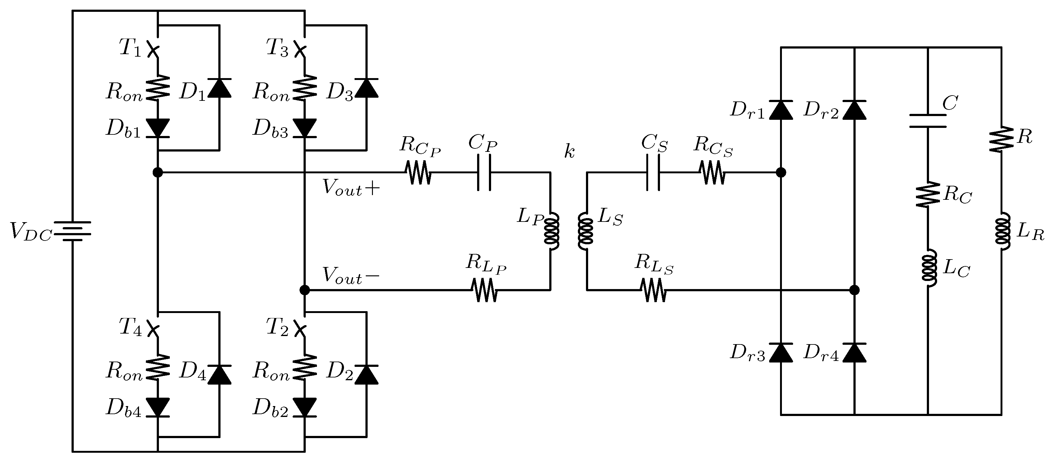
2. Circuit Analysis of an IPT System
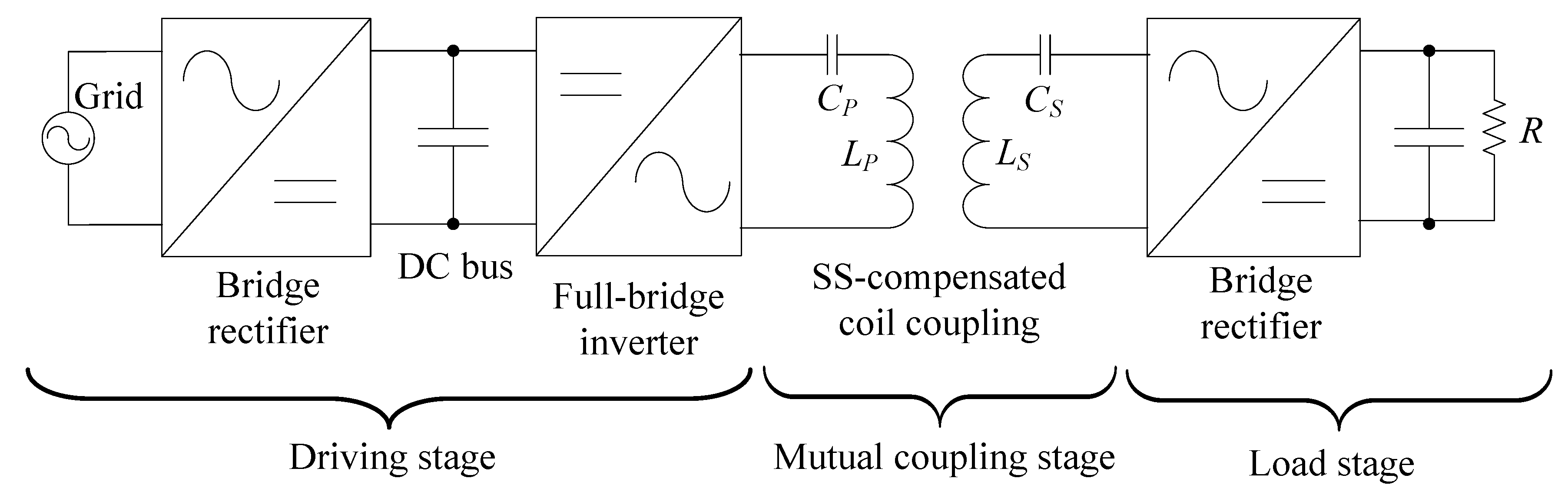
The general scheme of an IPT system comprises three stages: a primary section, supplied by a grid, followed by a compensated inductive coupling with a primary and a secondary coil and finally by a secondary section that charges a battery. The primary coil is driven by an alternating signal supplied by a full-bridge inverter located in the primary section. The voltage induced across the secondary coil is, in turn, rectified and conditioned prior to feeding the battery, sometimes with the insertion of a DC/DC converter or simply with a filter capacitor. The battery is usually replaced in laboratory prototypes with a variable resistor
R that reflects its state of charge (SOC) at a given time of the charging process [
1].
Figure 1 depicts the three stages particularized for the SS-compensated IPT prototype used in this work.
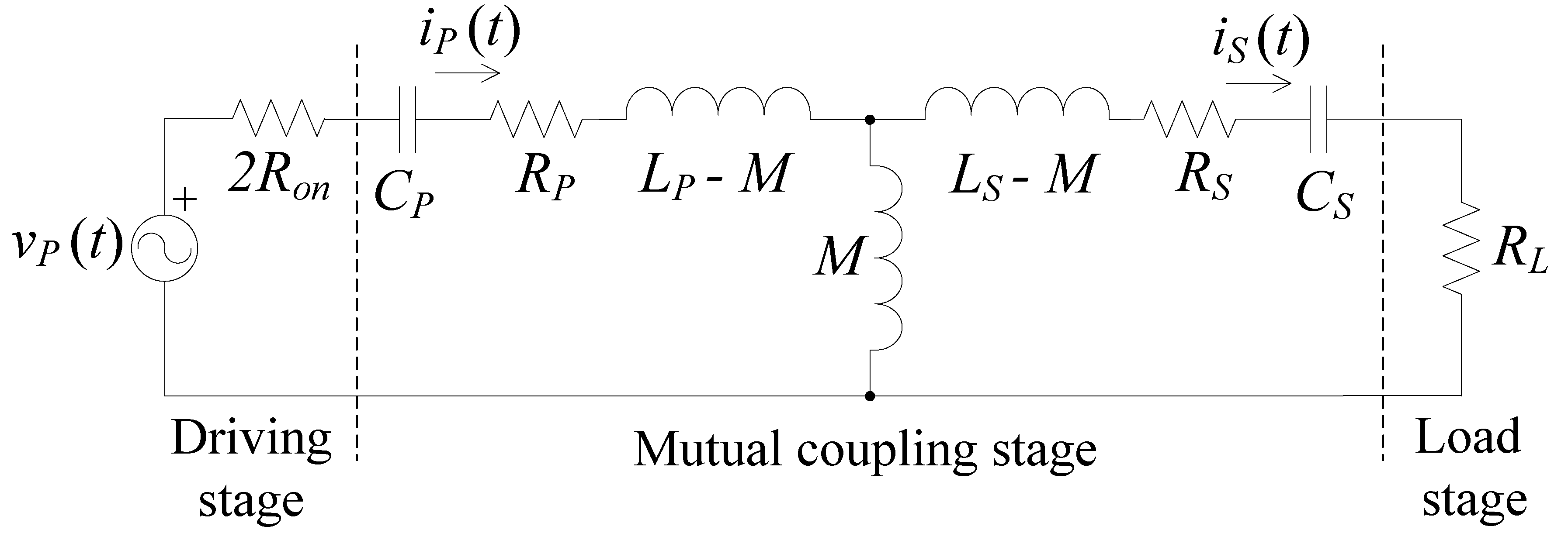
A simplified equivalent circuit of the entire IPT prototype is shown in
Figure 2. The circuit, which models the mutual coupling stage by means of a T-network, can be analyzed via a fundamental harmonic approximation (FHA) owing to the presence of a sinusoidal voltage source
that represents the fundamental component of the voltage that drives the primary coil generated by the inverter. FHA is a widely-used approach in the context of IPT systems that simplifies the analysis without compromising the accuracy, since the harmonic content of the resonant currents is usually low owing to the high quality factors of the resonant tanks [
18].
The conduction resistance of any of the four inverter switches is modeled with
. Since two switches are closed at any given time when an AC output is synthesized from a DC input, the circuit model includes the resistance
in series with the driving voltage. The resistance
results from the sum of two contributions located in the primary section and connected in series: the stray series resistance of the primary coil,
, and the stray series resistance of the primary capacitance,
. The resistance
is, in turn, the sum of the stray series resistances of the secondary coil,
, and that of the secondary capacitance,
.
accounts for the equivalent resistance of the rectifier stage and the battery.
M represents the mutual inductance between the two coils, which relates to
k and to the primary and secondary self-inductances
and
through the following expression:
Leakage inductances on the primary and the secondary sides,
and
, can be expressed as a function of either
k or
M and the primary to secondary turns ratio
:
Note that the inductances
–
M and
–
M that appear in the T-model coincide with
and
only if
r = 1. Expressions (
1), (
2) and (
3) show that IPT systems, for which
k is necessarily low, have non-negligible leakage inductances.
In the phasor domain, the impedance seen from the primary side,
, can be written as:
where
is the reflected impedance, which depends on circuit elements present on the secondary side:
Since the primary and secondary resonant circuits are designed to resonate at the same frequency, the common resonance frequency is given by:
When the circuit is driven at the resonance frequency, both the reactances on the primary side,
and
, and those on the secondary side,
and
, cancel each other out.
is thus simplified to an expression without imaginary part, where
and
represent the peak amplitudes of their corresponding voltage and current phasors:
On the other hand, the power delivered to the load stage, represented by
, is [
17,
18,
21]:
Finally, the efficiency of the mutual coupling stage can be calculated as follows: [
14,
17]:
3. Laboratory Prototype
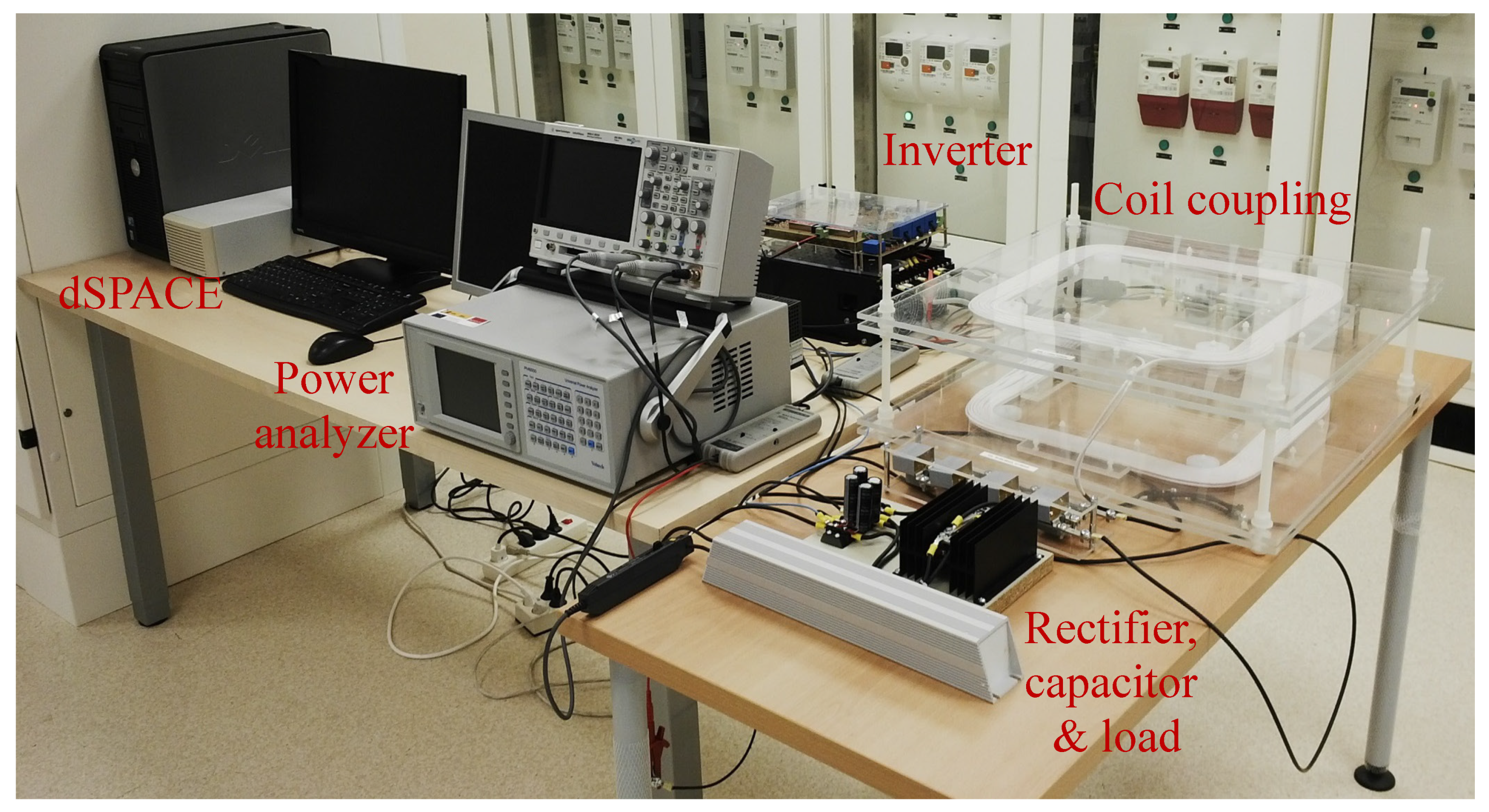
Figure 3 shows the three stages of the constructed prototype in a single image, along with the control electronics and the instrumentation utilized, all of which are described below.
3.1. Driving Stage
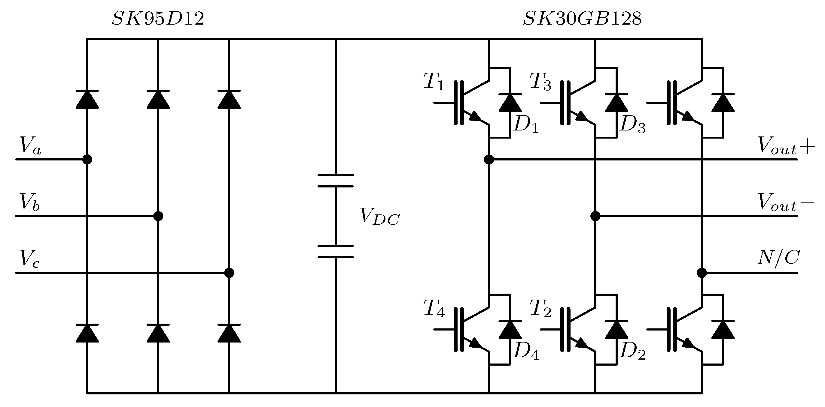
The driving stage, which was fed from a single-phase 230 V/50 Hz outlet of the power grid, features an AC/DC converter that provides a stable DC bus voltage
, followed by an H-bridge inverter based on IGBT switches. The driving function was implemented using two legs of a modular three-phase inverter connected to the grid, purchased from Semikron Electronics S.L., Barcelona, Spain. It includes a bridge rectifier (ref. SK95D12), an IGBT module (ref. SK30GB128) and some additional electronics.
Figure 4 depicts a simplified circuit diagram of the driving stage.
The bridge rectifier is characterized by a reverse voltage of 1200 V and a current of 95 A, whereas the IGBT switches support a collector-emitter voltage of 1200 V and a collector current of 25 A (all maximum ratings). Each of the two capacitors in
Figure 4 results from a parallel arrangement of four capacitors rated at 680
and 400 V. The equivalent capacitance of the eight capacitors amounts thus to 1360
and is rated at 800 V. The features of the driving stage were expanded by means of a customized PCB attached to the top of the inverter: this includes a fiber optic interface to allow communication with a dSPACE control platform, a measurement unit of both the inverter leg currents and the DC bus voltage, and a module to protect against overcurrents.
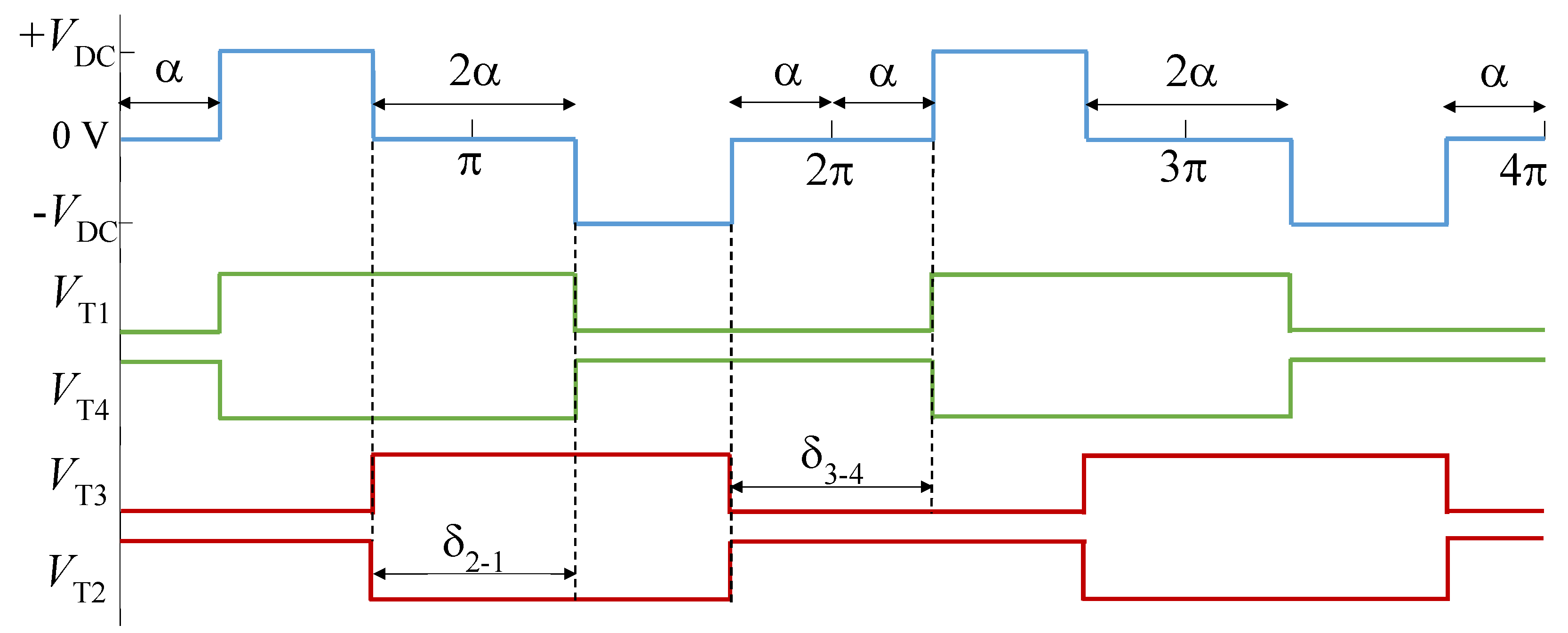
Although the H-bridge inverter is a single-phase two-level voltage-source converter (VSC), its switching scheme is such that it does not produce a square wave output voltage, but rather a controlled one with intervals in which the output is both zero and
and
. This controlled output with three output levels, whose duty cycle can be adjusted, is characteristic of a phase-shift control scheme. The inverter output voltage can be set to zero periodically during the so-called interval of zero voltage, whose duration can be regulated in the full range from 0 rad to
rad throughout each period. It is characterized by the zero-voltage angle
, which varies from 0 rad to
rad. As can be seen in
Figure 5, the trigger pulses
and
, which are applied to their respective IGBT gates located on the left leg of the inverter, are complementary. The same applies to the trigger pulses on the right leg,
and
. The four pulses have a duty cycle of 50%. The synchronization scheme results in a phase shift
between the pulses
and
, on the one hand, and a second phase shift
between
and
, on the other. Both of them are equal to
, whereas the interval of zero voltage is
throughout a period.
The amplitude of each harmonic that is present in the inverter output voltage waveform can be controlled by varying
, as stated in (
10) [
28].
The inverter output rms voltage
is, moreover, dependent on
[
28]:
The rms current supplied by the inverter to the primary coil can consequently be set to a given target value by simply selecting the appropriate angle
. An analog voltage, which is proportional to the
required, was generated by using a dSPACE 1103 (dSPACE GmbH, Paderborn, Germany) control platform. That voltage was, in turn, read by the IC UCC3895 (Texas Instruments, Dallas, TX, USA), a phase-shift PWM controller that generated the switching scheme shown in
Figure 3 and is required to synchronize the trigger pulses
to
. The resulting inverter output voltage had a frequency of 18.65 kHz. Examples of IPT systems with an SS compensation topology featuring a phase-shift control scheme are those described in [
14,
20,
29].
3.2. Inductive Coupling Stage with SS Compensation
Both circular and square coils have been reported in the construction of IPT prototypes. Considering that the mutual inductance
M between square coils is
times larger than between circular ones when the corresponding circumference is inscribed in the square [
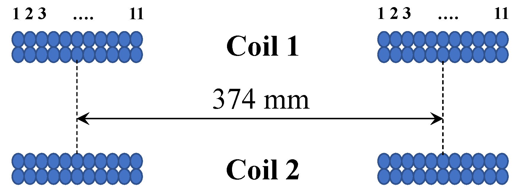
30], square rather than circular coils were chosen to design the coupling stage. The two coils, which were wound using Litz wire with a section of 6.28
, have 22 turns each with 11 turns piled up on top of the other 11, as
Figure 6 illustrates.
Mechanical stability was achieved by sandwiching each coil between two methacrylate plates. The air gap between the coils can be manually adjusted to the desired value by means of nylon screws placed at the corners of the holding plates. The four screws also contribute to keeping the coils perfectly aligned and parallel to each other.
Each of the two compensation capacitances resulted from an arrangement composed of four branches connected in parallel and two polypropylene film capacitors connected in series per branch, with a nominal capacitance of 100 nF per capacitor (ref. MMKP386 F1230 manufactured by Vishay, Malvern, PA, USA). This arrangement is necessary to support the high voltages developed across the capacitors when the prototype operates at the resonance frequency.
3.3. Load Stage
The load stage comprises a high voltage rectifier followed by a capacitor arrangement with which to reduce the ripple current, which is in turn connected to a combination of power resistors.
The bridge rectifier was constructed by connecting two semiconductor modules (ref. STTH6006TV, ST Microelectronics, Geneva, Switzerland) . Each module includes two ultrafast diodes characterized by a peak reverse voltage of 600 V and an average forward current of 30 A (absolute ratings).
The filter capacitance was the result of combining four electrolytic capacitors in an arrangement composed of two branches connected in parallel with two capacitors connected in series per branch. Each capacitor is rated at 220 and 450 V, with a capacitance tolerance of ±20%.
The power resistors utilized were of a wirewound type rated at 800 W. Ten different ohmic values, from 2.5 to 40 , were available from series and parallel combinations of resistors with a nominal resistance of 10 .
3.4. Prototype Testing and Performance Figures
Tests were conducted for three air gaps between coils (125, 150 and 175 mm), which will henceforth be referred to as
, where
x is the corresponding gap. The rms primary current,
, was kept at approximately 10 A via individual adjustments of the angle
for each air gap
and resistance
R being tested. Controlling the current in the primary coil allows the series-compensated secondary side to resemble a voltage source [
9].
The load power
depends strongly on both
and
R. For
, the air gap for which the magnetic coupling is the strongest of all three,
reached 2 kW when
R was 5
(higher loads led to lower transferred powers). On the other hand, if the three air gaps are considered altogether,
was always above 1 kW for
R = 5
and below 500 W for
R = 30
. The overall efficiency, computed from grid supply to load, was 82.5% for the intermediate case of
. However, if only the coil coupling stage is taken into account, it exceeded 90%. Further details regarding the prototype performance can be found in [
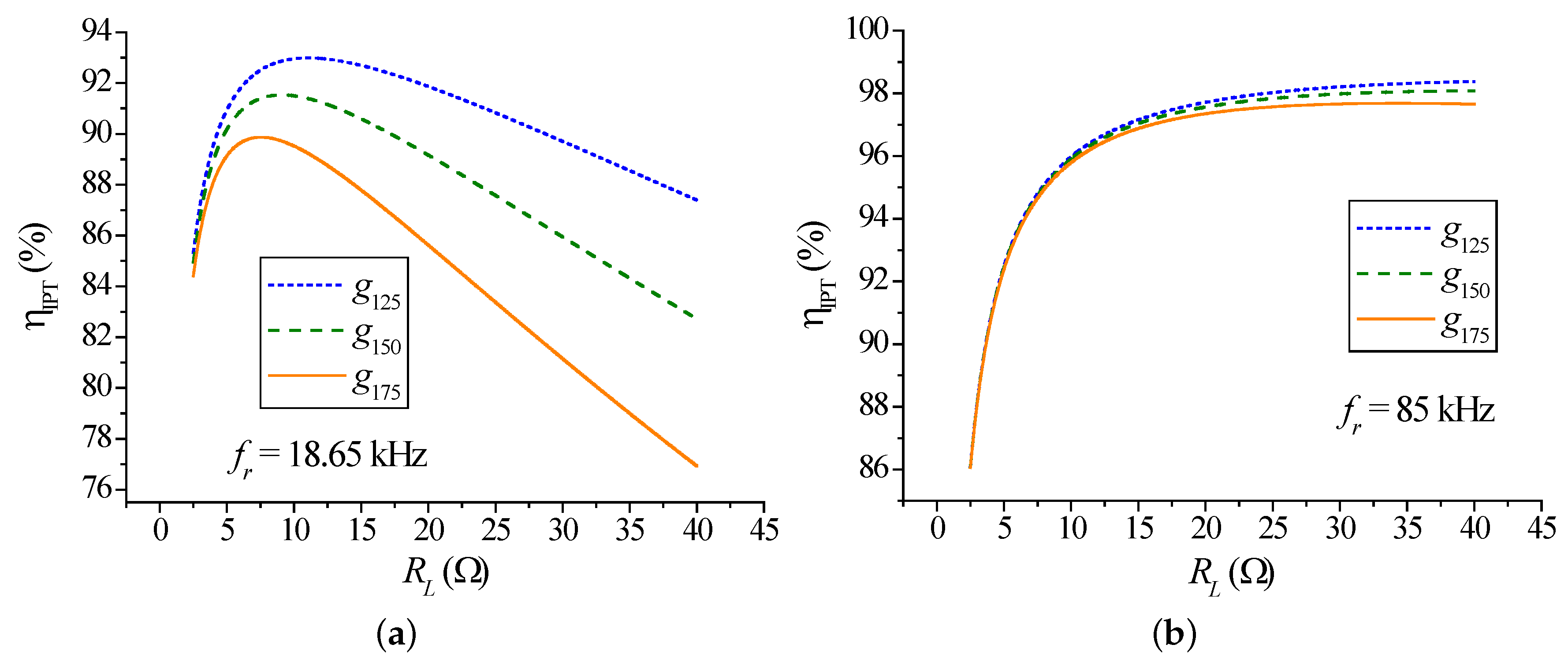
14]. It should be noted that, according to (
9) , the efficiency of an SS-compensated inductive coupling stage depends, among other parameters, on the resonance frequency
and the mutual inductance
M, and an increase in either of them causes an increase in the efficiency.
Figure 7 plots
calculated with (
9) for the three air gaps and two different resonance frequencies (18.65 kHz and 85 kHz), with the load resistance
ranging from 2.5
to 40
. As can be seen, when the frequency is 18.65 kHz,
is above 90% only under certain operation conditions, in agreement with the efficiency figures found experimentally. However, for the case of 85 kHz,
represents a significant improvement, exceeding 95% for most of the loads and air gaps. Unfortunately, the desired increase in
that arises as a consequence of an increase in either
M or
is accompanied necessarily by a reduction in the power delivered to the load, as follows from (
8). Consequently, an IPT system working at a relatively low frequency of operation, as in the case discussed in this work, is characterized by moderate efficiency figures that are compensated by an enhanced power transfer capability.
4. Experimental Determination of the Coupling Factor
A reliable figure for the coupling factor between two coupled coils can be obtained experimentally by applying the voltage ratio method, which consists of measuring the peak amplitude of the voltage waveform at each winding in open circuit conditions when a sinusoidal driving voltage is applied to the other winding [
31]. The method, therefore, requires four voltage measurements for a given air gap between coils: the driving voltages at the primary and secondary windings, denoted by
and
, and the corresponding open circuit voltages, represented by
and
. Since the accuracy is improved if measurements are taken at a frequency at which the quality factor
Q of the coils is high [
31], the selected frequency of the driving voltage was 20 kHz. The experimental coupling factor obeys the following expression:
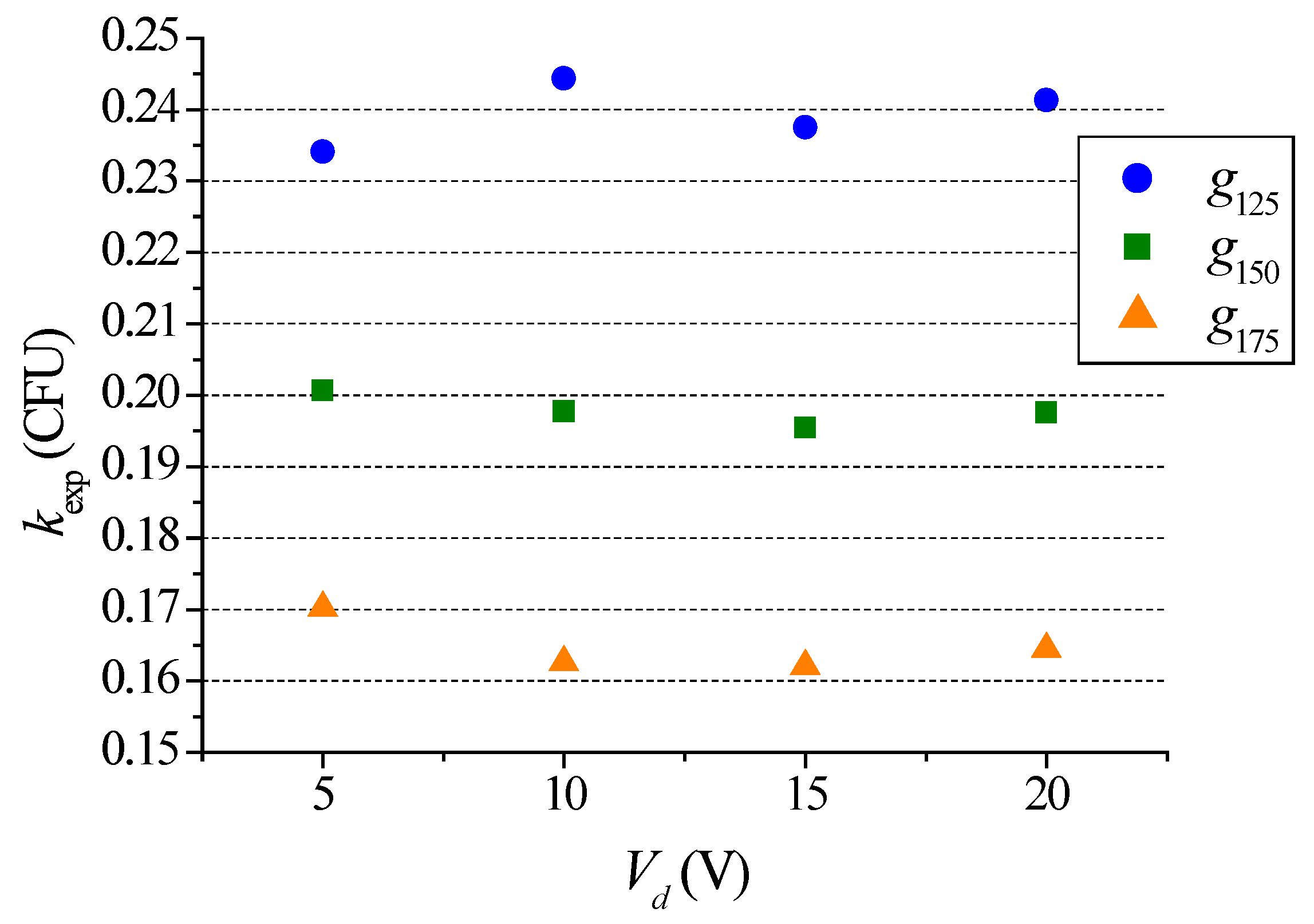
Considering that, for a given amplitude of the voltage applied to the driving coil, the voltage across the open-circuited coil decreases as the air gap increases, the presence of noise on the voltage signals can compromise the accuracy of the measurements, especially in the case of large air gaps. Small driving amplitudes were, therefore, avoided. In order to verify whether or not there is a threshold for the driving amplitude below which the
k values obtained lack accuracy, four sets of measurements were taken for each air gap, during which the driving amplitudes
were set to values of around 5, 10, 15 and 20 V. The resulting
k values are represented in
Figure 8.
As can be seen, the method is able to distinguish among the three cases under study satisfactorily for every
. However, there is a noticeable upward deviation of the
k factor obtained for
when
is 5 V with respect to the values that result from the other three amplitudes, which are not that different from each other. A similar deviation for 5 V, although more moderate, occurs for
. The same occurs with
, this time with a downward deviation. This analysis suggests that the driving voltage threshold sought is located somewhere between 5 and 10 V and measurements at 5 V were consequently ruled out. Although the remaining sets of measurements taken at 10, 15 and 20 V gave rise to similar
k factors, the 20-V set can be regarded as the most reliable of all as its signal-to-noise ratio is the largest. The
k values obtained with that set are represented in
Table 1 and will be used as targets to be compared with the corresponding values resulting from the simulations.
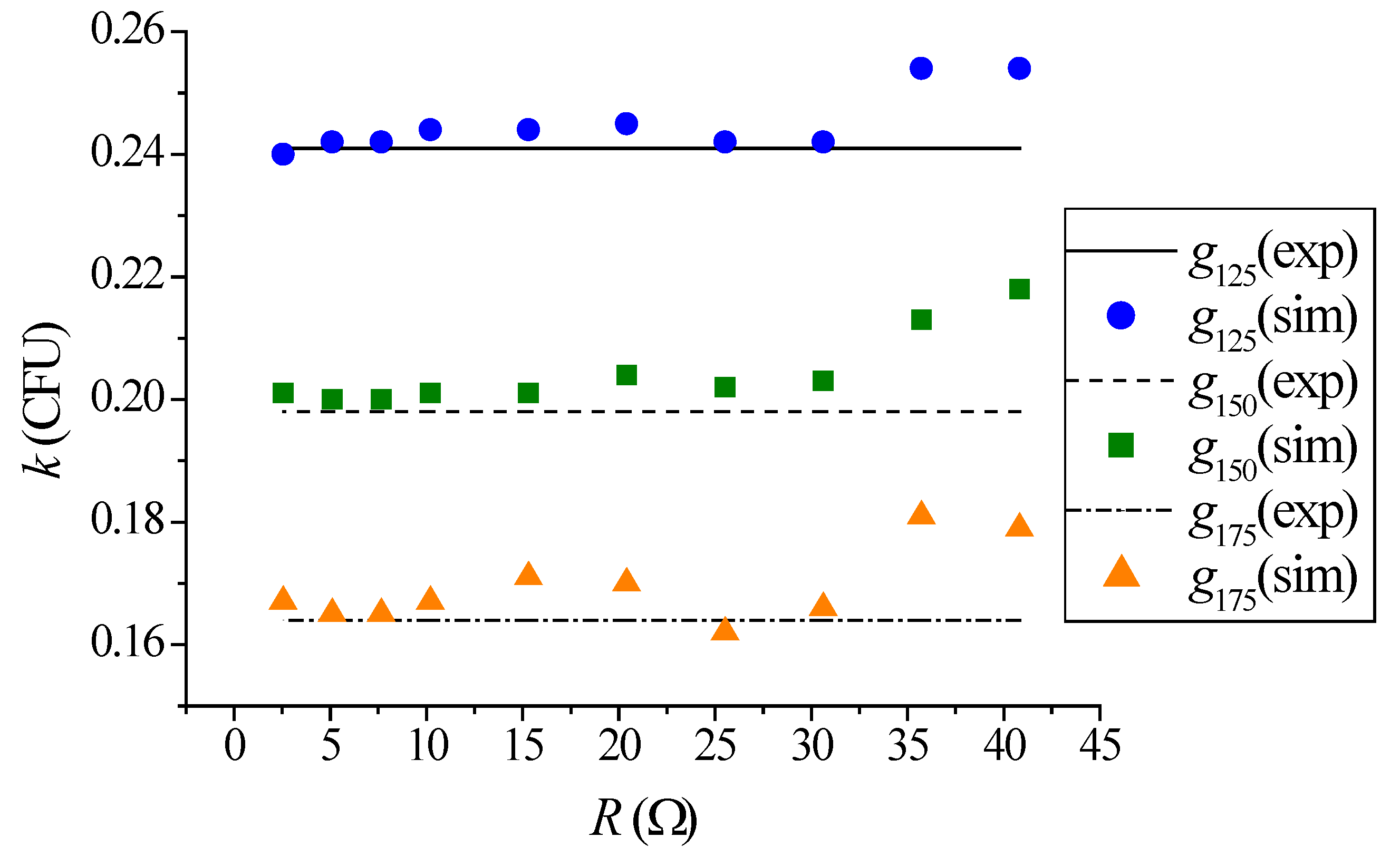
6. Model Validation
Six input parameters had to be confirmed prior to running a simulation: the DC bus voltage
, the switching frequency
f, the zero-voltage angle
, the load resistance
R with its series stray inductance
, and the coupling factor
k. Simulations for each air gap were run with ten different load resistances, whose nominal values were 2.5, 5, 7.5, 10, 15, 20, 25, 30, 35 and 40
. All possible combinations of different loads and air gaps led to a total of thirty angles
with which to keep
controlled at around 10 A. Several
k values were tentatively tried for all combinations of
and
R until the best match between the experimental and the simulated primary peak currents was found, using three decimal digits for
k. Following this iterative procedure for every combination of
and
R yielded a set of ten
k values for each air gap. The results, which are compared with the experimental
k values in
Table 1, are shown in
Figure 10.
Upon inspecting
Figure 10, it is apparent that the model is capable of discriminating well among the three air gaps, although deviations from the expected
k values are especially noticeable for the loads of 35 and 40
. As a result of the phase-shift control action,
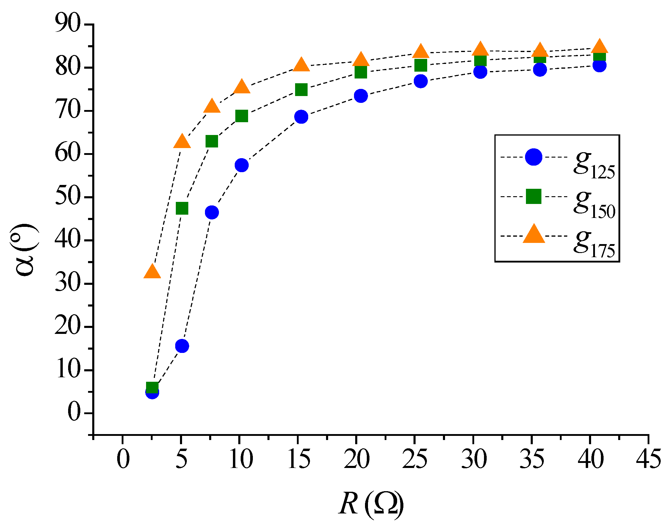
adopts new values as the whole range of loads is swept.
Figure 11 shows that
converges to 90
as
R increases, regardless of
. This increase in
with
R makes the rms voltage at the inverter output drop in order to keep the primary current controlled for every load, as follows from (
7) and (
11). In practice, after a new load was connected,
was adjusted manually from the dSPACE platform until the monitored
was as close as possible to 10 A.
As a consequence of this gradual convergence process, the rate at which
changes has a non-linear dependence with
R: a given increment in
R makes
undergo a significant increase in the area of small loads; however, the same increment causes only a moderate increase in
for large loads. Although this holds for the three
, the effect becomes more pronounced as the air gap increases. Note that the cosine function in (
10) accounts for the non-linear behavior observed.
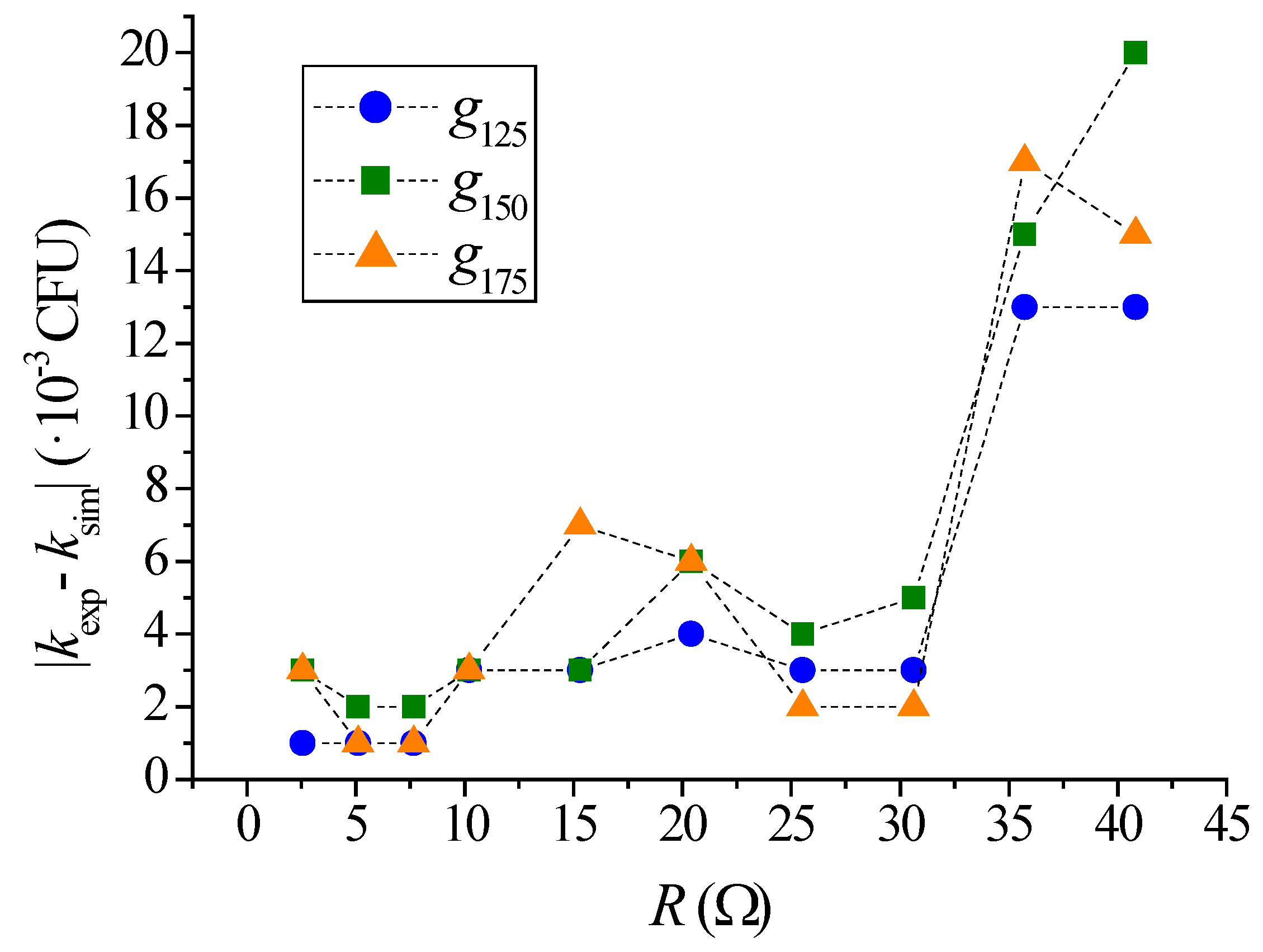
The deviations from the experimental
k factors, expressed in coupling factor units (CFU), are plotted in
Figure 12 in the form of absolute errors. They reach a maximum of
CFU with the exception of the two cases mentioned previously, in which they grow remarkably larger. Overall, the area of low
R (up to 10
) behaves best, as the deviations are
CFU or less for the three
. It should be noted that the absolute errors found for
are the smallest for the ten loads, ranging from
to
CFU with the exception, once again, of the two largest load resistances.
The accuracy of every single model parameter contributes to the reliability of the circuit model, even in the case of those parameters that, in principle, play a minor role. This is the case of
: if, for a given
and
R,
decreases from its actual value of 48
to 1
(that is, the inverter switches are modeled as virtually ideal devices), the primary peak current increases according to (
7), which in some cases alters the
k obtained with the circuit model. Taking for example
, the increase in the primary current caused by that drop in
does not suffice to modify
k for
R = 2.5
. However, in the case of R = 40
,
k undergoes an increase of
CFU, which would add to the corresponding absolute error, making the deviation from the experimental
k even larger.
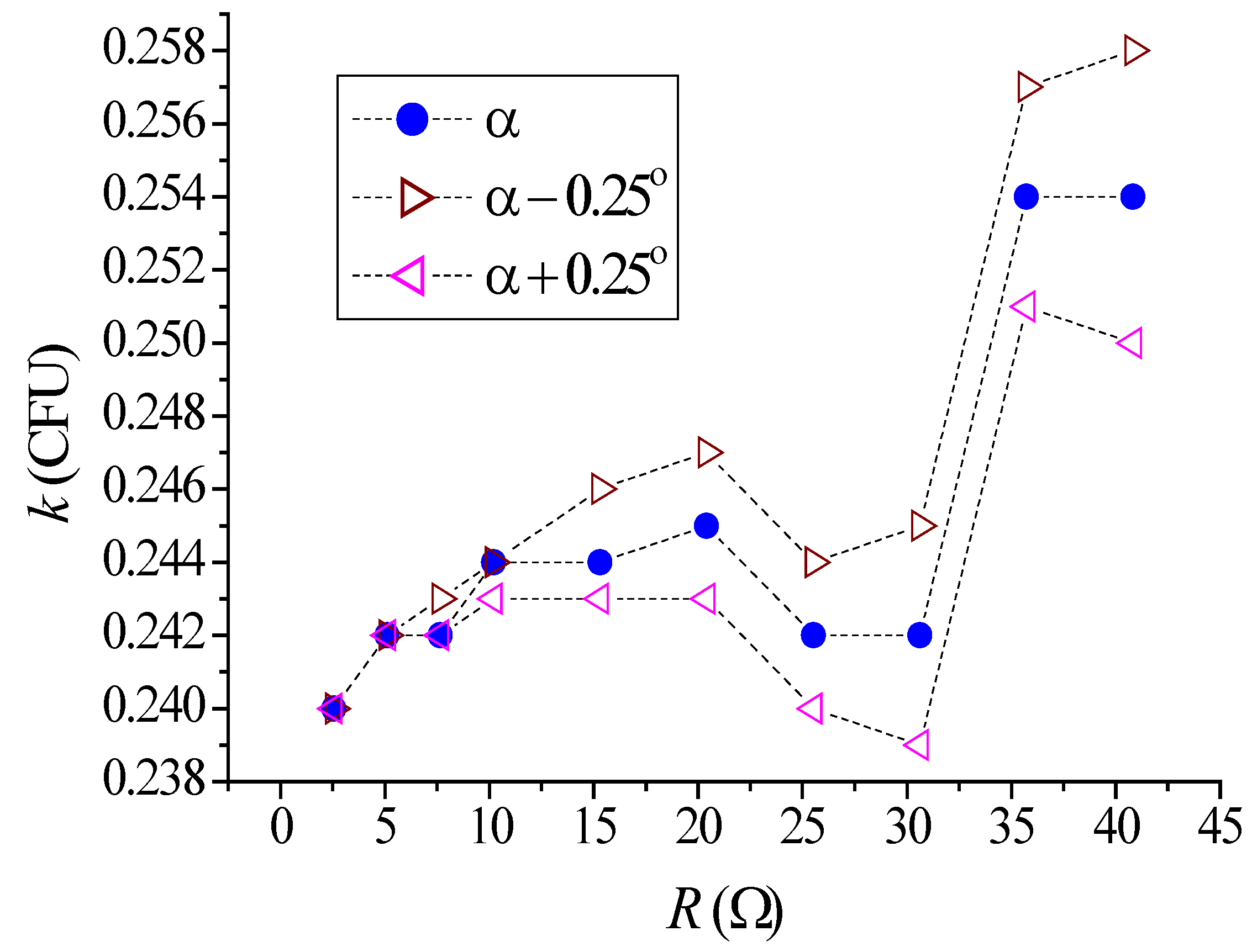
As stated previously, an increase in R translates into small increases in in the area of high loads. This has important implications with regard to the sensitivity of the system and its capability to accurately determine k, since a small change in when the prototype is loaded with a large R leads to significant variations in the peak primary current. It is, therefore, of interest to test the model response under small variations in that may occur owing to a measurement error, as results from time measurements of the experimental waveforms of the inverter output voltage.
Assuming that
was obtained with an error of
, and plotting
k against
R for
for illustration purposes, it is apparent that
k undergoes an increasingly larger shift from the
k factors obtained with
as
R increases. As can be seen in
Figure 13, the error has little or no influence on
k within the low load range. However, from 10
onward, the shifts grow larger and larger both above and below the initial
k values, reaching a maximum of
CFU for 40
(
k = 0.250 for
+ 0.25
and
k = 0.258 for
− 0.25
). If a small measurement error in the determination of
is taken into account, the capability of the system to deliver reliable figures for
k consequently worsens as
R increases. This may contribute to justifying the deviations found in the determination of
k for the two largest loads.
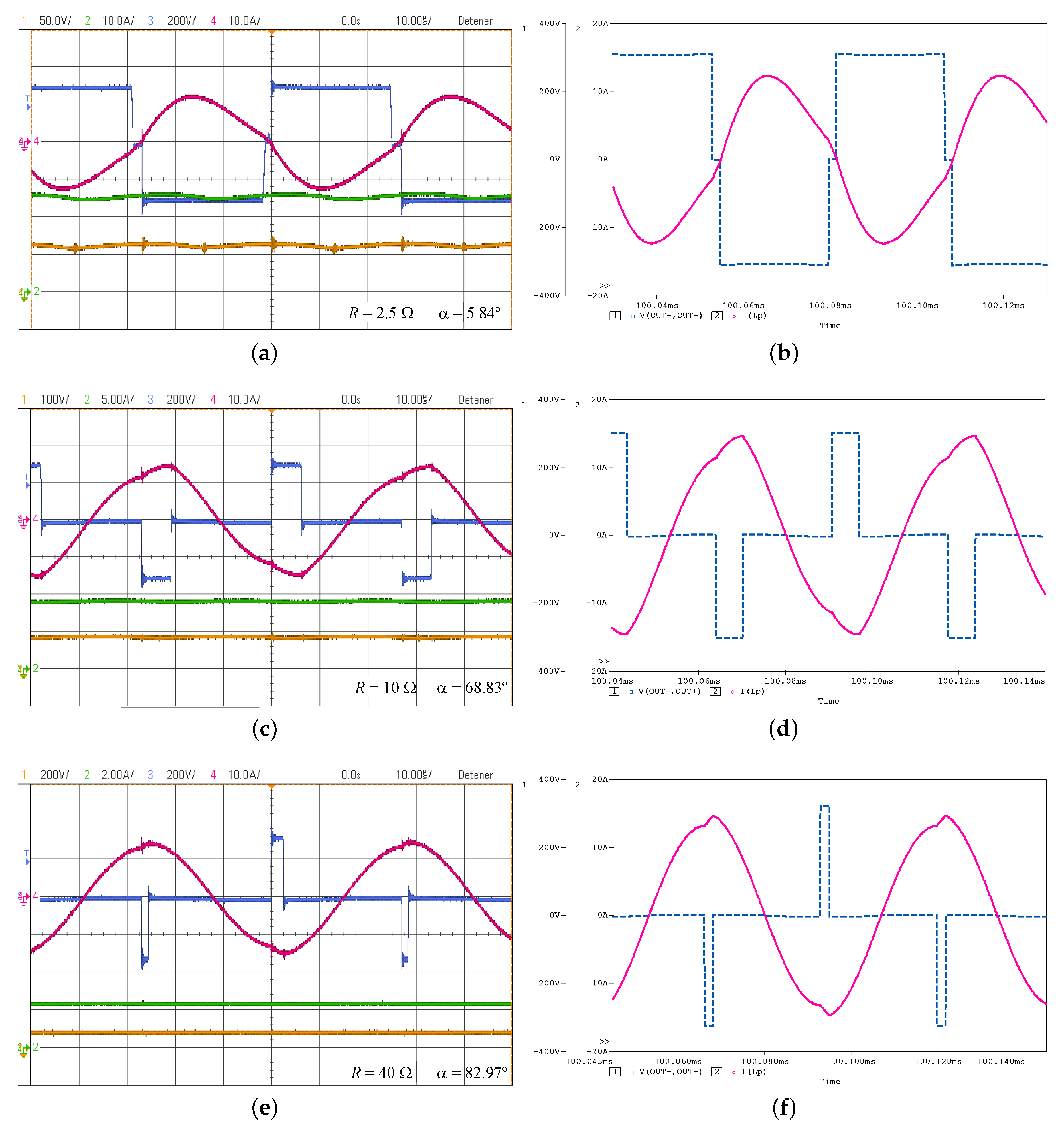
7. Waveform Analysis
Both experimental and simulated waveforms are shown in
Figure 14 for comparison purposes. The inverter output voltages and currents are represented by blue and pink lines, respectively. A selection of three representative cases was chosen (specifically, those corresponding to 2.5, 10 and 40
for the intermediate air gap
). Note that the duty cycle of the inverter output voltage is very low for 40
, one of the two cases in which the circuit model behaves worst.
A comparison of the shapes and amplitudes of the two sets of waveforms makes it possible to conclude that the simulated waveforms are very similar to their experimental counterparts. Moreover, the shape of the current waveforms is quite sinusoidal in all cases, which confirms the validity of the FHA approximation adopted before analyzing the equivalent circuit of the IPT prototype. The low harmonic content of the primary current waveforms can be understood in terms of the band-pass filtering process introduced by the resonant circuit on the primary side of the coupling. Alternatively, it can be regarded as a consequence of dealing with loosely coupled coils, which are characterized by a low
k. Recall that leakage inductances are, according to (
2) and (
3), relatively large in the circuit model of a weak inductive coupling: a large leakage inductance effectively filters out most of the harmonic content of the current waveform, leading to the observed sinusoidal-like waveforms. Furthermore, the larger the air gap is, the larger the leakage inductance becomes, and more frequencies are consequently rejected from the spectrum of the current waveform. This effect is illustrated in
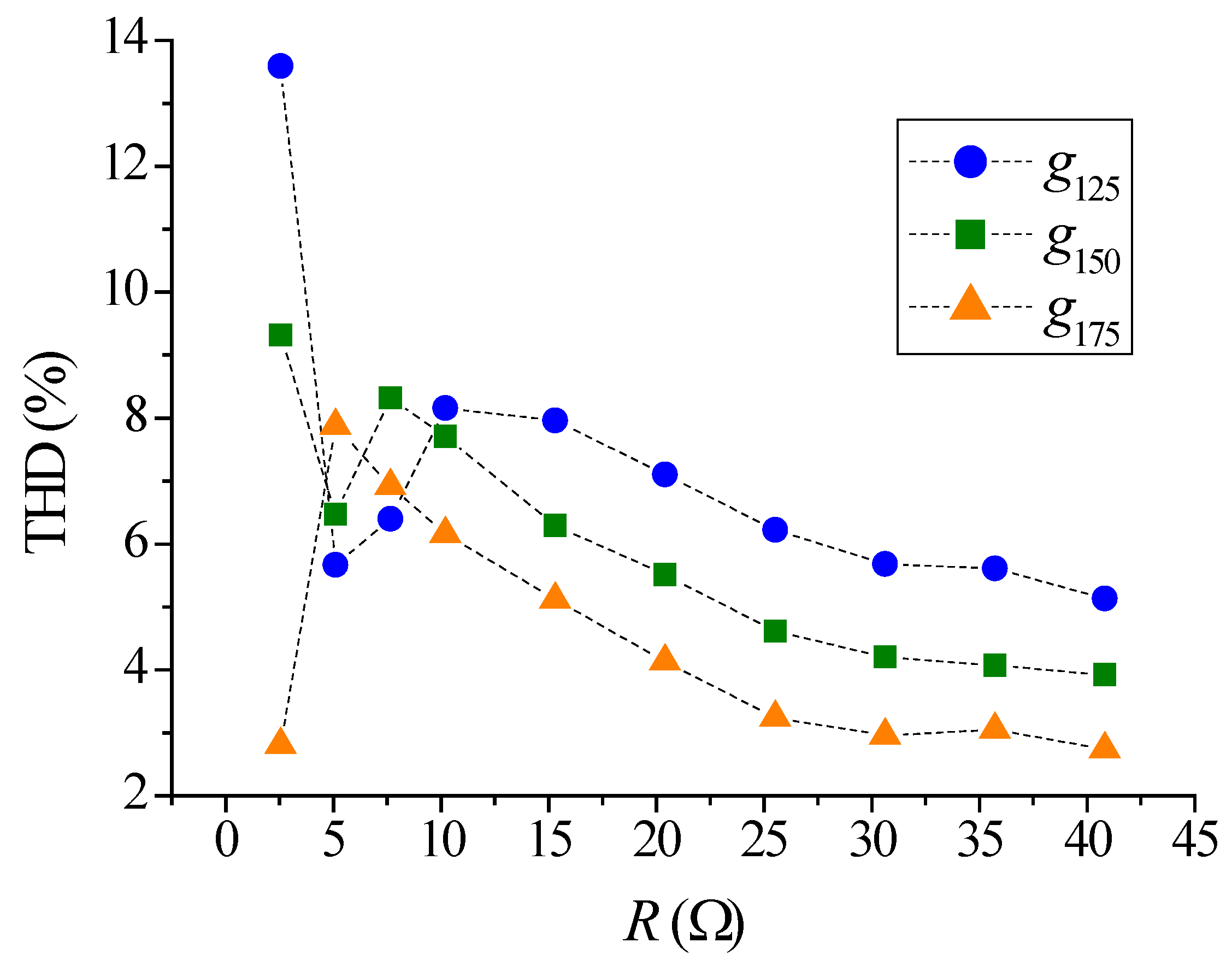
Figure 15, which represents the total harmonic distortion (THD) versus
R. As can be seen, the harmonic content decreases as
increases, which is easier to verify for those loads in which
is similar for the three
(all of them, with the exception of the three smaller ones). In the case of small loads (up to 10
), the plot does not show the effect clearly since, for a given load, the corresponding three angles
are quite different depending on
. Finally, it should be pointed out that no correlation was found between the harmonic content and the deviations in
k depicted in
Figure 12. In fact, the THD is especially low for the two largest loads, for which the model behaves worst. It is not, therefore, possible to claim that the two estimates of
k with the largest absolute errors occur as a consequence of a high harmonic content in the corresponding current waveforms.
8. Conclusions
A PSpice circuit model, developed as a replica of a 2-kW IPT charger operating at 18.65 kHz and controlled with the phase-shift technique, has been tested and validated for three air gaps of practical interest in the case of light-duty EVs: 125, 150 and 175 mm. The validation procedure was based on determining the existing deviations between the coupling factors obtained experimentally for every air gap and those delivered by the simulation model for a set of ten load resistances, ranging from 2.5 to 40 . The results show that the deviations are within reasonable limits (below CFU) for the three air gaps and all the loads tested with the exception of the two largest, for which the duty cycle of the inverter output voltage is especially low and accuracy is, therefore, compromised. The best agreement was found in the lower range of load resistances (up to 10 ), in which deviations lie between CFU and CFU. Consequently, the overall performance of the simulation model is satisfactory, although there is evidence of a certain threshold level for the load resistance (or, equivalently, for the zero-voltage angle ) above which the reliability of the simulation model declines. Setting the threshold at the nominal resistance of 35 , the corresponding angles are , and for the air gaps of 125, 150 and 175 mm, respectively. Since one of the six input parameters of the circuit model is the switching frequency, the PSpice circuit developed can be readily adapted to simulate the behavior of prototypes that comply with the SAE-J2954 standard issued for EV wireless charging, which establishes a nominal switching frequency of 85 kHz.


