A Dual-Band Compact Metamaterial Absorber with Fractal Geometry


DIMES - Università della Calabria, 87036 Rende, Italy
*
Author to whom correspondence should be addressed.
Electronics 2019, 8(8), 879; https://0-doi-org.brum.beds.ac.uk/10.3390/electronics8080879
Submission received: 9 June 2019
/
Revised: 21 July 2019
/
Accepted: 6 August 2019
/
Published: 8 August 2019
(This article belongs to the Special Issue Engineering Metamaterials)
Abstract
:A fractal absorber based on a metamaterial configuration is proposed for dual-frequency operation within the UHF band. The miniaturization skills of the proposed fractal shape are used to design a dual-band metamaterial absorber cell with reduced size (<λ/2 at the two operating frequencies) and a very thin substrate thickness (≅λ/100). A metamaterial absorber panel is realized and experimentally validated. Good agreements between full-wave simulations and measurement results are demonstrated.

1. Introduction
Electromagnetic absorbers are usually adopted to reduce unwanted reflections of an impinging wave within a prescribed frequency band. Several types of electromagnetic absorbers have been developed in literature [1,2,3] for various applications throughout the electromagnetic spectrum. Among the above designs, metamaterial absorbers (MAs) have been proposed in Reference [2] as giving small-volume and low-cost absorbing structures. They are composed of a set of periodic resonant metallic patches on a grounded dielectric layer. MAs can be properly synthesized to perform ideal absorption in the neighborhood of a given frequency. Since their first presentation [2], MAs have been employed in various applications [3], such as electromagnetic interferences reduction, multi-path mitigation of indoor RF-applications, and electromagnetic compatibility enhancement of electronics devices. Recently, MAs have been also proposed to operate at low microwave frequencies, usually requiring much more cumbersome absorption structures. In particular, some MA configurations have been designed in References [4,5,6,7,8] to improve the robustness of RFID systems working in the Ultra High Frequency (UHF) range.
In this paper, an ultra-thin fractal MA cell, first illustrated by the authors in Reference [9], is presented for dual-band operation within the UHF range. Even if other dual-band/multi-band MA configurations can be found in literature [10,11,12,13,14,15,16,17], this is the first example working at UHF frequencies. Unlike other multi-band MAs [10,11,12,13,14,15,16,17], the proposed fractal MA-cell allows to achieve closer absorbing peaks. Furthermore, the adopted single-layer structure offers reduced thickness (≅λ/107) and very small unit cells (≅0.4λ), with λ being the free-space wavelength at the smaller resonant frequency. In order to provide a preliminary experimental validation of the proposed absorber configuration, a MA panel operating within the UHF-band is tested. Very low reflection coefficient values (≤−22 dB) are detected, under normal incidence, at both operating frequencies, thus providing very high absorption rates (≥99%) in dual-band operation.
2. Dual-Frequency Fractal Unit Cell
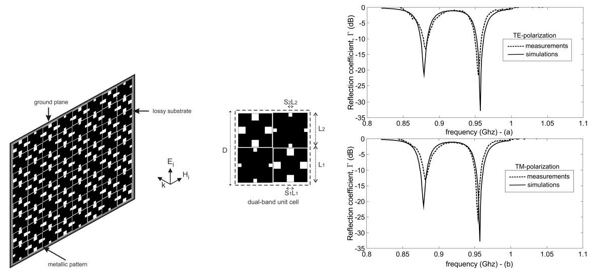
The dual-band MA structure proposed in this paper is illustrated in Figure 1, where the black fill part is a conductor (35 µm-thick copper). It consists of fractal cells periodically distributed and printed on a thin grounded dielectric layer (Figure 1). The MA-unit cell is composed of two alternately arranged couple of Minkowski patches (Figure 1), each one synthesized to work in the neighborhood of a specific resonant frequency. The proposed MA structure is backed by a metallic sheet (i.e., the ground plane in Figure 1). For this reason, there is no transmission through the absorber panel, so we only need the MA reflection response (Γ) to correctly compute the absorption (i.e., A = 1 − |Γ|2) of the proposed structure.
The Minkowski fractal geometry, yet proposed by the authors in Reference [7] for designing a single-frequency UHF MA-cell, is composed by a starting L × L square element, which is properly changed by eliminating a smaller SL × SL square from the center of its sides. S is the scaling factor, varying from 0 up to 1/3.
The above fractal configuration allows to host an electrically longer resonator into a smaller unit cell [18,19], thus offering very appealing miniaturization skills. As a matter of the fact, the combined use of a smaller patch length L and a greater S-value allows to move down the patch resonance frequency, f0. This last parameter, in fact, is inversely proportional to the effective side length Leff of the patch (i.e., f0 ~ 1/Leff), which is approximately equal to Leff = (1 + 2S) L [8]. So, the longer the effective fractal side is, the smaller the resonant frequency will be. Furthermore, in order to realize the perfect absorption condition at the desired resonant frequency f0, both degrees of freedom of the adopted Minkowski shape, i.e., the length L and the inset size SL, can be exploited. In other words, the fractal sizes must be chosen to match the MA unit cell impedance, Zcell, with the free-space impedance ξ0 = 377 Ω, in correspondence of the design frequency f0 (i.e., |Γ(f0)| = , with Γ the reflection coefficient of the unit cell, see Figure 2a).
As demonstrated in the following, the proposed two-degree-of-freedom design technique simplifies the synthesis of a perfect MA-cell, giving simultaneous absorption and resonance conditions at the desired frequency, by tuning both fractal parameters L and S. Furthermore, the proposed geometry can be easily scaled to operate at different frequencies.
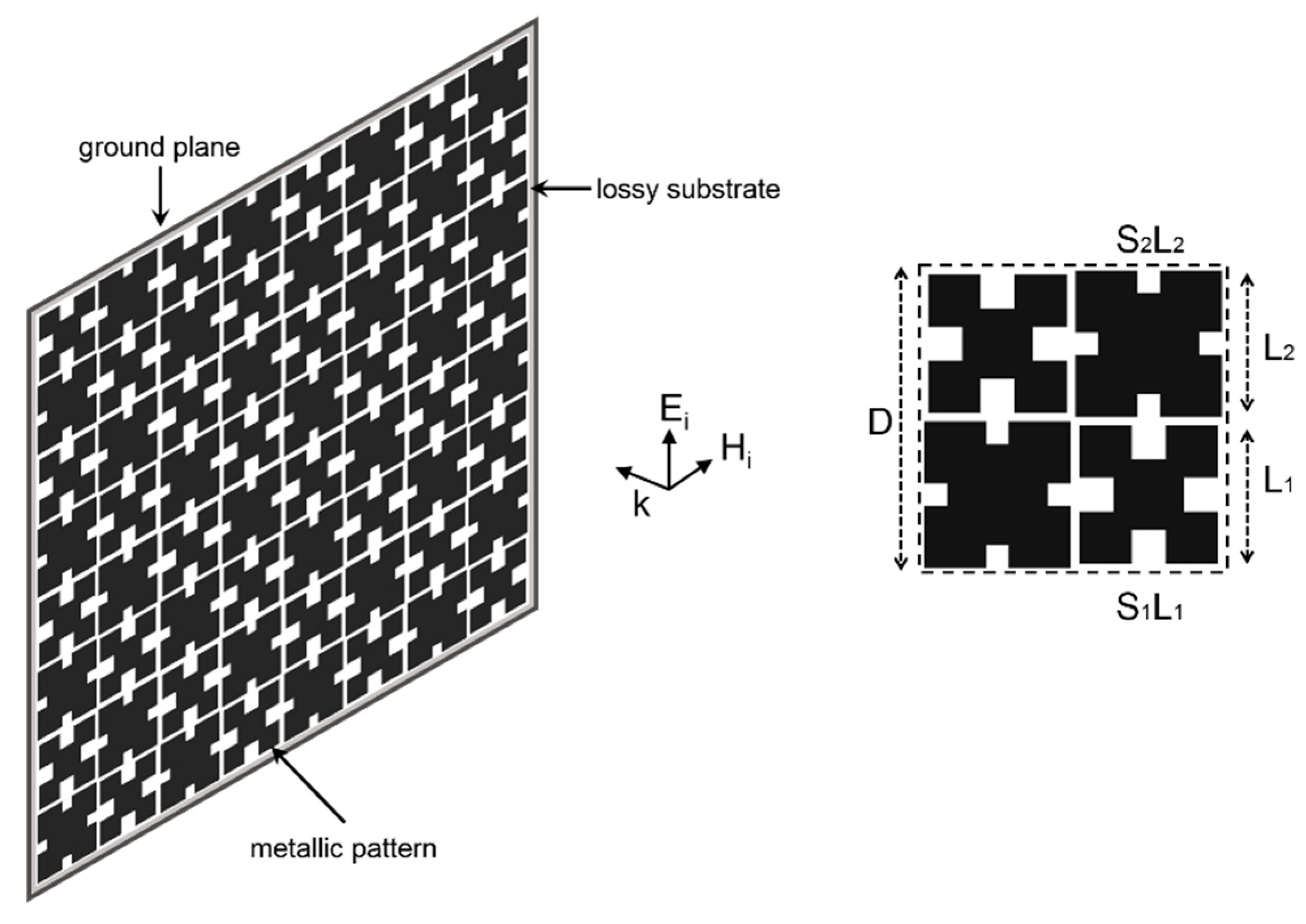
A test case demonstrating the above considerations is illustrated in Figure 2a. It represents the simulated reflection coefficient of a set of 868 MHz fractal MA cells, with progressively reduced sizes D, ranging from 0.3λ down to 0.15λ, with λ being the free-space wavelength. A commercial full-wave code is adopted (i.e., Ansoft Designer) by imposing the infinite periodic array boundary conditions.
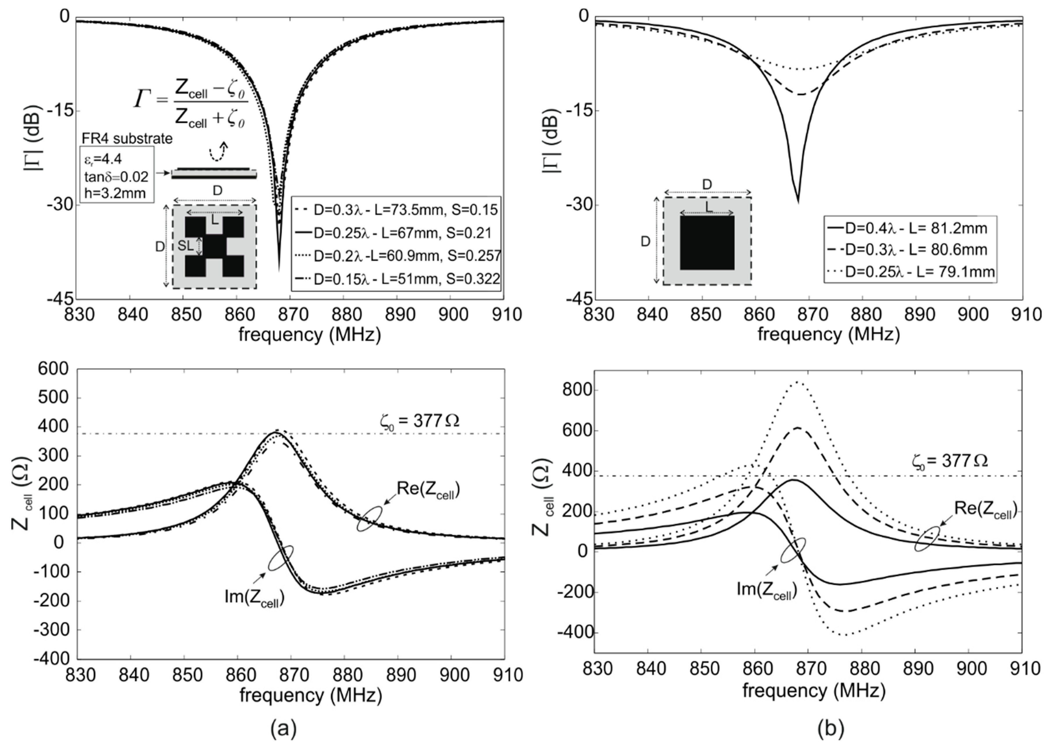
Results reported in Figure 2 show that a proper tuning of parameters L and S is able to guarantee an ideal absorption condition in all considered cases (i.e., |Γ(f0)| ≅ 0, namely A(f0) > 99% at f0 = 868 MHz, with A(f) = 1 − |Γ(f)|2). In fact, even if the use of cell size D of reduced dimension forces smaller patch lengths L (Figure 2a), the use of greater values for the scaling parameter S allows to have a patch with an increased electrical length, thus giving a downshift of the resonance condition with respect to the desired working frequency f0 = 868MHz (Figure 2a). From a physical point of view, the above behavior can be justified by the fact that the current path on the fractal patch is bent in correspondence of the inset SL (see Figure 3), thus the actual resonance length of the patch results to be lengthened by the SL notch.
For the above reasons, the adopted fractal geometry allows to design more compact unit cells: for the examples depicted in Figure 2, a size reduction of about 63% is achieved with respect to the conventional square-shaped MA cell, printed on the same substrate (see Figure 2b).
Moreover, Figure 2b illustrates how the reflection coefficient Γ(f0) of the unit cell relative to the square-shaped MAs increases when a smaller unit cell size D is considered, thus leading to a nonoptimal absorption. This behavior is due to the fact that the synthesis of a square-based MA-cell is based on the use of only one degree of freedom, i.e., the patch length L that is commonly chosen to fix the unit-cell resonance at the design frequency f0. No degree of control over the unit cell impedance is available, which instead depends on the following preset parameters: the unit cell size D, the resonant patch dimension L, and the substrate features (i.e., thickness, dielectric constant, loss tangent). As a matter of the fact, in the case of the square-based cells depicted in Figure 2b, the use of a smaller array grid spacing leads to a larger resonant input impedance value (i.e., Re(Zcell)), mainly due to the higher capacitive coupling between adjacent patches [8,20] that causes a progressively mismatching and a consequent reduction of MA absorption abilities (Figure 2b).
The above miniaturization capabilities are exploited in this paper to realize a dual-band feature by simply including two couples of fractal resonators in the same cell. The design process of the proposed dual-band cell follows the design rules described in Reference [8] for the case of a single resonant MA. Each fractal patch is synthesized to realize and ideal absorption, i.e., to have a matching condition between the impedances relative to the MA cell and that of free space [8] at the design frequencies f1 and f2 (i.e., |Γ(f1)| ≅ |Γ(f2)| ≅ 0).
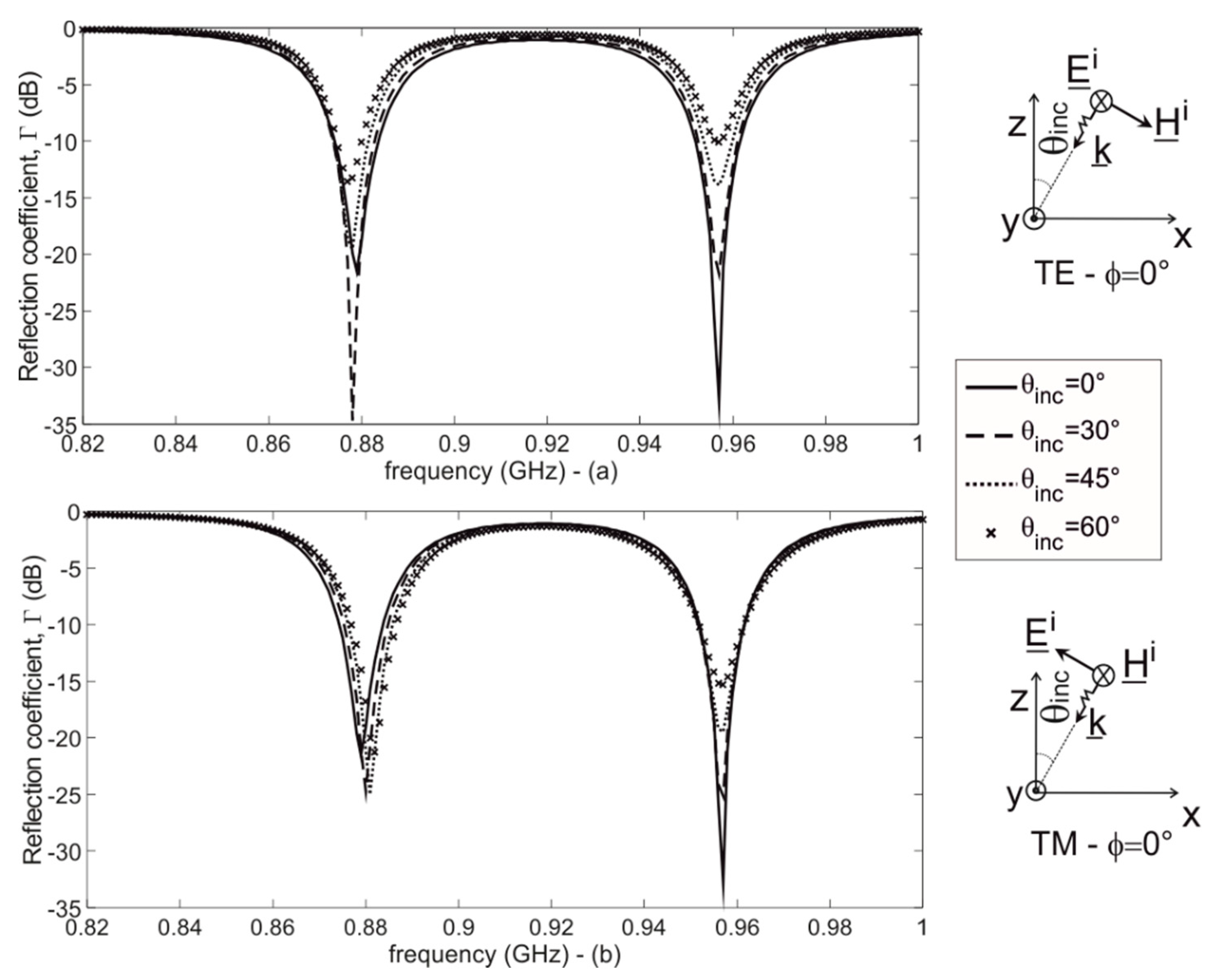
A MA unit cell, printed on a FR4 substrate (εr = 4.2, tanδ = 0.015, h = 3.2 mm), is designed by adopting the layout depicted in Figure 1. A commercially available full-wave code, based on the infinite array condition, is applied, with an assumed normal incident plane wave (θinc = 0°). As demonstrated in Figure 4 (computed reflection coefficient of the cell), two reflection nulls are achieved (i.e., |Γ(f1)| ≅ −22 dB, |Γ(f2)| ≅ −33 dB) at the following UHF-frequencies: f1 = 878 MHz and f2 = 956 MHz. The above nulls correspond to a pair of absorption peaks, A(f1) and A(f2), greater than 99%. The synthesized MA cell is characterized by the following dimensions: (L1, S1) = (64.2 mm, 0.245), (L2, S2) = (68 mm, 0.155), D ≅ 0.4λ, where λ is the free space wavelength at the lower frequency f1. As a further analysis, good angular stability is demonstrated for both TE (Figure 4a) and TM (Figure 4b) polarizations up to θinc = 60°. To this end, the reflection coefficients vs. frequency are computed for different incidence angles θinc.
Figure 4 shows a little frequency shift in correspondence of the first resonance, in the case of a TM polarization. Moreover, a reflection amplitude ranging from −34 dB up to −14 dB, at f1 (i.e., A(f1) ≥ 96%), and from −32 dB up to −10.2 dB, at f2 (i.e., A(f2) ≥ 90.5%), is achieved for a TE polarized incident plane wave (Figure 4a). On the other hand, a reflection coefficient ranging from −25 dB up to −22 dB, at f1 (i.e., A(f1) ≥ 99.4%), and from −33 dB up to −15.3 dB, at f2 (i.e., A(f2) ≥ 97%), is obtained for the TM polarization (Figure 4b). As demonstrated in Reference [20], the angular stability of MA panels mainly depends on their thickness. In particular, the use of a very thin dielectric substrate, as in the case of the proposed MA configuration, is able to reduce the incidence angle effect [20].
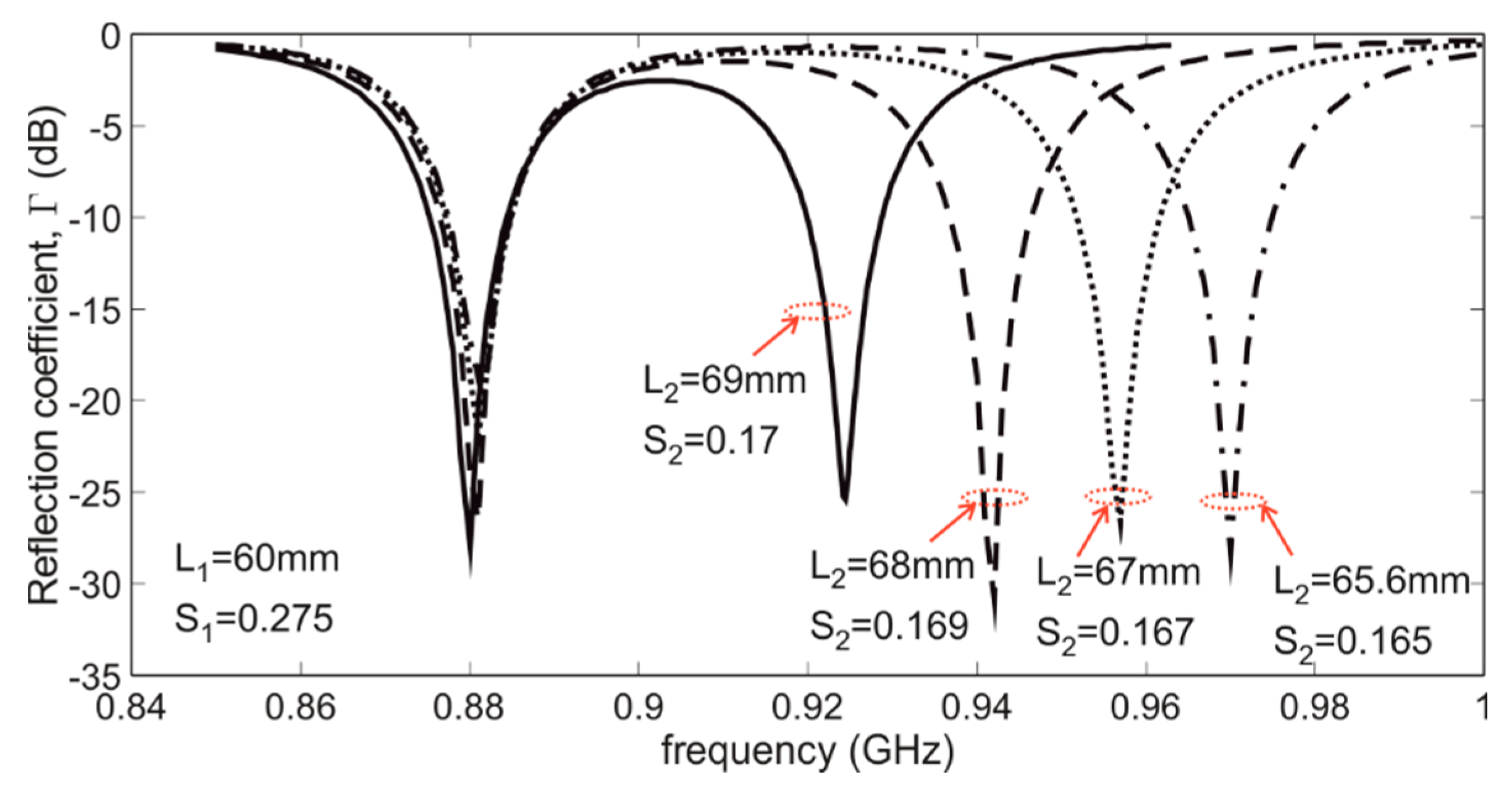
In conclusion, the proposed fractal MA-cell offers reduced thickness (≅λ/100) and small unit cells (≅0.4λ) at both operating frequencies, with respect to the most existing dual-band MA configurations (see Table 1). Moreover, it allows to achieve very close absorbing peaks by virtue of combining two distinct pairs of resonators both characterized by two degrees of freedom (i.e., the fractal sizes (Li, Si) −i = 1, 2, see Figure 1). In fact, the latter can be specifically tuned to obtain very close resonance lengths (i.e., = (1 + 2Si) Li, i = 1, 2, see Figure 1), namely very close resonant frequencies (fi ~ 1/), assuring at the same time perfect absorption at both resonant frequencies. A quick demonstration of the above statements is reported in Figure 5, showing the design of a MA cell with closer absorption peaks. In particular, the 1st absorption frequency is fixed to the value f1 = 880 MHz, while the 2nd absorption frequency is shifted down from 970 MHz to 925 MHz, by changing both parameters L2 and S2 in order to increase the effective length , thus guaranteeing at the same time a well matched impendence, namely a good absorptivity (i.e., Γ(f2) ≤ −25 dB ⇒ A(f2) ≥ −99.6%).
3. Experimental Validation
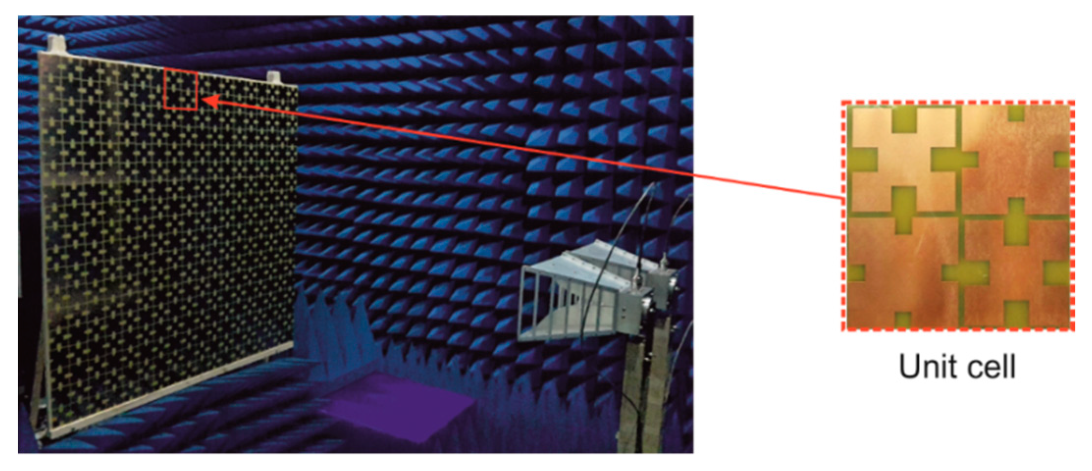
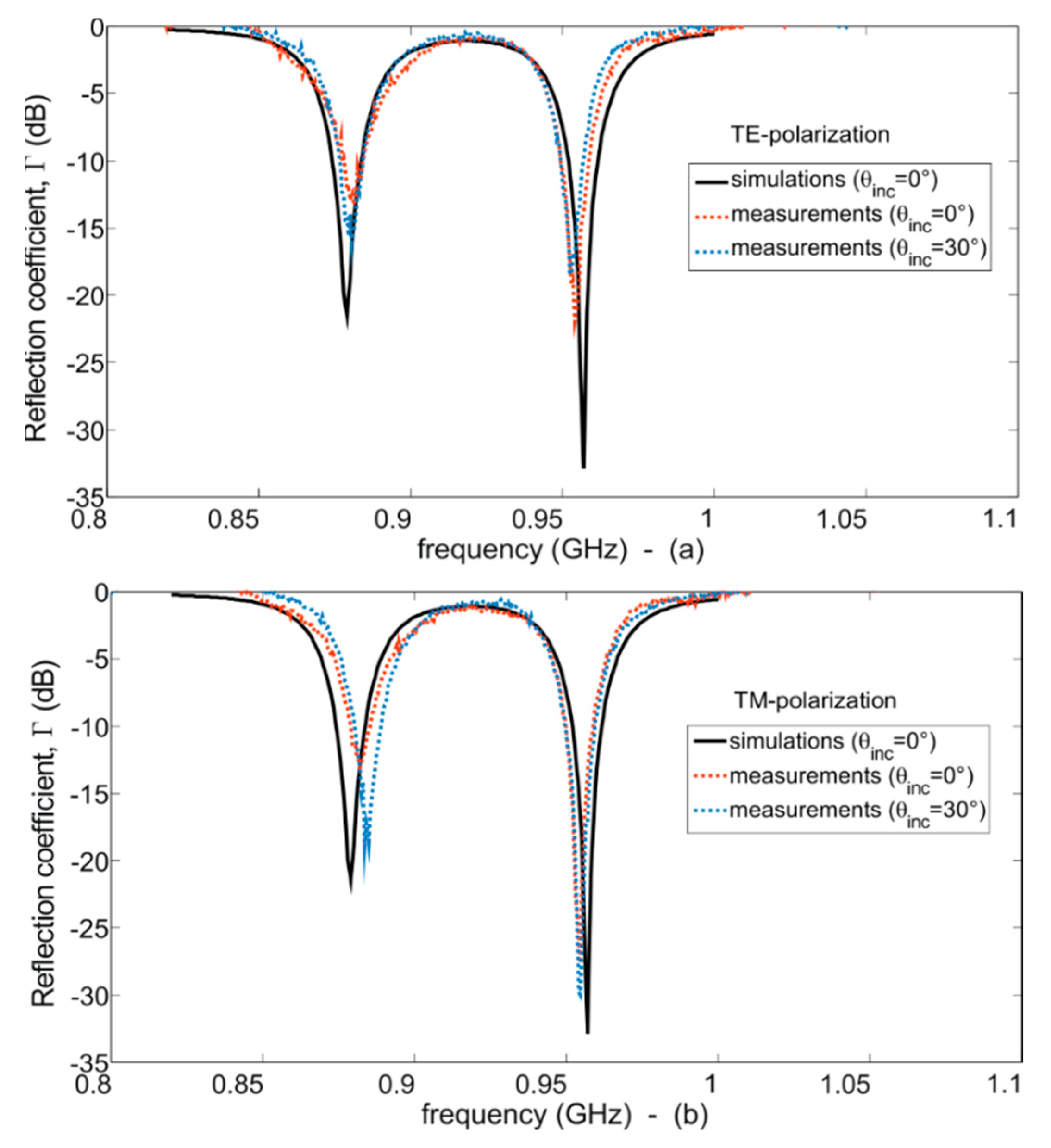
To perform a preliminary experimental validation of the proposed dual-band configuration, a 125 mm × 125 mm absorber panel, composed by 18 × 18 fractal elements, is realized and tested in the anechoic chamber of the Microwave Laboratory of the University of Calabria, which is equipped for both near-field and far-field measurements [21,22]. For the specific application, a far-field experimental setup (Figure 6), including a transmitting and a receiving broadband horn antennas, is adopted to measure the reflection coefficient of the absorbing panel. Both horn antennas, connected to a vector network analyzer (VNA), are placed at a distance X from the panel satisfying the far-field condition (i.e., X > 2D2/λ0, where D is the diagonal length of the horn antennas). The horns are rotated on their own axis in order to measure the panel reflection coefficient, for incident signals in both TE and TM polarization. The reflection coefficient of the MA panel (Figure 7) is measured under normal incidence (i.e., θinc ≅ 0°). An absorptivity greater than 96% and 99.4% is demonstrated at the frequencies f1 and f2, respectively, for both polarizations (Figure 7). Furthermore, a very good agreement is achieved between experimental and simulation data (Figure 7), thus demonstrating the effectiveness of the proposed dual-band fractal MA to realize perfect absorption. Finally, very low sensitivity to the angular variation of the incident wave is experimentally checked for both TE and TM polarizations (Figure 7).
4. Conclusions
The compactness capabilities of fractal geometries have been considered in this paper to design a dual-band microwave absorber operating within the UHF band. Very high absorption peaks (>99%) have been simulated in the neighborhood of the desired working frequencies (i.e., 878 MHz and 956 MHz). A fractal MA panel has been prototyped and experimentally validated, confirming the capabilities of the proposed configuration in realizing the perfect absorption condition under the dual-frequency modality, thus saving thickness and size as compared to standard microwave absorbing configurations.
Author Contributions
The individual contributions of authors are specified as follows: Conceptualization, S.C. and F.V.; methodology, S.C. and F.V.; software, F.V.; validation, S.C., F.V., and A.B.; writing—original draft preparation, F.V. and A.B.; writing—review and editing, S.C.; supervision, S.C.
Funding
This research received no external funding.
Conflicts of Interest
The authors declare no conflict of interest.
References
- Munk, B.A. Frequency Selective Surfaces: Theory and Design; Wiley Interscience: New York, NY, USA, 2000. [Google Scholar]
- Landy, N.I.; Sajuyigbe, S.; Mock, J.J.; Smith, D.R.; Padilla, W.J. Perfect metamaterial absorber. Phys. Rev. Lett. 2008, 100, 207402. [Google Scholar] [CrossRef] [PubMed]
- Watts, C.M.; Liu, X.; Padilla, W.J. Metamaterial electromagnetic wave absorbers. Adv. Mater. 2012, 24, 98–120. [Google Scholar] [CrossRef] [PubMed]
- Okano, Y.; Ogino, S.; Ishikawa, K. Development of optically transparent ultrathin microwave absorber for ultrahigh-frequency RF identification system. IEEE Trans. Microw. Theory Tech. 2012, 60, 2456–2464. [Google Scholar] [CrossRef]
- Costa, F.; Genovesi, S.; Monorchio, A.; Manara, G. Low-cost metamaterial absorbers for sub-GHz wireless systems. IEEE Antennas Wirel. Propag. Lett. 2014, 13, 27–30. [Google Scholar] [CrossRef]
- Costa, F.; Genovesi, S.; Monorchio, A.; Manara, G. Perfect metamaterial absorbers in the ultra-high frequency range. In Proceedings of the International Symposium on Electromagnetic Theory, Hiroshima, Japan, 20–24 May 2013. [Google Scholar]
- Zuo, W.; Yang, Y.; He, X.; Zhan, D.; Zhang, Q. A miniaturized metamaterial absorber for ultrahigh-frequency RFID system. IEEE Antennas Wirel. Propag. Lett. 2017, 16, 329–332. [Google Scholar] [CrossRef]
- Venneri, F.; Costanzo, S.; Di Massa, G. Fractal-shaped metamaterial absorbers for multireflections mitigation in the UHF band. IEEE Antennas Wirel. Propag. Lett. 2018, 17, 255–258. [Google Scholar] [CrossRef]
- Venneri, F.; Costanzo, S.; Di Massa, G. Multi-band designs of fractal microwave absorbers. In Advances in Intelligent Systems and Computing, Proceedings of the WorldCIST’18, Naples, Italy, 27–29 March 2018; Springer: Cham, Switzerland, 2018; Volume 746. [Google Scholar]
- Singh, D.; Srivastava, V.M. Dual resonance shorted stub circular rings metamaterial absorber. Int. J. Electron. Commun. (AEÜ) 2018, 83, 58–66. [Google Scholar] [CrossRef]
- Li, M.H.; Yang, H.L.; Hou, X.W. Perfect metamaterial absorber with dual bands. PIER 2010, 108, 37–49. [Google Scholar] [CrossRef]
- Jamilan, S.; Azarmanesh, M.N.; Zarifi, D. Design and characterization of a dual-band metamaterial absorber based on destructive interferences. PIER C 2014, 47, 95–101. [Google Scholar] [CrossRef]
- Dincer, F.; Karaaslan, M.; Unal, E.; Delihacioglu, K.; Sabah, C. Design of polarization and incident angle insensitive dual-band metamaterial absorber based on isotropic resonator. PIER 2014, 144, 123–132. [Google Scholar] [CrossRef]
- Park, J.W.; Tuong, P.V.; Rhee, J.Y.; Kim, K.W.; Jang, W.H.; Choi, E.H.; Chen, L.Y.; Lee, Y.P. Multi-band metamaterial absorber based on the arrangement of donut-type resonators. Opt. Express 2013, 21, 9691–9702. [Google Scholar] [CrossRef] [PubMed]
- Shen, X.; Cui, T.J.; Zhao, J.; Ma, H.F.; Jiang, W.X.; Li, H. Polarization-independent wide-angle triple-band metamaterial absorber. Opt. Express 2011, 19, 9401–9407. [Google Scholar] [CrossRef] [PubMed]
- Mishra, N.; Choudhary, D.K.; Chowdhury, R.; Kumari, K.; Chaudhary, R.K. An investigation on compact ultra-thin triple band polarization independent metamaterial absorber for microwave frequency applications. IEEE Access 2017, 5, 4370–4376. [Google Scholar] [CrossRef]
- Huang, L.; Chen, H. Multi-band and polarization insensitive metamaterial absorber. PIER 2011, 113, 103–110. [Google Scholar] [CrossRef]
- Costanzo, S.; Venneri, F. Miniaturized fractal reflectarray element using fixed-size patch. IEEE Antennas Wirel. Propag. Lett. 2014, 13, 1437–1440. [Google Scholar] [CrossRef]
- Costanzo, S.; Venneri, F.; Di Massa, G.; Borgia, A.; Costanzo, A.; Raffo, A. Fractal reflectarray antennas: State of art and new opportunities. Int. J. Antennas Propag. 2016, 2016, 17. [Google Scholar] [CrossRef]
- Costa, F.; Genovesi, S.; Monorchio, A.; Manara, G. A circuit-based model for the interpretation of perfect metamaterial absorbers. IEEE Trans. Antennas Propag. 2013, 61, 1201–1209. [Google Scholar] [CrossRef]
- Costanzo, S.; Di Massa, G. An integrated probe for phaseless near-field measurements. Measurement 2002, 31, 123–129. [Google Scholar] [CrossRef]
- Costanzo, S.; Di Massa, G. Direct far-field computation from bi-polar near-field samples. J. Electromagn. Waves Appl. 2006, 20, 1137–1148. [Google Scholar] [CrossRef]
Figure 1.
Fractal metamaterial absorber: dual-band unit cell.

Figure 2.
Reflection coefficient and unit cell input impedance vs. frequency for different cell sizes D: (a) fractal-based cell; (b) square-based cell.
Figure 2.
Reflection coefficient and unit cell input impedance vs. frequency for different cell sizes D: (a) fractal-based cell; (b) square-based cell.

Figure 3.
Current on the patch surface @ 868 MHz (D = 0.2λ – L = 60.9 mm, S = 0.257).

Figure 4.
Reflection coefficient vs. frequency of the synthesized dual-band metamaterial absorber (MA) cell for different incidence angles (εr = 4.2, tanδ = 0.015 and h = 3.2 mm–D ≅ 0.4λ @ f1): (a) TE-polarization (b) TM-polarization.
Figure 4.
Reflection coefficient vs. frequency of the synthesized dual-band metamaterial absorber (MA) cell for different incidence angles (εr = 4.2, tanδ = 0.015 and h = 3.2 mm–D ≅ 0.4λ @ f1): (a) TE-polarization (b) TM-polarization.

Figure 5.
Reflection coefficient vs. frequency of a synthesized dual-band MA for different (L2, S2)-values (εr = 4.2, tanδ = 0.015 and h = 3.2 mm–D ≅ 0.4λ @ f1).
Figure 5.
Reflection coefficient vs. frequency of a synthesized dual-band MA for different (L2, S2)-values (εr = 4.2, tanδ = 0.015 and h = 3.2 mm–D ≅ 0.4λ @ f1).

Figure 6.
Free-space measurement setup with a particular of the fabricated MA absorber.

Figure 7.
Comparison between measured and simulated reflection coefficients vs. frequency: (a) TE-polarization; (b) TM-polarization.
Figure 7.
Comparison between measured and simulated reflection coefficients vs. frequency: (a) TE-polarization; (b) TM-polarization.


Table 1.
Comparison with previously proposed dual-band MAs.
| Configuration | f1 (GHz) | f2 (GHz) | Cell Periodicity | Thickness |
|---|---|---|---|---|
| Present work | 0.878 | 0.956 | ≅0.4λ1 (0.44λ2) | λ1/107 (λ2/98) |
| [10] | 17 | 18 | ≅0.5λ1 (0.54λ2) | λ1/44 (λ2/42) |
| [11] | 11.15 | 16 | ≅0.45λ1 (0.64λ2) | λ1/54 (λ2/38) |
| [12] | 5.6 | 6 | ≅0.38λ1 (0.4λ2) | λ1/36 (λ2/33) |
| [13] | 4.42 | 5.62 | ≅0.44λ1 (0.56λ2) | λ1/42 (λ2/33) |
© 2019 by the authors. Licensee MDPI, Basel, Switzerland. This article is an open access article distributed under the terms and conditions of the Creative Commons Attribution (CC BY) license (http://creativecommons.org/licenses/by/4.0/).
Share and Cite
MDPI and ACS Style
Venneri, F.; Costanzo, S.; Borgia, A. A Dual-Band Compact Metamaterial Absorber with Fractal Geometry. Electronics 2019, 8, 879. https://0-doi-org.brum.beds.ac.uk/10.3390/electronics8080879
AMA Style
Venneri F, Costanzo S, Borgia A. A Dual-Band Compact Metamaterial Absorber with Fractal Geometry. Electronics. 2019; 8(8):879. https://0-doi-org.brum.beds.ac.uk/10.3390/electronics8080879
Chicago/Turabian StyleVenneri, Francesca, Sandra Costanzo, and Antonio Borgia. 2019. "A Dual-Band Compact Metamaterial Absorber with Fractal Geometry" Electronics 8, no. 8: 879. https://0-doi-org.brum.beds.ac.uk/10.3390/electronics8080879
Note that from the first issue of 2016, this journal uses article numbers instead of page numbers. See further details here.