1. Introduction
With the continued aggressive scaling of CMOS technologies, the speed of digital circuits has been increasing and their power consumption decreasing. These benefits, however, come at the cost of decreased intrinsic device gain, thereby hurting the performance of analog circuits [
1]. On the other hand, high-precision applications require operational transconductance amplifiers (OTAs) with high DC gain. The traditional solution for this problem has been to stack transistors vertically in a cascode configuration so as to achieve a high DC gain with a nearly first-order response.
As scaling continues, however, supply voltages also need to be scaled down to ensure device reliability. This results in reduced signal headroom and renders conventional cascode techniques unreliable [
2,
3]. For this reason, modern OTAs tend to involve a cascade of multiple stages (three or more) to achieve the desired gain.
Even though some authors have demonstrated the successful design of four-stage OTAs [
4,
5,
6] and some have gone beyond that to describe
n-stage OTAs [
7,
8,
9], three-stage OTAs remain a reasonable tradeoff between complexity and power efficiency and have therefore garnered a lot of research interest for diverse applications over the past 20 years or more.
Applications for three-stage OTAs include headphone amplifiers, liquid crystal display (LCD) drivers, low-dropout (LDO) linear regulators and capacitive MEMS sensors [
3,
10,
11,
12,
13]. Some applications (for example, MEMS and active matrix LCD) require the amplifier to drive very large capacitive loads [
14] and others (e.g., headphone drivers and MEMS sensors) need the amplifier to be able to drive a wide range of load capacitors over several orders of magnitude [
3,
15].
The main challenge in three-stage OTA design is the compensation of the resulting three-pole system. The compensation architectures that have been devised to address this issue tend to be complicated and defy a tractable intuitive analysis and several works have been dedicated to deriving intuitive expressions for three-stage OTA transfer functions once their compensation structure is given [
16,
17,
18,
19,
20]. These works allow engineers to quickly derive expressions for pole and zero frequencies to be used in hand analysis and design but do not comment on the relative merits of different compensation architectures.
Moreover, this challenging and extended design space has led to a proliferation of solutions and approaches to the compensation problem, with Miller compensation being chief among them. Classical architectures relied on nested Miller compensation [
2,
7,
21,
22,
23,
24,
25,
26,
27] and it remains an attractive solution today [
12,
28]. Architectures that rely on reverse nested Miller provide an improved power efficiency [
3,
13,
29,
30,
31,
32,
33] but it has been recognized that nesting Miller capacitors leads to bulky and slow implementations and many architectures were devised to use a single Miller capacitor along with some ancillary compensation structures [
4,
11,
14,
34,
35,
36,
37,
38,
39,
40,
41,
42,
43,
44,
45,
46,
47,
48]. Some authors have also demonstrated compensation techniques that do not rely on a Miller capacitor at all [
8,
49,
50,
51,
52].
With the plethora of existing architectures, the task of choosing a compensation technique for a given application becomes daunting and a review of available solutions is much needed. To this end, many reviews and tutorials have been published to compare existing compensation architectures [
53,
54,
55], analyze their distortion and noise performance [
56,
57,
58] and optimize their settling time performance [
59,
60,
61,
62,
63].
Most of these tutorials and reviews focus on a specific application or a specific type of compensation architecture and very few of them provide the means to compare different compensation architectures prior to having designed them at the transistor-level. In this review article, a large selection of three-stage OTA compensation architectures are reviewed and compared. Furthermore, a novel figure of merit is proposed, allowing a priori comparison of the power efficiency of different compensation architectures. This figure of merit exposes the tradeoffs involved in each compensation technique and can be used as a guide to architecture selection once an analytical expression for the OTA’s transfer function is obtained.
In addition to fine-grained architecture comparison, a taxonomic classification of the extant compensation architectures is proposed. This taxonomy divides the different compensation architectures into three broad categories and extracts the common features of the architectures in each one of them. It can therefore be used to steer the design focus towards compensation architectures that are more suitable to the application at hand and even predict qualitative properties of new OTA architectures according to where they fall in the taxonomy. To the authors’ best knowledge, this is the first time such a classification scheme has been proposed.
The rest of this paper is organized as follows:
Section 2 starts by examining control-theoretic issues common to all three-stage OTAs where it is noted that the current approach of designing the amplifier for a target phase margin [
3,
33,
43,
44,
45,
46,
48] without regard to other stability metrics can lead to a design that performs sub-optimally [
62,
64] and is wasteful of power. With the common challenges noted and the design procedure of optimizing the response for settling time instead is outlined, the proposed figure of merit for architecture comparison is explained in detail.
Section 3 describes the proposed OTA classification scheme and describes the common features and the suitable applications for each category.
Section 4 discusses circuit-level considerations that arise during the implementation of three-stage OTAs. In
Section 5, transistor-level simulations of selected architectures at a fixed power budget help confirm the discussion and make it more concrete. Conclusions are given in
Section 6.
2. A Control Perspective on Multistage Amplifier Design
Compared to a two-stage OTA, ensuring the stability of a three-stage OTA is more complicated since the added high-impedance node introduces an additional low-frequency pole to the transfer function.
As the transfer function order increases, several challenging issues arise in the design. This section highlights these issues and outlines an alternate design procedure to overcome them. Once the general design procedure is outlined, a method for comparing architectures and selecting a suitable one for a given application is proposed, so that the design procedure can be applied to a specific architecture.
2.1. Challenges in Multistage Amplifier Compensation
The first main design challenge is that the phase margin, used extensively as a stability metric in the design of two-stage OTAs, is no longer an adequate indicator of stability by itself. Furthermore, it is quite difficult to derive accurate phase and gain margin formulas to be used for hand analysis and design. These issues are explored in detail in the following subsections.
2.1.1. Inadequacy of the Phase Margin as a Stability Criterion
Consider a simplified three-stage OTA with a dominant pole, a pair of non-dominant poles and no zeros. The open-loop gain of such an OTA may be expressed as
where
is the DC gain,
is the dominant pole frequency and
and
Q represent the natural frequency and quality factor of the non-dominant pole pair, respectively.
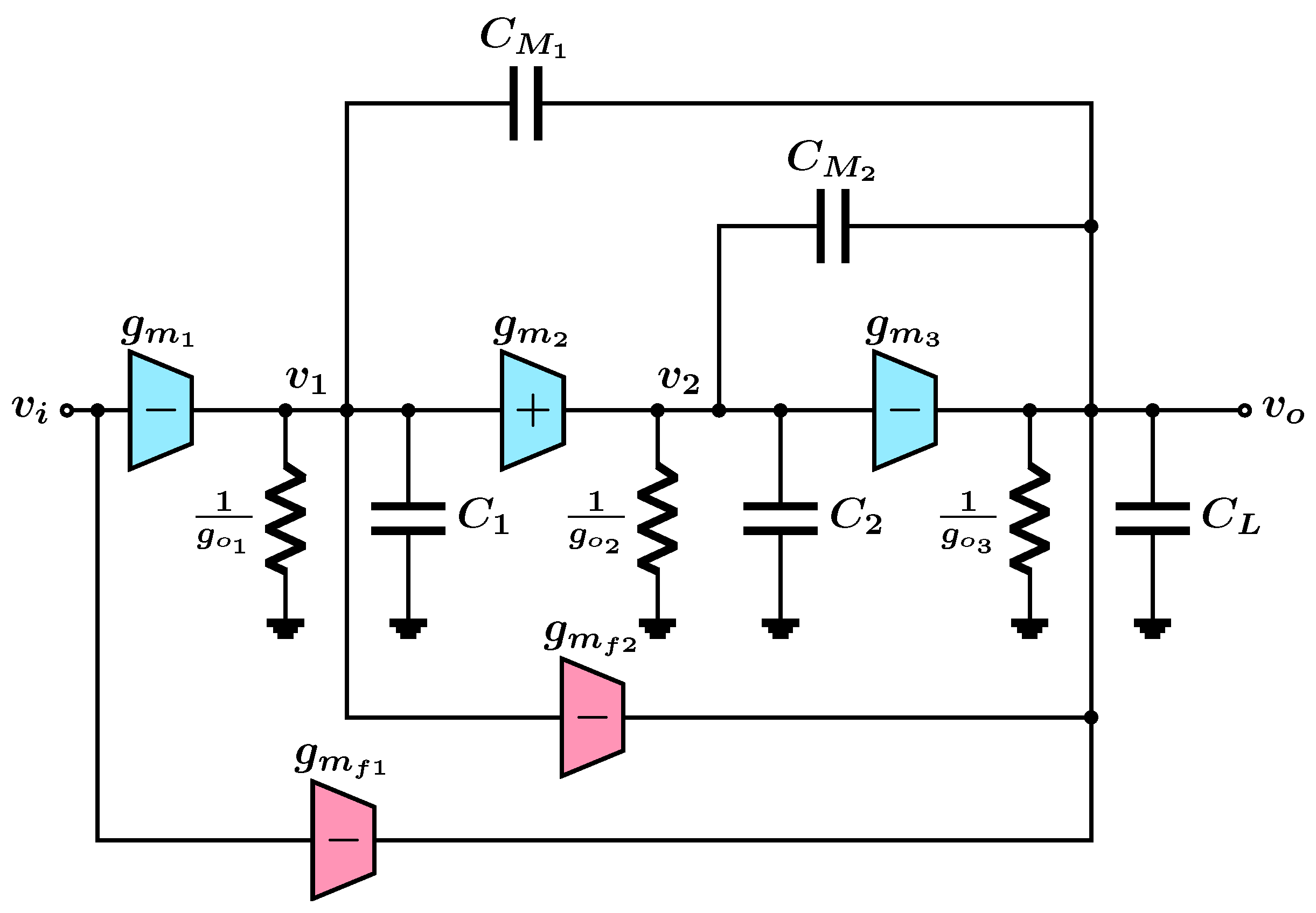
As an example implementation, consider the small-signal block diagram shown in
Figure 1 which represents a nested
-C compensation architecture [
7].
and
represent the output conductance and parasitic capacitance of stage
i, respectively, while
represents the load capacitance. With
and
, the open-loop transfer function of this OTA has the same form as Equation (
1). Using the notation of
Figure 1, the parameters of this OTA’s transfer function are shown in
Table 1.
Under unity-gain feedback, the closed-loop transfer function of this OTA becomes
Applying the Routh–Hurwitz stability criterion [
65] to this function yields the following stability condition
Under the assumptions
,
and
, this can be simplified to
with
, the normalized non-dominant pole frequency, defined as
where GBW stands for the gain-bandwidth product. With reference to the example of
Figure 1 and
Table 1, one gets
so, for a specified GBW, the parameter
correlates with power consumption through the transconductances
and
. This is true for other three-stage OTAs as well since
relates to how far the non-dominant poles are pushed beyond the GBW.
Denoting the unity-gain frequency (UGF) by
, the phase margin may be expressed with reference to Equation (
1) as
Moreover, approximating the UGF using GBW (
) (this assumes, as expressed in Equation (
1), a single dominant pole and therefore a 20 dB/decade magnitude roll-off from
to the UGF), the phase margin may be approximated as
Contours for the approximate phase margin function in Equation (
7) are plotted in the
space in
Figure 2. The figure shows clearly that, even when the phase margin is as high as 80°, some designs can violate the Routh–Hurwitz criterion and end up in the unstable region because they have negative gain margin, as demonstrated below. This means that there will be more than one UGF leading to the formula in Equation (
7) no longer being valid.
Since there is an infinite number of ways to achieve a given phase margin, the inset plot compares the unity-gain feedback responses for two different designs that both have a phase margin of 60° usually deemed enough for most designs. The red plot corresponds roughly to the approach of requiring the closed loop poles to correspond to those of a third-order Butterworth filter (see, for example, [
22,
25]) while the blue plot corresponds to setting
.
The plots demonstrate the superiority of the Butterworth pole spacing approach while also highlighting the inadequacy of relying on the phase margin as the sole measure of stability with no consideration given to other metrics such as the gain margin or the Routh–Hurwitz criterion. The situation, of course, gets more complicated when the OTA has zeros and/or additional parasitic poles close to its UGF as in more complicated compensation architectures.
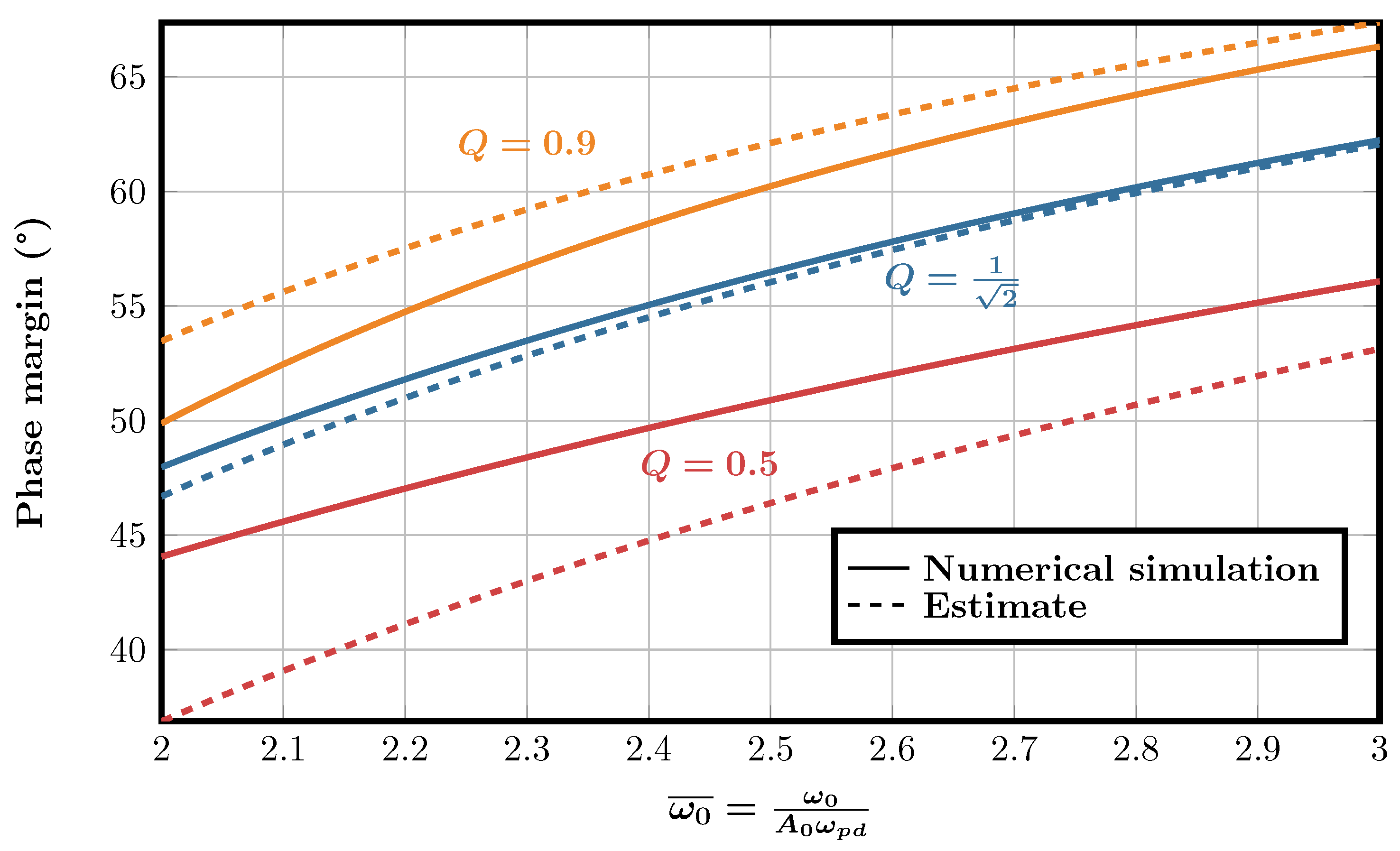
2.1.2. Difficulty of Estimating the Gain and Phase Margins
Another challenge in the design of three-stage OTAs lies in the difficulty of estimating the gain and phase margins accurately.
In the simplified case of three poles and no zeros, estimating the gain margin is relatively simple as shown below but in the general case, when the OTA has zeros and/or additional parasitic poles, estimating the gain margin accurately through hand analysis is quite difficult if not outright impossible.
In addition, estimating the phase margin accurately, even in the simple case of the OTA given by Equation (
1), is quite tricky because finding the gain crossover frequency requires solving the sixth-order equation
This equation can be shown to reduce to the commonly-used estimate
when
and
. When these conditions are not fulfilled, however, approximating the gain crossover frequency using the gain-bandwidth product is not accurate. This can be seen in
Figure 3 where the phase margin of the same OTA is plotted as a function of
for several values of
Q. Along with the results of numerical simulations using Equation (
8), the dashed plots show the phase margin estimated from the approximate formula (see
Appendix A):
along with
. As the figure shows, the estimate is quite good for
(which is the value used in the Butterworth pole spacing approach) but can be quite inaccurate for other values of
Q and its accuracy gets worse as
is decreased in order to save power. In the worst case, the required
(and therefore power) to achieve a phase margin of 45° is overestimated by 17% when using the analytical formula, leading to an over-designed solution.
2.1.3. Alternative Design Approach
The conventional approach used in recent designs that target wide load range applications [
3,
33,
43,
44,
45,
46,
48] is to design the amplifier to meet a minimum phase margin specification at the maximum desired load capacitance. However, as argued above and recognized in [
62], targeting a specific phase margin is not necessarily the optimal strategy for achieving a fast settling response. Furthermore, as shown below, the same phase margin may be achieved with quite different power budgets. Therefore, a good design procedure should focus on settling response parameters from the start.
The alternative approach suggested here is to focus on the time-domain settling behavior and optimize the settling time as has been suggested in [
59] and the overshoot as a function of amplifier parameters.
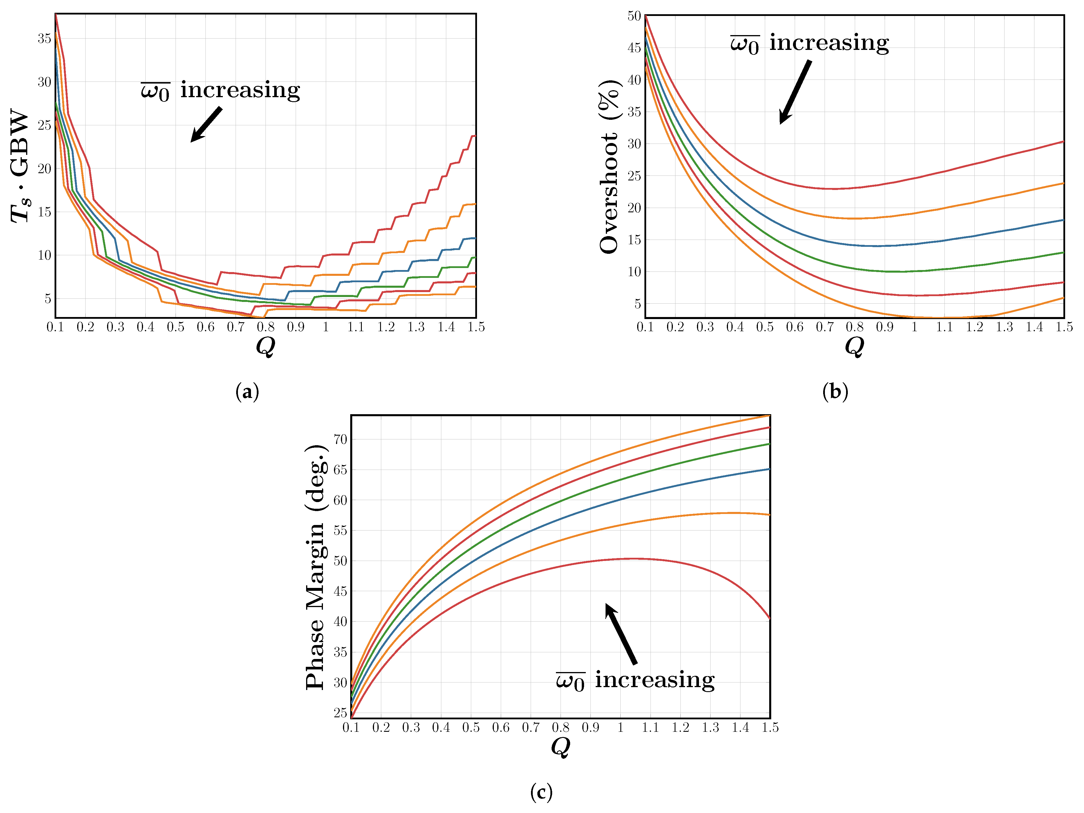
As an example to further reinforce the point,
Figure 4 shows the phase margin and the normalized settling time (
) and/or overshoot percentage for the unity-gain feedback step response of the OTA given by Equation (
1). These quantities are plotted as functions of
Q for different values of
. As the figures show, maximizing the phase margin does not correspond to minimizing the time-domain settling parameters. Note from the figure that, even though phase margin is not a sufficient indicator of settling performance, values of
where the maximum achievable phase margin is low have large values for the minimum possible settling time and overshoot, so that phase margin puts a lower limit on the best achievable settling performance [
62].
To compare the results of different design approaches, the performance of four different solutions is compared. The parameters of the different designs are shown in
Table 2 along with the rationale used in selecting them.
With reference to
Table 1, the power requirements for an NGCC OTA to achieve certain
and
Q values can be estimated. In particular, the transconductance of the last stage can be estimated as
which can then be used to compare the designs.
The foru design cases in
Table 2 were numerically simulated, assuming a GBW of
, and their performance is summarized in
Table 3 along with the calculated value of
required to drive a 100 pF load with the above-mentioned GBW. The table illustrates that designing the OTA for a specified phase margin can lead to a significant power dissipation (Case 1) that is more than 3× that of the design that obtains a similar performance with a focus on minimizing settling time at a given power consumption (Case 2). Furthermore, at nearly the same power expenditure, the settling time can be improved by 47.2% when the main goal is to minimize overshoot and settling time (Case 3). Finally, it is shown that this approach achieves a similar performance to the Butterworth pole spacing approach (Case 4) at 25% less power consumption.
Thus, from a performance perspective, once a compensation architecture is selected, macro-model simulations should be used to generate curves similar to
Figure 4 for the selected architecture and select the OTA parameters based on the specified time-domain performance parameters at maximum load capacitance. The issue of selecting a compensation architecture is tackled next.
2.2. Architecture Selection
The addition of an extra gain stage and other compensation structures means that the design space of the OTA is quite larger than that for a two-stage OTA, and there are many more possible architectures and compensation strategies for a multi-stage OTA [
2,
8,
31,
36,
37,
49]. This abundance of architectures can be confusing for designers searching for an OTA architecture suitable for a given application.
For comparing different architectures, several different figures-of-merit (FoM) have been proposed. The most famous set of FoMs is (see, for example [
27,
38,
48]):
where GBW, SR,
and
denote the gain-bandwidth product, the slew rate, the load capacitance and the supply current, respectively. These FoMs are widely used because they capture both the small- and large-signal settling behavior of the OTA while also favoring OTAs that are capable of driving large capacitive loads.
However, the above FoMs do not account for the area efficiency of the OTA; in particular, no mention of the total size of the required on-chip compensation capacitance is given. For this reason, the authors of [
28] introduced FoMs for large-capacitive-load OTAs:
where
is the total compensation capacitance.
These FoMs give a better picture of area efficiency but become irrelevant (in the sense that they become infinite) for OTAs that do not rely on any compensation capacitors such as those in [
8,
49,
50,
51], which have to rely on the old FoMs in this case.
In addition, none of the above FoMs gives an indication of how complicated the compensation strategy for each architecture is: they are all performance-oriented and are calculated based on experimental results. In that sense, the same OTA architecture can have different FoM values depending on how its design was approached. These FoMs therefore do not allow for an a priori comparison between different architectures for a particular application.
At least two FoMs have been proposed that quantify the power efficiency of the compensation strategy of an OTA. The first one is the transconductance efficiency factor defined in [
37] as a ratio of the OTA’s GBW to the GBW of the single stage amplifier composed of the OTA’s last stage:
where
is the transconductance of the last stage. The authors of [
37] related the transconductance of the last stage to the GBW by imposing the Butterworth condition on the unity-gain feedback OTA while neglecting any zeros in the open-loop response. As such, the transconductance efficiency is valid for comparing different kinds of OTAs, including ones that do not employ any compensation capacitors but fail to capture the effects of open-loop zeros on the compensation strategy.
The second FoM, as suggested by the authors of [
54], can be analytically evaluated in order to facilitate the comparison of compensation architectures:
where
is the sum of all transconductance values in the amplifier that require a dedicated bias current. The authors demonstrated that this FoM can be used to compare different compensation architectures analytically but again, the approach taken by the authors neglects the effects of zeros.
Finally, the authors of [
59] derived a FoM that can be used to compare amplifiers with optimized settling time:
where
is the required settling accuracy in the time domain and
is the minimum achievable settling time of the amplifier to an accuracy of
. This FoM is very useful for comparing architectures based on their achievable time domain performance but cannot be derived analytically since
has no known closed-form solution.
For these reasons, the next section proposes a new FoM that allows for the comparison of different OTA architectures based on the power efficiency of their compensation schemes.
2.3. Proposed FoM for Architecture Selection
The Routh–Hurwitz stability criterion for a third-order polynomial is . When , this indicates a pole that is about to cross into the right half-plane (RHP) and thus indicates the marginal stability of the system being studied. Since the roots of a polynomial depend in a continuous manner on its coefficients, it is reasonable to expect that as the quantity increases, the roots of the polynomial move further into the left half-plane (LHP) rendering the system “more stable” in some sense.
Based on the above discussion, the proposed FoM for compensation efficiency is obtained by considering the OTA in unity-gain feedback without neglecting its zeros as has been done in [
22,
25,
37]. With the coefficients
representing the closed-loop pole polynomial thus formed, the proposed FoM is defined as
To give an indication of how useful this FoM can be we return to the all-pole OTA whose open-loop gain is given by Equation (
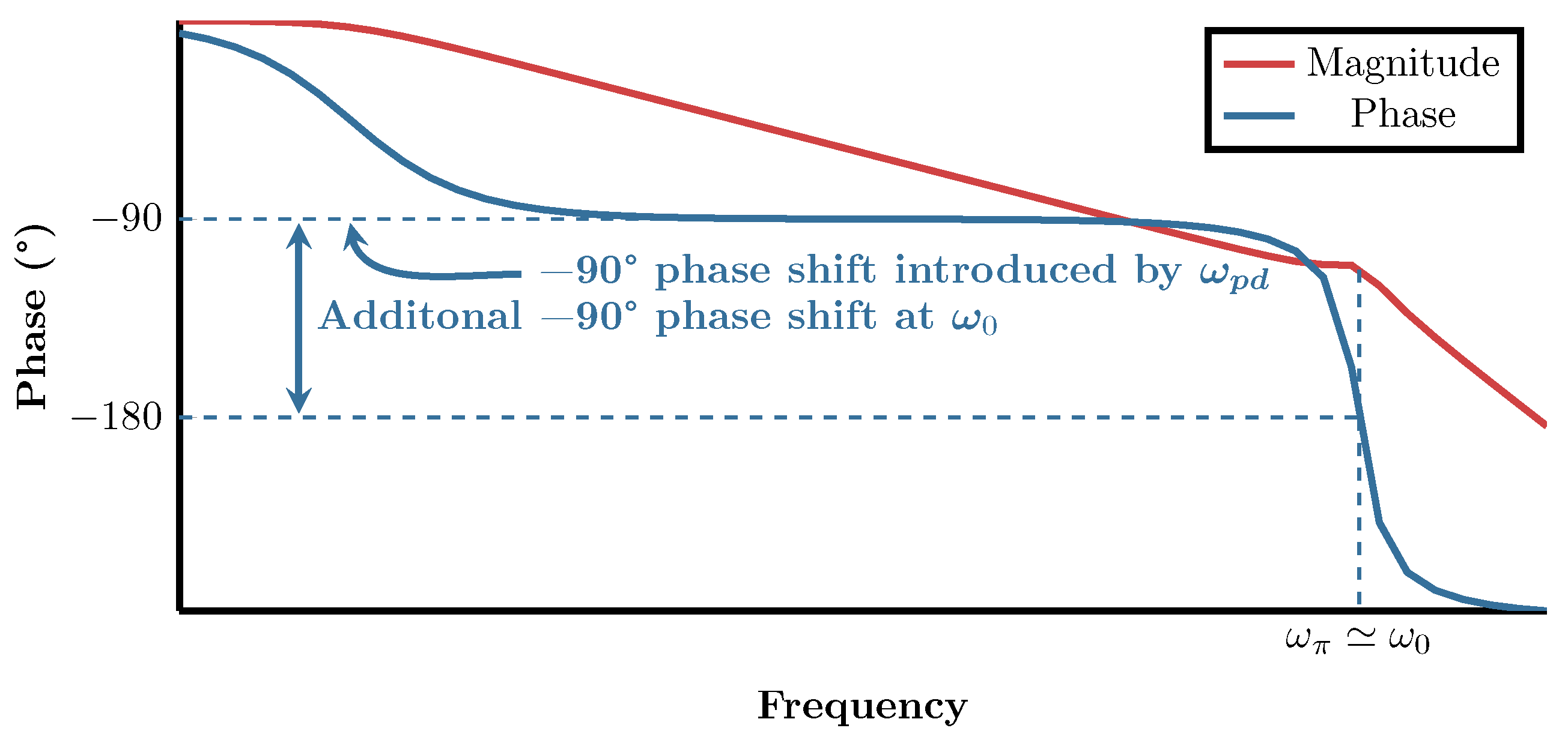
1). If we consider the Bode plot of the open-loop gain, sketched conceptually in
Figure 5, we note that the complex pole pair contributes −90° of phase shift at
. It is thus reasonable to estimate the phase crossover frequency as
since the dominant pole also contributes −90° of phase shift at
(where it is assumed that
). It can thus be shown that in this case, the gain margin is given by
Thus, according to Equation (
4),
corresponds exactly to the gain margin in this case so that a higher
corresponds to a higher gain margin for this OTA.
The factor
can be used as a measure of how power-efficient a compensation scheme is. In particular, higher values of
mean that, for the same increase in power consumption, the improvement in stability is larger. This can be demonstrated by observing the effects of doubling the value of
(doubling the power consumption) at two different values of
.
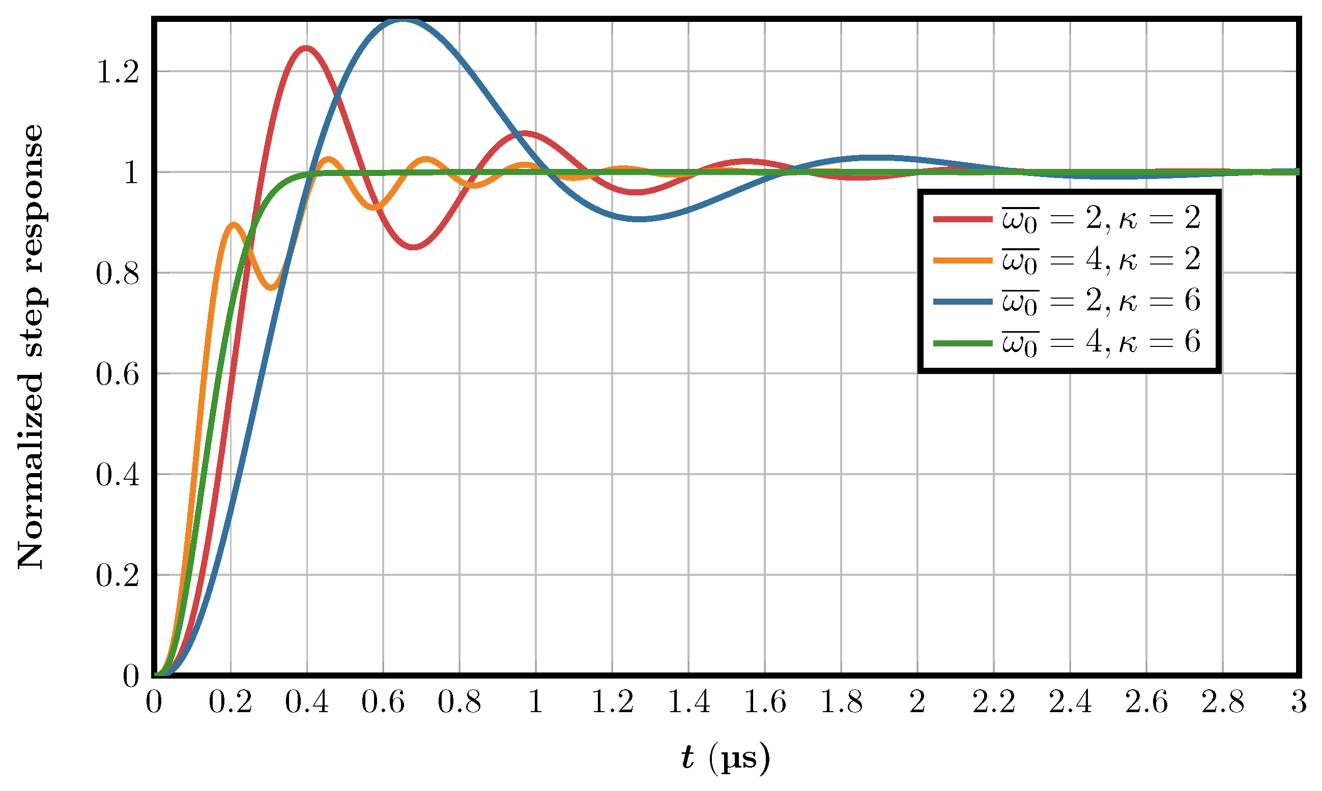
Figure 6 demonstrates the unity-gain feedback step response in four cases:
is doubled from 2 to 4 at
and
and
Table 4 summarizes the settling time in each case as well as the improvement obtained from doubling the power consumption. The results demonstrate that an increased power consumption achieves a better stability improvement for larger values of
.
This FoM can also be used for comparing two different compensation architectures. To demonstrate this, consider another three-stage OTA with a zero in the LHP such that its open-loop gain is given by
In this case, the closed-loop pole polynomial coefficients, assuming unity-gain feedback, are given by
so that
is given by
This result is quite intuitively satisfying since it shows that this new OTA has a higher
than the one given by Equation (
1) and that this improvement is due to the LHP zero. Moreover, it can be seen that this improvement becomes insignificant when the zero frequency is much larger than the GBW product of the OTA.
The main limitation of using
as a FoM is that it cannot deal with pole-zero cancellations. This is not a very serious limitation, however, since OTAs that rely on pole-zero cancellation usually achieve this cancellation at a specific value of the load capacitor. Any change in the load capacitor makes the OTA return to being a three-pole system and justifies the use of
[
64].
It should also be noted that OTAs having more than three poles due to additional parasitic poles have a different Routh–Hurwitz stability condition to the one derived here. This is ignored in our work on the basis that the parasitic poles are at such high frequencies that they do not significantly affect the OTA’s stability [
33,
38,
48].
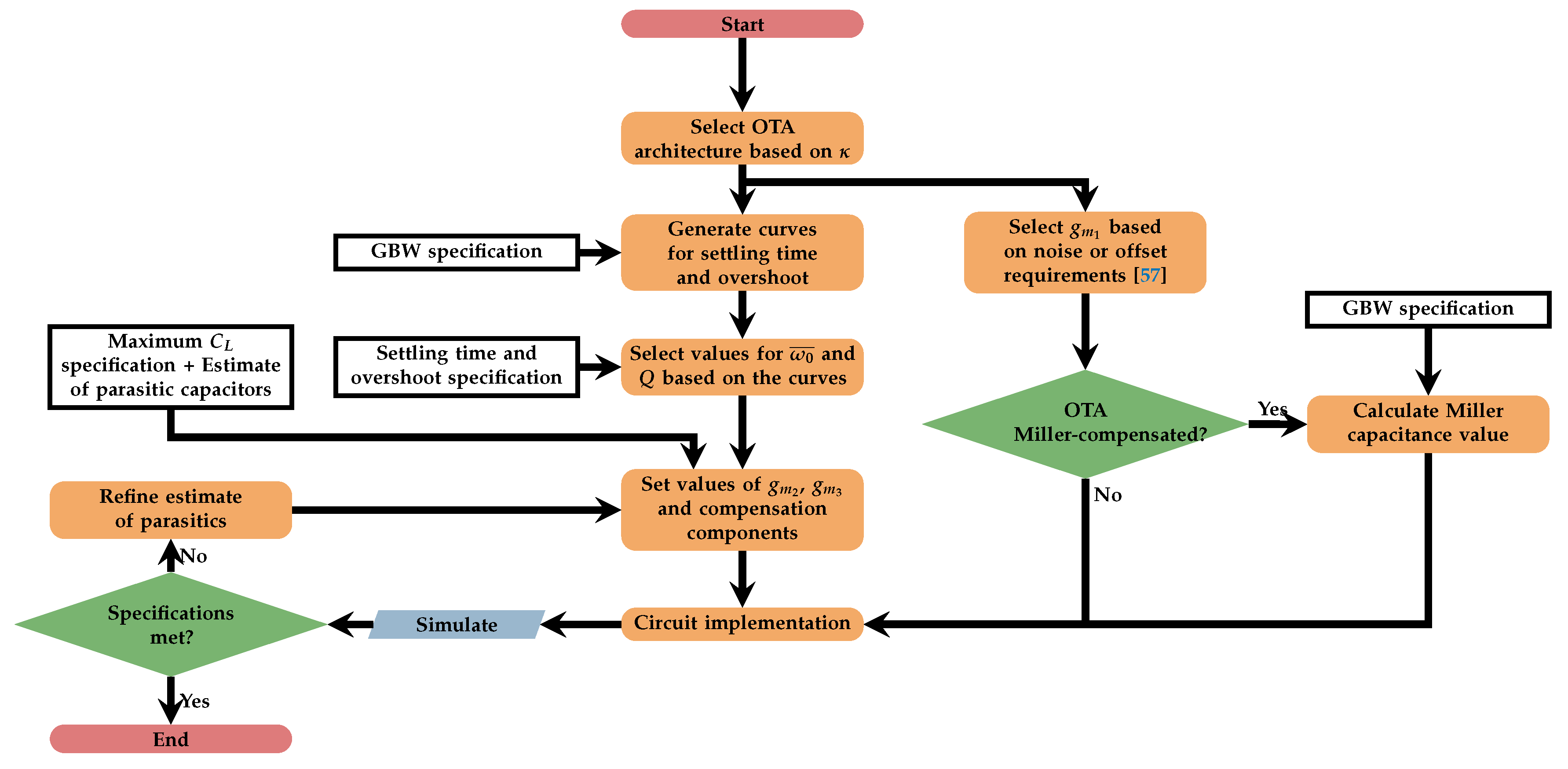
Figure 7 summarizes the design procedure discussed so far, starting from a specified GBW, maximum load capacitance, settling time and overshoot.
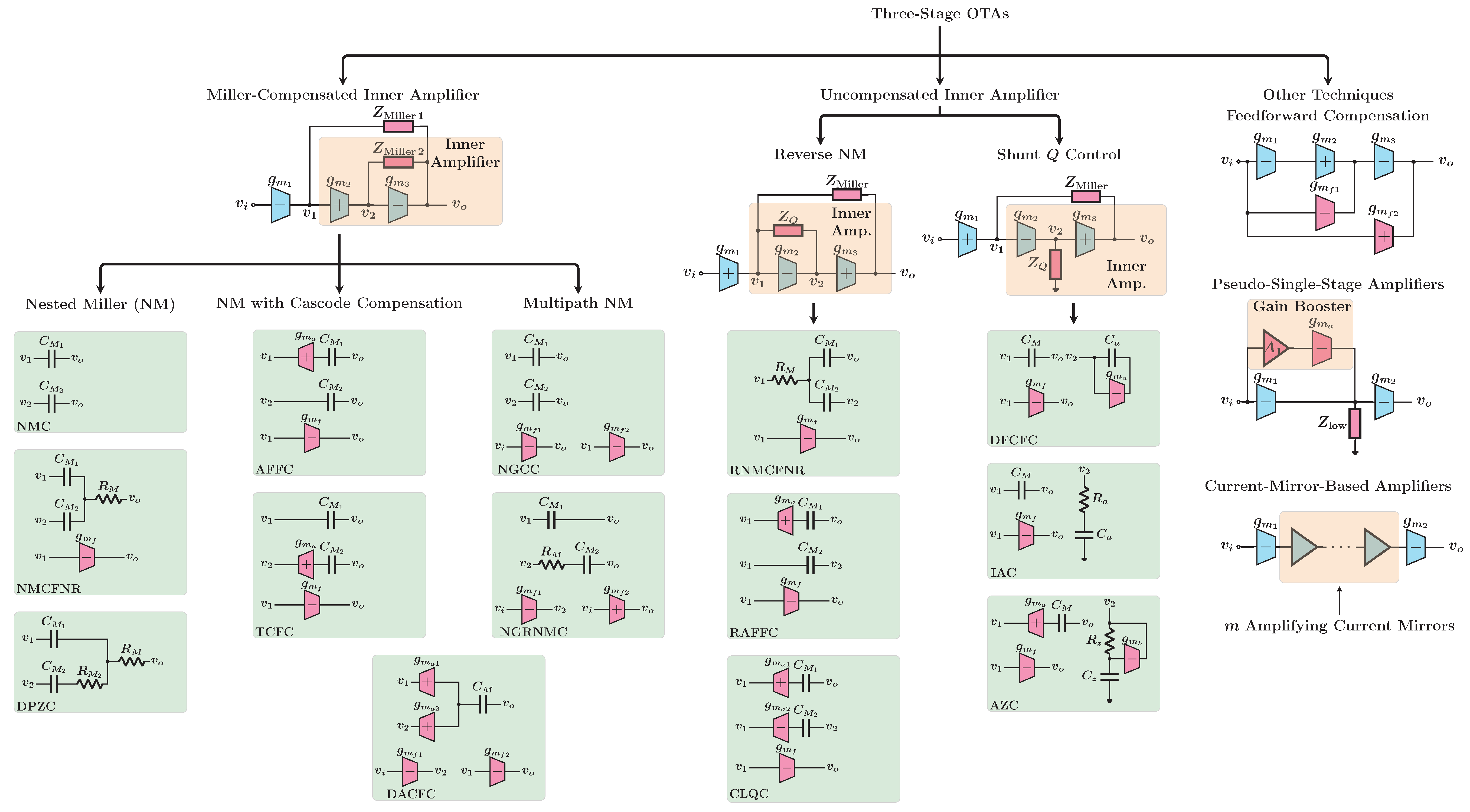
3. Classification of Multistage Amplifier Architectures
This section proposes a classification scheme for the existing compensation techniques of three-stage OTAs and outlines the common features in each technique. After the broad divisions are discussed briefly, each technique is examined via several example architectures with used as a FoM to compare them.
The classification scheme depends on whether the inner amplifier (as defined in [
54]) is Miller compensated. Specifically, let the transfer function of the two-stage inner amplifier be given by
, as shown in
Figure 8. In this case, the transfer function of the whole amplifier is given by
For a three-stage OTA,
will be second-order and may be expressed generically as
where
and
represent the voltage gains of the second and third stages, respectively, and
and
represent, respectively, the natural frequency and quality factor of the poles of the inner amplifier. Substituting Equation (
22) into Equation (
21), the following relations are found for
and
Q of the whole amplifier:
Using the example of the NGCC amplifier in
Figure 1 and neglecting
and
, one finds
so that we have
This demonstrates that, when the inner amplifier is Miller-compensated, the inner Miller capacitor controls the quality factor of the non-dominant poles and that decreasing the load capacitance reduces the quality factor.
On the other hand, if
were not present in
Figure 1, one can show that in this case
This means that, when the inner amplifier is not Miller compensated, the quality factor of the non-dominant poles depends on parasitic capacitors and increases as the load capacitor is decreased. This latter feature is responsible for increased gain peaking (and reduced gain margin) as the load capacitor is decreased in such architectures. This is because, at reduced loads the inner amplifier becomes unstable [
42].
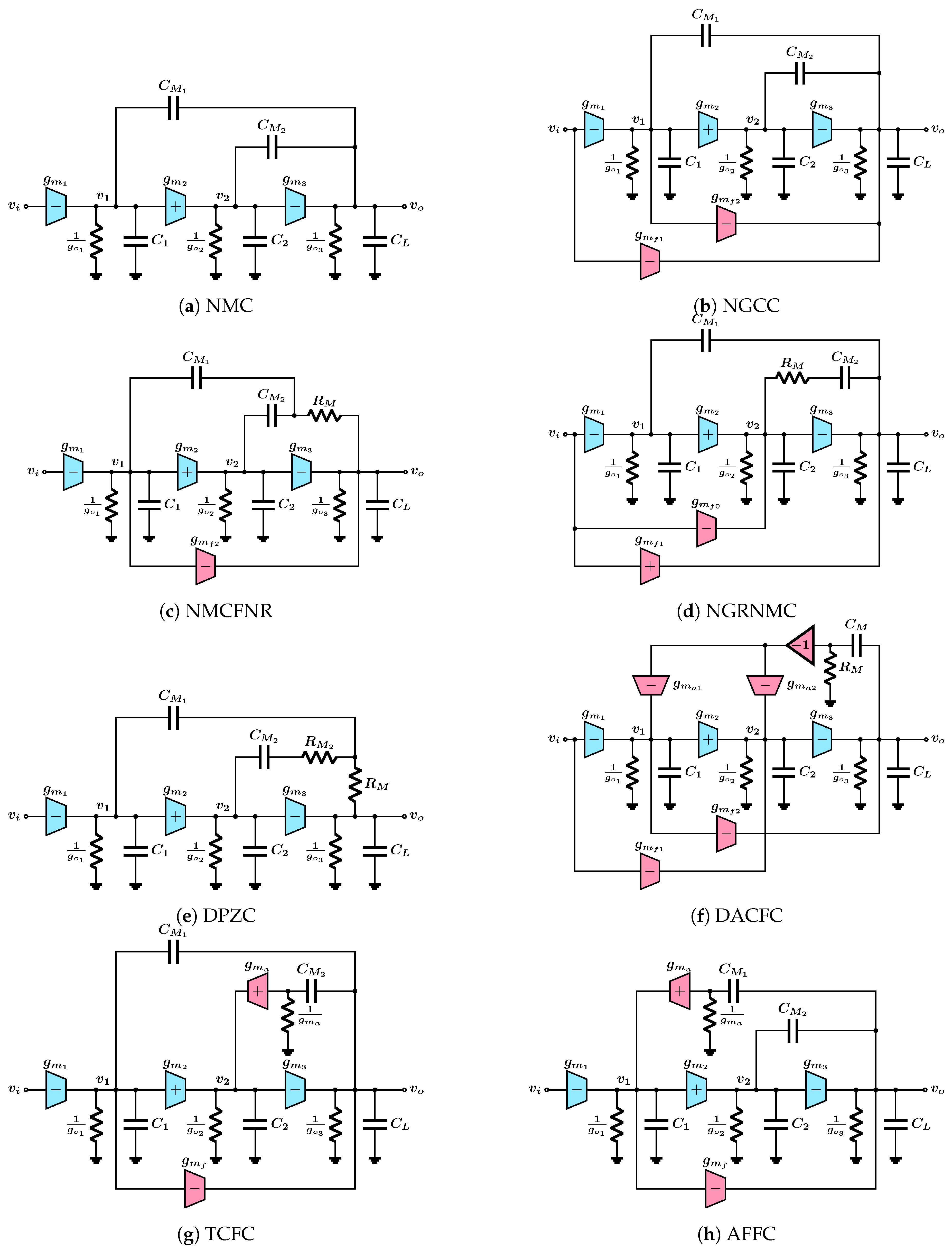
Figure 9 shows the classification scheme outlined above along with example architectures in each category. All architecture acronyms, along with citations of reference works are explained in
Table 5. Note from the figure that architectures where the inner amplifier is not Miller-compensated are sub-divided into reverse nested Miller architectures which rely on a feedback capacitor to control the quality factor of the inner amplifier poles and shunt
Q control architectures which use a shunt equivalent impedance to control the
Q factor. It should also be noted that some compensation architectures (such as DACFC [
28]) may fit into multiple categories while some architectures use techniques other than Miller compensation.
3.1. OTAs with Miller-Compensated Inner Amplifier
Figure 10 shows the compensation architectures that are studied in this section. The unifying features of this architecture type are discussed and the power efficiency of the different architectures is compared. Some typical applications that can best leverage these features are briefly touched upon as well.
Table 6 shows expressions for
,
and
Q for the compensation architectures of
Figure 10. As expected, all architectures (with the exception of DACFC) share the feature that
Q decreases as the load capacitance is decreased. DACFC is a special case because both compensation loops share the same capacitor, thus it does not fit the structure of
Figure 8.
Another interesting feature to note is that architectures that feature some form of cascode compensation (the bottom group in the table) have their
values enhanced by a factor that is the ratio of a Miller capacitor to a parasitic capacitor. This means that these compensation architectures tend to be more power-efficient as evidenced also by their
expressions being enhanced by similar factors with respect to their counterpart architectures (the top group in the table). This enhancement, observed in two-stage amplifiers as well, is due to one or both of the amplifier’s internal nodes avoiding the loading effect from the Miller capacitor (see, for example, [
11,
67]).
A common feature to these architectures is their reduced power efficiency at large capacitive loads. This may be seen both from the and the expressions. Large values of or (increasing means increasing and is desirable for improved settling time) require an increased power consumption.
The situation becomes worse due to the feedforward current through the inner Miller capacitor. This current creates a RHP zero in
and, by reference to Equation (
21) adds negative terms to the amplifier’s transfer function denominator requiring an increased value of
to avoid the amplifier going unstable (for example, to avoid
and
Q going negative in the case of NMC). Intuitively, it means that the current through
needs to be made a lot larger than the feedforward current through
. This translates into the
terms observed in the
factors of NMC and DPZC for instance. DPZC may overcome this problem by properly sizing the nulling resistor
to push this RHP zero to the LHP. Again, as may be observed from the
expressions, architectures that use cascode compensation to block the RHP zero through the inner Miller capacitor (DACFC and TCFC) or feedforward paths to cancel it (NGCC) do not suffer from this problem and are therefore more power-efficient.
As stated above, the
expressions allow us to compare architectures prior to designing them. With reference to
Table 6, the power efficiency advantage of NGCC over NMC is immediately obvious (in the sense that
is larger for the same
value). It is also observed that NMCFNR, NGRNMC and DPZC all have better
than NGCC for the same power consumption at the expense of added complexity. It should be noted be noted that the presence of resistive terms in these
expressions means that the designer can trade off chip area (and noise performance) to achieve better power efficiency by increasing the relevant resistor sizes. More subtly, it can be seen that NGRNMC allows is slightly more efficient than DPZC in that sense since its resistive terms are amplified by
which tends to be larger than the
terms seen in DPZC.
Moving towards the bottom group of the table, we observe the aforementioned enhancement to over the top group. Note that this enhancement is inherent to the architecture and does not require an extra power expenditure (the currentbuffers in cascode compensation are often embedded in the first and second stages and therefore exploit current reuse to achieve improved power efficiency at no additional power cost). More importantly, comparing expressions, it is evident that using cascode compensation in the inner loop leads to more power efficiency than using it in the outer loop.
Finally, note that DACFC is a special case in the sense that its value is independent of the load capacitance and should therefore have superior power efficiency to the other architectures in this category.
Applications that best leverage the properties of this type of architecture are applications where the maximum load capacitance is limited but where the amplifier should be stable at reduced load capacitance. A typical example of such an application are output-capacitor-free low-dropout (LDO) linear regulators that drive an on-chip power network with limited capacitance (see, for example, [
68]). Such applications fit with this type of architecture since
will be the transconductance of the LDO power transistor and will therefore be large by design. If settling speed and/or power efficiency are really critical, architectures with improved
such as DACFC or TCFC should be preferred.
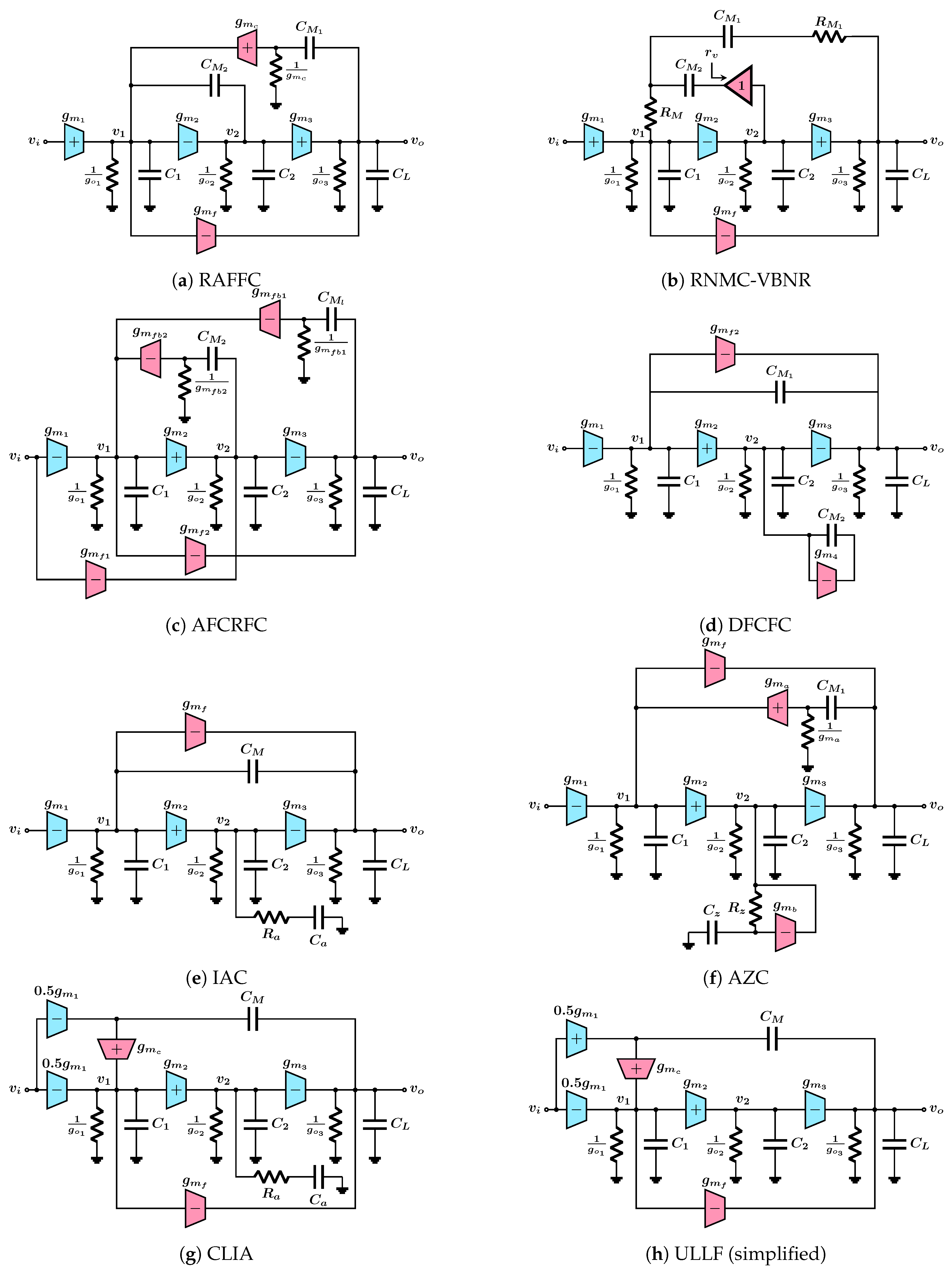
3.2. OTAs with Uncompensated Inner Amplifier
Figure 11 shows the compensation architectures that will be studied in this section. The discussion follows the same order as the previous section.
Table 7 shows expressions for
,
and
Q for the compensation architectures of
Figure 11.
First note that all architectures share the feature that Q increases as the load capacitance is decreased. This leads to increased gain peaking (and decreased gain margin) when the load is decreased as discussed above.
Note that the architectures discussed here are divided into the reverse nested Miller type and the shunt
Q control type. Amplifiers of the first type have their
values depend on the
Q control capacitor as it loads the output of the second stage. When shunt
Q control is used, there is no capacitor loading the output of the second stage, which leads to much higher values of
for the same power consumption. This is the main reason that such architectures are well-suited to drive ultra large capacitive loads (in the
range), as seen in recent publications [
11,
41,
42,
45].
Another feature common to all these architectures is that
is independent of the load capacitor, which means that the amplifier retains its power efficiency over a wide range of load capacitance. For this reason, these architectures are well-suited to drive a wide range of capacitive loads and can even have no upper limit on the capacitive load they can drive [
46].
On the other hand, the increased gain peaking at reduced load sets a lower limit on load capacitance. It should be noted that a strictly three-pole OTA from these architectures that has a gain margin defined by Equation (
17) will have a load-capacitance-independent gain margin and therefore no lower limit on load capacitance. In practice, however, this is not the case as practical OTAs have parasitic poles. To illustrate this, define
as the frequency of a parasitic pole such that the open loop transfer function of the OTA may be expressed as
If the Routh–Hurwitz criterion is applied to the
open-loop transfer function, the following condition is obtained
All the architectures in
Table 7 have
. Let
for some constant
. This transforms Equation (
28) into the condition
so that minimizing the lower limit on the load capacitance requires pushing the parasitic pole to a high frequency and having a low value for the constant
. This fact demonstrates the conflicting requirements for driving a wide range of load capacitance. Designing the amplifier for a given phase margin or settling time at a large value of
requires a large value of
and therefore a large value of
. Thus, pushing the upper limit on
automatically increases the lower limit as well and limits the overall range of loads the OTA can drive.
As before, the expressions allow us to compare architectures and we see that the shunt Q control types tend to have larger values of due to their inverse dependence on parasitic capacitors. Note also that the expressions allow us to see equivalences among architectures as well. By comparing the expressions for DFCFC and IAC, for instance, one sees that their efficiency is roughly equivalent when , which makes sense when their block diagrams are compared. This shows that the same performance can be obtained from either architecture and the designer should make the choice based on whether a larger area () or power () expenditure can be tolerated.
This type of architecture is best suited for applications that require driving a very wide range of load capacitors such as headphone drivers [
15,
46], LCD drivers [
11,
14], capacitive MEMS sensors [
14,
46], and LDO regulators [
46]. For LDO regulators, however, care should be taken that
is the gate capacitance of the power transistor and can therefore be substantially large.
3.3. Other Compensation Architectures
Some architectures do not use any Miller capacitors to achieve stability and are briefly surveyed here for the sake of completeness.
Feedforward compensation [
8] uses feedforward transconductance stages to generate zeros whose phase shift compensates that of the OTA poles thereby achieving stability. This architecture requires large power consumption in the feedforward stages to pull the zeros to low enough frequencies to be close to the poles.
The amplifiers in [
51,
52] achieve pseudo single-stage behavior by reducing the impedance of inner amplifier nodes to push the non-dominant poles to high frequencies. The required DC gain is restored by using shunt gain booster circuits, as shown in
Figure 9.
As an alternative approach, the amplifiers in [
49,
50] convert the input voltage into current then rely on cascading current amplification stages (amplifying current mirrors) to achieve the required DC gain. This approach leads to superior power efficiency when driving ultra large load capacitors, but the parasitic poles created by the cascade of current mirrors limit the load driving range as explained above.
5. Confirmation of Results through Transistor Simulations
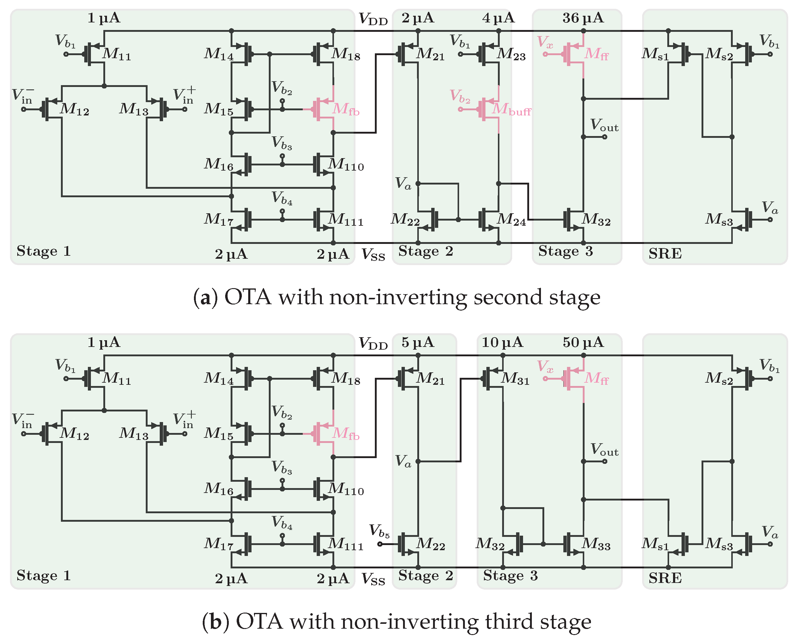
To further validate the above discussion, representative architectures are selected from the ones discussed above and are implemented at the transistor level in a standard 0.18 μm CMOS technology and their performance is compared via simulations using BSIM4, level 14 MOSFET models with the Spectre simulator ®. For a fair comparison, all OTAs are implemented with the same power budget whenever possible. The selected architectures for the comparison are NMC, NMCFNR, TCFC, RAFFC, IAC and CLIA.
5.1. Schematic Diagrams
To achieve a fixed power budget, all OTA implementations share the same core circuit with the exception of OTAs of the reverse nested Miller type, which require a non-inverting third stage. The circuit schematics for both types of OTA cores are shown in
Figure 12. Note that the magenta devices represent auxiliary devices for compensation.
is used as a feedback current buffer for architectures that employ cascode compensation.
serves a similar purpose for TCFC only and is removed in other architectures. Finally, the
devices implement a feedforward transconductance and, accordingly,
may be connected to the output of the third stage or to a bias voltage depending on whether the OTA has a feedforward transconductance or not.
In addition to the amplifier cores, the SRE described in [
46] is implemented to add additional charging/discharging current at the output node of
Figure 12a,b, respectively.
5.2. Selection of Circuit Parameters
The design is approached from the time domain perspective as discussed above. A settling time of less than 2 μs with a GBW of 1 MHz is targeted. An overshoot of less than 15% is also specified. The GBW value is set as a round figure approximation to the value achieved in several recent designs [
3,
42,
46]. With this value of GBW, the normalized settling time
is closest to the value 10 used as a heuristic in [
62]. Finally, an overshoot of 15% roughly corresponds to a second-order system with a damping factor of 0.5 [
65].
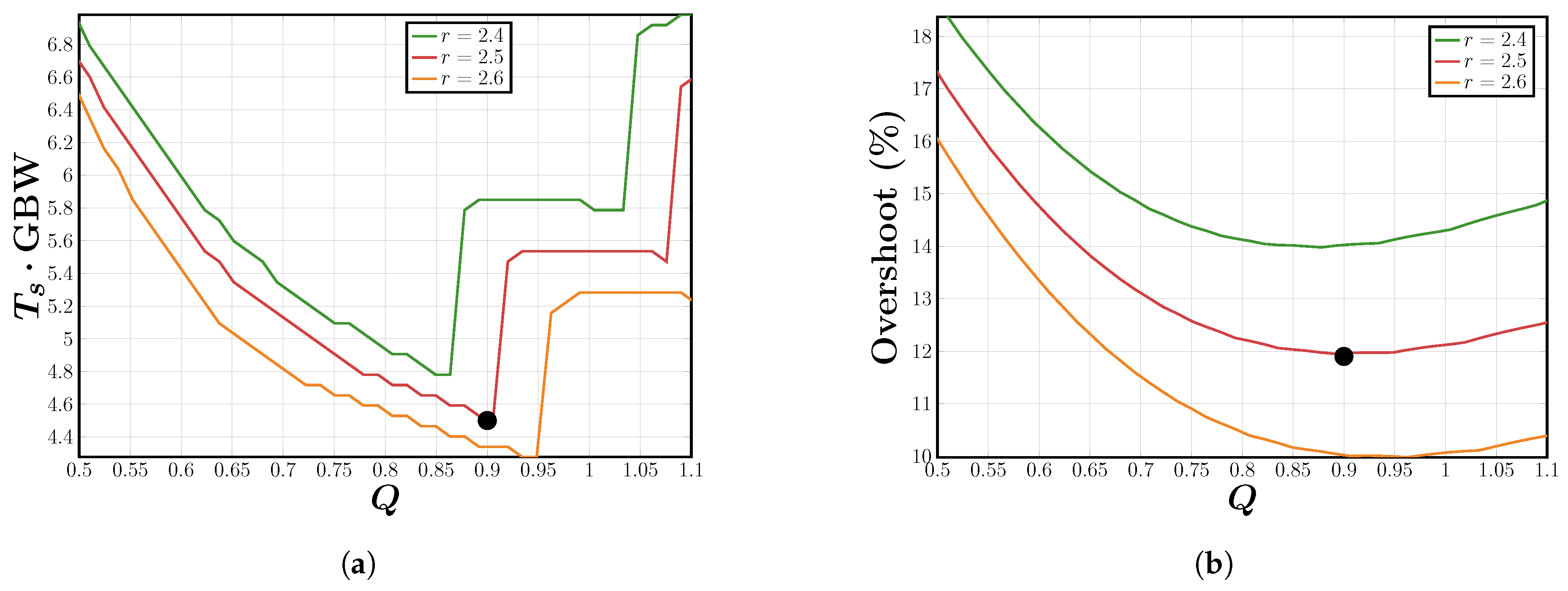
For each architecture, normalized curves similar to those in
Figure 4a,b are generated using numerical simulations in order to choose values of
and
Q that satisfy the performance targets. As an example,
Figure 13 shows the curves generated for the NMC architecture and the selected design point (
,
) where
was chosen to have an overshoot below 15% over a wide range of
Q values and
Q was chosen to optimize overshoot and settling time.
Using the selected values of
and
Q along with the expressions for
and
Q in
Table 6 and
Table 7, component values for the compensation network are chosen after
and
are fixed by the common OTA core. Since
and
are fixed beforehand in these example designs, the expressions for
and
Q are instead used to calculate the load capacitance that the OTA is capable of driving while achieving the given time domain performance.
5.3. Simulation Results
For simulations, the OTA cores were implemented in a standard 0.18 μm CMOS technology with targeted values for , and set to 10 μs, 50 μs and 500 μs, respectively. To account for routing and layout parasitics, the capacitances and were assumed to be 10 fF each (Based onextracted capacitance data from metal traces in the layout.).
For each architecture, the chosen compensation components are added and the resulting OTA is simulated to determine the range of load capacitance that each OTA can drive. The simulation results are shown in
Table 10.
The maximum load capacitance is reported as the load capacitance at which either the settling time exceeds 2 μs or the phase margin drops below 45° so that exceeding ringing appears in the step response. The minimum load capacitance, whenever a finite number is reported, is the minimum load capacitance below which the amplifier’s open-loop transfer function has a RHP pole due to the parasitic poles as explained above.
It should be noted that the differences in DC power consumption and core
values are due to the different biasing conditions according to whether the node
is connected to a constant bias voltage or to the output of the first stage. In addition, note that
of the CLIA architecture is considerably larger than the other cases because it was enhanced by a
amplifier (as explained in [
11]) (the gain-boostingamplifier was implemented using an ideal voltage-controlled voltage source with a gain of 33 dB for the purpose of this simulation to avoid disturbing the bias point of the core amplifier as much as possible) because a large value is needed for it to keep the OTA
Q to a low value and avoid gain peaking (as may be observed from
Table 7). The value of
had to be increased as well to achieve an acceptably large
.
The results confirm the observations made in previous sections. By comparing NMC, NMCFNR and TCFC, we note that adding the resistor improves the load driving capability only slightly while blocking the RHP zero in the inner amplifier leads to a more than 50 × improvement in the maximum drivable load capacitance.
When architectures with non-compensated inner amplifiers are used, the required auxiliary compensation capacitor decreases significantly. We note that the reverse nested Miller type amplifier does not exhibit the same efficiency as the other amplifiers as it keeps the internal node loaded with a large capacitor as explained above; in addition, one has to impose a minimum load capacitance on it for stability.
Finally, note that CLIA, a similar architecture to IAC, can achieve compensation using a much smaller physical resistor due to the added cascode compensation. The tradeoff is that a larger power consumption is needed to push the parasitic poles to high frequencies in this case since cascode compensation causes the inner amplifier to have a larger-order transfer function and to therefore be more susceptible to instability as the load capacitance is decreased.
Figure 14 shows the average of the rising and falling settling times, phase margin and gain margin as functions of the load capacitance for each architecture where it can be observed once again how a large phase margin is not necessary for good settling performance where the NMC architecture for example exhibits a settling time of 1 μs and an overshoot of 2% at a phase margin of about 40°. Furthermore, note how all architectures have a phase margin that increases with decreased load while the gain margin in architectures with non-compensated inner amplifiers stays constant or gets worse with decreased load capacitance as expected due to the increased gain peaking.
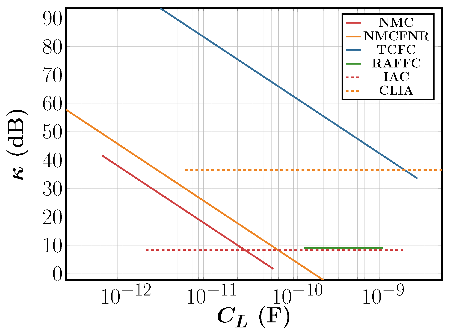
Finally, to confirm the utility of
,
Figure 15 plots the value of
as a function of load capacitance for each architecture. Where the superiority of the TCFC architecture is observed. Furthermore, the plot shows that, if the load capacitance is small, it is more power- efficient to use an architecture with Miller-compensated inner amplifier.
6. Conclusions
A thorough study of three-stage OTA architectures is presented, surveying a broad selection of state-of-the-art compensation techniques. The review emphasizes the point that designing these OTAs based on a target phase margin can lead to wasted power and degraded settling performance and that the main design targets need to be time domain performance parameters such as settling time and overshoot.
After discussing features common to all three-stage OTAs, a novel FoM is proposed to enable architecture selection prior to designing for a target application. In addition, a classification of the many different OTA architectures is proposed to expose the common features to each type of architecture and explain its suitability to different types of applications.
The observations presented were confirmed with transistor-level simulation results, which were found to agree with the expectations from the theoretical discussion.
Future extensions to this work should include a comparison of the linearity and noise performance of different OTA architectures from both an architecture perspective and a circuit perspective. Ideally, such an analysis should build on the work in [
56] and generalize it to multiple three-stage OTA architectures to identify desirable features in the compensation architecture from a non-linearity standpoint. A similar study should be carried out for noise performance as well.
Another avenue for future work is to compare the area requirements of different architectures and extend the verification methodology by laying out the different OTA designs and comparing post-layout simulation results.


