Review of GaN HEMT Applications in Power Converters over 500 W

Department of Electrical Engineering, CEECS, National United University, Miaoli 36063, Taiwan
*
Author to whom correspondence should be addressed.
Electronics 2019, 8(12), 1401; https://0-doi-org.brum.beds.ac.uk/10.3390/electronics8121401
Submission received: 18 October 2019
/
Revised: 12 November 2019
/
Accepted: 21 November 2019
/
Published: 23 November 2019
(This article belongs to the Special Issue Advances in Power Electronics Technologies for Renewable Energy Systems)
Abstract
:Because of the global trends of energy demand increase and decarbonization, developing green energy sources and increasing energy conversion efficiency are recently two of the most urgent topics in energy fields. The requirements for power level and performance of converter systems are continuously growing for the fast development of modern technologies such as the Internet of things (IoT) and Industry 4.0. In this regard, power switching devices based on wide-bandgap (WBG) materials such as silicon carbide (SiC) and gallium nitride (GaN) are fast maturing and expected to greatly benefit power converters with complex switching schemes. In low- and medium-voltage applications, GaN-based high-electron-mobility transistors (HEMTs) are superior to conventional silicon (Si)-based devices in terms of switching frequency, power rating, thermal capability, and efficiency, which are crucial factors to enhance the performance of advanced power converters. Previously published review papers on GaN HEMT technology mainly focused on fabrication, device characteristics, and general applications. To realize the future development trend and potential of applying GaN technology in various converter designs, this paper reviews a total of 162 research papers focusing on GaN HEMT applications in mid- to high-power (over 500 W) converters. Different types of converters including direct current (DC)–DC, alternating current (AC)–DC, and DC–AC conversions with various configurations, switching frequencies, power densities, and system efficiencies are reviewed.
1. Introduction
In recent years, due to the continuous growth of environmental concerns, there is limited room left for the development of fossil fuel-based power generation [1,2,3], and the rapid growth of global energy consumption resulted in fast development of various renewable energy (RE)-based power generation technologies, smart grids, optimal operation and control algorithms, hybrid energy storage systems, advanced energy conversion and management systems, and state-of-the-art power semiconductor devices for designing advanced power converters used in the abovementioned energy- and power-related systems. On the other hand, because of the global trend of carbon emission reduction, the penetration level of RE-based power generation is expected to keep growing. As a result, replacing fossil fuel with renewable and affordable energy sources and increasing the system efficiencies of energy conversion and power generation with better power switching devices and control techniques are some of the urgent research topics [4,5]. To support this development trend and achieve desired system performances, developing advanced power converters with better switching devices and control algorithms is extremely important. In addition, the requirements of power level, communication capability, and system performance of converters are also expected to continue growing in order to support the development of modern technologies such as Internet of things (IoT) and Industry 4.0. In this respect, advanced semiconductor switching characteristics, such as high switching frequency, lower switching losses, thermal capability, smaller sizes, and higher power densities, are required to realize the above goals.
To achieve the abovementioned application objectives and quality standards, technically utilizing wide-bandgap (WBG) gallium nitride (GaN)- and silicon carbide (SiC)-based switching devices and the related driving technologies is commonly believed to be the most promising approach. In fact, SiC-based Schottky diodes existed for more than a decade, and SiC-based metal–oxide–semiconductor field-effect transistors (MOSFETs), junction gate field-effect transistors (JFETs), and bipolar transistors (BJTs) appeared in recent years. In the aspect of potential SiC power switching devices for power converters, SiC MOSFETs of 10–15 kV/10–20 A are commercially available, which are more suitable for high-power and high-voltage applications with their intrinsic features in voltage and thermal conductivities. GaN is a direct-gap semiconductor, a wide-energy-gap material with performance advantages similar to SiC, but with greater cost control potential in practical applications. It has a unique heterojunction structure and two-dimensional electron gas. The high-electron-mobility transistor (HEMT) developed on this basis can achieve low on-resistance and high switching speed, which is more suitable for low- to medium-voltage and low- to medium-power applications. GaN HEMTs with 650 V/50 A and 900 V/15 A are commercially available. Driven by heavy demand for renewable power generations, e.g., photovoltaic (PV) inverters and power interfaces in wind turbine generators, energy storage systems, electric vehicles, and other industrial applications, it is believed that the emerging market for various advanced power converters based on GaN power devices will grow at a significant rate in the next decade. In the past eight years, there were a huge number of commercial reports and research papers regarding the application of WBG GaN- and SiC-based power switching devices published in the open literature. However, comprehensive research reports and technical review papers on GaN HEMTs, previously published in the open literature, mainly focused on fabrication, device characteristics, converter design examples, and other general applications. There is no review paper on their applications in various high-power converters. To compensate for this insufficiency and provide further research directions, this paper aims at giving the readers a wider comprehensive understanding of the capabilities and effectiveness of GaN HEMTs applied to mid- to high-power (over 500 W) converter applications, as well as key technologies, in terms of their intrinsic merit and potential. To build some background for this topic, the next section briefly addresses the characteristics, driving requirements, and commercially available products of GaN HEMTs. The third section focuses on the review of GaN HEMT application articles found in open literature since 2011. Reviewed types of power converters include direct current (DC)–DC, alternating current (AC)–DC, and DC–AC converters. Categories of the reviewed papers concerning various GaN-based converters presented in Section 3 are shown in Figure 1 and Table 1. Figure 2, Figure 3, Figure 4 and Figure 5 graphically present the distributions of reviewed papers with pie charts in terms of highest switching frequencies, highest output powers, efficiencies at highest output powers, and power densities, respectively. A conclusion is given in the last section.
2. GaN HEMT Background
Semiconductor devices are very commonly used in a variety of power conversion systems. Enhancing the power conversion efficiency means improving the overall energy utilization rate. Because Si-based power switches have low linearity in output capacitance, high output charge, high reverse recovery charge, and high gate charge, they are not expected to be used in designing advanced power converters meeting the required high system efficiencies and power densities [6]. WBG materials such as GaN and SiC offer substantial advantages over Si for power semiconductor applications, as shown in Figure 6.
As can be seen in Figure 6, SiC offers superior thermal conductivity, while GaN has the highest bandgap and electron mobility. Over the past few years, WBG material-based switching devices were intensively researched to achieve their full potential. These devices, with proper design, not only benefit existing power conversion systems but also provide new possibilities in improving some of the existing power electronic systems. SiC-based devices outperform Si-based devices tremendously in high-power (over 600 V) applications and are currently considered the most suitable devices for efficient power conversion at the abovementioned voltage level. However, quality material for SiC-based devices is quite limited and, thus, increasingly costly. As a result, GaN-based devices are considered potential alternatives to SiC-based devices in applications of low- to medium-level voltage. Commercially available GaN-based power switching devices offer an operating voltage ranging from 100 V to 1200 V, high switching frequency and operation temperature capabilities, and reduced switching losses. However, the very low threshold voltage (VGS_th) in normally off GaN devices is a technical problem in practical applications. Moreover, SiC-based devices still dominate applications with voltage levels over 1000 V [7,8].
GaN HEMTs are naturally on because of the two-dimensional electron gas (2DEG) that allows high current. Normally on GaN HEMTs, also known as depletion mode (D-mode) GaN HEMTs, can be turned off by applying negative VGS_th. Technical reports verify that various methods can be used to deplete the 2DEG path of a D-mode GaN HEMT and to realize the desired normally off switching characteristics. Commercially available normally off GaN HEMTs are divided into two types: enhancement mode (E-mode) and cascode configuration. E-mode GaN HEMT can be turned on by applying positive VGS_th. Generally, the sum of external resistance and driver output resistance should be designed as much larger than the internal resistance of an E-mode GaN HEMT in order to reduce the influence of internal resistance on the switching speed and reduce voltage overshoot. In practice, cooling is also crucial for further reducing conduction losses. In the aspect of driving E-mode GaN HEMT, the limit of peak driving voltage, the damping of driving charges, and the input/output propagation delay should be taken into consideration. Also, it is recommended to incorporate a Miller clamp, negative voltage source, and separate paths for turn-on and turn-off processes [9]. Cascode GaN HEMT combines a D-mode GaN HEMT and a normally off high-speed Si metal–oxide–semiconductor field-effect transistor (MOSFET) to realize a normally off characteristic, and it can be turned on by applying positive VGS_th on the Si MOSFET. For switching frequency over 100 kHz, it is recommended to use separate turn-on and turn-off paths, Kelvin source connection, ferrite beads, and minimized turn-off resistance and inductance of the driving loop [10]. Various driving circuits for GaN HEMTs were explored in References [9,10,11,12,13,14,15,16,17,18]. Discussion and designs for GaN HEMT driving circuits were provided in References [19,20,21]. The designs of special undervoltage lockout circuit and low-inductance driving circuits were discussed in References [22] and [23], respectively.
In the aspect of device specifications, current voltage ratings of commercial GaN HEMTs are up to 650 V, as shown in Table 2, where Vds represents drain-source voltage, Id represents drain-source current, VTH represents threshold voltage, Vgs represents gate-source voltage, Rds(on) represents on resistance, and Ciss represents input capacitance. Transphorm mainly produces 650-V cascode GaN HEMTs and evaluation boards for various applications based on their own GaN HEMTs. GaN System mainly produces 650-V and 100-V E-mode GaN HEMTs. Various GaN half-bridge evaluation boards are also commercialized for potential researchers. Texas Instruments (TI) and Silicon Labs produce both single-channel and dual-channel gate drivers suitable for GaN HEMTs, as shown in Table 3 and Table 4, respectively. TI also produces GaN switching modules that integrate GaN HEMTs with designed drivers as shown in Table 5.
3. GaN HEMT Applications in Power Converters
This section reviews power converter applications using GaN HEMTs. Reviewed types of power converters include DC–DC, AC–DC, and DC–AC converters.
3.1. DC–DC Converters
3.1.1. Isolated DC–DC Converters
Commonly used isolated DC-DC converters include phase-shifted full bridge (PSFB) converters, dual active bridge (DAB) converters, and LLC resonant converters. High voltage gain, good robustness, high efficiency, and wide operation temperature range are the design trends for DC–DC converters. Galvanic isolation is usually achieved by using transformers in isolated DC–DC converters, which is not an efficient strategy. Even so, with zero voltage switching (ZVS) or zero current switching (ZCS) techniques, more satisfactory efficiencies can be achieved [24].
The energy storage system (ESS) is one of the most important technologies for better utilizing the power generated from RE sources. Moreover, ESS can also assist in power quality (PQ) improvement by providing or absorbing active power. A DC–DC converter is often used to interface an ESS with one of its DC buses in the above PQ application cases. Xue, et al. carried out a series of studies on GaN-based isolated DC–DC converters for ESS applications. They firstly proposed a 200/12-V, 500-W, 100-kHz bidirectional converter prototype in Reference [25] for a stationary energy storage device (SESD) used in a 400-V DC microgrid (MG). This configuration utilized the free-wheeling diode for expanded operating range and increased overall efficiency. Then, they proposed a 380/12-V, 1-kW, 100-kHz converter prototype in Reference [26] for a battery ESS (BESS), where the ultrafast free-wheeling diode continued to play an important role; this converter was later used in Reference [27] for further loss analysis using a universal power loss predicting method. In [28], a non-modular high-voltage SiC-based dual-interleaved converter and a modular low-voltage GaN-based DC-DC converter operating at high switching frequency were investigated.
In Reference [29], the cross-side voltage ringing due to fast-switching GaN HEMTs in a GaN-based PSFB converter for battery charger applications was explored. It was suggested that increased transformer turn ratios can mitigate the overvoltage phenomena effectively and, thus, primary-side rms currents and the required voltage rating of the switching devices can be reduced. A 400/12-V, 1.4-kW, 100-kHz PSFB converter was used to verify the design approach. A capacitor-clamped, three-level converter with dual voltage outputs for battery aircraft charger application was proposed in Reference [30]. The charger could output either 28 V in LLC mode or 270 V in buck mode, selected using a jumper, to satisfy the two most common DC bus voltage requirements in airplanes. In LLC mode, the resonant frequency was twice the switching frequency of primary-side switches; for operating in buck mode, the frequency of the output inductor current was twice the switching frequency. This reduced the size of magnetic devices while maintaining a low switching loss. A 400/12-V, 1.5-kW, 500-kHz prototype was used to verify the proposed design operating principle. Hassan [31] compared the performance of GaN- and Si-based DAB converters for ESS applications. Boundary element and finite element methods (BEM and FEM) were demonstrated to be useful for the reduction of printed circuit board (PCB) layout parasitics and the design of required transformers. A 48/400-V, 2-kW, 200–400-kHz prototype was used to verify the superiority of GaN switching devices over Si switching devices. In Reference [32], the gate drive design considerations were discussed for high-voltage (HV) cascode GaN HEMTs. Switching characteristics of the chosen device and its influence were analyzed on a 380/310-V, 8.4-kW, 500-kHz bidirectional multi-channel buck/boost battery charger operating in critical conduction mode (CRM). A digital isolator-based driving architecture was proposed with discussions of PCB layout and package parasitics. A novel 400-V/12 V, 1-kW, 100-kHz, GaN-based bidirectional converter with 98.3% efficiency was designed in Reference [33] for an MG ESS based on a phase-shift-controlled modified DAB power stage. In both soft-switching and hard-switching modes, low power loss and high power density were achieved.
In electrical vehicle (EV) applications, the basic requirements for an on-board charger (OBC) include small size and low weight. As a result, higher efficiencies and frequencies are essential for smaller heat sinks and inductances. Ramachandran [34] designed a 130/52-V, 1-kW, 50-kH, 98.8% efficiency PSFB converter. ZVS was achieved by strategically increasing the magnetizing current in the transformer. GaN switches were paralleled to increase power level and reduce conduction loss. A 330/12-V, 2-kW, 1-MHz LLC series resonant converter (SRC) was built in Reference [35]. To decrease the current stress of the secondary synchronous rectifier and suppress output current ripple, multiphase interleaved LLC SRC was adopted. In Reference [36], a bidirectional battery charger for a plug-in hybrid EV (PHEV) was built. This work was focused on the design of a 250/250-V, 2.4-kW, 500-kHz DAB stage, taking into account the challenging conditions, e.g., wide battery voltage range and sinusoidal charging capability, elimination of large DC link capacitors. Here, 97.2% and 96.4% efficiencies were achieved at 1-kW and 2.4-kW outputs, respectively. Moreover, 98.2% efficiency was further realized at 1-kW output by integrating the inductor into the transformer. Skarolek and Lettl [37] proposed using a Z-source converter to simultaneously provide the isolation of tractive system from a flow battery and enable a wide-range voltage control at high efficiency. A 30–60-V-input, 3-kW, 100-kHz prototype was used to verify that the topology was suitable for this application and that GaN HEMTs indeed increased power density. A 400/180–430-V, 3.3-kW, 145–190-kHz series-resonant converter used for OBC was implemented in Reference [38]. This converter adopted reduced-frequency-range control, which improved the performance of series-resonant converters with wider input voltage range and/or output voltage range by substantially reducing their switching frequency. As a result, the size of the passive components was reduced. A prototype converter with Si-based switches operated with a switching frequency from 150 to 190 kHz exhibited maximum full-load efficiency of 97.41%; the corresponding frequency range and efficiency of the prototype converter with GaN switches were 145 to 190 kHz and 98.1%, respectively. In Reference [39], the design of an LLC resonant tank for EV OBC with wide-range output voltage was discussed. The integrated transformer structure was utilized to deliberately make the transformer leakage inductance larger to implement the series inductance. The required space between primary and secondary windings also reduced the common-mode electromagnetic interference (EMI) caused by displacement currents. The design was verified using a 390/340–510-V, 3.3-kW, 250-kHz LLC converter. Schülting et al. [40] explained the design of a compact 400/400-V, 3.7-kW, 500-kHz, 96% efficiency DAB converter in detail. A compact, lightweight, 120- or 240/14-V, 6.6-kW, 100-kHz, 96.6% efficiency three-port converter was proposed in Reference [41] for OBC applications, whereas a 10.5-kW/L power density was achieved in the prototype. Efficiency higher than that of a silicon-based counterpart was obtained in the results even at 2.5-fold higher switching frequency.
In the aspect of power distribution applications, Yu et al. [42] proposed a phase-shift-based power flow control scheme based on a triple active bridge (TAB) converter, which was used in a higher-reliability DC power distribution system based on a 500-W open-loop TAB converter [43]. With the proposed control method, smooth output waveforms were obtained. For RE-based power generation systems, the performances of GaN- and Si-based DAB converters as ESS interfaces were compared in Reference [9], in which a 48/400-V, 4-kW prototype was built to exhibit GaN HEMT’s superior performance to Si-based switching devices. In Reference [44], a 380-V/12-V, 800-W, 1-MHz, 97.6% efficiency LLC converter was proposed for high-output current applications. A 900-W/in3 high power density was achieved with a novel integrated planar matrix transformer, which integrated four elemental transformers into one magnetic core and utilized a simple implementation with four-layer print circuit board winding. In order to reduce core loss, flux cancellation was utilized in the magnetic plates. In addition, leakage and termination losses were minimized by integrating synchronous rectifiers (SRs) and output capacitors into the secondary winding. A modular multilevel converter (MMC) was proposed in Reference [45] to replace conventional converter topologies and realize high voltage and power density in anode discharge power modules (ADPMs) used in solar electric propulsion (SEP) systems. The proposed 200/600-V converter achieved a 2-kW output with the power density of 110 W/in3 and 83% full-load efficiency at 1-MHz switching frequency. In computer server applications, Fei et al. [46] discussed the history of LLC resonant converters and proposed a new matrix transformer structure and an optimization algorithm. A 400/12-V, 800-W, 1-MHz, 97.6% efficiency LLC converter was used to demonstrate and verify the proposed scheme. In Reference [47], a 230/130-V, 700-W, 85-kHz ZVS bridgeless active rectifier-based multi-resonant converter was presented for inductive power transfer (IPT) systems. The device losses of GaN HEMT-based LLC, DAB, and phase-shift quasi switched capacitor (QSC) converters for a 400/48-V, 1-kW, 500-kHz application were compared in Reference [48]. Test results showed that the phase-shift QSC circuit was a promising circuit candidate for DC power supply applications.
For other industrial applications, Yoo et al. [49] demonstrated a 300/14-V, 500-W, 100-kHz, >93% efficiency PSFB converter with a secondary synchronous rectifier. Issues regarding PCB layout and optimal dead time were discussed. The efficiency of the PSFB converter using GaN HEMTs was improved by more than 2% through the comparison of efficiencies with existing PSFB converters. In Reference [50], the performances of a direct drive and synchronous drive for HV cascode GaN devices were compared in a high-frequency LLC SRC. the zero reverse recovery charge and integrated protecting scheme made direct drive a more attractive design. A prototype of 390/12-V voltage conversion, 500-W power output, 400-kHz switching frequency, and 97.7% efficiency was demonstrated. A 380/12-V, 600-W, 750-kHz, 98% efficiency LLC converter was built in Reference [51] by utilizing symmetrical magnetic flux of the proposed half-turn transformer, whose minimum number of turns was only 0.5. Fei et al. [52] explored a special planar matrix transformer shielding technique for common-mode EMI noise suppression and efficiency improvement. Half of the shielding was used as the primary winding, which led to a successful improvement. A 400/12-V, 800-W, 1-MHz, 97.7% efficiency converter was built to test the method. A distributed energy storage device (DESD) was designed in Reference [53] based on a 400/12-V, 1-kW, 100-kHz bidirectional converter. The device integrated a 13.2-V Li-ion battery pack, the proposed converter, and a wireless communication system for achieving an expanded operation range, reduced switching loss and EMI, and increased total efficiency. In Reference [54], a 325/24-V, 1-kW, 100–250-kHz, 97.2% efficiency converter was demonstrated, where the problems of overvoltage and the selection of optimal RC snubber were investigated.
Ramachandran and Nymand designed an ultra-high-efficiency 130/52/50-V, 2.4-kW, 50-kHz full-bridge converters in Reference [55] by paralleling GaN HEMTs and adopting high-efficiency magnetics and synchronous rectification methods. The designed converter was later demonstrated in Reference [56]. A peak efficiency of 98.8% was measured at 1.3-kW output in the former prototype, and a power density of 7 kW/L and efficiency more than 98.5% over a wide range of output power were achieved with the latter prototype. In Reference [57], a 180/90-V, 1.65-kW, <300-kHz testbed was designed for flying capacitor multilevel (FCML) converters. Over 95% efficiency was obtained with the designed testbed. A 280–400/52-V, 3-kW, 350-kHz, 98.3% efficiency LLC resonant converter was demonstrated in Reference [58]. Later, a modified design example with optimized efficiency and extended input voltage range from conventional 340–400 V to 280–400 V was demonstrated in Reference [59]. The efficiency curves of the same converter with the switches replaced with CoolMos (IPB65R110CFD) were compared. Results showed that better efficiency can be obtained with E-Mode GaN switches. For common mode (CM) noise reduction, Li et al. [60] proposed a symmetrical resonant converter, where E-mode GaN HEMTs were used at the secondary side. A symmetrical PCB transformer structure was also proposed with simple system structure and without additional hardware. A 400-V-output, 6.6-kW, 500-kHz, 97.8% efficiency CLLC resonant converter prototype with 130 W/in3 power density was built to verify the design concept. In Reference [61], a 10-kW, 200–400-kHz, 97.9% efficiency high-power-density LLC resonant converter and a new switching cell were presented. The designed switching cell consisted of two paralleled E-mode GaN HEMTs. Further optimization was achieved with an integrated high-frequency litz-wire transformer.
To provide a quick overview of key performances reported in this review category, Table 6 summarizes the highest reported values in terms of switching frequencies, efficiencies, and power densities, separated by power levels.
3.1.2. Non-Isolated DC–DC Converters
In contrast to isolated DC–DC converters, non-isolated DC–DC converters are not designed with active galvanic isolation. Consequently, higher efficiency is more easily achieved; however, other technical approaches to deal with the problem of DC current injection become mandatory [24]. To provide timely test reports, three half-bridge evaluation boards manufactured by Transphorm were explained in References [62,63,64]. These evaluation boards provide simple buck or boost converters for basic study and can be operated at ~400-V input, ~400-V output, with a switching frequency of 100 kHz, and output powers of 1, 2.5, and 3.5 kW. In these design cases, four-layer PCB layouts were used, and input/output specifications and probing considerations were also addressed.
Non-isolated DC–DC converters for EV-related applications were discussed in References [11,65,66,67,68,69,70,71,72,73,74]. Moradisizkoohi et al. [65] proposed a half-bridge, three-port, three-level converter that could supply the critical loads using the energy stored in battery if photovoltaic (PV) generation was not available or insufficient. The converter allowed soft-switching and simple control algorithms. A 70–120/600-V, 1-kW, 50-kHz prototype was built, and design specifications were verified. In Reference [66], a 200-V and 100-V-input, 1.2-kW, 100-kHz three-level boost converter was built for fuel cell (FC) vehicle application. The converter was based on a three-level flying-capacitor switching cell and integrated with an LCCD output network, which yielded higher voltage gain and lower voltage stress for the switching devices. A 2-kW multi-level bidirectional buck-boost converter was built in Reference [67] for an EV plug-in charger. Because the voltage stress across the switches was reduced using the proposed topology, GaN HEMT technology could be used in the powertrain of the EVs to achieve satisfactory performance. Moradpour and Gatto [68] simulated a 400/60–200-V, 2-kW, 20–50-kHz two-phase SiC/GaN-based converter that satisfied the plug-in EV (PEV)’s high power rating range of 30–150 kW, and the complex multi-phase topology was avoided. A cascade controller was used to realize the design. In Reference [69], a 100/750-V, 2-kW, 50-kHz multi-level resonant bidirectional converter utilizing modular switched-capacitor was built. With the additional resonant branch connected to each switches-capacitor cell, soft switching was achieved. For hybrid vehicle applications, a 48/12-V, 3.5-kW, >200-kHz, 97.5% efficiency bidirectional converter that satisfies some features, e.g., light weight and compactness, was proposed in Reference [70]. Shojaieet al [71] evaluated a 650-V GaN HEMT for its switching and conduction performances in a bidirectional diode-less 400/200-V, 5-kW, 300-kHz, >99% efficiency converter with high power density. Boundary conduction mode (BCM) and soft turn-on enabled switching frequencies up to hundreds of kHz. In Reference [72], both SiC- and GaN-based switching devices were used to build a 300/600-V, 5–40-kW, 10-kHz two-phase (~20 kW per phase) interleaved bidirectional converter. WBG devices provided high-efficiency power conversion while avoiding the complexity of multi-phase topology. GaN on Si E-HEMT and Si MOSFET were compared in Reference [73] on a 360/500-V, 80-kW, 50- and 300-kHz converter of a Nissan Leaf EV. GaN HEMTs enabled extremely high-efficiency power conversion with fast-switching slew rates, higher than 150 V/ns, and their low reverse recovery charge reduced the switching loss significantly. For automotive active suspension applications, Song et al. [74] presented a 12/48-V, 2.8-kW, 300-kHz highly dynamic bidirectional converter to eliminate the additional 48-V batteries required for dynamic driving. The converter adopted a mixed feedforward/feedback design. A multiphase topology with latest GaN HEMTs achieved the desired high speed and efficiency.
For GaN HEMT application in RE-based power generation, attractive converter topologies include dual- or multi-input topologies, such as interleaved converters, because of the need to incorporate ESS and/or distributed generation (DG) systems. For the voltage mismatch between PV systems and DC link, Moradisizkoohi et al. [75] proposed a double-input three-level quasi-Z source converter (DITLQZC) to increase the voltage gain and reduce the voltage stress on the switches. Simulation of a 30–50-V (PV) and 50–100-V (battery)/380-V, 1-kW, 50-kHz DITLQZC verified the feasibility of the design. In Reference [76], cascode GaN HEMTs and a SiC Schottky diode were used to design a 150–200/120–380-V, 1-kW, 20–100-kHz, >96% efficiency converter for residential PV applications. The performances of cascode GaN HEMT and Si CoolMOS in an interleaved converter were compared in Reference [77] for efficiency assessment. A 200/400-V, 20–220-kHz converter was designed for this evaluation. It was shown that using GaN devices improved the efficiency for the switching frequencies of 30–270 kHz and the temperature range of 50–150 °C. Elsayad et al. [78] proposed a new three-level converter with universal input. A prototype of 200/100-V, 1.1- and 1.3-kW, 100-kHz converter was built to verify the design. In Reference [79], the performances of Si MOSFET-, Si insulated gate bipolar transistor (IGBT)-, SiC MOSFET-, and GaN HEMT-based two-level three-phase half-bridge converters in a small-scale permanent-magnet synchronous motor (PMSM)-based wind turbine generator (WTG) were compared. A 335-V output, 3-kW, 140-kHz converter with direct torque control (DTC) scheme was designed to emulate actual loads. A new PV system configuration based on sub-module integrated converters (subMICs) was proposed in Reference [80] to reduce the power loss due to mismatch effect among interconnected PV modules. A prototype consisting of three 420/20-V, 5-kW, 250-kHz subMICs was developed to verify the advantages of the proposed configuration.
For MG applications, Moradisizkoohi et al. [81] built a 15–30/400-V, 1-kW, 100-kHz soft-switched converter based on an integrated dual half-bridge which enabled high voltage gain. In the proposed design, a voltage multiplier stage was used to further increase the voltage gain, and clamp circuits were also used to achieve soft switching. In Reference [82], an 800/380-V, 2.5-kW three-level bidirectional converter used in a Robert Bosch DC-grid system was built. From both simulation and experimental results, it was observed that such a design was superior to a single 1200-V SiC MOSFET-based converter in terms of switching and conduction performances. Two paralleled GaN HEMTs enhanced the power capability. For high-frequency applications, the avalanche problem of Si MOSFET was explored in Reference [83], and zero voltage switching was achieved for cascode GaN HEMTs. This work analyzed the voltage distribution principle during the turn-off transition and the ZVS principle during the turn-on transition for cascode GaN HEMTs. The capacitance mismatch between the high-voltage normally on GaN switch and low-voltage Si MOSFET was solved by adding an extra capacitor to compensate for the mismatch. Theoretical analysis was validated through experiments on a 180/360-V, 600-W, 1-MHz converter.
For other applications, a 200/966-V, 900-W seven-level FCML converter was proposed in Reference [84] for high step-up (HSU) conversion. This configure was expected to exceed the limitations of conventional boost converters in terms of voltage gain and power density. Ahmad [85] compared the performances of a modified HSU converter and a cascaded boost converter for obtaining high voltage gain. Better efficiency was obtained with the cascaded boost converter at higher voltage gain, while higher power density and lower voltage stress on the switches were the HSU converter’s main advantages. A 400/200-V, 1-kW, 100-kHz converter was simulated, and a scaled-down hardware was also implemented. In Reference [86], the performance of GaN-, SiC- and Si-based switching devices were compared in a 100–200/33.3–600-V, 1-kW, 20–100-kHz converter with a SiC Schottky diode to reduce switching loss. The switching characteristics of GaN HEMT at a 20–150/300-V, 1.2-kW, 1-MHz synchronous converter were discussed in Reference [87]. At 1.2-kW output, 94% efficiency was achieved. Deck and Dick [88] designed a 12/48-V, 2-kW, 50- and 100-kHz four-phase interleaved bidirectional converter. A low-permeability nano-crystalline metal tape material was chosen for the four-phase coupled inductor, which yielded effective increase in power density. In Reference [89], the benefits of using GaN HEMTs in power electronic converter systems were demonstrated by using an optimized driving circuit for low conduction and switching losses in a 150–350/350-V, 2-kW, 16–144-kHz converter with maximum power point tracking (MPPT) control.
The performance of a 250/500-V, 2.3-kW, 100-kHz synchronous converter with ZVS and hard-switching modes was evaluated in Reference [90]. A physics-based model was firstly used to determine the switching losses, and system simulation was then performed to calculate the losses of specific elements. A peak efficiency of 99% was achieved at 1.4-kW output. Over 98% efficiencies were achieved with output powers above 400 W. GaN HEMT switching features were studied in Reference [91] with a ~400/~400-V, 2.5-kW, 50–250-kHz half-bridge converter. Three switching scenarios were analyzed: without anti-parallel diode, with anti-parallel SiC Schottky, and with additional parallel capacitor. Results showed significant reduction of switching power losses when the anti-parallel diode or additional capacitor was applied. The influence of dead time on power losses was also discussed, and an optimal solution was presented. In Reference [92], a 400/800-V, 3-kW, 100-kHz hard-switched converter was built to prove the capability of kV-class GaN on Si HEMTs. The efficiency exceeded 99% at 100-kHz switching frequency. A compact 360/400–500-V, 3-kW, 130-kHz bidirectional converter was proposed in Reference [93]. Zero voltage turn-on with negative Vgs was utilized. Further adjustment of the switching frequency to match the load current and output voltage further improved the efficiency over 99% for a wide output power range of up to 3 kW. A comprehensive analysis of design considerations for a 400/400-V, 4-kW, 400-kHz synchronous converter was presented in Reference [94]. Efficiency of about 96% was achieved. Siebke et al. [95] designed a 12–50/50-V, 5-kW, 500-kHz, 98% efficient four-phase interleaved bidirectional converter. A novel cooling system was integrated to improve the heat dissipation of the switching devices. A solution for paralleling GaN FETs in bridge power converters using drain ferrite beads and/or RC snubbers was provided in Reference [96] and verified with a 200/400-V, 2.5–5.5-kW, 100-kHz half-bridge circuit using two GaN FETs connected in parallel. The first solution was paralleling two TO-220/TO-247 devices directly, while the second was paralleling two TO-247 devices using drain ferrite bead.
To provide a quick overview of key performances reported in this review category, Table 7 summarizes the highest reported values in terms of switching frequencies, efficiencies, and power densities, separated by power levels.
3.2. AC–DC Converters
Conventional AC–DC converters, also known as rectifiers, are widely used in various industrial applications such as BESS, adjustable-speed drive (ASD), and uninterrupted power supply (UPS). The major disadvantages of such line-frequency-based converters include low power quality due to current harmonics, poor power factor, slow output-voltage regulation, low efficiency, and large size. As a result, switch-mode techniques are used to implement better AC–DC converters, e.g., pulse width modulation (PWM)-based AC–DC power converters designed with power factor correction (PFC) capabilities and better output voltage regulation features [97].
For EV applications, a 165/250-V, 1-kW, 500-kHz bidirectional PHEV battery charger based on normally off GaN-on-Si multi-chip module was built in Reference [98]. Efficiencies of 97% and 97.2% were achieved for the AC/DC stage and DC/DC stage, respectively, which yielded a total efficiency of 94.2%. The DC link capacitance could be further reduced with sinusoidal charging methods, yet the efficiency would drop to 92.0%. Elrajoubi et al. [99] simulated and explored a new low-voltage, high-current AC–DC converter topology for battery charging applications. The 120/48- or 60-V, 1.4-kW, 1-MHz converter was integrated with a totem pole PFC (TPPFC), an SRC, and a current-doubler rectifier (CDR) were used to improve the efficiency and compactness of the system. In Reference [12], a bidirectional converter was integrated with an LCL filter to achieve high efficiency. The dynamic oscillation phenomena were suppressed with state feedback control algorithms. A 2-kW, 620-kHz prototype was built with 98.127% peak efficiency. A 2.3-kW prototype of a bidirectional half-bridge power module was designed in Reference [13] for battery charger applications. Magnetic field canceling and Kelvin connection were used to minimize the required inductances. A high-efficiency continuous current mode (CCM) bridgeless TPPFC (BTPPFC) design was discussed by GaN Systems in Reference [100]. The motivation, operating principle, and design considerations of BTPPFC using GaN E-HEMT were highlighted with the test results. In the technical report, a 176–264/400-V, 3-kW, 65-kHz BTPPFC design example was presented, and the basic operating principle, test set-up, circuit schematics, and the eight-layer PCB layout were also discussed in detail. Avila et al. [101,102] explored GaN HEMTs for contactless battery charging applications. The proposed back-end PFC concept was compared with commonly used front-end PFC, and the performances of Si and cascode GaN switches were also compared. The proposed back-end PFC reduced primary-side power loss by 45% and overall volume by 40% at the cost of increased resonant inverter power losses due to an increased resonant current. A 3.2-kW contactless battery charger based on a 230/350–400-V, 100-kHz converter was used to verify the design concept.
The design of an integrated transformer and inductor for a 350-V output, 3.3-kW, 500-kHz DAB PHEV charger was discussed in Reference [103]. A small (3 μH) inductor was needed to achieve ZVS for the proposed DAB converter. As a result, the leakage inductance was utilized as the series inductor for the DAB, and the space between primary and secondary winding was arranged to store the leakage flux energy. The designed transformer had over 99.2% efficiency. The power density of the designed transformer was 6.3-fold that of the lumped transformer and inductor in a 50-kHz charger designed with Si-based power switches. Li et al. [104,105] proposed a 85–265-VAC/500–840-VDC/250–450-VBattery, 6.6-kW, >300-kHz, >96% efficiency bidirectional interleaved bridgeless totem-pole converter for OBC applications, in which variable DC-link voltage was used to track voltage fluctuation and SiC and GaN devices were used to optimize the design. Design of a 6.6-kW, CRM AC/DC converter with very high-frequency, high power-density, bidirectional OBC for PEVs was discussed in Reference [106]. A novel variable DC-link voltage system configuration was proposed to achieve high-frequency soft switching. A complete 320/250–450-V, 6.6-kW, >300-kHz OBC system was demonstrated with 37 W/in3 power density and over 96% efficiency. Liu et al. proposed an 80–260/200–450-V, 7.2-kW, 500-kHz indirect matrix converter-based EV charger and compared the performances of SiC and GaN switching devices in the designed converter [107], where the variable-switching frequency and variable-phase shift control algorithm was explained [108]. Although similar efficiencies of 97% to 98% were obtained from the two WBG devices, GaN yielded ~4 kW/L power density, higher than that of 3.3 kW/L for SiC. A novel energy-balanced variable-frequency-control method for input-series-output parallel (ISOP) modular EV fast-charging stations and a 50/200-V, 7.2-kW, 100–500-kHz DAB-based single-stage converter were proposed in Reference [109]. Both high efficiency and high power density were achieved by reducing one power stage and eliminating the large DC-link capacitor. The proposed topology could be used as a modular building block to scale up to 50 kW by connecting the input terminals in series and output terminals in parallel.
An 85–265/387-V, 4-kW, 66-kHz bridgeless TPPFC evaluation board designed by Transphorm was described in Reference [110]. Detailed circuit descriptions, circuit diagrams, and bills of materials were given. Using GaN FETs in the fast-switching leg of the circuit and low-resistance MOSFETs in the slow-switching leg of the circuit, separately, resulted in improved performance and efficiency. GaN devices were discussed in Reference [111] for their application in server power supply with integrated magnetics. A 1-kW, >1-MHz, 96% efficient server power supply was demonstrated using an interleaved CRM TPPFC module and an LLC resonant converter. An integrated device with all the magnetic components can greatly reduce EMI noises; thus, using a simple one-stage EMI filter was enough. A power density of more than 150 W/in3 was achieved with satisfactory performance. Wand et al. [112] demonstrated a 230/400-V, 600-W, 3-MHz, 98.5% efficiency converter. Results were presented to show that GaN HEMTs have great potential for high-frequency switching applications. In Reference [113], GaN TPPFC was demonstrated to be more efficient than Si PFC topologies. A prototype of 230/387 V, 1 kW, and 100 kHz was built to verify the desired performance. It was further suggested that, in order to reach 99% efficiency, it was required to adopt heat sinking and thermal interface material (TIM), minimize the inductance of the whole system, and employ advanced control algorithms. Two 230/390-V BTPPFCs with 1-kW and 2.4-kW power, were built in Reference [114], which reached a peak efficiency of 99% at 50 kHz and 98.8% at 100 kHz. The proposed circuits adopted effective methods to solve design challenges of current sensing and load voltage regulation. Two types of GaN HEMTs in TO220 and TO247 packages obtained from Transphorm were successfully utilized in the proposed TPPFC.
To provide a quick overview of key performances reported in this review category, Table 8 summarizes the highest reported values in terms of switching frequencies, efficiencies, and power densities, separated by power levels.
3.3. DC–AC Converters
3.3.1. Single-Phase DC–AC Converters
For single-phase DC–AC converters, because of the simplicity and rugged control scheme, PWM inverters were the most commonly used power converter for decades in applications such as UPS, motor drive, and induction heating with lower voltage (below 1000 V) and lower capacity (below 5 kW) [115,116,117].
Three single-phase inverter evaluation boards were manufactured and reported by Transphorm in References [118,119,120], respectively. These evaluation boards provide easy ways to evaluate performances and advantages of GaN HMETs in various inverter applications. Their respective specifications are as follows: ~400/√2 Vin, 1 kW, 100–200 kHz; ~420/~290 V, 3 kW, 50–200 kHz; and ~400/√2 Vin, 4.5 kW, 50–150 kHz. GaN transistors configured as a full bridge were the power modules in each of the inverters. The power switches were tightly coupled to gate drive circuits, and convenient communication connections were provided.
For RE-based power generation applications, an active damping resonance suppression method for a single-phase PV quasi-Z-source inverter (qZSI) was proposed in Reference [121]. The 150/120-V, 1-kW, 100-kHz prototype was used to verify the effectiveness of the method. A capacitance minimization control strategy for PV qZSI was proposed in Reference [122] to buffer double-frequency ripple energy. The proposed control strategy could minimize the capacitance requirement and achieve low-input-voltage double-frequency ripple. A 140–180/120-V, 1-kW, 100-kHz PV qZSI was built and used to verify the effectiveness of the proposed method. Kayiranga et al. [123] focused on abnormal operation state analysis and control of asymmetric impedance network-based PV qZSI. WBG devices at high frequency could reduce the impedance network significantly. However, the reduced qZSI impedance network would result in abnormal operation modes, in addition to frequency resonances, in a range of several kilohertz. A control method to suppress the resonance resulting from the reduced impedance network was proposed. A 140–225/120-V, 1-kW, 100-kHz prototype was used to verify the effectiveness of the proposed control method. A scalable cascaded Z-source inverter was presented in Reference [124] for grid-interactive PV applications. The comprehensive Z-source network was designed based on an innovative equivalent AC circuit model. Four cascaded 60–120/135-V, 750-W, 125-kHz Z-source inverter cells were used to build a 3-kW PV system. The proposed topology could also achieve independent MPPT control for each module, which led to improved energy harvesting capability. In Reference [125], benchmarks of Si IGBT, SiC MOSFET, and GaN HEMT power switches at 600-V class were conducted in a T-type inverter. Evaluated items included gate driver requirements, switching performance, inverter efficiency performance, heat sink volume, output filter volume, and dead-time effect for each technology. Results showed that GaN had the lowest gate driver losses above 100 kHz, and SiC had the lowest gate losses below 100 kHz. Among the three technologies, GaN had the best switching performance in a 700/230-V, 3.5-kW, 16–160-kHz inverter, which reached 97.3% efficiency. Heat sink volume of the converter could be reduced the most by switching from Si to GaN solution. Output filter volume could also be greatly reduced with the same increase in device power loss for GaN-based converters. Furthermore, harmonic distortion at output current was reduced using WBG devices.
For other industrial applications, a 400/250-V, 2-kVA, 100-kHz inverter was designed and implemented in Reference [126] for the Google Little Box Challenge. A 102-W/in3 power density was achieved. SiC and E-mode GaN HEMTs were compared in several topologies of inverter stage and different power decoupling solutions. A DC notch filter and a hard-switching full-bridge converter were combined as the proposed design for the prototype.
Kulkarni et al. [127] discussed the lower-order harmonic distortion of differential-mode Ćuk inverter and proposed to deal with this problem with a systematic low-complexity control design. A 30–50/120-V, 500-W, 100-kHz prototype was built. An ultra-low-inductance power cell design for a three-level active neutral point clamped (ANPC) inverter was presented in Reference [128]. Results of the 700/300-V, 1-kW, 10-kHz prototype verified the performance of the proposed design in terms of ultra-low inductance. The performance of a 165/165-V, 1-kW, 50-kHz full-bridge inverter was presented in Reference [129]. Unipolar sinusoidal PWM (SPWM) was used for the control strategy. The inverter could easily reach 96% efficiency or more within the range of 100 W to 1 kW. A 420/300-V, 1-kW, 260-kHz full-bridge inverter was proposed in Reference [130] to evaluate the advantages of GaN HEMTs. Synchronous reference frame proportional–integral (SRFPI)-based outer voltage control and inner inductor current control designed with a stationary reference frame were used in the inverter control system. Load current feedforward and repetitive control were used to prevent voltage distortion caused by nonlinear loads. Alatawi et al. [131] simulated a 380-V-input, 2-kW, 20- and 100-kHz transformer-less topology derived from an H5 inverter and then compared it with conventional H5 topology. Results showed that the proposed topology could significantly reduce conduction losses of the system. Si IGBT and GaN HEMTs were also compared in this work, where results showed a >5% increase in efficiency when GaN HEMTs were used. A three-level neutral point clamped (NPC) inverter was designed and implemented in Reference [132], in which a 700/240-V, 2-kVA, 100-kHz inverter prototype with simple low-cost three-level boot-strap driver circuits was built for validation. In Reference [133], a 450/240-V, 2-kW, 120-kHz, seven-level FCML inverter with an active energy buffer was built for the Google/IEEE Little Box Challenge. The active buffer decoupled twice-line-frequency power pulsation by a factor of eight compared to conventional passive decoupling capacitors while maintaining an efficiency of more than 99%. A power density of 216 W/in3 and a peak overall efficiency of 97.6% were achieved. In Reference [134], a fully GaN-based 700/230-V, 2-kW, 16–160-kHz three-level ANPC inverter was built and tested. The trade-off between heat sink and output filter volume was later discussed in Reference [135]. The obtained static and dynamic characteristics based on an inverter prototype showed excellent switching performance of GaN HEMTs under wide load current and temperature conditions. A 370/400-V, 2-kW, 100- and 250-kHz, 95% efficiency IPT system was presented in Reference [136]. The inverter was designed to ensure low switching losses while keeping the desired overshoot and slew rates. System efficiencies of 95% at 100 kHz and 92% at 250 kHz were achieved at 2-kW output power.
Ahmad et al. [137] discussed the benefit of grid-connected transformer-less inverters adopting GaN HEMTs and a modified PWM scheme. In the proposed 400/230-V, 2.3-kW, 200-kHz inverter prototype, the total harmonic distortion (THD) was reduced by 10%. The design and control of an 800/250-V, 3.1-kW, 120-kHz 13-level FCML inverter was discussed in Reference [138]. Custom integrated switching cells were designed to reduce commutation loop inductance and allow modular design. The frequency multiplication effect of FCML inverters allowed the output inductor of the inverter to be made exceptionally small while maintaining low THD due to the 1.44-MHz effective inductor ripple frequency. In Reference [139], natural air cooling and multilayer high-current PCB magnetics were used to design a 370/320-V, 5-kW, 50-kHz inverter with 98% efficiency. L. Liu et al. [140] presented a 400/240-V, 5-kW, 100-kHz grid-interactive, dual-paralleled inverter that was robust against shoot-through. GaN and Si devices were used to balance power loss and cost. A hybrid switching cell was proposed in Reference [141] using two GaN and two Si devices for a 400/400-V, 7.2-kW, 300-kHz full-bridge inverter. An enhanced gate drive loop ensured switching safety and performance. Modeer et al. [142] designed and implemented a 1000/380-V, 10–20-kW, 100-kHz, nine-level (~2.2 kW per level) flying capacitor multilevel inverter module. The innovative dual-sided layout reduced effective commutation loop inductance and enabled low ringing and fast switching. Detailed implemented components were listed. In Reference [143], high-level multilevel converter topologies were discussed and categorized into three types of designs based on their synthesis principles. A newly proposed internal parallelization (IP) topology with synthesis concept was used to further demonstrate the advantages of GaN HEMTs and realize a ~1500/690-V, 70-kW, 30-kHz inverter prototype.
To provide a quick overview of key performances reported in this review category, Table 9 summarizes the highest reported values in terms of switching frequencies, efficiencies, and power densities, separated by power levels.
3.3.2. Three-Phase DC–AC Converters
In recent years, three-phase inverters were widely used in a variety of applications, including energy conversion systems for distributed power generations, smart grids, energy storage systems, electric vehicles, and flexible AC transmission systems (FACTS) devices for power quality and power system control. Theoretically, a number of PWM schemes can be used in three-phase inverter systems to obtain variable voltages and frequencies. Two commonly used PWM schemes are carrier-based SPWM and space vector PWM (SVPWM) [144]. The performances of a GaN HEMT and a Si IGBT were compared in Reference [145] using a 200-V-output, 1.2-kW, 25–120-kHz motor drive inverter which comprised three half-bridge circuits (bridge legs). Optimized PCB layout guidelines were given. The higher switching frequencies of the GaN HEMT were shown to reduce the rotor losses in slotted and slot-less stator of high-speed permanent-magnet electric machines. Lautner and Piepenbreier [146] evaluated the switching behaviors of top and bottom GaN transistors in a three phase-leg configuration. A 200-V-output, 1.5-kW, 100-kHz inverter with 97% efficiency was built. Proper PCB layout and suitable gate resistance values yielded clean switching waveforms with less overshoots. Performances of high-frequency PWM in AC motor drive applications were discussed in Reference [147]. Advantages include high motor efficiency, fast control response, lower motor torque ripple, close-to-ideal sinusoidal motor current waveform, smaller filter size, lower cost filter, etc. A 321/212-V, 2-kW, 100-kHz six-in-one GaN module for variable frequency drive (VFD) application was demonstrated. A PWM inverter for an ASD was investigated in Reference [148] for its excellent performance in power and energy densities. Simulations clarified the relationship between carrier frequency of the PWM inverter and the volume of an electromagnetic compatibility (EMC) filter and the relationship between the carrier frequency and the volume of a cooling system. Simulation results showed that the total volume of the inverter system could be reduced by 81.6% at the carrier frequency of 300 kHz. A 400/200-V, 3.7-kW, 300-kHz prototype was built, and 70% total volume reduction of an EMC filter at 300-kHz carrier frequency compared to a 10-kHz carrier frequency was achieved. A compact isolated drive-by-microwave (DBM) half-bridge gate driver was developed in Reference [149] which drove GaN HEMTs with its constant low power consumption of 0.9 W at switching frequencies up to 1.0 MHz. The low power consumption was achieved by using the 2.4-GHz microwave wireless power transmission technique. A 5-kW, 10-kHz motor drive with over 94% efficiency was successfully demonstrated with the fabricated drivers. Uğur et al. [150] compared different topologies of inverters for modular motor drive and proposed an integrated modular motor drive (IMMD) in Reference [151]. It was found that parallel connected modules were better for size reduction, and a 540-V-input, 8-kW, 50-kHz, >98% efficiency two-level series/parallel voltage source inverter (VSI) was proposed for driving a PMSM.
A 700/230-V, 3.5-kW, 160-kHz inverter using two GaN transistors and two SiC transistors for PV applications was presented in Reference [152]. The proposed bidirectional switched NPC (BSNPC) inverter realized 99.2% efficiency at 16 kHz and 1.4 kW. Good efficiency could be maintained up to 160 kHz. The impact of SiC and GaN devices on output filter size and cooling requirements was also discussed. Here, 72% heat sink volume and 57% filter size reductions were achieved while maintaining very good efficiency. In Reference [153], GaN and SiC devices were compared for MW-scale qZS cascaded multilevel inverters (qZS-CMI). Two solutions were proposed and compared: a 650-V GaN E-HEMT with 650-V SiC Schottky diodes and a 1200-V SiC power modules with 1200-V SiC Schottky diodes. Results showed that the first solution showed lower power losses and costs per qZSI module. However, more modules (over 200) were needed to achieve the design goal of a 1-MW/11-kV system. As a result, the second solution was adopted because it resulted in lower total loss and cost. Trung and Akatsu [154] presented a 400-V-input, 10-kW, 13.56-MHz resonant inverter for wireless power transfer systems with optimized efficiency design. A 4-kW experimental system was tested with 96.5% efficiency. For EV applications, a T-type three-level topology using both GaN and Si devices was proposed in Reference [155] to enhance light load efficiency. To reduce the cost, GaN neutral clamping leg was disabled at full load. A 400/800-V, 150-kW (50 kW per phase), 10-kHz prototype was built and reduced turn-on and turn-off losses by 92% and 83%, respectively.
Gurpinar et al. [156] designed a 700-V-input, 1-kW, 10-kHz ultra-low-inductance power cell for an ANPC converter. The four-layered PCB design was used for maximizing GaN HEMT performance. The results verified the effectiveness and performance of the ultra-low-inductance design. In Reference [157], the efficiency characteristics and thermal performances of a 150-V-input, 1-kW, 100-kHz inverter was discussed. Various load conditions and ambient temperatures were simulated. Results showed the highest converter efficiency of 99.41%, which was 4.89% higher than that of the Si-based inverter. Cooling requirements were also greatly reduced because of the high efficiency of GaN devices. The effect of switching frequency on the performance of a two-level inverter was explored in Reference [158]. A compact 400-V-input, 1-kW, 500-kHz half-bridge module with ultra-low power-loop inductance was built and tested. According to a set of given requirements, CM and differential mode (DM) EMI filters for various switching frequencies were designed. Kapino et al. [159] implemented a carrier-based PWM in a 700/230-V, 10-kW, 100-kHz hybrid three-level ANPC VSI. Each leg consisted of two GaN HEMTs and four Si MOSFETs. Different load conditions were used to validate the digital implementation. A 500-V-input, 10-kW, 100-kHz half-bridge inverter was designed in Reference [160] for ultra-low parasitic inductance and strong cooling capability. A gate drive circuit with comprehensive protection function was integrated to achieve a 17.5-kW/L power density. In Reference [161], the filter design to reduce inductor current ripple was explored with a 650–700/230-V, 10-kW, 200-kHz three-level ANPC VSI, in which GaN HEMTs were adopted for the high-frequency side, and Si MOSFETs were used for the low-frequency side. Wang et al. [162] reported the development and applications of WBG devices and how WBG devices were expected to change the landscape of the power electronic industry with their capabilities. An example of a 10-kW three-phase inverter was demonstrated.
To provide a quick overview of key performances reported in this review category, Table 10 summarizes the highest reported values in terms of switching frequencies, efficiencies, and power densities, separated by power levels.
4. Conclusions
To provide engineers and researchers in the fields of power electronics and energy-related applications with timely technical information for the development of GaN HEMT technologies, this paper reviewed a total of 162 technical reports and research papers focusing on GaN HEMT applications in mid- to high-power (over 500 W) converters recently published in the open literature. Reviewed types of power converters were categorized into (1) DC–DC converters, including isolated and non-isolated converters, (2) AC–DC converters, and (3) DC–AC converters, including single-phase and three-phase converters. Performance achieved in various designed cases along with key technologies and novel control algorithms used was summarized with some technical comments. Based on the results reported in the reviewed articles, GaN HEMTs effectively enable medium-voltage, mid- to high-power converters to achieve much higher system efficiencies (up to 99.8%), switching frequencies (up to 13.56 MHz), power levels (up to 80 kW per module), and power densities (up to 9.5 kW/in3 and 19 kW/kg). Moreover, it was shown that converters designed with GaN HEMTs, having excellent temperature capabilities, are able to achieve a system with much higher power density compared with that designed with Si-based power switches. In this respect, the high potential of adopting and further developing the state-of-the-art GaN HEMT technology can be expected. It is also expected that GaN HEMT-based devices will better facilitate the trends of high-efficiency energy conservation, decarbonization of the transport sector through electrification, and high-efficiency smart grids.
Author Contributions
The corresponding author, C.-T.M. conducted the review work, rerified the technical contents and polished the final manuscript. Z.-H.G., a postgraduate student in the department of EE, NUU, performed the paper search, managed figures and checked the related data.
Funding
This research was funded by MOST, Taiwan, with grant numbers, MOST 108-2221-E-239-007 and MOST 107-2221-E-239-036 and the APC was funded by MOST 108-2221-E-239-007.
Acknowledgments
The author would like to thank the Ministry of Science and Technology (MOST) of Taiwan for financially support the energy related researches regarding key technologies and the design of advanced power and energy systems.
Conflicts of Interest
The authors declare no conflict of interest.
References
- Annual Energy Outlook 2018 with Projections to 2050. Available online: https://www.eia.gov/outlooks/aeo/pdf/aeo2019.pdf (accessed on 11 January 2019).
- International Energy Outlook 2018 (IEO2018). Available online: https://www.eia.gov/outlooks/ieo/ (accessed on 27 December 2018).
- International Energy Outlook 2018 Executive Summary. Available online: https://www.eia.gov/outlooks/ieo/executive_summary.php (accessed on 27 December 2018).
- Renewables 2018 Global Status Report. Available online: http://www.ren21.net/gsr-2018/ (accessed on 27 December 2018).
- Renewable Energy Statistics 2018. Available online: https://www.irena.org/publications/2018/Jul/Renewable-Energy-Statistics-2018 (accessed on 27 December 2018).
- Jones, E.A.; Wang, F.; Costinett, D. Review of commercial GaN power devices and GaN-based converter design challenges. IEEE J. Emerg. Sel. Top. Power Electron. 2016, 4, 707–719. [Google Scholar] [CrossRef]
- Spaziani, L.; Lu, L. Silicon, GaN and SiC: There’s room for all: An application space overview of device considerations. In Proceedings of the 2018 IEEE 30th International Symposium on Power Semiconductor Devices and ICs (ISPSD), Chicago, IL, USA, 13–17 May 2018. [Google Scholar]
- Viswan, V. A review of silicon carbide and gallium nitride power semiconductor devices. IJRESM 2018, 1, 224–225. [Google Scholar]
- Hassan, H.A. A GaN Based Dual Active Bridge Converter to Interface Energy Storage Systems with Photovoltaic Panels. Master’s Thesis, Miami University, Oxford, OH, USA, 2017. [Google Scholar]
- Pajnić, M.; Pejović, P.; Despotović, Ž.; Lazić, M.; Skender, M. Characterization and gate drive design of high voltage cascode GaN HEMT. In Proceedings of the 2017 International Symposium on Power Electronics (Ee), Novi Sad, Serbia, 19–21 October 2017. [Google Scholar]
- Shojaie, M.; Elsayad, N.; Tabarestani, S.; Mohammed, O.A. A Bidirectional Buck-boost Converter Using 1.3 kV Series-Stacked GaN E-HEMT Modules for Electric Vehicle Charging Application. In Proceedings of the 2018 IEEE 6th Workshop on Wide Bandgap Power Devices and Applications (WiPDA), Atlanta, GA, USA, 31 October–2 November 2018. [Google Scholar]
- Shu, W.; Li, S.; Lu, S. Bi-Directional and Single Phase AC-DC Converter with Integrated LCL Filter and GaN E-HEMTs. In Proceedings of the 2018 IEEE Transportation Electrification Conference and Expo (ITEC), Long Beach, CA, USA, 13–15 June 2018. [Google Scholar]
- Acuña, J.; Seidel, A.; Kallfass, I. Design and implementation of a Gallium-Nitride-based power module for light electro-mobility applications. In Proceedings of the 2017 IEEE Southern Power Electronics Conference (SPEC), Puerto Varas, Chile, 4–7 December 2017. [Google Scholar]
- Gui, Y. Gate Driver for Phase Leg of Parallel Enhancement-Mode Gallium-Nitride (GaN) Transistors. Master’s Thesis, Virginia Polytechnic Institute and State University, Blacksburg, VA, USA, 15 May 2018. [Google Scholar]
- Ng, W.T.; Yu, J.; Wang, M.; Li, R.; Zhang, W. Design Trends in Smart Gate Driver ICs for Power GaN HEMTs. In Proceedings of the 2018 14th IEEE International Conference on Solid-State and Integrated Circuit Technology (ICSICT), Qingdao, China, 31 October–3 November 2018. [Google Scholar]
- Li, B.; Zhang, R.; Zhao, N.; Wang, G.; Huo, J.; Zhu, L.; Xu, D. GaN HEMT Driving Scheme of Totem-Pole Bridgeless PFC Converter. In Proceedings of the 2018 IEEE International Power Electronics and Application Conference and Exposition (PEAC), Shenzhen, China, 4–7 November 2018. [Google Scholar]
- Wu, H.; Fayyaz, A.; Castellazzi, A. P-gate GaN HEMT gate-driver design for joint optimization of switching performance, freewheeling conduction and short-circuit robustness. In Proceedings of the 2018 IEEE 30th International Symposium on Power Semiconductor Devices and ICs (ISPSD), Chicago, IL, USA, 13–17 May 2018. [Google Scholar]
- Sun, B.; Zhang, Z.; Andersen, M.A.E. Review of Resonant Gate Driver in Power Conversion. In Proceedings of the 2018 International Power Electronics Conference (IPEC-Niigata 2018-ECCE Asia), Niigata, Japan, 20–24 May 2018. [Google Scholar]
- Lu, Y.; Zhu, J.; Sun, W.; Zhang, Y.; Hu, K.; Yu, Z.; Leng, J.; Cheng, S.; Zhang, S. A 600 V high-side gate drive circuit with ultra-low propagation delay for enhancement mode GaN devices. In Proceedings of the 2018 IEEE 30th International Symposium on Power Semiconductor Devices and ICs (ISPSD), Chicago, IL, USA, 13–17 May 2018. [Google Scholar]
- Yu, J.; Zhang, W.J.; Shorten, A.; Li, R.; Ng, W.T. A smart gate driver IC for GaN power transistors. In Proceedings of the 2018 IEEE 30th International Symposium on Power Semiconductor Devices and ICs (ISPSD), Chicago, IL, USA, 13–17 May 2018. [Google Scholar]
- Seidel, A.; Wicht, B. Integrated Gate Drivers Based on High-Voltage Energy Storing for GaN Transistors. IEEE J. Solid-State Circuits 2018, 53, 3446–3454. [Google Scholar] [CrossRef]
- Guo, W.; Shuai, D.U.; Bai, C.; Lei, L.; Zhu, Y. Design of a Low Temperature Drift Undervoltage Lockout Circuit-Used for GaN FET Power Driver IC. In Proceedings of the 2018 15th China International Forum on Solid State Lighting: International Forum on Wide Bandgap Semiconductors China (SSLChina: IFWS), Shenzhen, China, 23–25 October 2018. [Google Scholar]
- Sun, B.; Zhang, Z.; Andersen, M.A.E. Research of Low Inductance Loop Design in GaN HEMT Application. In Proceedings of the IECON 2018—44th Annual Conference of the IEEE Industrial Electronics Society, Washington, DC, USA, 21–23 October 2018. [Google Scholar]
- Tomaszuk, A.; Krupa, A. High efficiency high step-up DC/DC converters—A review. Bull. Pol. Acad. Tech. 2011, 59, 475–483. [Google Scholar] [CrossRef]
- Xue, F.; Yu, R.; Yu, W.; Huang, A.Q. GaN transistor based Bi-directional DC-DC converter for stationary energy storage device for 400 V DC microgrid. In Proceedings of the 2015 IEEE First International Conference on DC Microgrids (ICDCM), Bad Homburg, Germany, 7–10 June 2015. [Google Scholar]
- Xue, F.; Yu, R.; Guo, S.; Yu, W.; Huang, A.Q. Loss analysis of GaN devices in an isolated bidirectional DC-DC converter. In Proceedings of the 2015 IEEE 3rd Workshop on Wide Bandgap Power Devices and Applications (WiPDA), Blacksburg, VA, USA, 2–4 November 2015. [Google Scholar]
- Xue, F.; Yu, R.; Yu, W.; Huang, A.Q. Loss analysis of a high efficiency GaN and Si device mixed isolated bidirectional DC-DC converter. In Proceedings of the 2016 IEEE Applied Power Electronics Conference and Exposition (APEC), Long Beach, CA, USA, 20–24 March 2016. [Google Scholar]
- Frivaldsky, M.; Morgos, J. DC-DC Converter Design Issues for High-Efficient DC Microgrid. Commun. Sci. Lett. Uni. Zilina. 2019, 21, 35–41. [Google Scholar]
- Hoffmann, F.; Prasobhu, P.K.; Liserre, M.; Buticchi, G. Overcoming design challenges in low voltage GaN based PSFB battery charger. In Proceedings of the IECON 2018—44th Annual Conference of the IEEE Industrial Electronics Society, Washington, DC, USA, 21–23 October 2018. [Google Scholar]
- Ren, R.; Liu, B.; Jones, E.A.; Wang, F.F.; Zhang, Z.; Costinett, D. Capacitor-Clamped, Three-level GaN-Based DC–DC Converter with Dual Voltage Outputs for Battery Charger Applications. IEEE J. Emerg. Sel. Top. Power Electron. 2016, 4, 841–853. [Google Scholar] [CrossRef]
- Hassan, H.A.; Iuravin, E.; Cai, H.; Scott, M. A GaN based Dual Active Bridge Converter for Energy Storage Systems. In Proceedings of the 2018 IEEE Energy Conversion Congress and Exposition (ECCE), Portland, OR, USA, 23–27 September 2018. [Google Scholar]
- Zhang, W.; Huang, X.; Lee, F.C.; Li, Q. Gate drive design considerations for high voltage cascode GaN HEMT. In Proceedings of the 2014 IEEE Applied Power Electronics Conference and Exposition—APEC 2014, Fort Worth, TX, USA, 16–20 March 2014. [Google Scholar]
- Xue, F.; Yu, R.; Huang, A.Q. A 98.3% Efficient GaN Isolated Bidirectional DC-DC Converter for DC Microgrid Energy Storage System Applications. IEEE Trans. Ind. Electron. 2017, 64, 9094–9103. [Google Scholar] [CrossRef]
- Ramachandran, R.; Nymand, M. Design and analysis of an ultra-high efficiency phase shifted full bridge GaN converter. In Proceedings of the 2015 IEEE Applied Power Electronics Conference and Exposition (APEC), Charlotte, NC, USA, 15–19 March 2015. [Google Scholar]
- Pang, Z.; Ren, X.; Xiang, J.; Chen, Q.; Ruan, X.; Chen, W. High-frequency DC-DC converter in electric vehicle based on GaN transistors. In Proceedings of the 2016 IEEE Energy Conversion Congress and Exposition (ECCE), Milwaukee, WI, USA, 18–22 September 2016. [Google Scholar]
- Xue, L.; Mu, M.; Boroyevich, D.; Mattavelli, P. The optimal design of GaN-based Dual Active Bridge for bi-directional Plug-IN Hybrid Electric Vehicle (PHEV) charger. In Proceedings of the 2015 IEEE Applied Power Electronics Conference and Exposition (APEC), Charlotte, NC, USA, 15–19 March 2015. [Google Scholar]
- Skarolek, P.; Lettl, J. GaN Quasi Z-Source DC/DC Converter for Electric Vehicles with Redox Flow Batteries. In Proceedings of the 2018 International Conference on Applied Electronics (AE), Pilsen, Czech Republic, 11–12 September 2018. [Google Scholar]
- Liu, G.; Jang, Y.; Jovanović, M.M.; Zhang, J.Q. Implementation of a 3.3-kW DC–DC Converter for EV On-Board Charger Employing the Series-Resonant Converter with Reduced-Frequency-Range Control. IEEE Trans. Power Electron. 2017, 32, 4168–4184. [Google Scholar] [CrossRef]
- LLC Resonant Tank Design for 3.3 kW Electric Vehicle On-Board Charger with Wide-Range Output Voltage. Available online: https://www.transphormusa.com/en/document/design-guide-llc-resonant-tank-design-3-3kw-ev-board-charger-obc/ (accessed on 25 April 2017).
- Schülting, P.; Winter, C.; De Doncke, R.W. Design of a High-Frequency Dual-Active Bridge Converter with GaN Devices for an Output Power of 3.7 kW. In Proceedings of the 2018 International Power Electronics Conference (IPEC-Niigata 2018), Niigata, Japan, 20–24 May 2018. [Google Scholar]
- Su, G.J.; White, C.; Liang, Z. Design and evaluation of a 6.6 kW GaN converter for onboard charger applications. In Proceedings of the 2017 IEEE 18th Workshop on Control and Modeling for Power Electronics (COMPEL), Stanford, CA, USA, 9–12 July 2017. [Google Scholar]
- Yu, Y.; Masumoto, K.; Wada, K.; Kado, Y. A DC Power Distribution System in a Data Center using a Triple Active Bridge DC-DC Converter. IEEJ J. Trans. Ind. Appl. 2018, 7, 202–209. [Google Scholar] [CrossRef]
- Yu, Y.; Masumoto, K.; Wada, K.; Kado, Y. Power flow control of a triple active bridge DC-DC converter using GaN power devices for a low-voltage DC power distribution system. In Proceedings of the 2017 IEEE 3rd International Future Energy Electronics Conference and ECCE Asia (IFEEC 2017—ECCE Asia), Kaohsiung, Taiwan, 3–7 June 2017. [Google Scholar]
- Fei, C.; Lee, F.C.; Li, Q. High-Efficiency High-Power-Density LLC Converter with an Integrated Planar Matrix Transformer for High-Output Current Applications. IEEE Trans. Ind. Electron. 2017, 64, 9072–9082. [Google Scholar] [CrossRef]
- Barchowsky, A.; Kozak, J.P.; Grainger, B.M.; Stanchina, W.E.; Reed, G.F. A GaN-based modular multilevel DC-DC converter for high-density anode discharge power modules. In Proceedings of the 2017 IEEE Aerospace Conference, Big Sky, MT, USA, 4–11 March 2017. [Google Scholar]
- Fei, C.; Lee, F.C.; Li, Q. A new design paradigm for GaN based LLC converter. In Proceedings of the 2017 IEEE Southern Power Electronics Conference (SPEC), Puerto Varas, Chile, 4–7 December 2017. [Google Scholar]
- Mishima, T.; Morita, E. High-Frequency Bridgeless Rectifier Based ZVS Multiresonant Converter for Inductive Power Transfer Featuring High-Voltage GaN-HFET. IEEE Trans. Ind. Electron. 2017, 64, 9155–9164. [Google Scholar] [CrossRef]
- Hu, B.; Zhang, X.; Fu, L.; Li, H.; Abdullah, Y.M.; Wang, Y.; Liu, L.; Wang, J. Device loss comparison of GaN device based LLC, dual active bridge and phase shift quasi switched capacitor circuit. In Proceedings of the 2016 IEEE Energy Conversion Congress and Exposition (ECCE), Milwaukee, WI, USA, 18–22 September 2016. [Google Scholar]
- Yoo, J.G.; Joo, D.M.; Kim, H.B.; Kim, J.S. Implementation of a phase shift full-bridge converter for LDC using GaN HEMT. In Proceedings of the 2017 20th International Conference on Electrical Machines and Systems (ICEMS), Sydney, Australia, 11–14 August 2017. [Google Scholar]
- Yu, S.Y. Performance evaluation of direct drive high voltage Gallium-Nitride devices in LLC series resonant converters. In Proceedings of the 2016 IEEE 4th Workshop on Wide Bandgap Power Devices and Applications (WiPDA), Fayetteville, AR, USA, 7–9 November 2016. [Google Scholar]
- Li, S.; Rong, E.; Min, Q.; Lu, S. A Half-Turn Transformer with Symmetry Magnetic Flux for High-Frequency-Isolated DC/DC Converters. IEEE Trans. Power Electron. 2018, 33, 6467–6470. [Google Scholar] [CrossRef]
- Fei, C.; Yang, Y.; Li, Q.; Lee, F.C. Shielding Technique for Planar Matrix Transformers to Suppress Common-Mode EMI Noise and Improve Efficiency. IEEE Trans. Ind. Electron. 2018, 65, 1263–1272. [Google Scholar] [CrossRef]
- Xue, F.; Yu, R.; Yu, W.; Huang, A.Q. Distributed energy storage device based on a novel bidirectional Dc-Dc converter with 650V GaN transistors. In Proceedings of the 2015 IEEE 6th International Symposium on Power Electronics for Distributed Generation Systems (PEDG), Aachen, Germany, 22–25 June 2015. [Google Scholar]
- Zdanowski, M.; Kozdroj, K.; Rabkowski, J. Highly dynamic multiphase wide-bandgap DC-DC converter for automotive active suspension systems. In Proceedings of the 2017 Progress in Applied Electrical Engineering (PAEE), Kościelisko, Poland, 25–30 June 2017. [Google Scholar]
- Ramachandran, R.; Nymand, M. Effectively paralleling GaN FETs to achieve ultra-high efficiency in an isolated DC-DC converter. In Proceedings of the 2016 IEEE International Conference on Renewable Energy Research and Applications (ICRERA), Birmingham, UK, 20–23 November 2016. [Google Scholar]
- Ramachandran, R.; Nymand, M. Experimental Demonstration of a 98.8% Efficient Isolated DC–DC GaN Converter. IEEE Trans. Ind. Electron. 2017, 64, 9104–9113. [Google Scholar] [CrossRef]
- Chou, D.; Saathoff, E.K.; Pilawa-Podgurski, R.C.N. Design and implementation of a GaN-based multilevel converter testbed. In Proceedings of the 2017 IEEE Power and Energy Conference at Illinois (PECI), Champaign, IL, USA, 23–24 February 2017. [Google Scholar]
- Domb, M. High power density, high efficiency 380v to 52v LLC converter utilizing E-Mode GaN switches. In Proceedings of the PCIM Europe 2016; International Exhibition and Conference for Power Electronics, Intelligent Motion, Renewable Energy and Energy Management, Nuremberg, Germany, 10–12 May 2016. [Google Scholar]
- Amirahmadi, A.; Domb, M.; Persson, E. High power density high efficiency wide input voltage range LLC resonant converter utilizing E-mode GaN switches. In Proceedings of the 2017 IEEE Applied Power Electronics Conference and Exposition (APEC), Tampa, FL, USA, 26–30 March 2017. [Google Scholar]
- Li, B.; Li, Q.; Lee, F.C.; Yang, Y. A symmetrical resonant converter and PCB transformer structure for common mode noise reduction. In Proceedings of the 2017 IEEE Energy Conversion Congress and Exposition (ECCE), Cincinnati, OH, USA, 1–5 October 2017. [Google Scholar]
- Sun, B.; Burgos, R.; Boroyevich, D.; Bala, S.; Xu, J. 10 kW High Efficiency Compact GaN-Based DC/DC Converter Design. In Proceedings of the 2018 IEEE Energy Conversion Congress and Exposition (ECCE), Portland, OR, USA, 23–27 September 2018. [Google Scholar]
- TDPS1000E0E10 Half-Bridge Evaluation Board. Available online: https://media.digikey.com/pdf/Data%20Sheets/Transphorm%20PDFs/TDPS1000E0E10-KIT.pdf (accessed on 24 February 2017).
- TDHBG2500P100: 2.5 kW Half-Bridge Evaluation Board. Available online: https://www.transphormusa.com/en/document/tdhbg2500p100-user-guide/ (accessed on 24 February 2017).
- TDPS3500E0E10 Half-Bridge Evaluation Board. Available online: http://www.datasheetarchive.com/whats_new/4664bb820fb146bc25b22a40a6417ff0.html (accessed on 24 February 2017).
- Moradisizkoohi, H.; Elsayad, N.; Mohammed, O. Experimental Verification of a GaN-Based Double-Input Soft-Switched DC/DC Converter for Hybrid Electric Vehicle Application. In Proceedings of the 2018 IEEE Industry Applications Society Annual Meeting (IAS), Portland, OR, USA, 23–27 September 2018. [Google Scholar]
- Elsayad, N.; Moradisizkoohi, H.; Mohammed, O. A New Three-Level Flying-Capacitor Boost Converter with an Integrated LC2D Output Network for Fuel-Cell Vehicles: Analysis and Design. Inventions 2018, 3, 61. [Google Scholar] [CrossRef]
- Moradisizkoohi, H.; Elsayad, N.; Berzoy, A.; Lashway, C.R.; Mohammed, O.A. A multi-level bi-directional buck-boost converter using GaN devices for electric vehicle applications. In Proceedings of the 2017 IEEE Transportation Electrification Conference and Expo (ITEC), Chicago, IL, USA, 22–24 June 2017. [Google Scholar]
- Moradpour, M.; Gatto, G. Controller Design of a New Universal Two-Phase SiC-GaN-Based DC-DC Converter for Plug-in Electric Vehicles. In Proceedings of the 2018 IEEE 18th International Power Electronics and Motion Control Conference (PEMC), Budapest, Hungary, 26–30 August 2018. [Google Scholar]
- Moradisizkoohi, H.; Elsayad, N.; Mohammed, O.A. A resonant Bi-directional buck-boost converter with distributed voltage stress using eGaN HEMTs. In Proceedings of the 2017 IEEE 5th Workshop on Wide Bandgap Power Devices and Applications (WiPDA), Albuquerque, NM, USA, 30 October–1 November 2017. [Google Scholar]
- Li, B.; Qin, W.; Yang, Y.; Li, Q.; Lee, F.C.; Liu, D. A High Frequency High Efficiency GaN Based Bi-Directional 48V/12V Converter with PCB Coupled Inductor for Mild Hybrid Vehicle. In Proceedings of the 2018 IEEE 6th Workshop on Wide Bandgap Power Devices and Applications (WiPDA), Atlanta, GA, USA, 31 October–2 November 2018. [Google Scholar]
- Kloetzer, S.; Mueter, U.; Fahlbusch, S.; Hoffmann, K.F. Compact Diode-less Bidirectional GaN Based Buck Converter for Mobile DC-DC Applications. In Proceedings of the PCIM Europe 2017; International Exhibition and Conference for Power Electronics, Intelligent Motion, Renewable Energy and Energy Management, Nuremberg, Germany, 16–18 May 2017. [Google Scholar]
- Moradpour, M.; Gatto, G. A New SiC-GaN-Based Two-Phase Interleaved Bidirectional DC-DC Converter for Plug-In Electric Vehicles. In Proceedings of the 2018 International Symposium on Power Electronics, Electrical Drives, Automation and Motion (SPEEDAM), Amalfi, Italy, 20–22 June 2018. [Google Scholar]
- Attia, Y.; Youssef, M. GaN on silicon E-HEMT and pure silicon MOSFET in high frequency switching of EV DC/DC converter: A comparative study in a nissan leaf. In Proceedings of the 2016 IEEE International Telecommunications Energy Conference (INTELEC), Austin, TX, USA, 23–27 October 2016. [Google Scholar]
- Song, D.; Schwaiger, K.; Korte, C.; Stark, C.; Luetje, T.; Jaensch, M.; Goetz, S. Highly dynamic multiphase wide-bandgap DC-DC converter for automotive active suspension systems. In Proceedings of the 2017 IEEE 3rd International Future Energy Electronics Conference and ECCE Asia (IFEEC 2017—ECCE Asia), Kaohsiung, Taiwan, 3–7 June 2017. [Google Scholar]
- Shojaie, M.; Elsayad, N.; Tabarestani, S.; Mohammed, O.A. A Double-Input Three-Level Quasi-Z Source Converter Using GaN Switches with Reduced Voltage Stress for Multiple Energy Interface. In Proceedings of the 2018 IEEE 6th Workshop on Wide Bandgap Power Devices and Applications (WiPDA), Atlanta, GA, USA, 31 October–2 November 2018. [Google Scholar]
- Alharbi, S.S.; Alharbi, S.S.; Al-bayati, A.M.S.; Matin, M. A highly efficient non-isolated DC-DC buck-boost converter with a cascode GaN-FET and SiC-Schottky diode. In Proceedings of the 2017 IEEE Conference on Technologies for Sustainability (SusTech), Phoenix, AZ, USA, 12–14 November 2017. [Google Scholar]
- Alharbi, S.S.; Alharbi, S.S.; Matin, M. Effects of Gallium Nitride (GaN) Cascode FETs on the Efficiency of an Interleaved DC-DC Converter. In Proceedings of the 2018 IEEE International Conference on Electro/Information Technology (EIT), Rochester, MI, USA, 3–5 May 2018. [Google Scholar]
- Elsayad, N.; Moradisizkoohi, H.; Mohammed, O.A. A Three-Level Boost Converter with an Extended Gain and Reduced Voltage Stress using WBG Devices. In Proceedings of the 2018 IEEE 6th Workshop on Wide Bandgap Power Devices and Applications (WiPDA), Atlanta, GA, USA, 31 October–2 November 2018. [Google Scholar]
- Piriienko, S.; Neuburger, M.; Ammann, U.; Balakhontsev, A.; Thrimawithana, D.J.; Cheng, P.W. Evaluation of the Small-Scale Wind Turbine Converter’s Efficiency Built with Various Types of Semiconducting Devices. In Proceedings of the 2018 IEEE 3rd International Conference on Intelligent Energy and Power Systems (IEPS), Kharkiv, Ukraine, 10–14 September 2018. [Google Scholar]
- Khan, O.; Xiao, W.; Moursi, M.S.E. A new PV System configuration based on Submodule integrated Converters. IEEE Trans. Power Electron. 2017, 32, 3278–3284. [Google Scholar] [CrossRef]
- Moradisizkoohi, H.; Elsayad, N.; Mohammed, O. A Soft-Switched DC/DC Converter Using Integrated Dual Half-Bridge with High Voltage Gain and Low Voltage Stress for DC Microgrid Applications. Inventions 2018, 3, 63. [Google Scholar] [CrossRef]
- Lu, J.; Bai, H.K.; Averitt, S.; Chen, D.; Styles, J. An E-mode GaN HEMTs based three-level bidirectional ‘DC converter used in Robert Bosch DC-grid system. In Proceedings of the 2015 IEEE 3rd Workshop on Wide Bandgap Power Devices and Applications (WiPDA), Blacksburg, VA, USA, 2–4 November 2015. [Google Scholar]
- Huang, X.; Du, W.; Lee, F.C.; Li, Q.; Liu, Z. Avoiding Si MOSFET avalanche and achieving zero-voltage switching for cascode GaN devices. IEEE Trans. Power Electron. 2016, 31, 593–600. [Google Scholar] [CrossRef]
- Liao, Z.; Lei, Y.; Pilawa-Podgurski, R.C.N. A GaN-based flying-capacitor multilevel boost converter for high step-up conversion. In Proceedings of the 2016 IEEE Energy Conversion Congress and Exposition (ECCE), Milwaukee, WI, USA, 18–22 September 2016. [Google Scholar]
- Ahmad, B.; Kyyra, J.; Martinez, W.H. Efficiency Optimization of Interleaved High Step-Up Converter. In Proceedings of the 9th International Conference on Power Electronics, Machines and Drives (PEMD 2018), Liverpool, UK, 17–19 April 2018. [Google Scholar]
- Al-bayati, A.M.S.; Alharbi, S.S.; Alharbi, S.S.; Matin, M. Design and performance evaluation of a DC-DC buck-boost converter with cascode GaN FET, SiC JFET, and Si IGBT power devices. In Proceedings of the 2017 North American Power Symposium (NAPS), Morgantown, WV, USA, 17–19 September 2017. [Google Scholar]
- Hughes, B.; Lazar, J.; Hulsey, S.; Zehnder, D.; Matic, D.; Boutros, K. GaN HFET switching characteristics at 350V/20A and synchronous boost converter performance at 1MHz. In Proceedings of the 2012 Twenty-Seventh Annual IEEE Applied Power Electronics Conference and Exposition (APEC), Orlando, FL, USA, 5–9 February 2012. [Google Scholar]
- Deck, P.; Dick, C. Ultra Compact 2 kW 12 V–48 V Converter Using a 4-Phase Coupled Inductor. In Proceedings of the PCIM Europe 2018; International Exhibition and Conference for Power Electronics, Intelligent Motion, Renewable Energy and Energy Management, Nuremberg, Germany, 5–7 June 2018. [Google Scholar]
- Hensel, A.; Wilhelm, C.; Kranzer, D. Application of a new 600 V GaN transistor in power electronics for PV systems. In Proceedings of the 2012 15th International Power Electronics and Motion Control Conference (EPE/PEMC), Novi Sad, Serbia, 4–6 September 2012. [Google Scholar]
- Ebli, M.; Wattenberg, M.; Pfost, M. Performance of a GaN-HEMT synchronous boost converter in ZVS and hard switching mode. In Proceedings of the 2016 18th European Conference on Power Electronics and Applications (EPE’16 ECCE Europe), Karlsruhe, Germany, 5–9 September 2016. [Google Scholar]
- Zdanowski, M.; Rabkowski, J. Operation modes of the GaN HEMT in high-frequency half-bridge converter. In Proceedings of the 2016 Progress in Applied Electrical Engineering (PAEE), Koscielisko-Zakopane, Poland, 26 June–1 July 2016. [Google Scholar]
- Wu, Y.F.; Gritters, J.; Shen, L.; Smith, R.P.; Swenson, B. kV-class GaN-on-Si HEMTs enabling 99% efficiency converter at 800 V and 100 kHz. IEEE Trans. Power Electron. 2014, 29, 2634–2637. [Google Scholar] [CrossRef]
- Ebli, M.; Wattenberg, M.; Pfost, M. A High-Efficiency Bidirectional GaN-HEMT DC/DC Converter. In Proceedings of the PCIM Europe 2016; International Exhibition and Conference for Power Electronics, Intelligent Motion, Renewable Energy and Energy Management, Nuremberg, Germany, 10–12 May 2016. [Google Scholar]
- Schülting, P.; Kubon, D.; De Doncker, R.W. Electrical design considerations for a 4 kW buck converter with normally-off GaN devices at a Dc-link voltage of 400 V. In Proceedings of the 2016 IEEE 2nd Annual Southern Power Electronics Conference (SPEC), Auckland, New Zealand, 5–8 December 2016. [Google Scholar]
- Siebke, K.; Schobre, T.; Langmaack, N.; Mallwitz, R. High Power Density GaN Interleaved Bidirectional Boost Converter with Extended Cooling Capability. In Proceedings of the PCIM Europe 2017; International Exhibition and Conference for Power Electronics, Intelligent Motion, Renewable Energy and Energy Management, Nuremberg, Germany, 16–18 May 2017. [Google Scholar]
- GaN FETs in Parallel Using Drain Ferrite Beads and RC Snubbers for High-Power Applications. Available online: https://www.transphormusa.com/en/document/gan-fets-parallel-using-drain-ferrite-beads-rc-snubbers-high-power-applications/ (accessed on 8 April 2017).
- Figueiredo, J.P.M.; Tofoli, F.L.; Silva, B.L.A. A review of single-phase PFC topologies based on the boost converter. In Proceedings of the 2010 9th IEEE/IAS International Conference on Industry Applications—INDUSCON 2010, São Paulo, Brazil, 8–10 November 2010. [Google Scholar]
- Xue, L.; Shen, Z.; Mu, M.; Boroyevich, D.; Burgos, R.; Hughes, M.; Mattavelli, P. Bi-directional PHEV Battery Charger based on Normally-off GaN-on-Si Multi-Chip Module. In Proceedings of the 2014 IEEE Applied Power Electronics Conference and Exposition—APEC 2014, Fort Worth, TX, USA, 16–20 March 2014. [Google Scholar]
- Elrajoubi, A.M.; George, K.; Ang, S.S. Investigation of a new GaN AC/DC topology for battery charging application. In Proceedings of the 2018 IEEE Texas Power and Energy Conference (TPEC), College Station, TX, USA, 8–9 February 2018. [Google Scholar]
- Avila, A.; Garcia-Bediaga, A.; Iruretagoyen, U.; Villar, I.; Rujas, A. Comparative evaluation of front and back end PFC IPT systems for a contactless battery charger. In Proceedings of the 2017 IEEE Energy Conversion Congress and Exposition (ECCE), Cincinnati, OH, USA, 1–5 October 2017. [Google Scholar]
- Avila, A.; Garcia-Bediaga, A.; Iruretagoyen, U.; Villar, I.; Rujas, A. Comparative Evaluation of Front- and Back-End PFC IPT Systems for a Contactless Battery Charger. IEEE Trans. Ind. Appl. 2018, 54, 4842–4850. [Google Scholar] [CrossRef]
- High Efficiency CCM Bridgeless Totem Pole PFC Design Using GaN E-HEMT. Available online: https://gansystems.com/wp-content/uploads/2018/01/GS665BTP-REF-rev170905.pdf (accessed on 14 November 2017).
- Mu, M.; Xue, L.; Boroyevich, D.; Hughes, B.; Mattavelli, P. Design of integrated transformer and inductor for high frequency dual active bridge GaN Charger for PHEV. In Proceedings of the 2015 IEEE Applied Power Electronics Conference and Exposition (APEC), Charlotte, NC, USA, 15–19 March 2015. [Google Scholar]
- Liu, Z.; Li, B.; Lee, F.C.; Li, Q. High-Efficiency High-Density Critical Mode Rectifier/Inverter for WBG-Device-Based On-Board Charger. IEEE Trans. Ind. Electron. 2017, 64, 9114–9123. [Google Scholar] [CrossRef]
- Li, B.; Li, Q.; Lee, F.C.; Liu, Z.; Yang, Y. A High-Efficiency High-Density Wide-Bandgap Device-Based Bidirectional On-Board Charger. IEEE J. Emerg. Sel. Top. Power Electron. 2018, 6, 1627–1636. [Google Scholar] [CrossRef]
- Liu, Z.; Li, B.; Lee, F.C.; Li, Q. Design of CRM AC/DC converter for very high-frequency high-density WBG-based 6.6 kW bidirectional on-board battery charger. In Proceedings of the 2016 IEEE Energy Conversion Congress and Exposition (ECCE), Milwaukee, WI, USA, 18–22 September 2016. [Google Scholar]
- Liu, G.; Bai, K.H.; McAmmond, M.; Brown, A.; Johnson, P.M.; Taylor, A.; Lu, J. Comparison of SiC MOSFETs and GaN HEMTs based high-efficiency high-power-density 7.2 kW EV battery chargers. In Proceedings of the 2017 IEEE 5th Workshop on Wide Bandgap Power Devices and Applications (WiPDA), Albuquerque, NM, USA, 30 October–1 November 2017. [Google Scholar]
- Bai, K.H.; Liu, G.; Lu, J.L.; McAmmond, M.; Brown, A.; Johnson, P.M.; Taylor, A. Applying Variable-Switching-Frequency Variable-Phase-Shift Control and E-mode GaN HEMTs to an Indirect Matrix Converter based EV Battery Charger. IEEE Trans. Transport. Electrific. 2017, 3, 554–564. [Google Scholar]
- Tian, Q.; Huang, A.Q. A Novel Energy Balanced Variable Frequency Control for Input-Series-Output-Parallel Modular EV Fast Charging Stations. In Proceedings of the 2016 IEEE Energy Conversion Congress and Exposition (ECCE), Milwaukee, WI, USA, 18–22 September 2016. [Google Scholar]
- TDTTP4000W066B: 4kW Bridgeless Totem-pole PFC Evaluation Board. Available online: https://www.transphormusa.com/en/document/tdttp4000w066b-user-guide/ (accessed on 26 September 2017).
- Lee, F.C.; Li, Q.; Liu, Z.; Yang, Y.; Fei, C.; Mu, M. Application of GaN devices for 1 kW server power supply with integrated magnetics. CPSS TPEA 2016, 1, 3–12. [Google Scholar] [CrossRef]
- Wang, W.; Pansier, F.; Popovic, J.; Ferreira, J.A. Design and optimization of a GaN GIT based PFC boost converter. CJEE 2017, 3, 34–43. [Google Scholar]
- Dusmez, S.; Ye, Z. Designing a 1 kW GaN PFC stage with over 99% efficiency and 155 W/in3 power density. In Proceedings of the 2017 IEEE 5th Workshop on Wide Bandgap Power Devices and Applications (WiPDA), Albuquerque, NM, USA, 30 October–1 November 2017. [Google Scholar]
- Zhou, L.; Wu, Y.; Honea, J.; Wang, Z. High-efficiency true bridgeless totem pole PFC based on GaN HEMT: Design challenges and cost-effective solution. In Proceedings of the PCIM Europe 2015; International Exhibition and Conference for Power Electronics, Intelligent Motion, Renewable Energy and Energy Management, Nuremberg, Germany, 19–20 May 2015. [Google Scholar]
- Bellar, M.D.; Wu, T.S.; Tchamdjou, A.; Mahdavi, J.; Ehsani, M. A review of soft-switched DC-AC converters. IEEE Trans. Ind. Appl. 1998, 34, 847–860. [Google Scholar] [CrossRef]
- Noor, S.Z.M.; Omar, A.M.; Mahzan, N.N.; Ibrahim, I.R. A review of single-phase single stage inverter topologies for photovoltaic system. In Proceedings of the 2013 IEEE 4th Control and System Graduate Research Colloquium, Shah Alam, Malaysia, 19–20 August 2013. [Google Scholar]
- Arial, A.; Hellany, A.; Nagrial, M.; Rizk, J. A Critical Review of Single Phase Inverter Grid Synchronization Topologies. In Proceedings of the 2016 International Conference on Power, Energy Engineering and Management (PEEM 2016), Bangkok, Thailand, 24–25 January 2016. [Google Scholar]
- TDPV1000E0C1 Single-Phase Inverter Evaluation Board. Available online: https://media.digikey.com/pdf/Data%20Sheets/Transphorm%20PDFs/TDPV1000E0C1-KIT_UG.pdf (accessed on 24 February 2017).
- TDINV3000W050: 3.0 kW Inverter Evaluation Board. Available online: https://www.transphormusa.com/en/document/tdinv3000w050-user-guide/ (accessed on 16 February 2018).
- TDINV4500W050 Single-Phase Inverter Evaluation Board. Available online: http://www.fujitsu.com/downloads/MICRO/fme/transphorm/TDINV4500W050-KIT-users-guide-rev-0_2.pdf (accessed on 24 February 2017).
- Li, H.B.; Kayiranga, T.; Lin, X.; Shi, Y.; Li, H. A resonance suppression method for GaN-based single-phase quasi-Z-source PV inverter with high switching frequency. In Proceedings of the 2015 IEEE Energy Conversion Congress and Exposition (ECCE), Montreal, QC, Canada, 20–24 September 2015. [Google Scholar]
- Zhou, Y.; Li, H.; Li, H.; Lin, X. A capacitance minimization control strategy for single-phase PV quasi-Z-source inverter. In Proceedings of the 2015 IEEE Applied Power Electronics Conference and Exposition (APEC), Charlotte, NC, USA, 15–19 March 2015. [Google Scholar]
- Kayiranga, T.; Li, H.; Lin, X.; Shi, Y.; Li, H. Abnormal Operation State Analysis and Control of Asymmetric Impedance Network-Based Quasi-Z-Source PV Inverter (AIN-qZSI). IEEE Trans. Power Electron. 2016, 31, 7642–7650. [Google Scholar] [CrossRef]
- Liu, L.; Li, H.; Zhao, Y.; He, X.; Shen, Z.J. 1 MHz cascaded Z-source inverters for scalable grid-interactive photovoltaic (PV) applications using GaN device. In Proceedings of the 2011 IEEE Energy Conversion Congress and Exposition, Phoenix, AZ, USA, 17–22 September 2011. [Google Scholar]
- Gurpinar, E.; Castellazzi, A. Single-Phase T-Type Inverter Performance Benchmark Using Si IGBTs, SiC MOSFETs, and GaN HEMTs. IEEE Trans. Power Electron. 2016, 31, 7148–7160. [Google Scholar] [CrossRef]
- Zhao, C.; Trento, B.; Jiang, L.; Jones, E.A.; Liu, B.; Zhang, Z.; Costinett, D.; Wang, F.F.; Tolbert, L.M.; Jansen, J.F.; et al. Design and implementation of a GaN-based, 100-kHz, 102-W/in3 single-phase inverter. IEEE J. Emerg. Sel. Top. Power Electron. 2016, 4, 824–840. [Google Scholar] [CrossRef]
- Kulkarni, A.; Gupta, A.; Mazumder, S.K. Resolving Practical Design Issues in a Single-Phase Grid-Connected GaN-FET-Based Differential-Mode Inverter. IEEE Trans. Power Electron. 2018, 33, 3734–3751. [Google Scholar] [CrossRef]
- Gurpinar, E.; Castellazzi, A.; Iannuzzo, F.; Yang, Y.; Blaabjerg, F. Ultra-low inductance design for a GaN HEMT based 3L-ANPC inverter. In Proceedings of the 2016 IEEE Energy Conversion Congress and Exposition (ECCE), Milwaukee, WI, USA, 18–22 September 2016. [Google Scholar]
- Wu, C.C.; Jeng, S.L. High-performance single-phase full-bridge inverter using gallium nitride field effect transistors. In Proceedings of the 2017 China Semiconductor Technology International Conference (CSTIC), Shanghai, China, 12–13 March 2017. [Google Scholar]
- You, J.; Lin, X.; Jia, H.; Dong, H. GaN HEMT based single-phase inverter control with consideration of nonlinear load. In Proceedings of the 2016 IEEE 8th International Power Electronics and Motion Control Conference (IPEMC-ECCE Asia), Hefei, China, 22–26 May 2016. [Google Scholar]
- Alatawi, K.S.; Almasoudi, F.M.; Matin, M.A. Highly efficient GaN-based single-phase transformer-less PV grid-tied inverter. In Proceedings of the 2017 North American Power Symposium (NAPS), Morgantown, WV, USA, 17–19 September 2017. [Google Scholar]
- Wang, Z.; Honea, J.; Wu, Y. Design and Implementation of a High-efficiency Three-level Inverter Using GaN HEMTs. In Proceedings of the PCIM Europe 2015; International Exhibition and Conference for Power Electronics, Intelligent Motion, Renewable Energy and Energy Management, Nuremberg, Germany, 19–20 May 2015. [Google Scholar]
- Lei, Y.; Barth, C.; Qin, S.; Liu, W.C.; Moon, I.; Stillwell, A.; Chou, D.; Foulkes, T.; Ye, Z.; Liao, Z.; et al. A 2 kW, single-phase, 7-level flying capacitor multilevel inverter with an active energy buffer. In Proceedings of the 2016 IEEE Applied Power Electronics Conference and Exposition (APEC), Long Beach, CA, USA, 20–24 March 2016. [Google Scholar]
- Gurpinar, E.; Castellazzi, A. 600 V normally-off p-gate GaN HEMT based 3-level inverter. In Proceedings of the 2017 IEEE 3rd International Future Energy Electronics Conference and ECCE Asia (IFEEC 2017—ECCE Asia), Kaohsiung, Taiwan, 3–7 June 2017. [Google Scholar]
- Gurpinar, E.; Castellazzi, A. Tradeoff Study of Heat Sink and Output Filter Volume in a GaN HEMT Based Single-Phase Inverter. IEEE Trans. Power Electron. 2018, 33, 5226–5239. [Google Scholar] [CrossRef]
- Cai, A.; Siek, L. A 2-kW, 95% Efficiency Inductive Power Transfer System Using Gallium Nitride Gate Injection Transistors. IEEE J. Emerg. Sel. Top. Power Electron. 2017, 5, 458–468. [Google Scholar] [CrossRef]
- Ahmad, B.; Martinez, W.; Kyyrä, J. Performance analysis of a transformerless solar inverter with modified PWM. In Proceedings of the 2017 IEEE 6th International Conference on Renewable Energy Research and Applications (ICRERA), San Diego, CA, USA, 5–8 November 2017. [Google Scholar]
- Barth, C.; Foulkes, T.; Chung, W.H.; Modeer, T.; Assem, P.; Lei, Y.; Pilawa-Podgurski, R.C.N. Design and control of a GaN-based 13-level flying capacitor multilevel inverter. In Proceedings of the 2016 IEEE 17th Workshop on Control and Modeling for Power Electronics (COMPEL), Trondheim, Norway, 27–30 June 2016. [Google Scholar]
- Meşe, H.; Çadırcı, I. Natural-air-cooled 5 kVA single-phase GaN inverter with paralleled multilayer PCB magnetics. J. Eng. 2018, 2018, 94–103. [Google Scholar] [CrossRef]
- Liu, L.; Xu, J.; Bala, S.; Puukko, J. Grid-Interactive Dual-Paralleled Buck/Boost Converter. In Proceedings of the IECON 2018—44th Annual Conference of the IEEE Industrial Electronics Society, Washington, DC, USA, 21–23 October 2018. [Google Scholar]
- Zhu, L.; Bai, H.K.; Brown, A.; McAmmond, M. Switching Transients in Gate Drive Loops of Hybrid GaN HEMTs and SiC MOSFET. In Proceedings of the 2018 IEEE 6th Workshop on Wide Bandgap Power Devices and Applications (WiPDA), Atlanta, GA, USA, 31 October–2 November 2018. [Google Scholar]
- Modeer, T.; Barth, C.B.; Pallo, N.; Chung, W.H.; Foulkes, T.; Pilawa-Podgurski, R.C.N. Design of a GaN-based, 9-level flying capacitor multilevel inverter with low inductance layout. In Proceedings of the 2017 IEEE Applied Power Electronics Conference and Exposition (APEC), Tampa, FL, USA, 26–30 March 2017. [Google Scholar]
- Quan, Z.; Li, Y.W. Multilevel Converter Topologies with Internally Paralleled Power Stages. In Proceedings of the 2018 IEEE Energy Conversion Congress and Exposition (ECCE), Portland, OR, USA, 23–27 September 2018. [Google Scholar]
- Mechouma, R.; Azoui, B.; Chaabane, M. Three-phase grid connected inverter for photovoltaic systems, a review. In Proceedings of the 2012 First International Conference on Renewable Energies and Vehicular Technology, Hammamet, Tunisia, 26–28 March 2012. [Google Scholar]
- Tüysüz, A.; Bosshard, R.; Kolar, J.W. Performance comparison of a GaN GIT and a Si IGBT for high-speed drive applications. In Proceedings of the 2014 International Power Electronics Conference (IPEC-Hiroshima 2014—ECCE ASIA), Hiroshima, Japan, 18–21 May 2014. [Google Scholar]
- Lautner, J.; Piepenbreier, B. High Efficiency Three-Phase-Inverter with 650 V GaN HEMTs. In Proceedings of the PCIM Europe 2016; International Exhibition and Conference for Power Electronics, Intelligent Motion, Renewable Energy and Energy Management, Nuremberg, Germany, 10–12 May 2016. [Google Scholar]
- Shirabe, K.; Swamy, M.; Kang, J.K.; Hisatsune, M.; Wu, Y.; Kebort, D.; Honea, J. Advantages of high frequency PWM in AC motor drive applications. In Proceedings of the 2012 IEEE Energy Conversion Congress and Exposition (ECCE), Raleigh, NC, USA, 15–20 September 2012. [Google Scholar]
- Itoh, J.I.; Araki, T. Volume evaluation of a PWM inverter with wide band-gap devices for motor drive system. In Proceedings of the 2013 IEEE ECCE Asia Downunder, Melbourne, Australia, 3–6 June 2013. [Google Scholar]
- Nagai, S.; Kawai, Y.; Tabata, O.; Choe, S.; Negoro, N.; Ueda, T. A high-efficient driving isolated Drive-by-Microwave half-bridge gate driver for a GaN inverter. In Proceedings of the 2016 IEEE Applied Power Electronics Conference and Exposition (APEC), Long Beach, CA, USA, 20–24 March 2016. [Google Scholar]
- Uğur, M.; Saraç, H.; Keysan, O. Comparison of Inverter Topologies Suited for Integrated Modular Motor Drive Applications. In Proceedings of the 2018 IEEE 18th International Power Electronics and Motion Control Conference (PEMC), Budapest, Hungary, 26–30 August 2018. [Google Scholar]
- Uğur, M.; Keysan, O. Design of a GaN Based Integrated Modular Motor Drive. In Proceedings of the 2018 XIII International Conference on Electrical Machines (ICEM), Alexandroupoli, Greece, 3–6 September 2018. [Google Scholar]
- Gurpinar, E.; Castellazzi, A. SiC and GaN based BSNPC inverter for photovoltaic systems. In Proceedings of the 2015 17th European Conference on Power Electronics and Applications (EPE’15 ECCE-Europe), Geneva, Switzerland, 8–10 September 2015. [Google Scholar]
- Zhang, H.; Ge, B.; Liu, Y.; Bayhan, S.; Balog, R.S.; Abu-Rub, H. Comparison of GaN and SiC power devices in application to MW-scale quasi-Z-source cascaded multilevel inverters. In Proceedings of the 2016 IEEE Energy Conversion Congress and Exposition (ECCE), Milwaukee, WI, USA, 18–22 September 2016. [Google Scholar]
- Trung, N.K.; Akatsu, K. Design 13.56 MHz 10 kW resonant inverter using GaN HEMT for wireless power transfer systems. In Proceedings of the 2017 IEEE Energy Conversion Congress and Exposition (ECCE), Cincinnati, OH, USA, 1–5 October 2017. [Google Scholar]
- Lu, J.; Hou, R.; Maso, P.D.; Styles, J. A GaN/Si Hybrid T-Type Three-Level Configuration for Electric Vehicle Traction Inverter. In Proceedings of the 2018 IEEE 6th Workshop on Wide Bandgap Power Devices and Applications (WiPDA), Atlanta, GA, USA, 31 October–2 November 2018. [Google Scholar]
- Gurpinar, E.; Iannuzzo, F.; Yang, Y.; Castellazzi, A.; Blaabjerg, F. Design of Low-Inductance Switching Power Cell for GaN HEMT Based Inverter. IEEE Trans. Ind. Appl. 2017, 54, 1592–1601. [Google Scholar] [CrossRef]
- Han, D.; Ogale, A.; Li, S.; Li, Y.; Sarlioglu, B. Efficiency characterization and thermal study of GaN based 1 kW inverter. In Proceedings of the 2014 IEEE Applied Power Electronics Conference and Exposition—APEC 2014, Fort Worth, TX, USA, 16–20 March 2014. [Google Scholar]
- Sun, B.; Burgos, R.; Boroyevich, D. Assessment of Switching Frequency Effect on a Compact Three-Phase GaN-Based Inverter Design. In Proceedings of the 2018 IEEE Energy Conversion Congress and Exposition (ECCE), Portland, OR, USA, 23–27 September 2018. [Google Scholar]
- Kapino, G.; Kouchaki, A.; Nielsen, J.; Nymand, M. Simple digital model-based design and implementation of carrier-based PWM for high frequency hybrid 3-L active NPC inverter. In Proceedings of the 2018 IEEE 12th International Conference on Compatibility, Power Electronics and Power Engineering (CPE-POWERENG 2018), Doha, Qatar, 10–12 April 2018. [Google Scholar]
- Li, H.; Zhang, X.; Zhang, Z.; Yao, C.; Qi, F.; Hu, B.; Wang, J.; Liu, L. Design of a 10 kW GaN-based high power density three-phase inverter. In Proceedings of the 2016 IEEE Energy Conversion Congress and Exposition (ECCE), Milwaukee, WI, USA, 18–22 September 2016. [Google Scholar]
- Kouchaki, A.; Nymand, M. Filter design for active neutral point clamped voltage source converter using high frequency GaN-FETs. In Proceedings of the 2017 IEEE 12th International Conference on Power Electronics and Drive Systems (PEDS), Honolulu, HI, USA, 12–15 December 2017. [Google Scholar]
- Wang, J.; Yao, C.; Li, H.; Bauer, E.; Potty, K.A.; He, B. How to change the landscape of power electronics with wide bandgap power devices. In Proceedings of the 2017 IEEE 3rd International Future Energy Electronics Conference and ECCE Asia (IFEEC 2017—ECCE Asia), Kaohsiung, Taiwan, 3–7 June 2017. [Google Scholar]
Figure 1.
Categories of the reviewed papers.

Figure 2.
Distribution of the reviewed literature based on highest converter switching frequencies.

Figure 3.
Distribution of the reviewed literature based on the highest converter output powers.

Figure 4.
Distribution of the reviewed literature based on converter efficiencies.

Figure 5.
Distribution of the reviewed literature based on converter power densities.

Figure 6.
Comparison of Si, gallium nitride (GaN), and silicon carbide (SiC) for power semiconductor applications.
Figure 6.
Comparison of Si, gallium nitride (GaN), and silicon carbide (SiC) for power semiconductor applications.


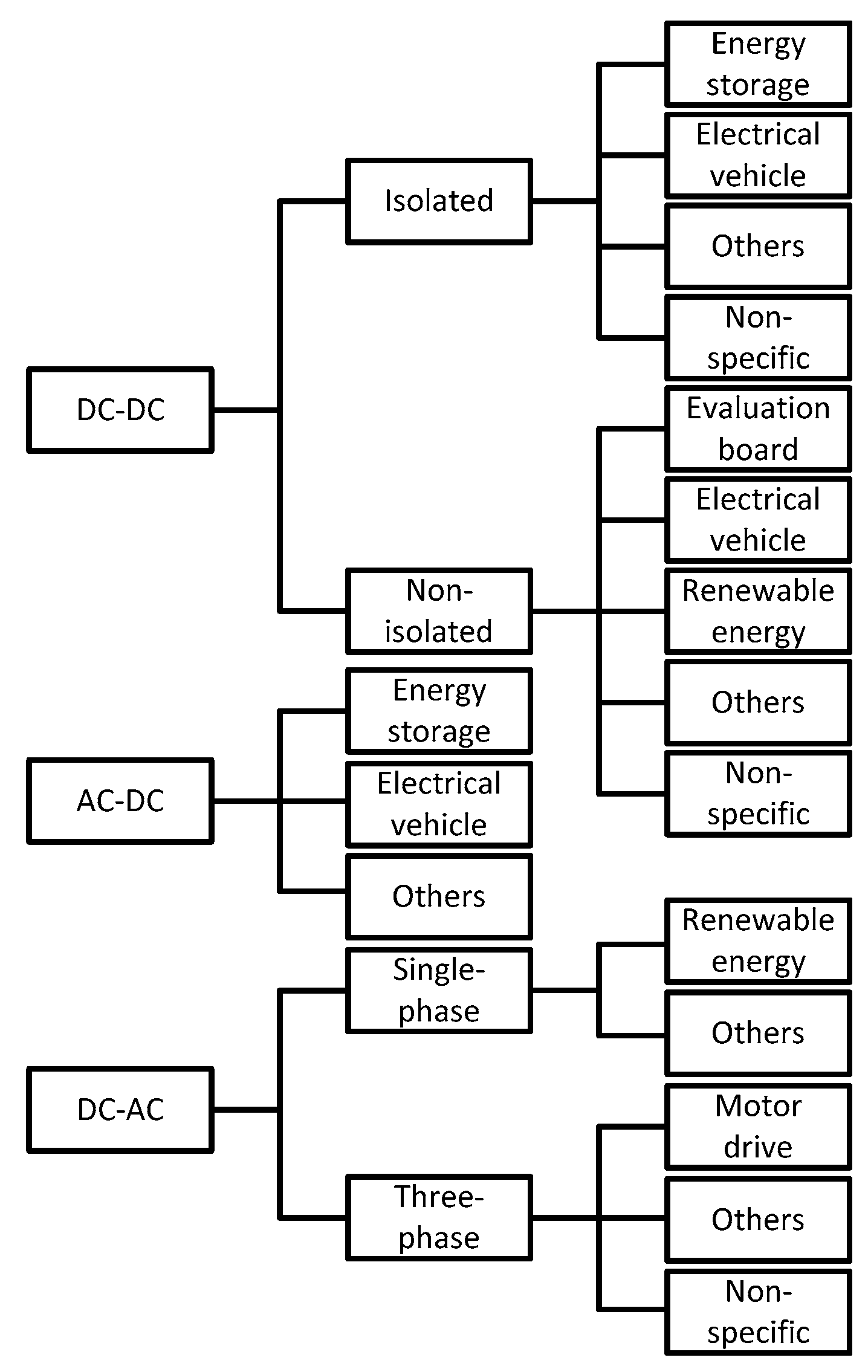
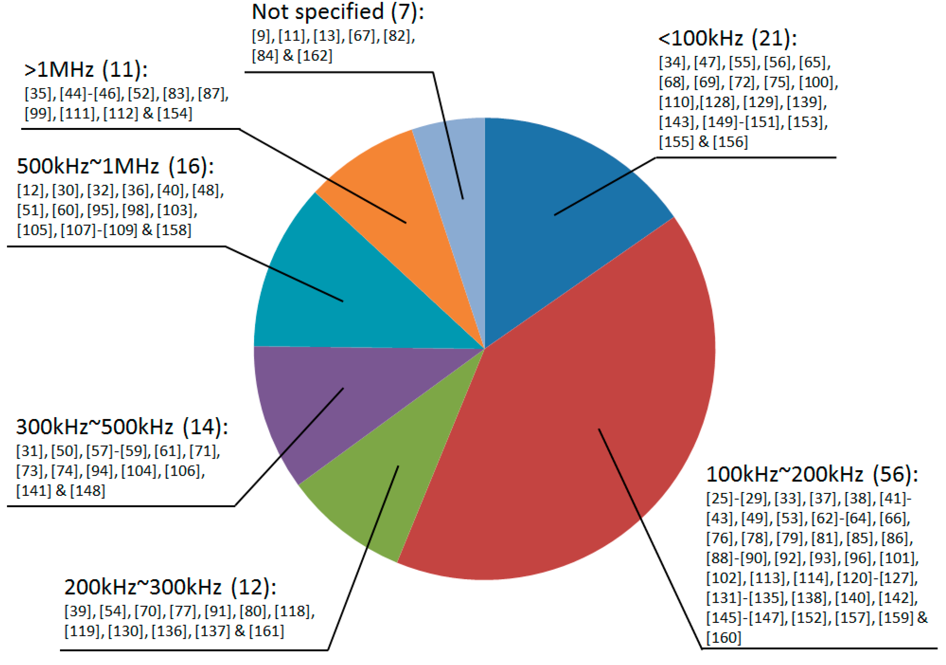
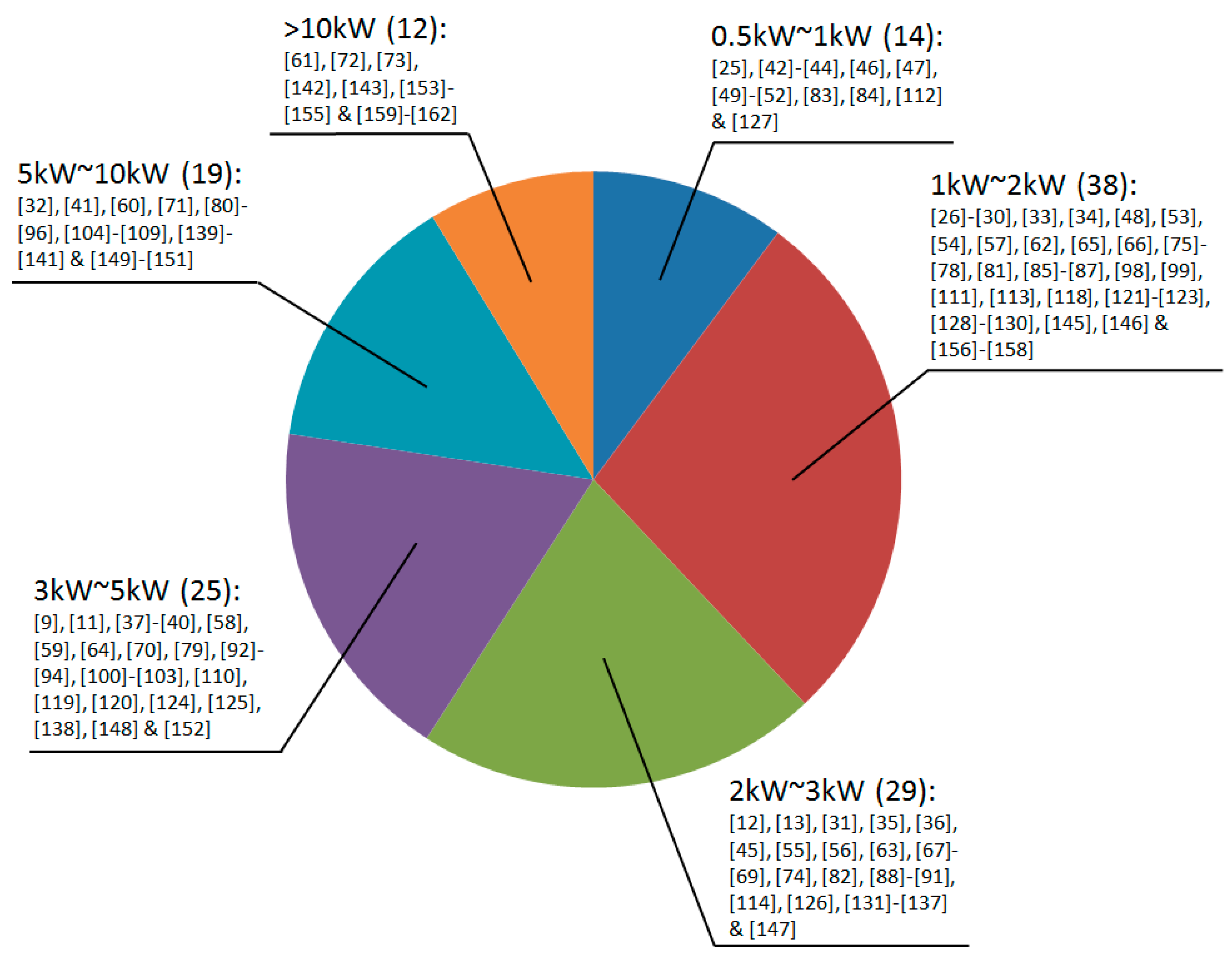
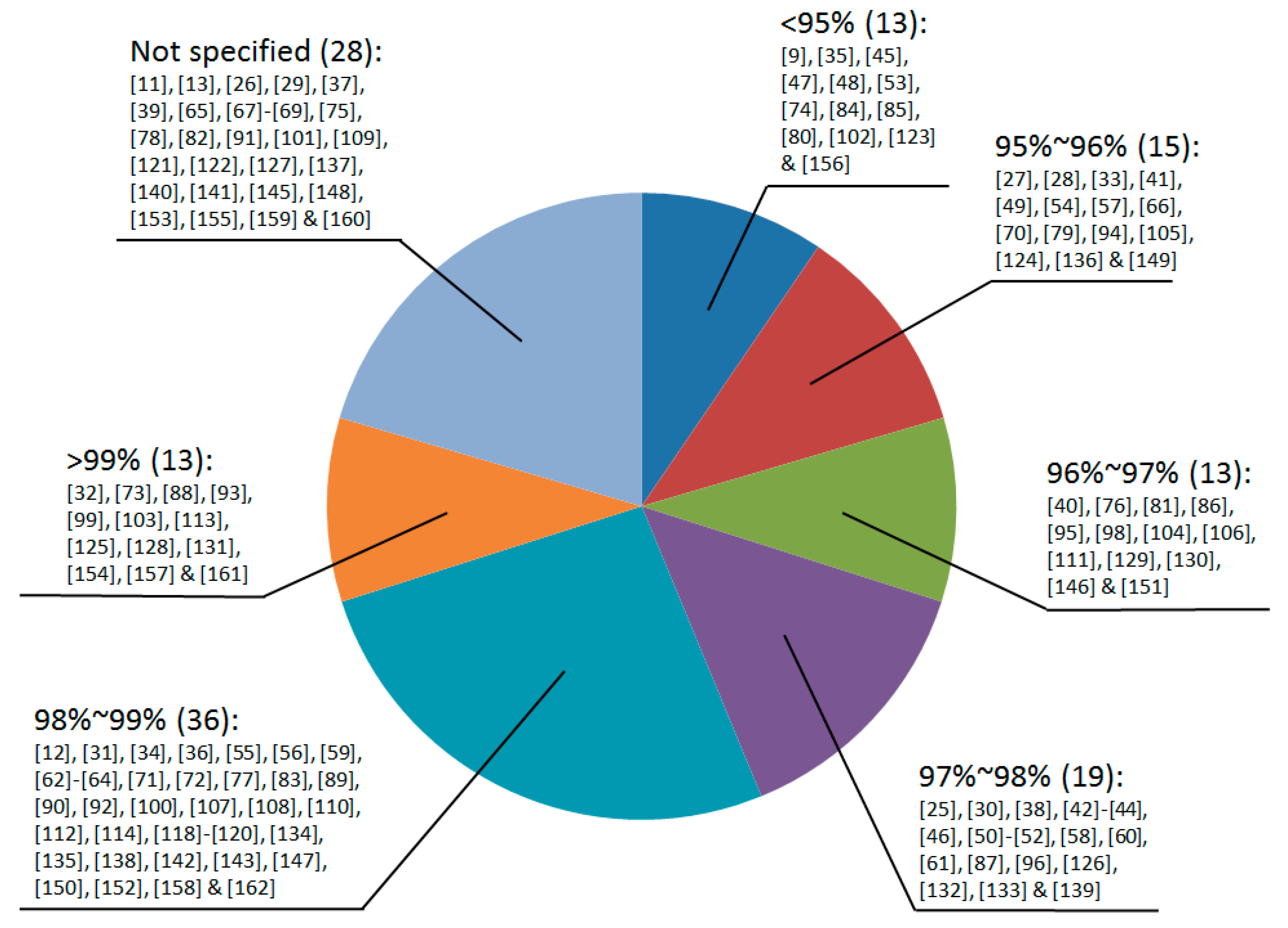
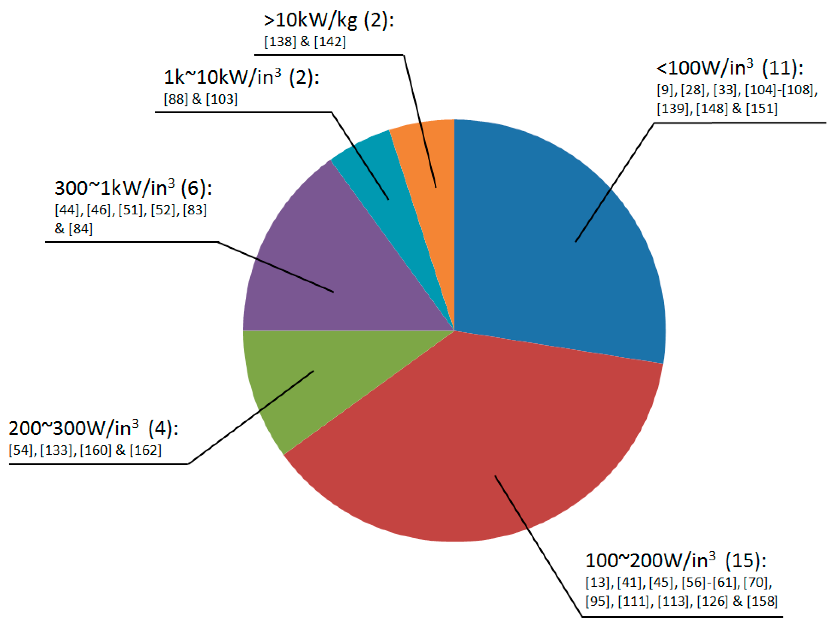
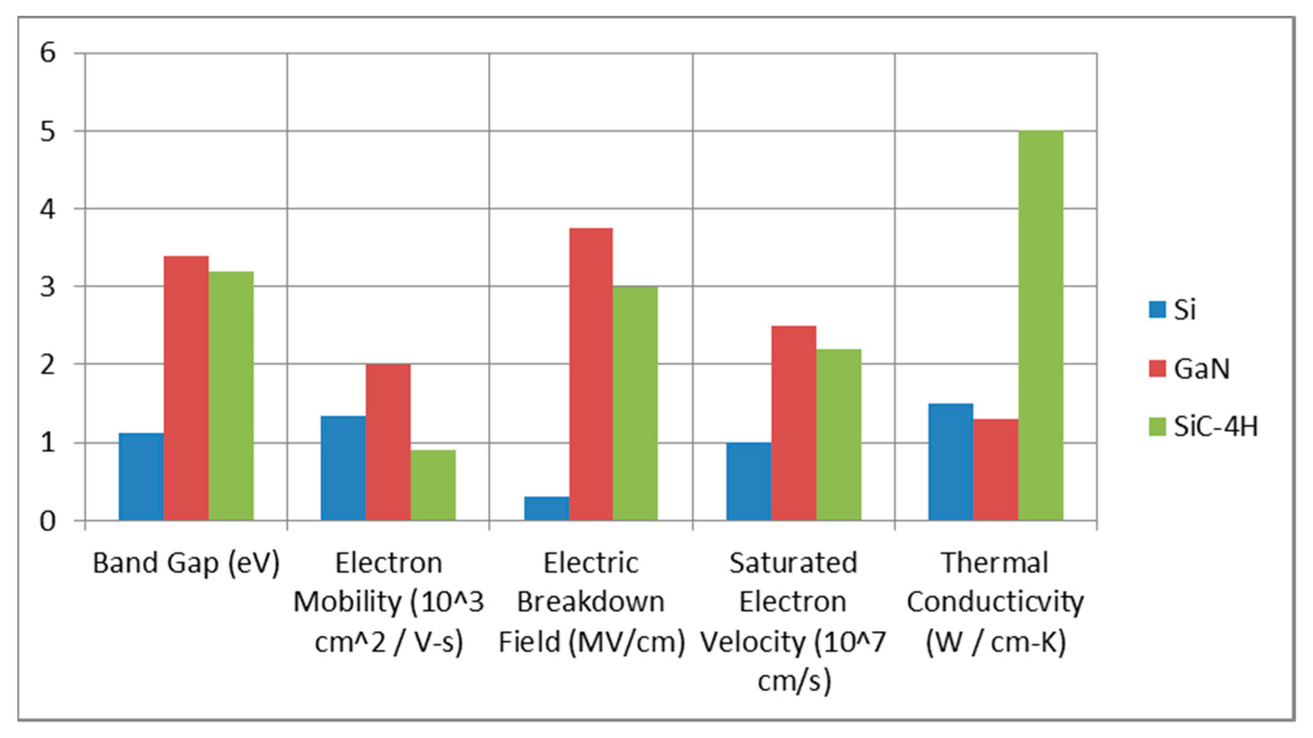
Table 1.
Reviewed papers. DC—direct current; AC—alternating current.
| Field | Amount | References |
|---|---|---|
| Isolated DC–DC converter | 38 | [9,25–61] |
| Non-isolated DC–DC converter | 36 | [11,62–96] |
| AC–DC converter | 19 | [12,13,98–114] |
| Single-phase DC–AC converter | 26 | [118–143] |
| Three-phase DC–AC converter | 18 | [145–162] |
Table 2.
Commercial gallium nitride (GaN) high-electron-mobility transistors (HEMTs) by Transphorm and GaN Systems.
Table 2.
Commercial gallium nitride (GaN) high-electron-mobility transistors (HEMTs) by Transphorm and GaN Systems.
| Manufacturer | Device | Vds (V) | Id (A) | VTH (V) | Vgs (V) | Rds(on) (mΩ) | Ciss (pF) |
|---|---|---|---|---|---|---|---|
| Transphorm | TPH3206PSB | 650 | 16 | 2.1 | ±18 | 150 | 720 |
| Transphorm | TPH3208PS | 650 | 20 | 2.1 | ±18 | 130 | 760 |
| Transphorm | TPH3212PS | 650 | 28 | 2.6 | ±18 | 72 | 1130 |
| Transphorm | TP65H050WS | 650 | 34 | 4 | ±20 | 60 | 1000 |
| Transphorm | TPH3205WSBQA | 650 | 35.2 | 2.1 | ±18 | 62 | 2200 |
| Transphorm | TPH3205WSB | 650 | 36 | 2.6 | ±18 | 63 | 2200 |
| Transphorm | TP65H035WS | 650 | 46.5 | 4 | ±20 | 35 | 1500 |
| Transphorm | TPH3207WS | 650 | 50 | 2.65 | ±18 | 41 | 2197 |
| Transphorm | TP90H180PS | 900 | 15 | 2.1 | ±18 | 205 | 780 |
| GaN Systems | GS66502B | 650 | 7.5 | 1.3 | −10 to +7 | 200 | 65 |
| GaN Systems | GS66504B | 650 | 15 | 1.3 | −10 to +7 | 100 | 130 |
| GaN Systems | GS66506T | 650 | 22 | 1.3 | −10 to +7 | 67 | 195 |
| GaN Systems | GS66508B | 650 | 30 | 1.3 | −10 to +7 | 50 | 260 |
| GaN Systems | GS66508P | 650 | 30 | 1.7 | −10 to +7 | 50 | 260 |
| GaN Systems | GS66508T | 650 | 30 | 1.7 | −10 to +7 | 50 | 260 |
| GaN Systems | GS66516B | 650 | 60 | 1.3 | −10 to +7 | 25 | 520 |
| GaN Systems | GS66516T | 650 | 60 | 1.3 | −10 to +7 | 25 | 520 |
Table 3.
Commercial GaN HEMT drivers by Texas Instruments (TI).
| Driver | Number of Channels | Peak Output Current (A) | Supply Voltage (V) | Rise Time (ns) | Fall Time (ns) | Propagation Delay (ns) |
|---|---|---|---|---|---|---|
| LMG1020 | 1 | 7 | 5 | 4 | 1.9 | 2.5 |
| LMG1205 | 2 | 5 | 4.5–5.5 | 7 | 3.5 | 35 |
| LMG1210 | 2 | 1.5 | 5 | 5.6 | 3.3 | 10 |
| LM5113-Q1 | 2 | 5 | 4.5–5.5 | 7 | 3.5 | 30 |
| UCC27611 | 1 | 6 | 4–18 | 9 | 4 | 14 |
Table 4.
Commercial GaN HEMT drivers by Silicon Lab.
| Driver | Number of Channels | Peak Output Current (A) | Input Supply Voltage (V) | Output Supply Voltage (V) | Rise Time (ns) | Fall Time (ns) | Propagation Delay (ns) |
|---|---|---|---|---|---|---|---|
| Si823x series | 2 | 0.5 or 4 | 4.5–5.5 or 2.7–5.5 | 6.5–24 | 20 or 12 | 20 or 12 | 60 |
| Si826x series | 1 | 0.6 or 4 | X | 6.5–30 | 5.5 | 8.5 | 60 |
| Si827x series | 2 | 4 | 2.5–5.5 | 4.2–30 | 10.5 | 13.3 | 60 |
| Si8220/1 | 1 | 0.5/2.5 | X | 6.5–24 | 30 or 20 | 30 or 20 | 60/40 |
| Si8239x series | 2 | 4 | 2.5–5.5 | 6.5–24 | 12 | 12 | 30 |
| Si8285/6 | 1 | 4 | 2.8–5.5 | 9.5–30 | 5.5 | 8.5 | 50 |
Table 5.
Commercial GaN switching modules by TI.
| Module | Number of Channels | Voltage and Current Ratings (V, A) | Supply Voltage (V) | Rise Time (ns) | Fall Time (ns) | Propagation Delay (ns) |
|---|---|---|---|---|---|---|
| LMG3410 | 1 | 600, 12 | 5 | 4.2 | 15 | 20 |
| LMG3410R050 | 1 | 600, 12 | 12 | 15 | 1.2 | 20 |
| LMG3410R070 & LMG3411R070 | 1 | 600, 40 | 12 | 15 | 4.2 | 20 |
| LMG5200 | 2 | 80, 10 | 5 | X | X | 29.5 |
Table 6.
Highest reported values of switching frequencies, efficiencies, and power densities in reviewed isolated DC–DC converters.
Table 6.
Highest reported values of switching frequencies, efficiencies, and power densities in reviewed isolated DC–DC converters.
| Power (kW) | Switching Frequency (Hz) | Efficiency (%) | Power Density (W/in3) |
|---|---|---|---|
| <1 | 1 M | 97.6 | 900 |
| [44,46,52] | [42,43] | [44,46,52] | |
| 1–2 | 600 k | 98.2 | 222.8 |
| [30] | [34] | [54] | |
| 2–3 | 1 M | 98.7 | 114.7 |
| [35,45] | [31] | [56] | |
| 3–4 | 500 k | 98 | 140 |
| [40] | [59] | [58,59] |
Table 7.
Highest reported values of switching frequencies, efficiencies, and power densities in reviewed non-isolated DC–DC converters.
Table 7.
Highest reported values of switching frequencies, efficiencies, and power densities in reviewed non-isolated DC–DC converters.
| Power (kW) | Switching Frequency (Hz) | Efficiency (%) | Power Density (W/in3) |
|---|---|---|---|
| <1 | 1 M | 98 | 1 k |
| [83] | [83] | [83] | |
| 1–2 | 1 M | 98.6 | Not revealed |
| [87] | [62] | ||
| 2–3 | 300 k | 98.9 | 9.5 k |
| [74] | [63] | [88] | |
| 3–4 | 200 k | 99.2 | 142.5 |
| [70] | [93] | [70] |
Table 8.
Highest reported values of switching frequencies, efficiencies, and power densities in reviewed AC–DC converters.
Table 8.
Highest reported values of switching frequencies, efficiencies, and power densities in reviewed AC–DC converters.
| Power (kW) | Switching Frequency (Hz) | Efficiency (%) | Power Density (W/in3) |
|---|---|---|---|
| <1 | 3 M | 98.6 | Not revealed |
| [112] | [112] | ||
| 1–2 | 1 M | 99.3 | 155 |
| [99,111] | [99] | [113] | |
| 2–3 | 620 k | 98.5 | 170 |
| [12] | [114] | [13] | |
| 3–4 | 500 k | 99.2 | 2.2 k |
| [103] | [103] | [103] |
Table 9.
Highest reported values of switching frequencies, efficiencies, and power densities in reviewed single-phase DC–AC converters.
Table 9.
Highest reported values of switching frequencies, efficiencies, and power densities in reviewed single-phase DC–AC converters.
| Power (kW) | Switching Frequency (Hz) | Efficiency (%) | Power Density (W/in3) |
|---|---|---|---|
| <1 | 100 k | Not revealed | Not revealed |
| [127] | |||
| 1–2 | 260 k | 99.5 | Not revealed |
| [130] | [128] | ||
| 2–3 | 250 k | 99.6 | 216 |
| [136] | [131] | [133] | |
| 3–4 | 200 k | 99 | Not revealed |
| [119] | [125] |
Table 10.
Highest reported values of switching frequencies, efficiencies, and power densities in reviewed three-phase DC–AC converters.
Table 10.
Highest reported values of switching frequencies, efficiencies, and power densities in reviewed three-phase DC–AC converters.
| Power (kW) | Switching Frequency (Hz) | Efficiency (%) | Power Density (W/in3) |
|---|---|---|---|
| 1–2 | 500 k | 99.4 | 116.3 |
| [158] | [157] | [158] | |
| 2–3 | 100 k | 98 | Not revealed |
| [147] | [147] | ||
| 3–4 | 300 k | 98.5 | 43.9 |
| [148] | [152] | [148] | |
| 10 | 13.56 M | 99.6 | 286.7 |
| [154] | [161] | [160] |
© 2019 by the authors. Licensee MDPI, Basel, Switzerland. This article is an open access article distributed under the terms and conditions of the Creative Commons Attribution (CC BY) license (http://creativecommons.org/licenses/by/4.0/).
Share and Cite
MDPI and ACS Style
Ma, C.-T.; Gu, Z.-H. Review of GaN HEMT Applications in Power Converters over 500 W. Electronics 2019, 8, 1401. https://0-doi-org.brum.beds.ac.uk/10.3390/electronics8121401
AMA Style
Ma C-T, Gu Z-H. Review of GaN HEMT Applications in Power Converters over 500 W. Electronics. 2019; 8(12):1401. https://0-doi-org.brum.beds.ac.uk/10.3390/electronics8121401
Chicago/Turabian StyleMa, Chao-Tsung, and Zhen-Huang Gu. 2019. "Review of GaN HEMT Applications in Power Converters over 500 W" Electronics 8, no. 12: 1401. https://0-doi-org.brum.beds.ac.uk/10.3390/electronics8121401
Note that from the first issue of 2016, this journal uses article numbers instead of page numbers. See further details here.