Comparison of Series Compensation Topologies for Inductive Chargers of Biomedical Implantable Devices


School of Electrical and Computer Engineers, National Technical University of Athens, 9, Iroon Polytechniou St, 15780 Zografou, Greece
*
Author to whom correspondence should be addressed.
Electronics 2020, 9(1), 8; https://0-doi-org.brum.beds.ac.uk/10.3390/electronics9010008
Submission received: 15 November 2019
/
Revised: 11 December 2019
/
Accepted: 16 December 2019
/
Published: 19 December 2019
(This article belongs to the Section Bioelectronics)
Abstract
:Modern biomedical implantable devices provide an increasingly popular solution for health monitoring and medical issues. Their level of development in the coming years will depend on their reliability and endurance. Their powering and recharging capabilities are key factors for their dominance. In this work, series compensation topologies for use in inductive chargers of biomedical implantable devices are investigated with regard to their performance. The goal is to assess the possibility of reducing the component count of the implantable device and thus, increase its reliability and patient safety. Comparison is performed between the commonly used series-series compensation topology with a topology which incorporates no capacitors in the secondary side but only series compensation in the primary. Extensive investigation of the operation of the two topologies is made through mathematical analysis, simulations, and experimental evaluation, for the most popular schemes of operation, with regard to frequency selection. A prototype inductive charger, including a custom-made inductive link, was designed and built for the experimental evaluation of the system. Insights on the operation of both topologies are provided and the results show that primary-side series compensation can be a strong alternative to series-series compensation, in biomedical applications.
1. Introduction
Modern medicine is increasingly making use of biomedical implantable devices to deal with common medical conditions and to enhance the monitoring of patients’ health [1]. Pacemakers [2], defibrillators, left ventricular assist devices [3,4], neuro-stimulators, cochlear implants [5], and infusion pumps [6] are some of the most well-known applications of such systems, but research is ongoing for the expansion of the use of implantable devices in more medical fields.
The common characteristic of these systems is that they are powered by batteries, which ultimately determine their lifetime and performance potentials. In order for these devices to be implantable, they have to take up as small a space inside the human body as possible. More importantly, they would ideally have to last for a lifetime, in order to avoid repetitive operations for surgical removal and reimplantation, which increase the risk for infections. One approach to serve both goals is the solution of incorporating a low capacity-small volume battery in combination with a wireless recharging system. Adding a recharging system does in fact increase the overall volume of the implant but provides significant benefits with regard to battery minimization and avoidance of extra surgeries in the long run. The recharging option allows for an increased exploitation of the capabilities of implantable devices, as energy consumption is no longer a restricting factor. Full use of such devices can translate to more detailed and frequent health monitoring schemes, extra activities, and even real-time communication of health data to the patient and their doctors. This is the reason why the research community is focusing on the development of robust and versatile wireless charging equipment for medical implantable devices [6,7].
Wireless charging can be performed via inductive coupling or by transferring power at frequencies in the MHz [8] and GHz range. The latter is associated with a higher impact on human tissues [9,10,11,12,13] compared to the former and, for this reason, it is preferred for deeply implanted [14,15] or millimeter-sized [16] medical devices, which charge at a very low power. Inductive charging is more attractive for medium to higher power transfer, but also suitable for low power systems [17]. It is selected for medical applications which require charging in the range of a few W, such as pacemakers. Inductive power transfer is achieved when a primary coil, attached to an external charger, transmits power to a receiving coil, which is implanted together with the medical device inside the patient’s body. This contactless energy transfer technique allows for the recharging of the battery of the implanted device, without removing the device from the patient, or having driveline cords passing through the patient’s skin to connect the implant with an external powering system.
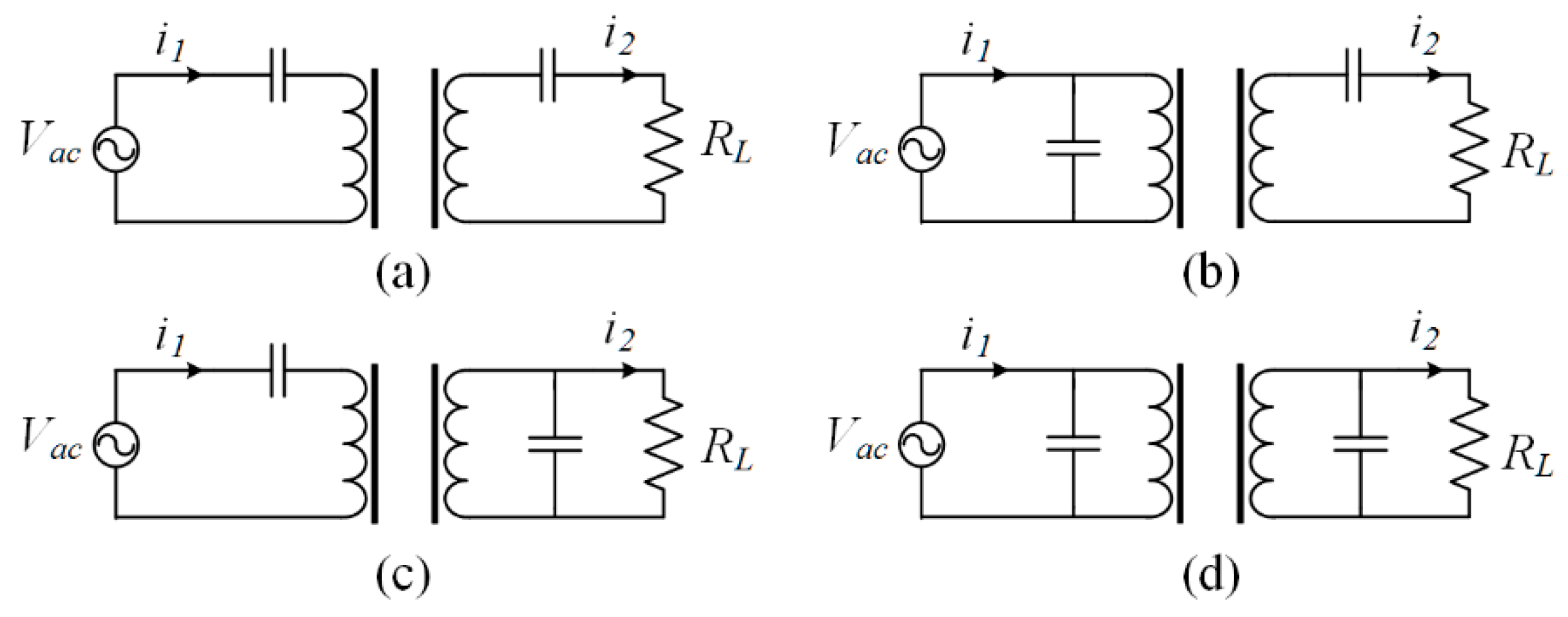
In inductive power transfer systems (IPTSs) capacitors are incorporated to compensate for the significant leakage inductances caused by the weak coupling between the transmitter and receiver coils. In most IPTSs compensation is used in both sides of the system. When operating at resonant conditions, significant power transfer can be achieved. The typical compensation topologies are illustrated in Figure 1.
The compensation topology is chosen taking into account the specific requirements of each application. Series compensation is selected for operation at higher voltages and lower currents, which leads to high efficiency of the inductive charger. On the other hand, parallel compensation behaves as a current source and can achieve power transfer at lower coupling conditions or operating frequency, due to the larger current in the resonant loop. However, due to the latter, operation at lower efficiency is obtained [18]. For these reasons, the series-series topology is more commonly selected for wireless charging systems.
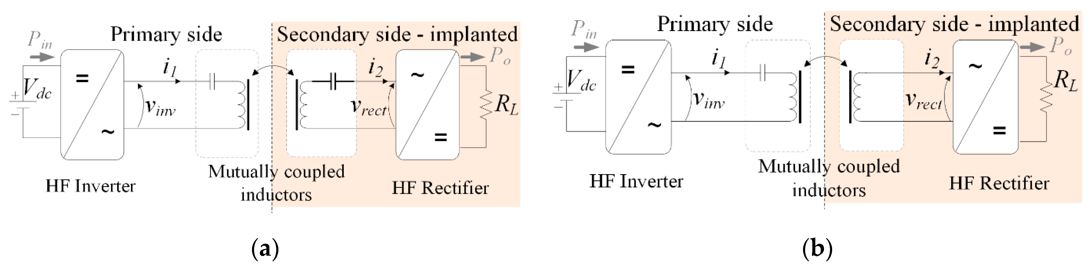
Specifically, for implant applications, size and reliability matter the most. Inevitably, any component added to the implantable part of the wireless charger has a negative effect on both its size and its lifetime. Thus, it is worth investigating the options for developing a contactless charger with the minimum component count in the implantable side of the system. With respect to the inductive link of the wireless charger, component minimization can be achieved by removing the compensating capacitor from the secondary, implantable side of the system. The elimination of the compensating capacitor decreases by one component the total count of the secondary-implantable side of the charger, which includes another six elements: the coil, four diodes of the rectifier, and the capacitor acting as an output filter. This improves the lifetime of the implantable system and slightly decreases its volume. Additionally, the operation of the secondary side without a resonant circuit leads to the limitation of the exposure of human tissue to large differential voltages that appear across the resonant circuit components during operation at resonant conditions.
To this end, in this work, investigation of the topology depicted in Figure 2b, employing a single capacitor only in the primary side of the inductive charger is performed and comparison is made with the typical series-series compensation topology, presented in Figure 2a. Despite the fact that all topologies depicted in Figure 1 have been thoroughly investigated in literature, for an extensive range of applications and conditions of operation, limited analysis has been published regarding single-side compensation for IPTSs. In fact, wireless power transfer systems employing a single compensation have been proposed and elaborated in [19] and [20], but, in these cases, the compensating capacitor was placed at the secondary side. Additionally, analysis of a wide range of compensation topologies is presented in [21]. To the best of the authors’ knowledge, there is no extensive investigation of the operation features of the topology incorporating compensation only in the primary side for inductive power transfer applications.
In this work, theoretical analysis for various conditions of operation is presented for both the series-series and the primary side series compensation topologies, for various conditions of operation, which is presented in Section 2. Discussion on the common schemes for frequency selection is included in Section 3. The design, construction, and evaluation through three-dimensional (3D) simulations and experiments of the inductive link of the contactless charger is reported in Section 4. Evaluation and comparison between the two systems is completed in Section 4, through simulations and experiments on a custom-made 2W prototype inductive charger.
2. Analysis of Series-Compensation Topologies
In this section, mathematical analysis of the investigated systems is performed by first harmonic approximation, under the assumption that power transfer is achieved through the fundamental frequency of operation, since the systems operate in conditions of resonance.
2.1. Series-Series Compensated IPTS
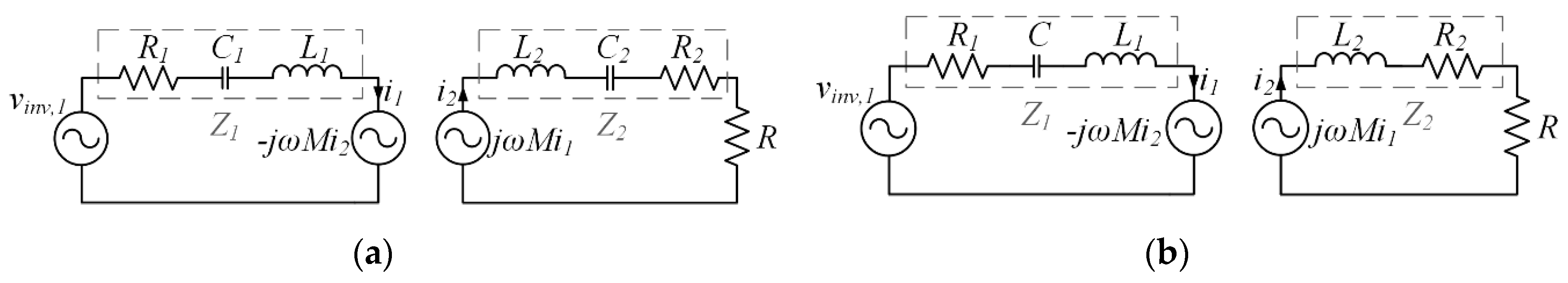
The equivalent circuit of the series-series (SS) compensated IPTS is depicted in Figure 3a. C1 and C2 represent the compensating capacitors of the primary and secondary side of the system, respectively. Likewise, L1 and L2 are the primary and secondary coil inductances. M is the mutual inductance, is the coupling coefficient, R1 and R2 are the internal resistances of the resonant circuits, R is the reflected load to the ac side of the secondary system, and vinv,1 is the first harmonic of the inverter output voltage.
The equivalent resistance of the battery, R, as reflected to the source via a full wave rectifier with a capacitive output filter, is obtained by Equation (1) and is proportional to the ratio of the battery voltage over the charging current. That is the value that represents the loading effect of the battery on the power supply. According to Knecht et al. [3], this simple equivalent of the load resistance reflection to the source is fairly accurate, as it provides almost identical results with other extended load models.
The primary and secondary side impedances, Z1 and Z2, are given by Equations (2) and (3), respectively. By analyzing the equivalent circuit, the system voltage gain is calculated by Equation (4), which results in Equation (5).
If, for simplification, the internal resistances are considered negligible, R1 = R2 = 0, the coupled coils are designed to be identical, L1 = L2 = L, and C1 = C2 = C the voltage gain is provided by Equation (6).
As can be seen, the output voltage depends on both the load value and the coupling coefficient of the coils. In other words, even if the frequency is appropriately selected for a specific set of values of inductances (L) and compensating capacitances (C), as well as a specific position of the coils, which translates to a constant coupling coefficient, then a given M, the voltage gain, vo/vinv,1, will still change as the battery state of charge (RL) changes.
For operation at the natural frequency of the primary side, , the voltage gain is
For operation at the frequency for which the imaginary part of Equation (6) is zero, that is for
the voltage gain is equal to 1, as explained in [22]. It is worth mentioning that ωr is the frequency for which, as can be obtained by Equation (6), the output current, i2, is in phase with the input voltage, vinv,1.
For this topology, the unity input power factor is achieved at three frequencies, the natural frequency, ωn, ωPFH, and ωPFL. The latter are provided by Equation (9). At ωn, as explained above, the voltage gain is given by Equation (7), whereas, at both ωPFH and ωPFL, the voltage gain is dependent on both the coupling coefficient and the load value, as expressed by Equation (10).
2.2. Primary-Side Series Compensated IPTS
In the second topology, illustrated in Figure 3b, the difference with the series-series compensated topology is the use of a single compensating capacitor, C, in the primary side of the system and no compensation in the secondary side. Thus, the secondary side impedance is given by Equation (11). Following the same procedure for the analysis of the primary-side series (PSS) compensated IPTS, yields Equations (12) and (13).
Applying the same simplification hypothesis as before (i.e., the internal resistances are considered negligible, R1 = R2 = 0, and the coupled coils are designed to be identical, L1 = L2 = L) the voltage gain takes the form of Equation (14), which, for operation at the natural frequency of the primary side, , leads to Equation (15). The most interesting result is that the voltage gain is the same as in the case of the series-series compensation.
For operation at the frequency for which the imaginary part of Equation (12) is zero, that is for
the voltage gain becomes
which means that the output voltage depends only on the coupling coefficient of the coils. Additionally, since k < 0.6 in these loosely coupled systems, the voltage gain is always greater than 1.67. ωr is, for this case too, the frequency for which the output current, i2, is in phase with the input voltage, vinv,1, as can be derived by Equation (13).
Unity input power factor is achieved when the inverter output voltage and the primary current are in phase. According to Equations (18)–(20), the necessary condition is that Im{vinv,1/i1} = 0.
This results in a single real solution, equal to
If, for simplification, the internal resistances are considered negligible, and the coupled coils are identical, the frequency of operation for unity power factor is equal to
It is evident that the optimal frequency of operation for unity power factor depends on the value of the load. For operation at ωPF, the voltage gain is
3. Discussion on the Frequency of Operation
For the selection of the frequency of operation of inductive chargers, there are three options commonly presented in literature; the most common one, which requires no adaptation to changing conditions of the load or the coupling, establishes operation at the natural frequency of the resonant circuits, ωn. Another option is the continuous adaptation of the frequency of operation of the charger to any changes in the coupling or the load. This is commonly performed in literature in two ways, both implemented with phase-locked-loop techniques, which are based on the zeroing of the phase difference between the inverter output voltage and the secondary side current (ωr) or the primary current (ωPF).
Comparisons between the two topologies analyzed in Section 2.1 and Section 2.2, with regard to the possible frequencies of operation, are made via the simplified mathematical expressions which are based on the assumption that internal resistances of the systems are negligible and identical inductances and capacitances are used, when applicable, in both sides of the systems. This hypothesis is made for the simplification of the comparison due to the highly complex mathematical relations that describe the operation of such systems. Taking the above into account, the following conclusions can be drawn.
3.1. Operation at the Natural Frequency ωn
For operation at the natural frequency ωn, the output voltage gain is the same for both topologies and equal to Equation (7). This means that for the said frequency of operation the primary-side series compensated topology is an equal substitute for the series-series compensated topology.
Due to the fact that at ωn the output voltage depends on the coupling coefficient and the value of the load, adoption of an output power control technique may be necessary. Using a DC/DC converter or an inverter phase-shift technique [23] to properly adjust input voltage can be a suitable output power control strategy.
3.2. Operation at ωr
ωr is the frequency for which, in both topologies, the output current, i2, is in phase with the input voltage, vinv,1. The voltage gain for the PSS topology is provided by Equation (17), whereas for the SS topology is unity. Therefore, a difference between the two topologies exists in this case.
For the PSS topology dependence on the coupling coefficient is observed, that is, the positioning of the coupled coils will affect the output voltage of the system. This is not the case for the SS topology, for which operation at ωr essentially ensures constant output voltage. While this advantage of the SS topology may initially seem like a legitimate reason for selecting the latter over the PSS topology, one has to consider the requirements for achieving and maintaining the desired frequency of operation.
Since zeroing the phase difference between i2 and vinv,1 is the criterion for tracking ωr, real-time sensing of the zero-crossing of the secondary side is necessary. This can be performed only in the secondary side and has to be transmitted to the primary side at real-time and ideally without any delay in the signal, so as to be compared with the inverter output voltage. Using this data, the inverter switching frequency can be adjusted accordingly so as to nullify the phase difference, with the implementation of a Phase-Locked-Loop (PLL) technique, as suggested in [22].
It is readily apparent that variable frequency control via communication with the secondary side of the system increases the complexity and component count on the secondary side sub-system and, thus, it may be more suitable for higher power implant [4] or other wireless charging applications [24]. This opposes the premise of this work, as expressed in Section 1, which promotes simple, robust secondary-side circuits, for increasing the reliability of the charger.
3.3. Operation at ωPF
Unity input power factor minimizes switching losses of the inverter in the primary side of the system, thus contributing to the increase of the system efficiency. Since the coupled coils are excited by square-wave voltage, zero current switching [25] can be achieved for operation at ωPF, where the primary side current, i1, is in phase with the input voltage, vinv,1.
The voltage gain for operation at this frequency is given by Equation (23) for the PSS topology and by Equations (7) and (10) for the SS topology. In both cases, the voltage gain depends on the coupling coefficient and the value of the load. The basic difference between the two topologies is the fact that for the SS topology, as explained in Section 2.1, there are up to three different frequencies, including the natural frequency ωn, for which the phase difference between i1 and vinv,1 is zero. This phenomenon is known as bifurcation [26] and has been reported to cause difficulties in frequency tracking and control techniques [27]. On the contrary, for the PSS topology the said phase difference becomes zero for a single frequency given by Equation (22).
In either topology, for this case PLL control strategies can be used, in order to track and maintain the desired frequency of operation. Since all the necessary sensors and circuitry are located in the primary side of the system, this sophisticated control does not burden the secondary sub-system.
4. Design and Evaluation of the Inductive Link
Most inductive chargers for biomedical implants incorporate planar circular or spiral coils [4,17,28,29] due to the space restrictions applying to the implantable coil. Optimal operation is achieved when the primary coil is perfectly aligned with the secondary coil. In such cases, the air gap ranges from 3 to 4 mm, which accounts for a typical skin depth [9,10,30].
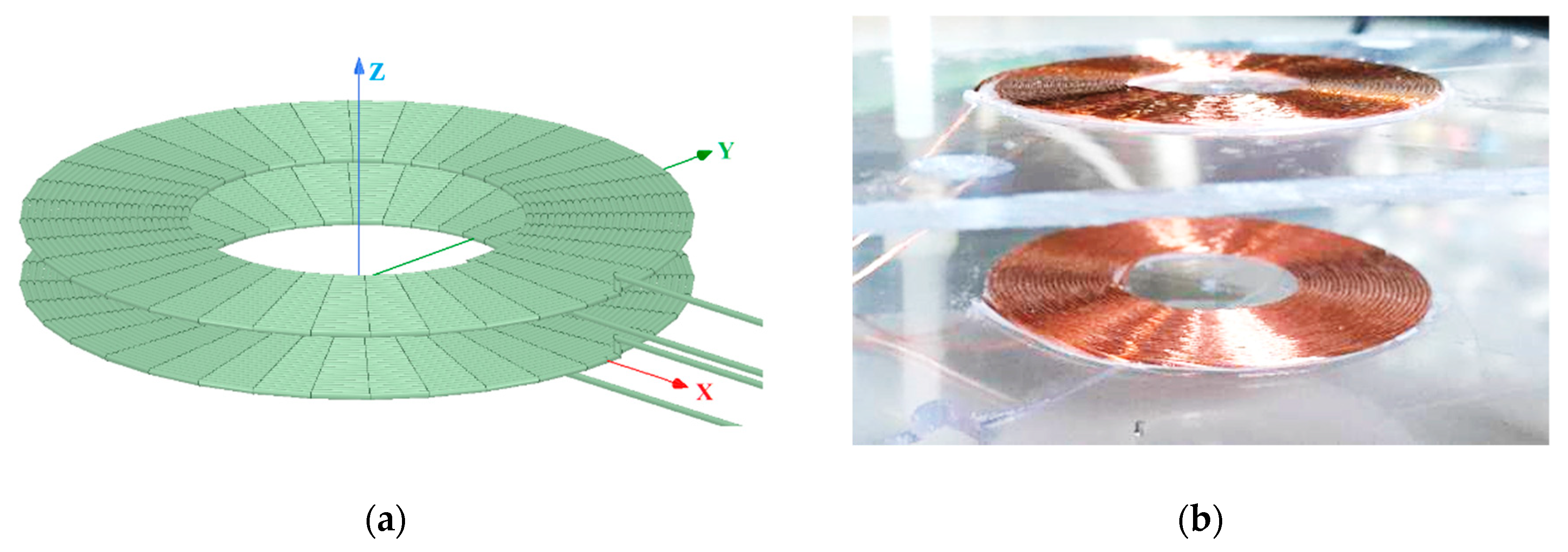
For the evaluation of the coupling coefficient for various positions of the charger, simulations are performed with the 3D finite element method software ANSYS Maxwell for the topology depicted in Figure 4a.
Each winding has 23 turns of litz wire, consisting of 24 strands of 0.08 mm copper wire, with a total wire diameter of 0.5 mm. The total surface diameter of each coil is 45 mm, which is within the permitted range for implants [3]. Simulations for various displacement conditions are carried out. Gap lengths in the z-axis range from 3 mm to 20 mm and in the x-axis from 0 mm (perfect alignment) to 15 mm. Simulations are carried out with free air as the medium.
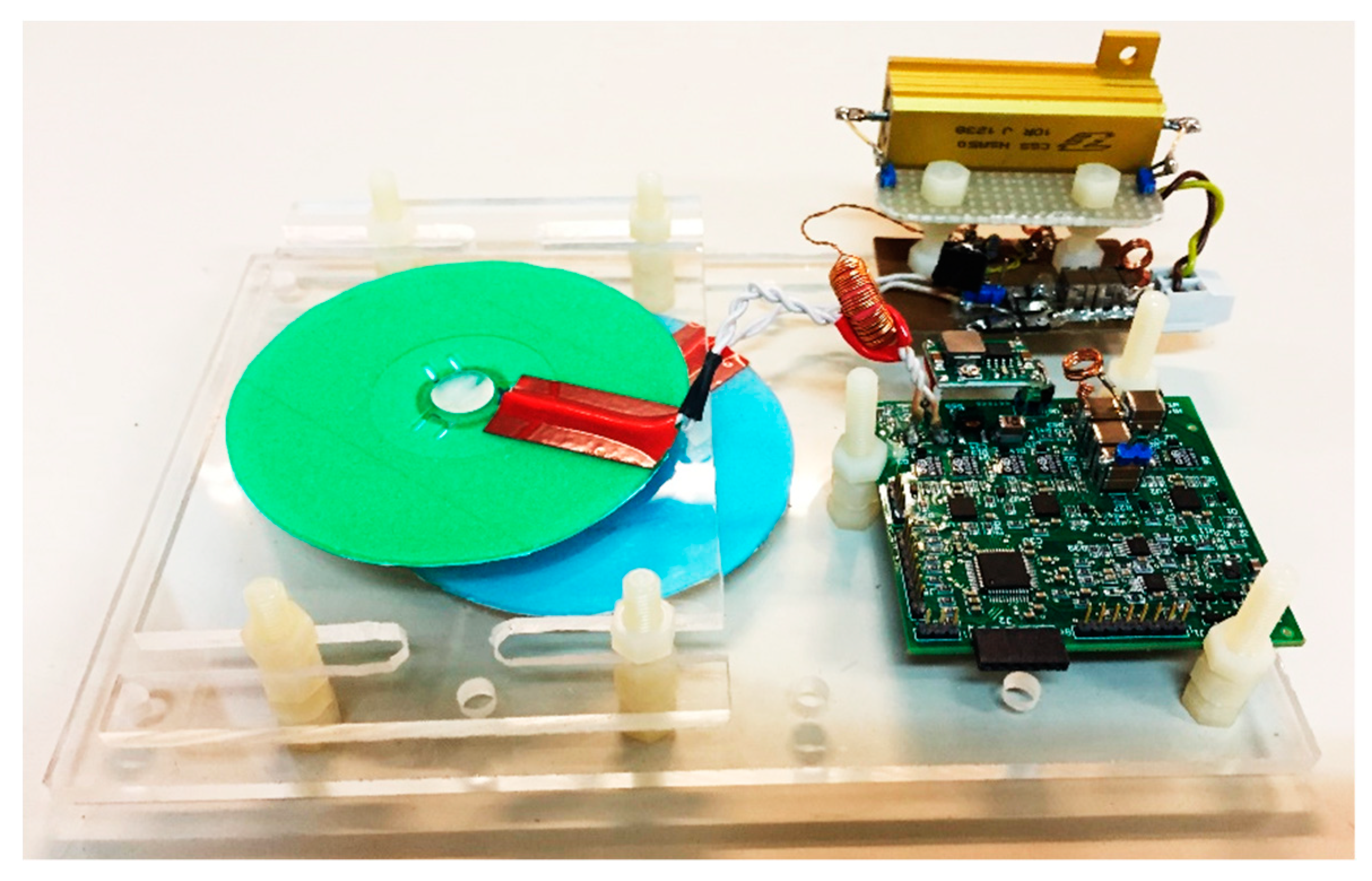
For the experimental validation of the simulation results a prototype set of coils has been constructed, with the same specifications described in the above, as illustrated in Figure 4b. The magnetic circuit is held together by a plexiglass, plastic construction which allows for relative position adjustments between the primary and secondary coils, without interfering with the magnetic flow.
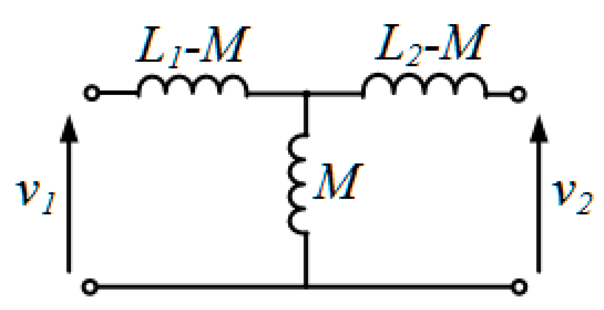
The coupling coefficient for various air gaps is experimentally measured with the voltage ratio method as follows: the open-circuit voltage of each coil is measured when the other coil is excited by a high frequency alternating voltage source, Vexc. The equivalent circuit of the coupled coils is presented in Figure 5. Based on this circuit, k is obtained by the calculations provided in Equation (24), where subscripts 1 and 2 refer to the primary and secondary coil respectively, oc denotes an open-circuited coil, while exc denotes the excited coil. L symbolizes the self-inductance and M the mutual inductance of the coils.
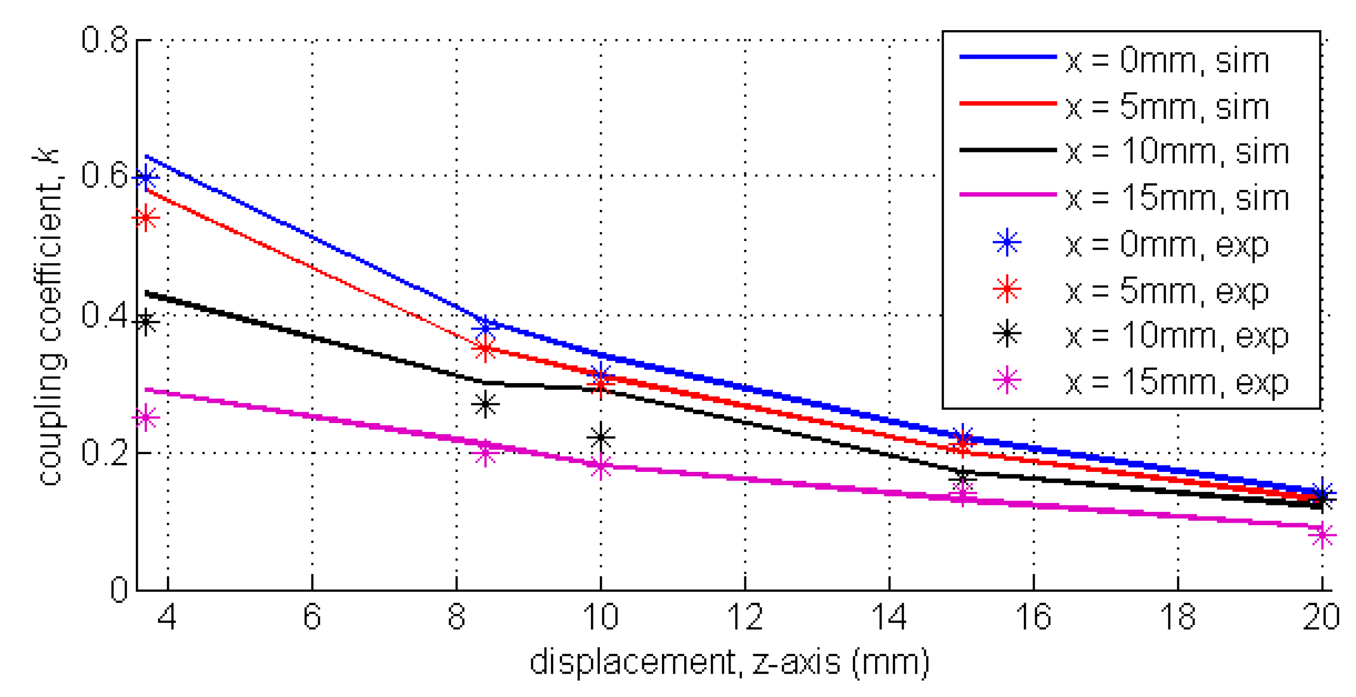
The coupling coefficient obtained by the simulations at each position is presented in Figure 6. As can be seen, k reaches 0.63 at the nominal position of the IPTS and may be reduced to 0.09 for the highest misaligned position testes, that is for x = 15 mm and z = 20 mm. In the same figure, the experimentally measured coupling coefficient for each position is marked by a discrete dot. The experimental results are very close to the simulation results. However, it must be noted that due to the small size of the coils, even the slightest displacement from the desired position leads to a significant change in the coupling. This factor may have contributed to the slight differentiation between the simulation and the experimental results.
5. Evaluation of the Inductive Charger Operation
For verification of the theoretical analysis presented in the previous sections, simulations of the topologies under investigation are performed for operation at the aforementioned frequencies and coupling conditions. Additionally, a prototype inductive charger is designed and built for the experimental evaluation of the operation of the system. Simulations and experiments are carried out for a range of resistive loads, which emulate specific states-of-charge of the battery, as explained by Equation (1). In this way, fair comparison between the two compensation topologies can be performed, as they are tested under the very same conditions. Additionally, analytical investigation and assessment of the behavior of each topology can be carried out for the different stages of the charging procedure and useful conclusions can be drawn. The respective assessment is recorded in the following subsections.
5.1. Simulation of the Inductive Charger
The electric circuits of the SS and the PSS topologies, illustrated in Figure 2a,b, are simulated using the MATLAB/Simulink platform. A full bridge inverter is used in the primary side so as to allow for controllable operation at various frequencies. A conventional full-wave rectifier is used in the secondary side of the system. The values presented in Table 1 are used for the simulations. A 0.5 Ω internal resistance is included in each side of the system in order to record a more realistic behavior. The inductance values were obtained by the magnetic circuit assessment, presented in Section 4. The capacitance values are selected so that the natural frequency of the resonant L-C circuits, fn, is 200 kHz.
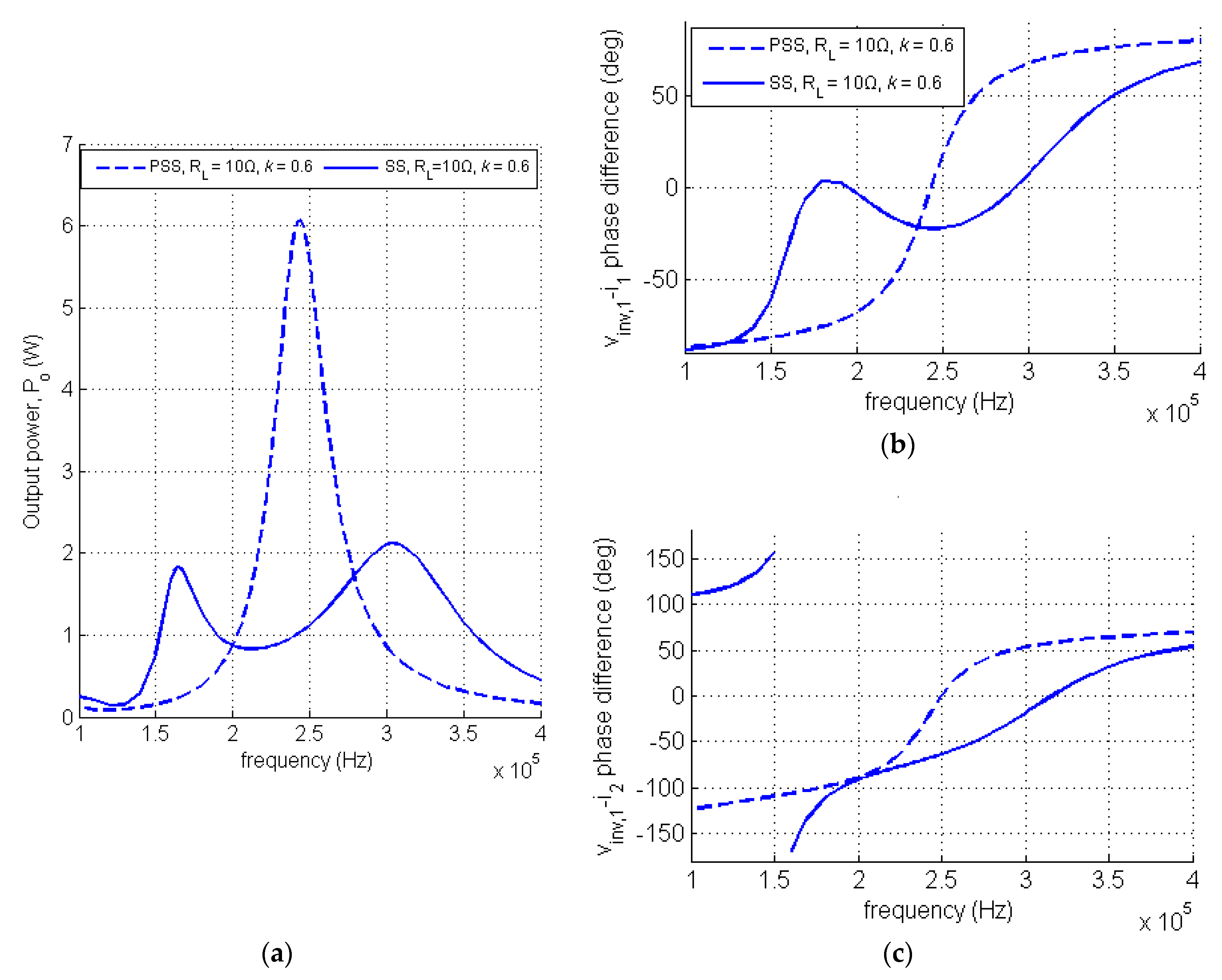
Initially, simulations are carried out for the two topologies under investigation for the whole range of frequencies. For the said simulations, RL = 12 Ω and k = 0.6. In Figure 7a, the output power is recorded. It can be seen that due to the existence of one capacitor, the PSS topology presents a single peak, whereas, the SS topology has two power peaks, due to the coexistence of two resonant circuits. In the same figure, the phase difference between the inverter output voltage and the primary current is presented. From this graph, the existence of the bifurcation phenomenon, mentioned in Section 3.3, is evident, since three frequencies for which the phase difference is zeroed are recorded for the SS topology. On the contrary, there is only one zero-phase frequency for the PSS topology. For the full presentation of the system behavior, the phase difference between the inverter output voltage and the secondary side current is also depicted in Figure 7c. In this plot, one can observe the single zero-phase frequency, which is different for each topology.
Taking into consideration the above, simulations for various conditions of coupling, as obtained by the respective investigation, are carried out in the following subsections. Load variation is performed in order to assess the operation of the charger for different states of charge of the battery.
5.1.1. Operation at the Natural Frequency ωn
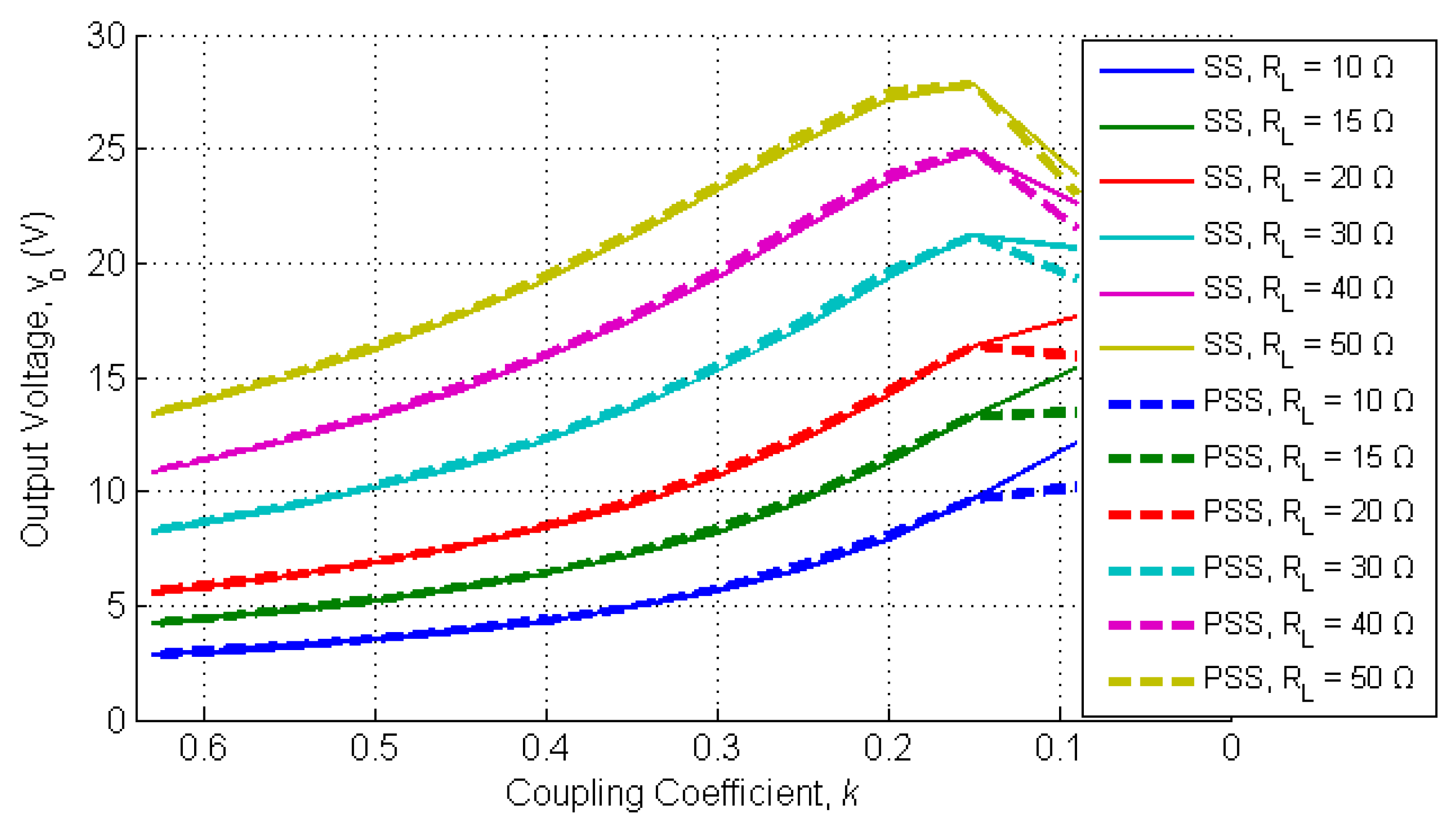
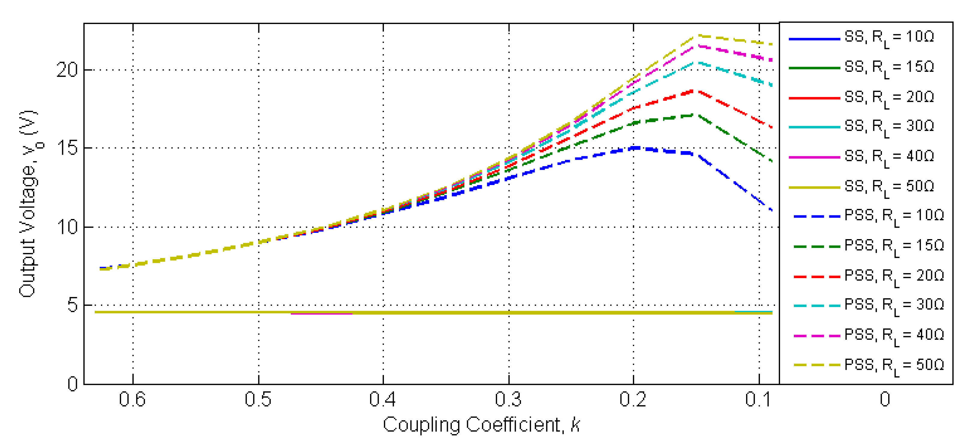
Figure 8 depicts the output voltage with respect to the coupling coefficient for various load values for the SS and the PSS topologies. As can be seen, despite the inclusion of internal resistances, the results are almost identical for both topologies for coupling coefficients ranging between 0.63 and 0.15. A small deviation is observed for the weakest coupling (k = 0.09). Simulation results are in accordance with the theoretical analysis performed in Section 2.
5.1.2. Operation at ωr
Figure 9 illustrates the output voltage with respect to the coupling coefficient for various load values for the SS and the PSS topologies, for operation at ωr. As explained in the mathematical analysis in Section 2.1, the voltage gain for the series-series compensation topology at the said frequency is equal to 1. Thus, the output voltage is equal to the input voltage, independently of the load values or coupling coefficient conditions. This is evident from the Vo = 5 V lines of the graph, which are almost steady, despite the inclusion of small internal resistances in the simulations.
On the other hand, the output voltage of the PSS topology is dependent on the coupling values, in accordance with the respective analysis in Section 2.2. It is worth noticing that for relatively strong coupling (i.e., k > 0.38) and despite the non-ideal conditions (existence of internal resistances) the voltage gain is independent of the load values and inversely proportional to k, as expressed by Equation (17). However, as the coupling weakens, it appears that the effect of the load values on the output voltage is no longer non-negligible, due to the inclusion of internal resistances.
The calculated frequencies of operation, based on Equations (8) and (16), for which simulations where carried out as listed in Table 2.
5.1.3. Operation at ωPF
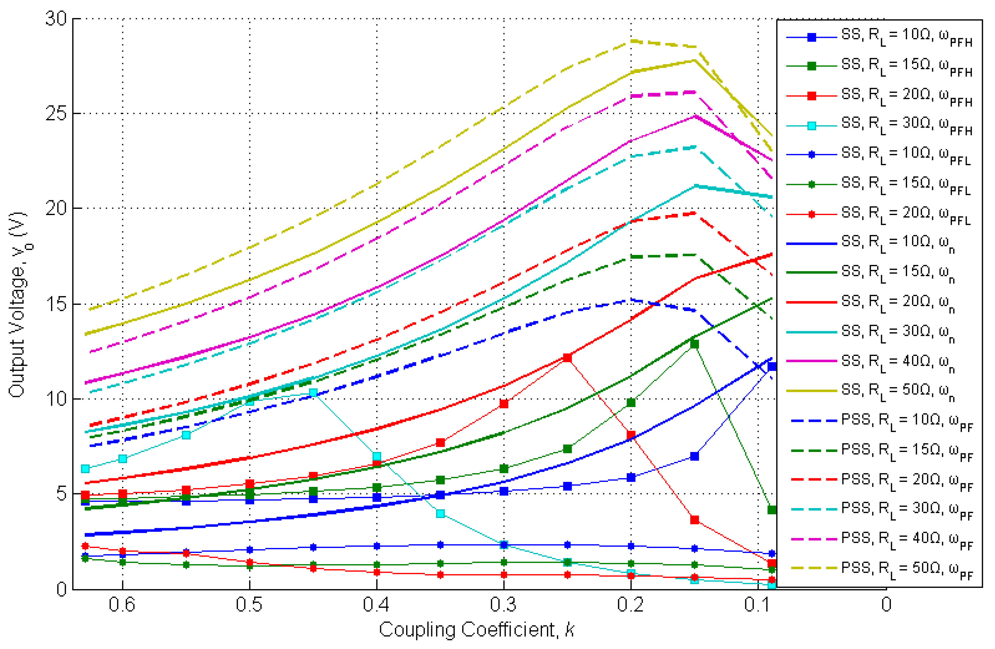
Figure 10 depicts the output voltage with respect to the coupling coefficient for various load values for the SS and PSS topologies. Operation is simulated at ωPF for the PSS topology and at ωn, ωPFH, and ωPFL for the SS topology, due to the bifurcation phenomenon. As explained in the mathematical analysis in Section 2, the voltage gain for both topologies at these frequencies of operation is dependent on the coupling and load values. It must be mentioned that for ωPFH and ωPFL simulations were performed only for the resistance loads for which there existed solutions of Equation (8) for the whole range of coupling coefficients. As can be seen, the power transfer at ωPFL is very weak and not strongly affected by the coupling.
5.2. Experimental Verification
The performance of the examined series compensation topologies was experimentally evaluated through the test-setup presented in Figure 11. The primary side full bridge inverter was constructed with four enhancement mode GaN-on-silicon power transistors (GS61004B) that exhibit low on-state resistance (RDS-on = 15 mΩ) and low input charge (QG = 6.2 nC), and favorable characteristics for high efficiency at high switching frequencies. Each GaN transistor was accompanied by an antiparallel Si Schottky barrier diode (PMEG6010) to further minimize the reverse conduction losses during the dead-time period, set to 30 ns. The power devices were driven by the LM5113-Q1 gate driver and 6V zener diodes were placed across the gate and source terminals to protect the devices from voltage overshoots. The recorded rise time was 10 ns and the respective fall time was 13 ns.
The secondary side rectifier consists of four ultra-low forward voltage drop Schottky rectifier diodes (FSV15100V) in a full bridge configuration. For ease of identification and protection, the coils of Figure 4b were encapsulated in colored plexiglass pads: green color was used for the primary side coil and blue for the secondary side coil.
High-frequency current transformers were designed to accurately capture the primary and secondary side currents, while a differential probe was used to measure the primary-side voltage. The primary and secondary compensation capacitors were selected at 33 nF. Two resistive loads (10 Ω and 20 Ω) were used for the experiments.
Taking into consideration the simulation results, according to which operation at the higher end of the coupling range is beneficial for the limitation of the output voltage, the selected area of operation of the experimental setup is k > 0.4. Due to the nature of this application, it is relatively easy to achieve good alignment and low gap between the coils, since the secondary coil is implanted right under the skin. Thus, based on the results presented in Figure 6, operation at a coupling k > 0.4 is easily achieved.
Experiments are carried out for all the examined frequencies of operation, where available. The experimental results for the SS topology are listed in Table 6 and the results for the PSS topology are in Table 7, respectively.
As can be seen, the zero-phase frequencies, ωr and ωPFH, are relatively different from the theoretically calculated ones. This is attributed to the slightly different values of the commercially available compensating capacitors (33 nF instead of the theoretically selected 30 nF), as well as the fact that in the theoretical estimation the internal resistances of the components were not taken into consideration. For the experiments, the zero-phase frequencies were selected by experimentally achieving zero phase between the inverter output voltage and the respective currents.
It must be noted that it was not possible to locate ωPFL either due to the unsuitable waveform of the primary-side current (very low current with high harmonic content) or due the fact that ωPFL was extremely close to ωn, for which case experiments had already been carried out. For a better understanding of this issue, one can refer to Figure 7b, where the proximity of ωPFL and ωn is evident.
Especially for the cases for which it was not possible to reach ωPFH, marked in the respective lines of Table 6, we can safely assume that there was no bifurcation phenomenon and the only zero-phase frequency for the SS topology was ωn.
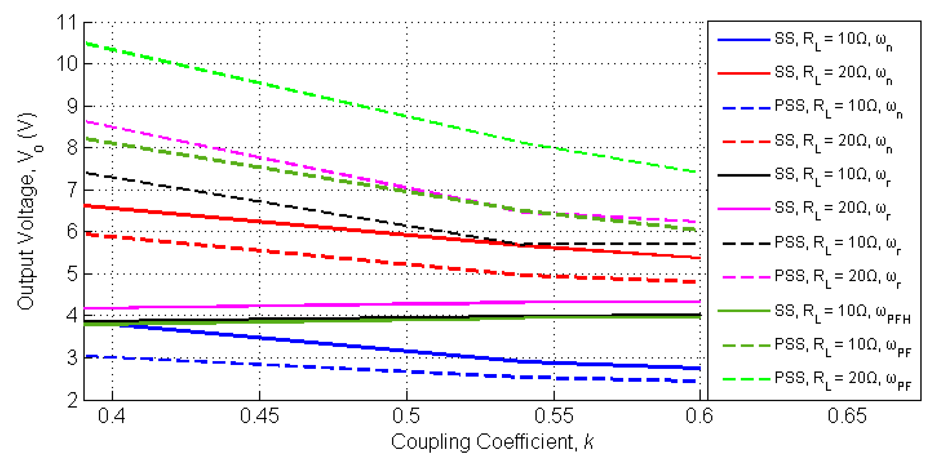
For clearer illustration and better comparison purposes, the experimental output voltage results of both topologies for each frequency of operation are depicted in Figure 12. As can be seen, the experimental results are in good agreement with the simulation results. The slight differences are attributed to the frequency differences mentioned previously, as well as the higher internal resistances of the experimental components.
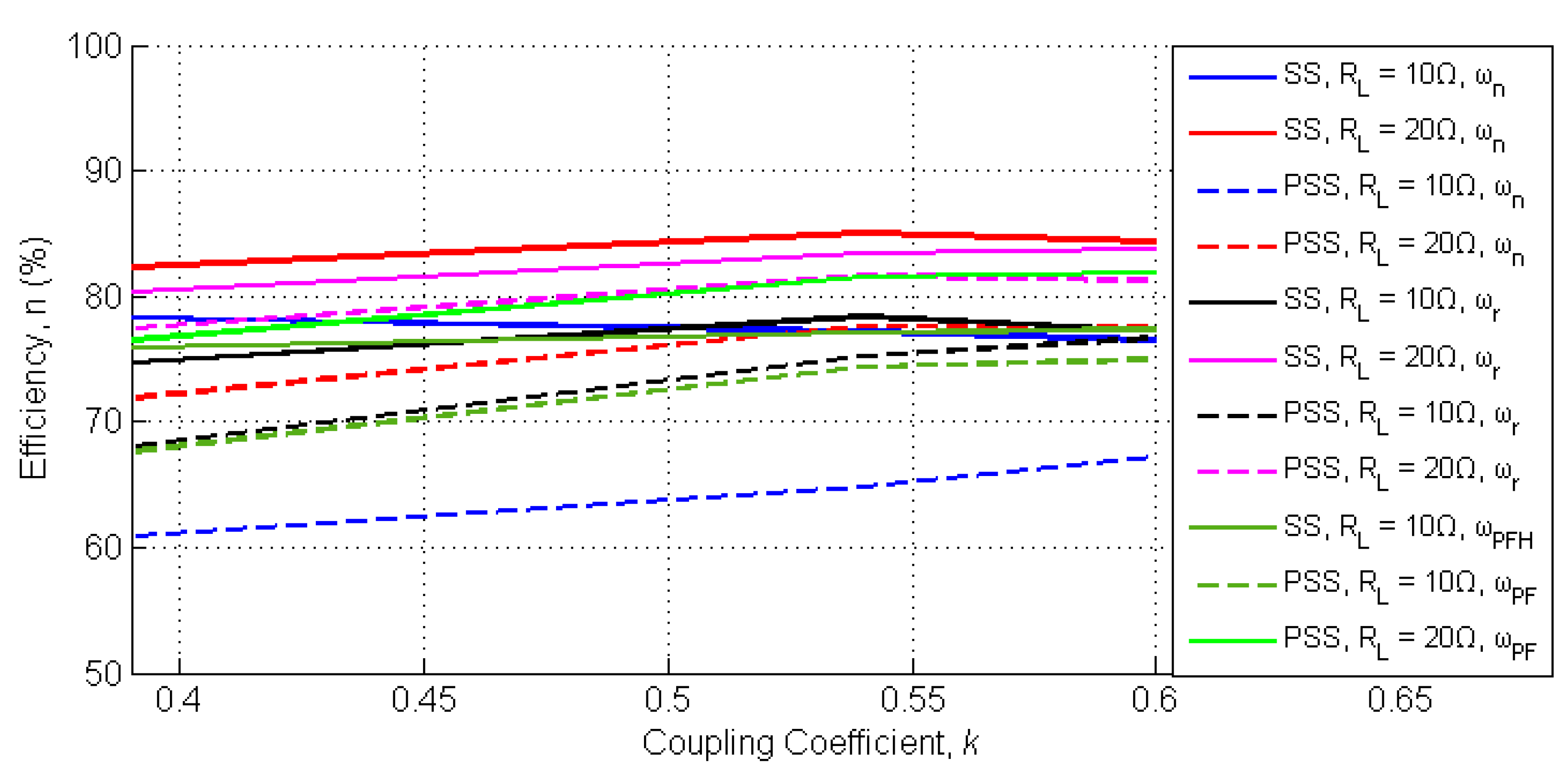
The DC/DC efficiency (measured at the points indicated in Figure 2) for both topologies, with respect to load and coupling coefficient values, is illustrated in Figure 13. As expected, the SS topology exhibits higher efficiency than the PSS, especially for the lower load value and for the lower coupling conditions. As the load value increases (which means that the battery is filling up) this difference in the efficiency is decreased. In these conditions, the minimal PSS topology presents satisfactory efficiency levels of around 80%, which can be further increased by constructing application-specific coils with reduced internal resistances. The achieved efficiency of the prototype is satisfactory as it reaches the highest recorded in literature for similar systems [31]. It is worth mentioning that, according to relevant studies, efficiency is expected to slightly improve in the case of actual implantation on the secondary side, since the human tissues are characterized by higher conductivity and permittivity values than free air [10,30].
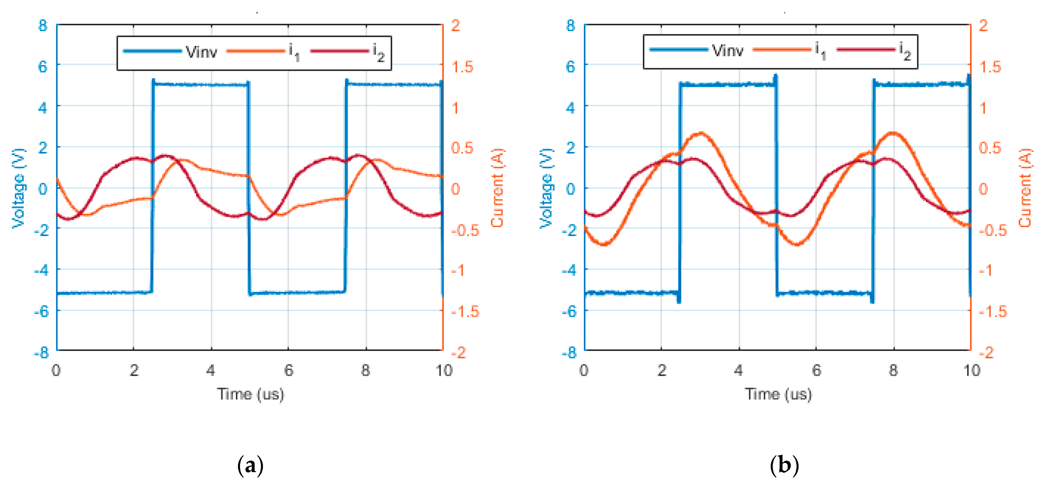
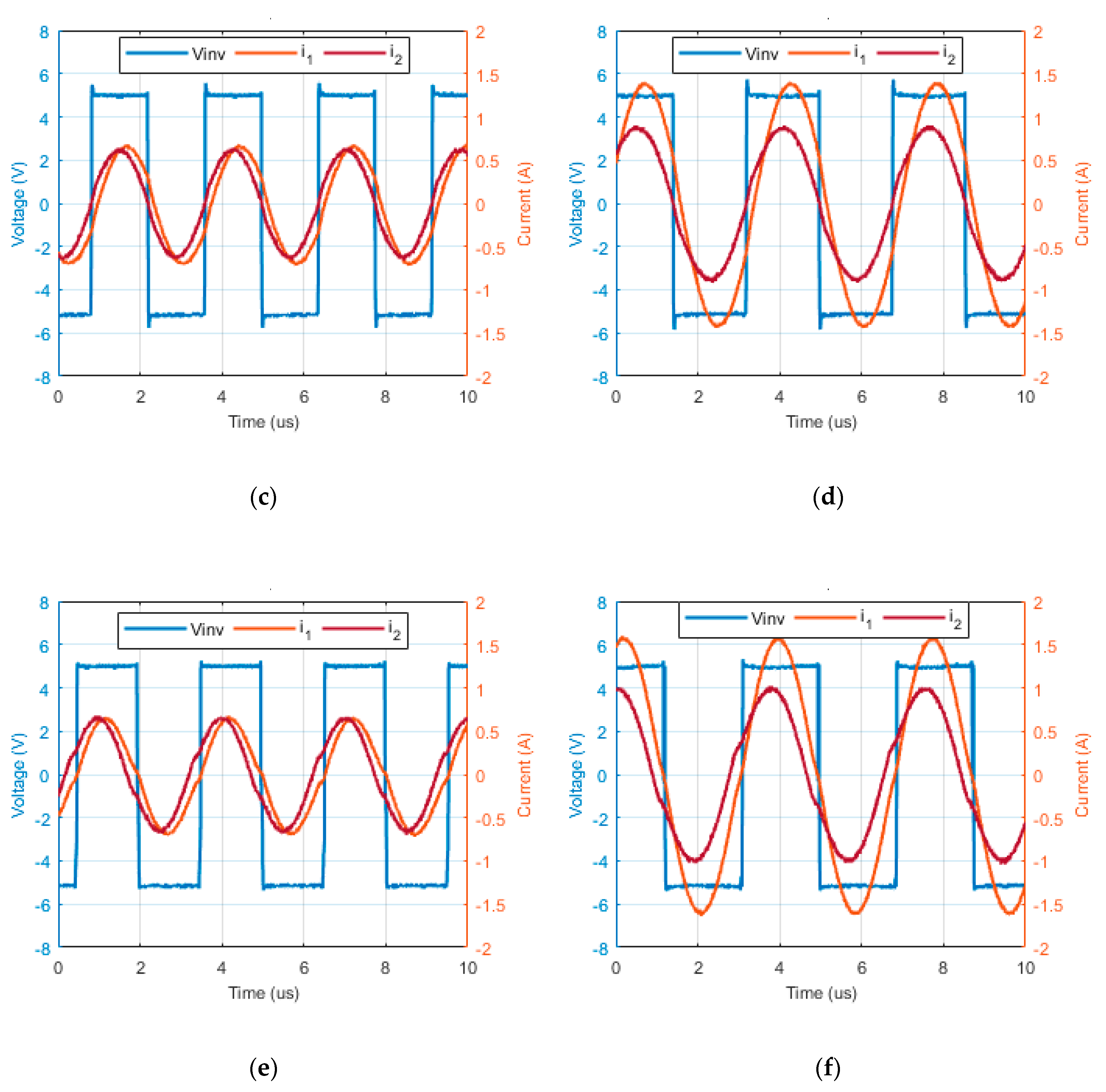
The experimentally obtained waveforms of the inverter output voltage, vinv, the primary side current, i1, and the secondary side current, i2, for the two topologies are recorded in Figure 14. These experiments were carried out for k = 0.6 and RL = 10 Ω for all the examined frequencies of operation.
In Figure 14a,b, the operation at ωn is recorded for the SS and PSS topology, respectively. In this frequency and for the specific load and coupling conditions, both currents are not sinusoidal. However, simulations and experiments show that the current waveforms get a more sinusoidal form as the load increases or as the coupling decreases.
Figure 14c,d illustrate operation at ωr, where the secondary-side current is in phase with the inverter output voltage. In this frequency of operation, the experimental results show almost equal efficiency for both topologies.
Finally, in Figure 14e,f, operation at ωPFH is recorded for the SS topology and at ωPF for the PSS topology. In these conditions, the primary-side current is in phase with the inverter output voltage. All zero-phase conditions lead to operation with sinusoidal currents.
Another important point for the application, that was confirmed through the simulations and experiments, is that the omission of the capacitor on the implanted side of the system is also beneficial for the patient since it removes one component on which a high differential voltage is developed due to the operation at resonance. What was also noticed is that the differential voltage developed on the implanted coil of the PSS system was in many cases, especially at lower couplings and higher loads, significantly lower (even up to three times) than the voltage across the coil when the secondary capacitor was present (SS topology). This factor is important for this specific application due to the extra sensitivity to the effects of the electric field on human tissue and the patient safety.
6. Conclusions
In this work, a minimal topology for inductive chargers used for implantable devices is investigated against the typical series-series compensation topology. The compensating capacitor is omitted from the secondary-side of the system of the former. With this arrangement, reduction of the component count is achieved in the implantable side and, as a result, the system reliability and lifetime is expected to increase.
Theoretical analysis and simulations showed that for operation at the natural frequency of the resonant circuit, in terms of output voltage, the primary-side series compensation topology yields almost the same results as the commonly used series-series compensation topology. Due to the fact that at ωn the output voltage depends on the coupling coefficient and the load value, adoption of an output power control technique may be necessary.
The same is valid for operation at all other examined frequencies, with the exception of ωr, and only for the SS topology, for which the output voltage can be maintained at a constant value, since it is equal to the input voltage and independent of the coupling and load conditions. However, this is achievable on condition that there is real-time communication with the implanted side of the system so as to constantly adjust the frequency of operation.
With regard to operation at the frequency for which the primary current is in phase with the inverter output voltage, it must be noted that the frequency control strategy employed will have to deal with the bifurcation phenomenon. Otherwise, there may be uncontrollable switching among the zero-phase frequencies, which will ultimately lead to abrupt variation of the output voltage of the charger. In this case the PSS topology presents a strong benefit, since it provides a single zero-phase angle between the primary current and the inverter output voltage.
However, the stable operation of the PSS topology comes at the cost of lower efficiency with respect to the SS one. Keeping in mind that chargers of implantable devices operate at low power levels (typically from below 1 W to a few W), the choice between higher reliability or higher efficiency lies with the designer and the specificities of each application. For instance, there are biomedical devices, like cochlear implants, for which the patient is constantly carrying both the primary system (attached but not implanted) and the secondary system (implanted), and the primary is wirelessly feeding the secondary system with the use of an external battery. In these types of biomedical applications, the system efficiency is of great importance, since the attached primary has to incorporate a very small sized battery and it is more convenient for the patient if the recharging of this battery is infrequent. Therefore, in such cases, the use of the SS compensation topology can be the best option, since achieving the highest possible efficiency is of the utmost importance. On the contrary, in applications for which reliability of the wireless power transfer is the most important aspect, like in LVADs, because the constant feeding of the implanted device is crucial for the patient’s life, carrying a slightly heavier external battery can be less important than ensuring higher reliability of the system. In the majority of biomedical applications, such as pacemakers, etc., efficiency is not a key factor, since the primary side of the charger is not attached to the patient and the system can be powered by a portable device with a large battery or straight from the grid. In these cases, the PSS topology can be a preferable option for inductive power transfer systems.
As an overall assessment, the present investigation can safely conclude that the PSS topology is a strong option for the replacement of the series-series compensation topology, as the benefits it has shown are highly important for biomedical applications, whereas its disadvantages do not play such a crucial role for these systems.
Author Contributions
Conceptualization and methodology, E.G. and S.K.; software, S.K.; validation and investigation, S.K., E.G., and N.P.; formal analysis, E.G. and N.P.; writing—original draft preparation, E.G.; writing—review and editing, S.K., N.P., and S.M.; supervision and project administration, S.M. All authors have read and agreed to the published version of the manuscript.
Funding
This research was carried out in the context of the project “Advanced wireless charging techniques for medical implant applications” (MIS 5004934) under the call for proposals “Supporting Researchers with an Emphasis on Young Researchers” (EDULLL 34). The project was co-financed by Greece and the European Union (European Social Fund- ESF) by the Operational Programme Human Resources Development, Education and Lifelong Learning 2014-2020.

Conflicts of Interest
The authors declare no conflicts of interest.
References
- Raatikainen, M.J.P.; Arnar, D.O.; Zeppenfeld, K.; Merino, J.L.; Levya, F.; Hindriks, G.; Kuck, K.-H. Statistics on the use of cardiac electronic devices and electrophysiological procedures in the European Society of Cardiology countries: 2014 report from the European Heart Rhythm Association. Europace 2015, 17, i1–i75. [Google Scholar] [CrossRef] [PubMed] [Green Version]
- Campi, T.; Cruciani, S.; Palandrani, F.; De Santis, V.; Hirata, A.; Feliziani, M. Wireless Power Transfer Charging System for AIMDs and Pacemakers. IEEE Trans. Microw. Theory Tech. 2016, 64, 633–642. [Google Scholar] [CrossRef]
- Knecht, O.; Bosshard, R.; Kolar, J.W. High-Efficiency Transcutaneous Energy Transfer for Implantable Mechanical Heart Support Systems. IEEE Trans. Power Electron. 2015, 30, 6221–6236. [Google Scholar] [CrossRef]
- Knecht, O.; Kolar, J.W. Performance Evaluation of Series-Compensated IPT Systems for Transcutaneous Energy Transfer. IEEE Trans. Power Electron. 2019, 34, 438–451. [Google Scholar] [CrossRef]
- Nair, V.; Choi, J. An Integrated Chip High-Voltage Power Receiver for Wireless Biomedical Implants. Energies 2015, 8, 5467–5487. [Google Scholar] [CrossRef] [Green Version]
- Agarwal, K.; Jegadeesan, R.; Guo, Y.-X.; Thakor, N.V. Wireless Power Transfer Strategies for Implantable Bioelectronics. IEEE Rev. Biomed. Eng. 2017, 10, 136–161. [Google Scholar] [CrossRef] [PubMed]
- Amar, A.; Kouki, A.; Cao, H. Power Approaches for Implantable Medical Devices. Sensors 2015, 15, 28889–28914. [Google Scholar] [CrossRef] [PubMed]
- Xu, G.; Yang, X.; Yang, Q.; Zhao, J.; Li, Y. Design on Magnetic Coupling Resonance Wireless Energy Transmission and Monitoring System for Implanted Devices. IEEE Trans. Appl. Supercond. 2016, 26, 1–4. [Google Scholar] [CrossRef]
- Ho, J.S.; Kim, S.; Poon, A.S.Y. Midfield Wireless Powering for Implantable Systems. Proc. IEEE 2013, 101, 1369–1378. [Google Scholar] [CrossRef]
- Chandima, D.P.; Dayarathna, K.D.U.; Jayasinghe, H.G.D.; Dharmasiri, W.K.K.; Weerasinghe, H. Inductive power transmission, charging and communication for implantable devices. In Proceedings of the 2017 IEEE International Conference on Industrial and Information Systems (ICIIS), Peradeniya, Sri Lanka, 15–16 December 2017; pp. 1–6. [Google Scholar]
- Knecht, O.; Kolar, J.W. Impact of Transcutaneous Energy Transfer on the electric field and specific absorption rate in the human tissue. In Proceedings of the IECON 2015—41st Annual Conference of the IEEE Industrial Electronics Society, Yokohama, Japan, 9–12 November 2015; pp. 004977–004983. [Google Scholar]
- Bakogianni, S.; Koulouridis, S. Sub-1 GHz far-field powering of implantable medical devices: Design and safety considerations. In Proceedings of the 2015 IEEE International Symposium on Antennas and Propagation & USNC/URSI National Radio Science Meeting, Vancouver, BC, Canada, 19–24 July 2015; Volume 2015-Octob, pp. 942–943. [Google Scholar]
- Lucke, L.; Bluvshtein, V. Safety considerations for wireless delivery of continuous power to implanted medical devices. In Proceedings of the 2014 36th Annual International Conference of the IEEE Engineering in Medicine and Biology Society, Chicago, IL, USA, 26–30 August 2014; Volume 2014, pp. 286–289. [Google Scholar]
- Koulouridis, S.; Bakogianni, S.; Diet, A.; Le Bihan, Y.; Pichon, L. Investigation of efficient wireless charging for deep implanted medical devices. In Proceedings of the 2016 IEEE International Symposium on Antennas and Propagation (APSURSI), Fajardo, Puerto Rico, 26 June–1 July 2016; pp. 1045–1046. [Google Scholar]
- Ho, J.S.; Yeh, A.J.; Neofytou, E.; Kim, S.; Tanabe, Y.; Patlolla, B.; Beygui, R.E.; Poon, A.S.Y. Wireless power transfer to deep-tissue microimplants. Proc. Natl. Acad. Sci. USA 2014, 111, 7974–7979. [Google Scholar] [CrossRef] [PubMed] [Green Version]
- Ahn, D.; Ghovanloo, M. Optimal Design of Wireless Power Transmission Links for Millimeter-Sized Biomedical Implants. IEEE Trans. Biomed. Circuits Syst. 2016, 10, 125–137. [Google Scholar] [CrossRef] [PubMed]
- RamRakhyani, A.K.; Mirabbasi, S.; Chiao, M. Design and Optimization of Resonance-Based Efficient Wireless Power Delivery Systems for Biomedical Implants. IEEE Trans. Biomed. Circuits Syst. 2011, 5, 48–63. [Google Scholar] [CrossRef] [PubMed]
- Liu, X.; Ng, W.M.; Lee, C.K.; Hui, S.Y. Optimal operation of contactless transformers with resonance in secondary circuits. In Proceedings of the 2008 Twenty-Third Annual IEEE Applied Power Electronics Conference and Exposition, Austin, TX, USA, 24–28 February 2008; Volume 2, pp. 645–650. [Google Scholar]
- Pedder, D.; Brown, A.; Skinner, J.A. A contactless electrical energy transmission system. IEEE Trans. Ind. Electron. 1999, 46, 23–30. [Google Scholar] [CrossRef]
- Gati, E.; Kampitsis, G.; Stavropoulos, I.; Papathanassiou, S.; Manias, S. Wireless Phase—Locked Loop control for inductive Power Transfer Systems. In Proceedings of the 2015 IEEE Applied Power Electronics Conference and Exposition (APEC), Charlotte, NC, USA, 15–19 March 2015; pp. 1601–1607. [Google Scholar]
- Zhang, W.; Mi, C.C. Compensation Topologies of High-Power Wireless Power Transfer Systems. IEEE Trans. Veh. Technol. 2016, 65, 4768–4778. [Google Scholar] [CrossRef]
- Gati, E.; Kampitsis, G.; Manias, S. Variable Frequency Controller for Inductive Power Transfer in Dynamic Conditions. IEEE Trans. Power Electron. 2017, 32, 1684–1696. [Google Scholar] [CrossRef]
- Song, K.; Li, Z.; Du, Z.; Wei, G.; Zhu, C. Design for constant output voltage and current controllability of primary side controlled wireless power transfer system. In Proceedings of the 2017 IEEE PELS Workshop on Emerging Technologies: Wireless Power Transfer (WoW), Chongqing, China, 20–22 May 2017; pp. 1–6. [Google Scholar]
- Chen, G.; Sun, Y.; Huang, J.; Zhou, B.; Meng, F.; Tang, C. Wireless Power and Data Transmission System of Submarine Cable-Inspecting Robot Fish and Its Time-Sharing Multiplexing Method. Electronics 2019, 8, 838. [Google Scholar] [CrossRef] [Green Version]
- Manias, S. Power Electronics and Motor Drive Systems; Academic Press, Elsevier Inc.: Cambridge, MA, USA, 2017; ISBN 978-0-12-811798-9. [Google Scholar]
- Wang, C.-S.; Covic, G.A.; Stielau, O.H. Power Transfer Capability and Bifurcation Phenomena of Loosely Coupled Inductive Power Transfer Systems. IEEE Trans. Ind. Electron. 2004, 51, 148–157. [Google Scholar] [CrossRef]
- Boys, J.T.; Covic, G.A.; Green, A.W. Stability and control of inductively coupled power transfer systems. IEE Proc. Electr. Power Appl. 2000, 147, 37. [Google Scholar] [CrossRef]
- Gore, V.B.; Gawali, D.H. Wireless power transfer technology for medical applications. In Proceedings of the 2016 Conference on Advances in Signal Processing (CASP), Pune, India, 9–11 June 2016; pp. 455–460. [Google Scholar]
- Amasha, H.M.; Ghazzawi, Z.K.; Al-Nabulsi, J.I. A wireless multi bundle concentric coil for charging the battery of a total artificial heart or a pacemaker. Comput. Cardiol. 2007, 34, 201–204. [Google Scholar]
- Xiao, C.; Wei, K.; Cheng, D.; Liu, Y. Wireless Charging System Considering Eddy Current in Cardiac Pacemaker Shell: Theoretical Modeling, Experiments, and Safety Simulations. IEEE Trans. Ind. Electron. 2017, 64, 3978–3988. [Google Scholar] [CrossRef]
- Lu, Y.; Jiang, H.; Mai, S.; Wang, Z. A wireless charging circuit with high power efficiency and security for implantable devices. In Proceedings of the 2016 IEEE Biomedical Circuits and Systems Conference (BioCAS), Shanghai, China, 17–19 October 2016; pp. 328–331. [Google Scholar]
Figure 1.
Equivalent circuits of inductive power transfer systems with (a) series-series, (b) parallel-series (c) series-parallel, and (d) parallel-parallel compensation.
Figure 1.
Equivalent circuits of inductive power transfer systems with (a) series-series, (b) parallel-series (c) series-parallel, and (d) parallel-parallel compensation.

Figure 2.
Block diagram of inductive power transfer systems (IPTSs) with (a) series-series compensation and (b) primary-side series compensation.
Figure 2.
Block diagram of inductive power transfer systems (IPTSs) with (a) series-series compensation and (b) primary-side series compensation.

Figure 3.
First harmonic equivalent circuit of (a) series-series compensated IPTS and (b) primary-side series compensated IPTS.
Figure 3.
First harmonic equivalent circuit of (a) series-series compensated IPTS and (b) primary-side series compensated IPTS.

Figure 4.
(a) Three-dimensional (3D) design of primary and secondary side coils and (b) experimental setup coils.
Figure 4.
(a) Three-dimensional (3D) design of primary and secondary side coils and (b) experimental setup coils.

Figure 5.
Leakage equivalent circuit of inductively coupled coils.

Figure 6.
Coupling coefficient, k, for various positions.

Figure 7.
(a) Output power of the series-series (SS) and primary-side series (PSS) topology for R = 10 Ω and k = 0.6 m, (b) phase difference between the inverter output voltage and the primary-side current and, (c) phase difference between the inverter output voltage and the secondary-side current.
Figure 7.
(a) Output power of the series-series (SS) and primary-side series (PSS) topology for R = 10 Ω and k = 0.6 m, (b) phase difference between the inverter output voltage and the primary-side current and, (c) phase difference between the inverter output voltage and the secondary-side current.

Figure 8.
Comparison of output voltage with respect to coupling coefficient for various load resistances for operation at ωn (f = 200 kHz).
Figure 8.
Comparison of output voltage with respect to coupling coefficient for various load resistances for operation at ωn (f = 200 kHz).

Figure 9.
Comparison of output voltage with respect to coupling coefficient for various load resistances for operation at ωr.
Figure 9.
Comparison of output voltage with respect to coupling coefficient for various load resistances for operation at ωr.

Figure 10.
Comparison of output voltage with respect to coupling coefficient for various load resistances for operation at ωPF.
Figure 10.
Comparison of output voltage with respect to coupling coefficient for various load resistances for operation at ωPF.

Figure 11.
Experimental setup.

Figure 12.
Experimentally measured output voltage for various coupling coefficients and load values for the SS and PSS topologies.
Figure 12.
Experimentally measured output voltage for various coupling coefficients and load values for the SS and PSS topologies.

Figure 13.
Experimentally measured DC/DC efficiency for various coupling coefficients and load values for the SS and PSS topologies.
Figure 13.
Experimentally measured DC/DC efficiency for various coupling coefficients and load values for the SS and PSS topologies.

Figure 14.
Experimental results for RL = 10 Ω, k = 0.6, and operation at (a) ωn for the SS topology, (b) ωn for the PSS topology, (c) ωr for the SS topology, (d) ωr for the PSS topology, (e) ωPFH for the SS topology, and (f) ωPF for the PSS topology.
Figure 14.
Experimental results for RL = 10 Ω, k = 0.6, and operation at (a) ωn for the SS topology, (b) ωn for the PSS topology, (c) ωr for the SS topology, (d) ωr for the PSS topology, (e) ωPFH for the SS topology, and (f) ωPF for the PSS topology.


Table 1.
Component values for simulations.
| Parameter | Value | Parameter | Value |
|---|---|---|---|
| L1, L2 | 20 μH | C1, C2 | 31.7 nF |
| k | 0.63–0.09 | RL | 10 Ω–50 Ω |
| VDC | 5 V | fn | 200 kHz |
| R1, R2 | 0.5 Ω | Po,nom | 2 W |
Table 2.
Evaluated frequencies for operation at ωr.
| SS | PSS | ||||||
|---|---|---|---|---|---|---|---|
| k | f (kHz) | k | f (kHz) | k | f (kHz) | k | f (kHz) |
| 0.63 | 328.6 | 0.35 | 247.9 | 0.63 | 257.4 | 0.35 | 213.4 |
| 0.60 | 316.0 | 0.30 | 238.9 | 0.60 | 249.9 | 0.30 | 209.5 |
| 0.55 | 298.0 | 0.25 | 230.8 | 0.55 | 239.3 | 0.25 | 206.4 |
| 0.50 | 282.7 | 0.20 | 223.5 | 0.50 | 230.8 | 0.20 | 204.0 |
| 0.45 | 269.5 | 0.15 | 216.8 | 0.45 | 223.8 | 0.15 | 202.2 |
| 0.40 | 258.1 | 0.09 | 209.5 | 0.40 | 218.1 | 0.09 | 200.7 |
Table 3.
Evaluated frequencies (kHz) for operation of the SS topology at ωPFH.
| k | 0.63 | 0.6 | 0.55 | 0.5 | 0.45 | 0.4 | 0.35 | 0.3 | 0.25 | 0.2 | 0.15 | 0.09 | |
|---|---|---|---|---|---|---|---|---|---|---|---|---|---|
| RL (Ω) | |||||||||||||
| 10 | 320.5 | 308.1 | 290.3 | 275.1 | 262.1 | 250.6 | 240.5 | 231.5 | 223.4 | 216.0 | 209.2 | 201.8 | |
| 15 | 310.1 | 297.9 | 280.3 | 265.3 | 252.4 | 241.1 | 231.0 | 221.9 | 213.7 | 206.2 | 199.3 | 191.6 | |
| 20 | 294.9 | 283.0 | 265.8 | 251.0 | 238.2 | 227.0 | 216.9 | 207.7 | 199.4 | 191.7 | 184.5 | 176.5 | |
| 30 | 246.4 | 235.3 | 218.9 | 204.7 | 192.1 | 180.7 | 170.3 | 160.5 | 151.2 | 142.3 | 133.6 | 123.2 | |
| 40 | 154.9 | 144.0 | 127.1 | 111.2 | 95.5 | 79.2 | 61.1 | 37.5 | n/a | n/a | n/a | n/a | |
| 50 | n/a | n/a | n/a | n/a | n/a | n/a | n/a | n/a | n/a | n/a | n/a | n/a | |
Table 4.
Evaluated frequencies (kHz) for operation of the SS topology at ωPFL.
| k | 0.63 | 0.6 | 0.55 | 0.5 | 0.45 | 0.4 | 0.35 | 0.3 | 0.25 | 0.2 | 0.15 | 0.09 | |
|---|---|---|---|---|---|---|---|---|---|---|---|---|---|
| RL (Ω) | |||||||||||||
| 10 | 138.8 | 141.5 | 145.7 | 149.7 | 153.6 | 157.4 | 161.2 | 165.1 | 169.1 | 173.2 | 177.5 | 182.9 | |
| 15 | 112.7 | 117.6 | 124.7 | 130.9 | 136.5 | 141.6 | 146.5 | 151.3 | 156.1 | 160.9 | 165.7 | 171.7 | |
| 20 | 59.3 | 72.0 | 87.3 | 98.7 | 108.0 | 116.0 | 123.1 | 129.7 | 135.8 | 141.8 | 147.6 | 154.5 | |
| 30 | n/a | n/a | n/a | n/a | n/a | n/a | n/a | n/a | 39.6 | 60.1 | 74.8 | 89.0 | |
| 40 | n/a | n/a | n/a | n/a | n/a | n/a | n/a | n/a | n/a | n/a | n/a | n/a | |
| 50 | n/a | n/a | n/a | n/a | n/a | n/a | n/a | n/a | n/a | n/a | n/a | n/a | |
Table 5.
Evaluated frequencies (kHz) for operation of the PSS topology at ωPF.
| k | 0.63 | 0.6 | 0.55 | 0.5 | 0.45 | 0.4 | 0.35 | 0.3 | 0.25 | 0.2 | 0.15 | 0.09 | |
|---|---|---|---|---|---|---|---|---|---|---|---|---|---|
| RL (Ω) | |||||||||||||
| 10 | 249.9 | 243.3 | 234.1 | 226.7 | 220.6 | 215.6 | 211.6 | 208.2 | 205.5 | 203.4 | 201.9 | 200.6 | |
| 15 | 242.3 | 236.7 | 229.0 | 222.7 | 217.5 | 213.3 | 209.8 | 207.0 | 204.7 | 202.9 | 201.6 | 200.5 | |
| 20 | 234.2 | 229.8 | 223.6 | 218.5 | 214.4 | 210.9 | 208.1 | 205.8 | 203.9 | 202.4 | 201.3 | 200.4 | |
| 30 | 221.2 | 218.6 | 215.0 | 211.9 | 209.3 | 207.1 | 205.3 | 203.8 | 202.5 | 201.6 | 200.8 | 200.2 | |
| 40 | 213.5 | 211.9 | 209.7 | 207.8 | 206.1 | 204.7 | 203.5 | 202.5 | 201.7 | 201.0 | 200.5 | 200.1 | |
| 50 | 209.1 | 208.1 | 206.6 | 205.4 | 204.2 | 203.3 | 202.4 | 201.7 | 201.2 | 200.7 | 200.3 | 200.0 | |
Table 6.
Experimental measurements of the series-series compensated topology.
| k | ω | f (kHz) | RL | VDC,in | IDC,in | Pin | Vo | Po | n |
|---|---|---|---|---|---|---|---|---|---|
| 0.60 | ωn | 200 | 10 | 5.01 | 0.19 | 0.95 | 2.76 | 0.73 | 76.58% |
| ωr | 360 | 5.06 | 0.40 | 2.02 | 4.03 | 1.56 | 77.32% | ||
| ωPFH | 330 | 5.06 | 0.39 | 1.97 | 3.94 | 1.53 | 77.42% | ||
| ωn | 200 | 20 | 5.02 | 0.33 | 1.66 | 5.38 | 1.40 | 84.40% | |
| ωr | 360 | 5.01 | 0.21 | 1.05 | 4.32 | 0.88 | 83.85% | ||
| ωPFH | - | - | - | - | - | - | - | ||
| 0.54 | ωn | 200 | 10 | 5.02 | 0.21 | 1.06 | 2.91 | 0.81 | 77.23% |
| ωr | 340 | 5.01 | 0.39 | 1.95 | 3.99 | 1.53 | 78.45% | ||
| ωPFH | 300 | 5.08 | 0.39 | 1.98 | 3.94 | 1.53 | 77.16% | ||
| ωn | 200 | 20 | 5.04 | 0.36 | 1.82 | 5.68 | 1.54 | 85.08% | |
| ωr | 340 | 5.02 | 0.21 | 1.06 | 4.32 | 0.88 | 83.53% | ||
| ωPFH | - | - | - | - | - | - | - | ||
| 0.39 | ωn | 200 | 10 | 5.06 | 0.37 | 1.87 | 3.86 | 1.47 | 78.38% |
| ωr | 280 | 5.04 | 0.39 | 1.97 | 3.87 | 1.47 | 74.82% | ||
| ωPFH | 230 | 5.03 | 0.37 | 1.86 | 3.80 | 1.41 | 75.97% | ||
| ωn | 200 | 20 | 5.01 | 0.52 | 2.61 | 6.63 | 2.15 | 82.41% | |
| ωr | 280 | 5.06 | 0.21 | 1.06 | 4.19 | 0.85 | 80.41% | ||
| ωPFH | 205 | 5.02 | 0.62 | 3.11 | 7.26 | 2.58 | 83.11% |
Table 7.
Experimental measurements of the primary-side series compensated topology.
| k | ω | f (kHz) | RL | VDCin | IDCin | Pin | Vo | Po | n |
|---|---|---|---|---|---|---|---|---|---|
| 0.60 | ωn | 200 | 10 | 5.08 | 0.17 | 0.86 | 2.46 | 0.58 | 67.24% |
| ωr | 280 | 5.04 | 0.82 | 4.13 | 5.70 | 3.17 | 76.76% | ||
| ωPF | 265 | 5.06 | 0.95 | 4.80 | 6.05 | 3.61 | 75.07% | ||
| ωn | 200 | 20 | 5.06 | 0.28 | 1.42 | 4.82 | 1.10 | 77.57% | |
| ωr | 280 | 5.01 | 0.46 | 2.31 | 6.25 | 1.88 | 81.33% | ||
| ωPF | 245 | 5.01 | 0.65 | 3.26 | 7.42 | 2.67 | 81.99% | ||
| 0.54 | ωn | 200 | 10 | 5.05 | 0.19 | 0.96 | 2.55 | 0.62 | 64.88% |
| ωr | 270 | 5.01 | 0.84 | 4.21 | 5.70 | 3.17 | 75.31% | ||
| ωPF | 252 | 5.03 | 1.12 | 5.63 | 6.51 | 4.19 | 74.42% | ||
| ωn | 200 | 20 | 5.03 | 0.30 | 1.51 | 4.97 | 1.17 | 77.73% | |
| ωr | 270 | 5.05 | 0.49 | 2.47 | 6.48 | 2.02 | 81.70% | ||
| ωPF | 240 | 5.05 | 0.78 | 3.94 | 8.12 | 3.22 | 81.63% | ||
| 0.39 | ωn | 200 | 10 | 5.04 | 0.29 | 1.46 | 3.05 | 0.89 | 60.99% |
| ωr | 233 | 5.07 | 1.53 | 7.76 | 7.42 | 5.28 | 68.11% | ||
| ωPF | 227 | 5.09 | 1.93 | 9.82 | 8.23 | 6.65 | 67.69% | ||
| ωn | 200 | 20 | 5.08 | 0.47 | 2.39 | 5.96 | 1.72 | 71.95% | |
| ωr | 233 | 5.05 | 0.91 | 4.60 | 8.65 | 3.56 | 77.55% | ||
| ωPF | 220 | 5.05 | 1.39 | 7.02 | 10.50 | 5.38 | 76.59% |
© 2019 by the authors. Licensee MDPI, Basel, Switzerland. This article is an open access article distributed under the terms and conditions of the Creative Commons Attribution (CC BY) license (http://creativecommons.org/licenses/by/4.0/).
Share and Cite
MDPI and ACS Style
Gati, E.; Kokosis, S.; Patsourakis, N.; Manias, S. Comparison of Series Compensation Topologies for Inductive Chargers of Biomedical Implantable Devices. Electronics 2020, 9, 8. https://0-doi-org.brum.beds.ac.uk/10.3390/electronics9010008
AMA Style
Gati E, Kokosis S, Patsourakis N, Manias S. Comparison of Series Compensation Topologies for Inductive Chargers of Biomedical Implantable Devices. Electronics. 2020; 9(1):8. https://0-doi-org.brum.beds.ac.uk/10.3390/electronics9010008
Chicago/Turabian StyleGati, Eleni, Sotirios Kokosis, Nikolaos Patsourakis, and Stefanos Manias. 2020. "Comparison of Series Compensation Topologies for Inductive Chargers of Biomedical Implantable Devices" Electronics 9, no. 1: 8. https://0-doi-org.brum.beds.ac.uk/10.3390/electronics9010008
Note that from the first issue of 2016, this journal uses article numbers instead of page numbers. See further details here.