Neuromorphic Computing Using Emerging Synaptic Devices: A Retrospective Summary and an Outlook


1
School of Computer Science and Electronic Engineering, Handong Global University, Pohang 37554, Korea
2
School of Electronic Engineering, Soongsil University, Seoul 06978, Korea
Electronics 2020, 9(9), 1414; https://0-doi-org.brum.beds.ac.uk/10.3390/electronics9091414
Submission received: 29 June 2020
/
Revised: 27 July 2020
/
Accepted: 5 August 2020
/
Published: 1 September 2020
(This article belongs to the Special Issue New CMOS Devices and Their Applications)
Abstract
:In this paper, emerging memory devices are investigated for a promising synaptic device of neuromorphic computing. Because the neuromorphic computing hardware requires high memory density, fast speed, and low power as well as a unique characteristic that simulates the function of learning by imitating the process of the human brain, memristor devices are considered as a promising candidate because of their desirable characteristic. Among them, Phase-change RAM (PRAM) Resistive RAM (ReRAM), Magnetic RAM (MRAM), and Atomic Switch Network (ASN) are selected to review. Even if the memristor devices show such characteristics, the inherent error by their physical properties needs to be resolved. This paper suggests adopting an approximate computing approach to deal with the error without degrading the advantages of emerging memory devices.
1. Introduction
Artificial Intelligence (AI), called machine intelligence, has been researched over the decades, and the AI now becomes an essential part of the industry [1,2,3]. Artificial intelligence means machines that imitate the cognitive functions of humans such as learning and problem solving [1,3]. Similarly, neuromorphic computing has been researched that imitates the process of the human brain compute and store [4,5,6]. Researches have been conducted to simulate human learning skills by mimicking the process the human brain learns using the computational structure of a computer in the form of an artificial neural network. Neuromorphic computing now has great attention from the industry because the neuromorphic computing efficiently executes artificial intelligence algorithms by imitating the brain nerve structure of humans.
The conventional von Neumann computing using individual processors and memory systems is not efficient for machine learning due to processor-memory bottlenecks [7,8,9,10]. Because the machine learning has a unique workload that iterates simple computation with large amounts of data, there should be huge data traffic between processors and memory subsystems. In contrast, the neuromorphic computing system consists of multiple neurons and synapses to compute and store data, and a neural network to communicate them. Therefore, this computing system can compute simple iterations efficiently for the training of machine learning [7,8]. For such a computing system, a new type of hardware is being researched and developed using next-generation emerging memory devices which also imitate neurons and synapses. In this paper, the neuromorphic computing system and promising emerging memory devices are reviewed, and the current issues and an outlook are discussed.
2. Neuromorphic Computing
2.1. History of Neuromorphic Computing
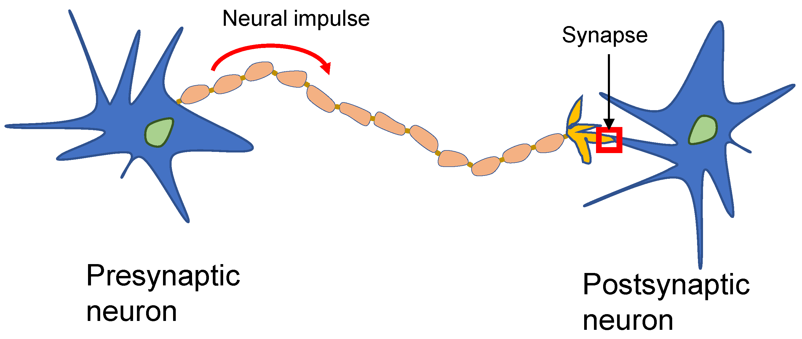
In the late 1980s, Professor Carver Mead proposed the concept of neuromorphic computing [11,12]. The computation process of computer hardware using transistors mimics the brain’s computation process on the neuromorphic computing. Over the decades, the concept has been studied by researchers to make machines that think and learn like humans in various forms. Studies have been conducted to simulate human learning skills using computer hardware in the form of an artificial neural network by mimicking the method the human brain learns and computes. The human brain has a very complex structure in which there are over a billion of neurons and trillions of synapses. Neurons consist of a cell body, an axon that produces neural signal impulse, and a dendrite that receives signals from other neurons as illustrated in Figure 1. A synapse is a structure that permits a neuron to deliver an electrical signal to another neuron.
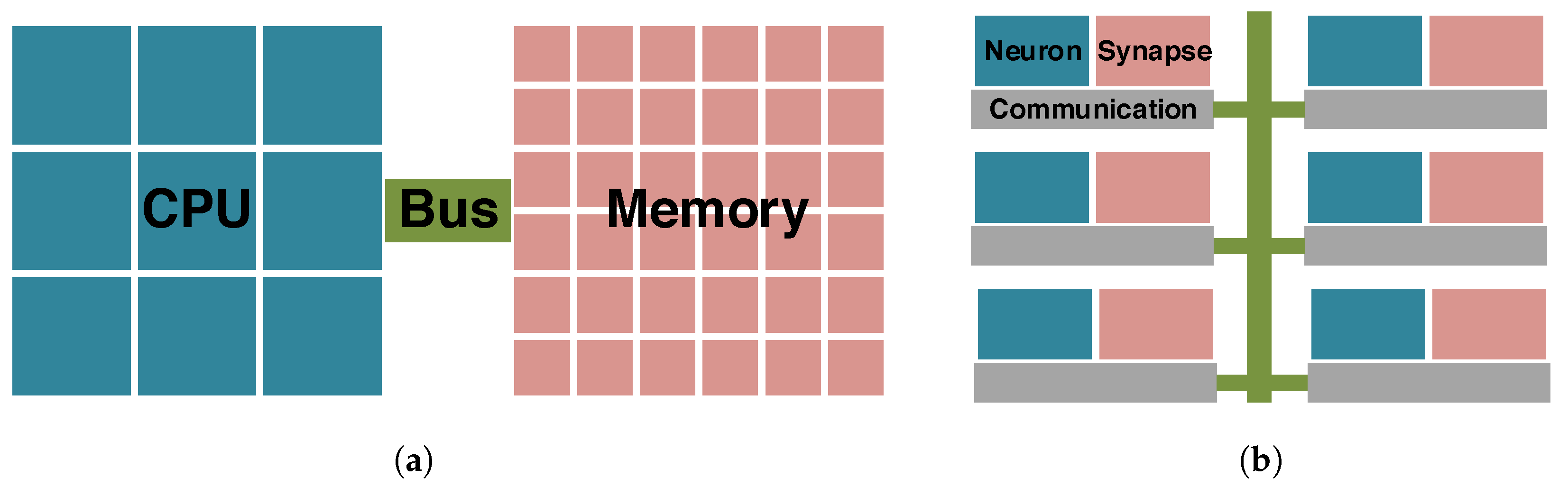
The neuromorphic hardware typically consists of neurons and synapses to imitate the nerve system of the human brain as shown in Figure 2b. In the neuromorphic hardware, each neuron is a core that processes data and, neurons are connected in parallel through synapses to transmit information [13,14,15]. There is no von Neumann bottleneck caused by having one signal bus in the neuromorphic hardware. To implement this in practical design, the development of artificial synaptic devices is necessary that reflect the characteristics of bio-synapses rather than conventional CMOS devices. Figure 2 shows the block diagram of the conventional von Neumann architecture and the emerging neuromorphic architecture.
2.2. An Outlook of Neuromorphic Computing
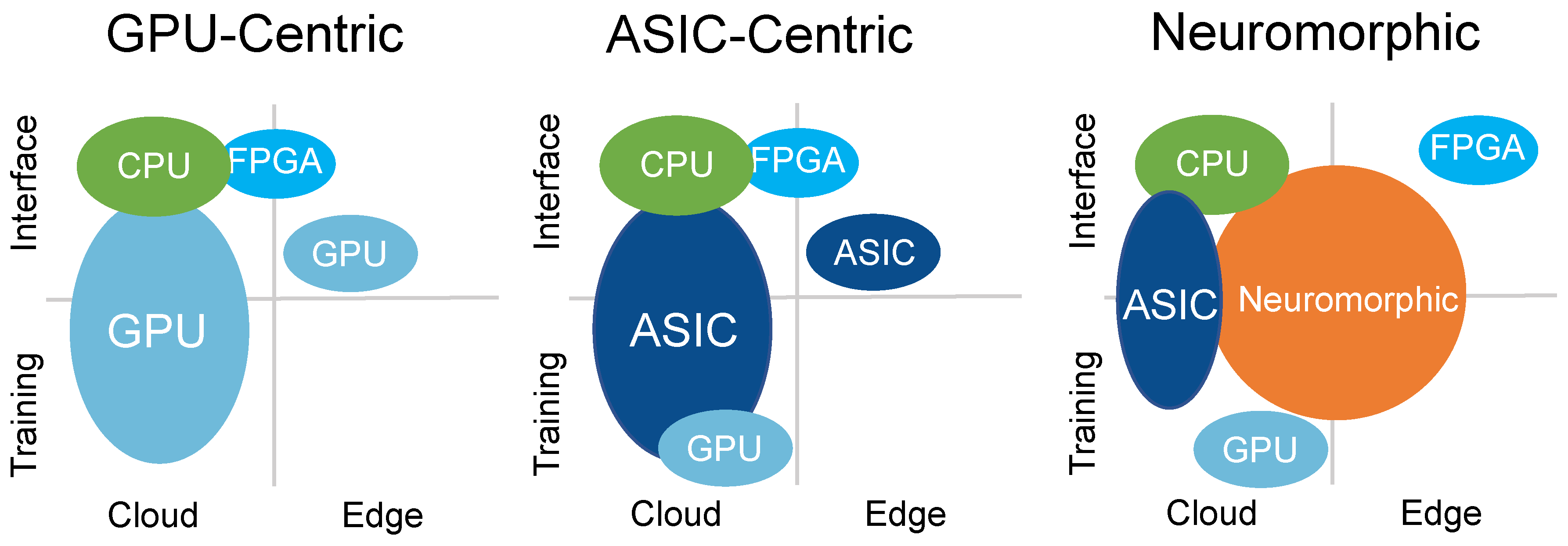
Neuromorphic computing has been researched over the decades, and recently, there would be significant advancements. The recent enhancement can be categorized with three major steps as shown in Figure 3 [16,17,18]. The first step is a GPU-Centric system that uses a graphics processing unit (GPU) to support artificial intelligence, optimized for parallel operation, and is mainly utilized in learning. The next step is an ASIC-Centric system which is now widely researched. This trend is expected to develop an efficient and low-power application-specific integrated circuit (ASIC) for machine learning. Therefore, many semiconductor companies are developing ASIC chips [19,20,21,22]. However, it is predicted that the neuromorphic computing will eventually evolve into neuromorphic hardware that enables ultra-low power and ultra-high performance computing to support for general-purpose artificial intelligence.
The neuromorphic-centric hardware needs to achieve simultaneous parallel processing of large volumes of data with ultra-low power. Furthermore, the neuromorphic semiconductor chip requires faster computation speed than the existing hardware that uses conventional CMOS devices. This implies developing an emerging synaptic device is key for the successful development of the neuromorphic-centric hardware. This paper describes promising emerging memory devices for the neuromorphic-centric hardware which also imitates the neurons and synapses that can simultaneously process storage and computation in the following sections.
3. Synaptic Emerging Memory Devices
Novel memory device technologies hold significant promise in providing new capabilities and opportunities for synaptic devices of the neuromorphic hardware. The synaptic memory devices are required to have high integration density, fast read speed, and low power. More importantly, the device imitating the characteristics of synapses needs to be a non-volatile storage, capable of expressing multiple levels of synapse strength, and easy to implement synaptic learning.
Memristor devices have been widely researched because the devices have such desirable characteristics [16,23,24,25]. This paper investigates the memristor devices as a promising synaptic device. The term, the memristor is a device that combines memory and a resistor. The device’s resistance is changed by voltage pulse applied to both ends and serves as a memory to store it for a certain period. In 1971 Professor Leon Chua predicted a fourth element other than a resistor, inductor, and capacitor whose relationship with charge and magnetic flux showed a nonlinear relationship [26]. Over the decades, various materials demonstrate the properties of the memristor such as Phase-change RAM (PRAM) ReRAM (Resistive RAM), and Magnetic RAM (MRAM) [27,28,29]. They implement the learning of synapses using characteristics that vary the resistance according to voltage pulses. PRAM is a non-volatile memory device that utilizes changes in resistance characteristics according to changes in the crystallinity of the material. ReRAM refers to a memory that utilizes analog resistance change, and MRAM exploits the resistance change from its spin direction. The memory devices have been touted as a promising candidate for a universal memory technology that may be able to provide integration density close to DRAM, the non-volatility of Flash memory, fast read speed close to SRAM, and practically zero standby power.
Moreover, the memory devices have a great potential to be a promising synaptic device that can process vast amounts of data efficiently with an ultra-low power, which is essential for the development of artificial intelligence technologies. The following sub-sections describe the detailed analysis of these memory devices including the current issues and the outlook.
3.1. PRAM: Phase-Change Synaptic Devices
Phase-change memory (PRAM), also called PCM, is a type of non-volatile random-access memory. In 1969, Charles Sie published a thesis that represents the feasibility of a phase-change-memory device by chalcogenide film with a diode [30]. The following study in 1970 established that the phase-change-memory mechanism in chalcogenide glass involves electric-field-induced crystalline filament growth [31,32].
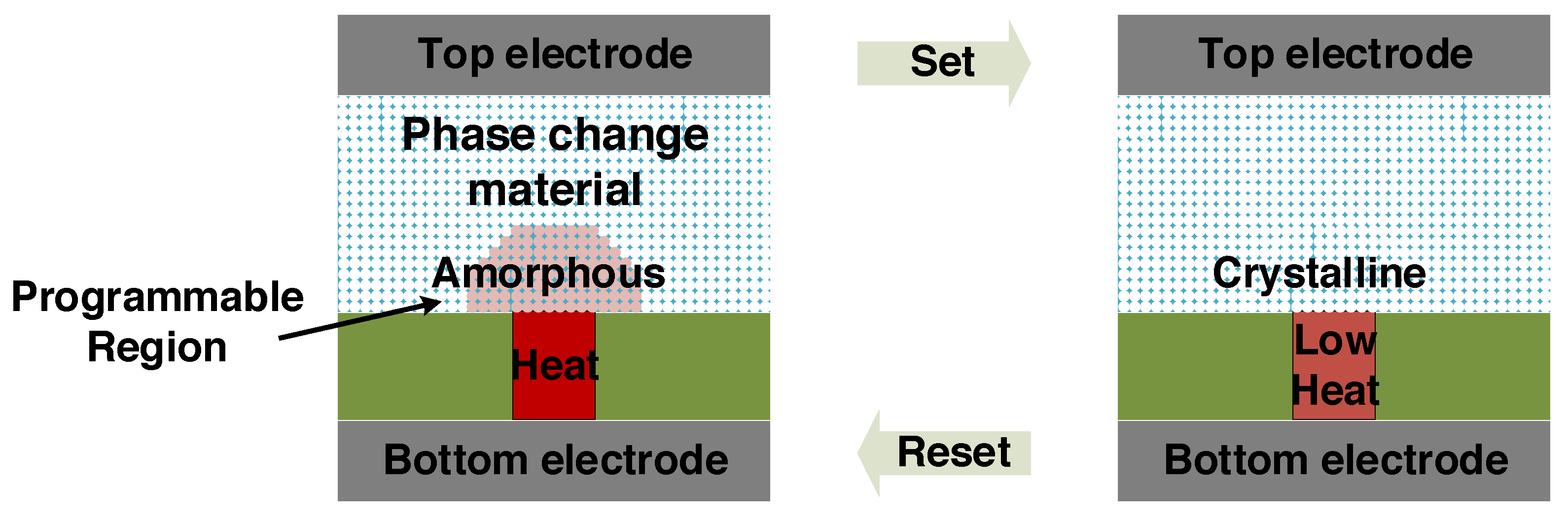
PRAM utilizes the difference of resistivity between the amorphous phase (high resistivity) and the crystalline phase (low resistivity) in phase change materials. PRAM is typically structured with a phase change material called T-cell between two electrodes as shown in Figure 4 [33,34,35]. Once a high voltage/current is applied to the electrodes, the phase of the material is changed. To Set into the crystalline phase, a current pulse is applied to anneal and quench the phase-change material to crystallize. The Set operation of PRAM devices may be created progressive by applying multiple Set pulses that incrementally crystallizes the high resistance amorphous part. To Reset into the amorphous phase, the programming region is first melted and then quenched rapidly by applying a large current pulse for a relatively short time.
Because of desirable characteristics such as high speed, multi-level capability, and low energy consumption, the device has been researched as a good candidate for artificial synapse in implementing the machine learning algorithm [36,37,38]. However, material quality and power consumption problems prevented the wide adoption of PRAM technology. Specifically, resistance drift is a significant challenge, meaning that the resistance is changed over time [39,40,41]. The resistance drift exists commonly in phase-change materials, and it destroys the stability and greatly limits the development of PRAM. The drift phenomenon in amorphous chalcogenide materials has been explained in terms of a structural relaxation which is a thermally-activated local rearrangement at intervals the amorphous section occurring shortly [40,42,43,44]. This means that the resistance can be modified over time, which implies a lost-memory appears to be almost like human memory. Apart from the major reliability issue in amorphous chalcogenide materials, the high power consumption for melting the phase-change material is also critical for a low power neuromorphic device. To be a good synapse device, PRAM technology needs to resolve these reliability and power issues.
3.2. Reram: Filament Type Synaptic Devices
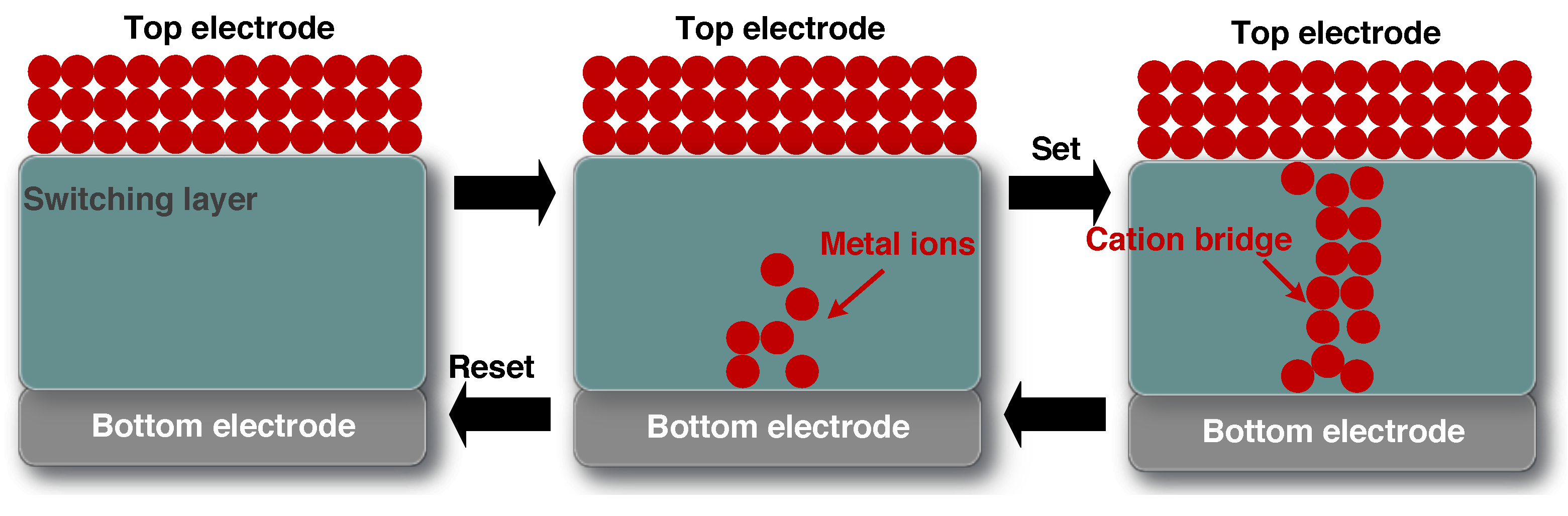
ReRAM (Resistive random-access memory) is one of the most representative next-generation non-volatile memory in which the resistance changes according to the applied voltage. ReRAM uses an insulator that can create a filament or conductivity path by voltage (Set operation) as shown in Figure 5 [45,46,47]. The conductivity path is formed (Set operation) by two mechanisms including vacancy or metal defect migration. The filament can be removed by another voltage (Reset operation). Each of these two states exhibits a distinct resistance corresponding to storing a binary ‘0’ or ‘1’.
ReRAM has many advantages such as good compatibility with the conventional CMOS processes, which reduces the development cost [46]. However, there are critical issues that need to be resolved for a memristor element. The filament formation of the ReRAM write process itself introduces variation and reliability problems. Specifically, the position or length in which the filament is formed is not controllable, making it difficult to adjust the resistance [47,48,49]. Therefore, the resistance’s variation over cells is huge, resulting in poor control of resistance. Furthermore, the resistance value changes over time. That means that it cannot maintain resistance values for a long time. While this issue may be possible to implement the short-term memory effects of synapses, it is difficult to implement long-term memory. However, this technical barrier may be a universal issue in synaptic devices as observed in PRAM, and the problem needs to be solved in circuit- and/or microarchitecture-level.
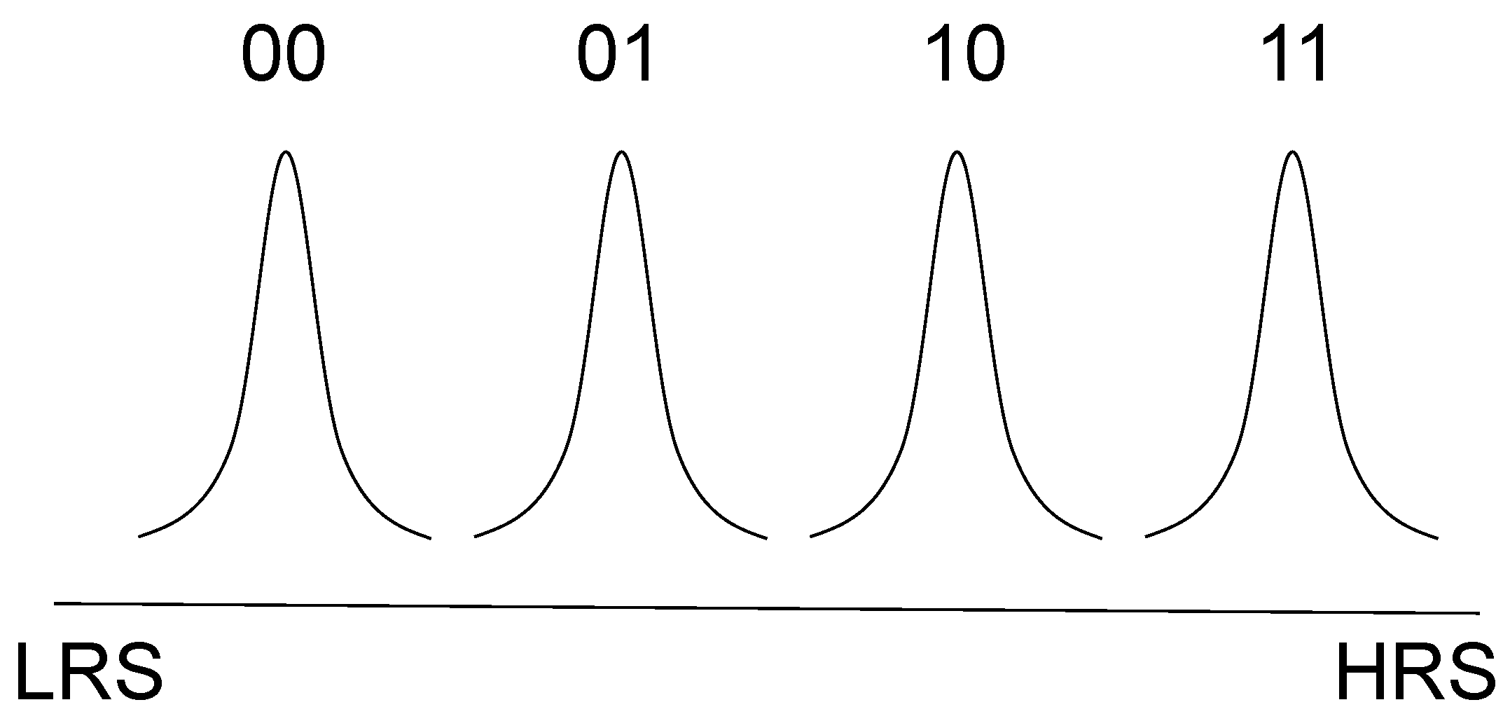
The significant advantage of ReRAM for synapses devices is that they can reduce the physical space of the memory used to express multiple resistances. Multi-level cell (MLC) ReRAM, which stores multiple bits in a single ReRAM cell, can further improve density [50,51,52,53]. Because the resistance is determined by conductive filaments including metal ions and oxygen vacancies, a ReRAM device can express multiple resistances depending upon the voltage polarity and magnitude to create oxygen vacancies and/or metal ions. Figure 6 shows an MLC resistance distribution of a 2-bit example where both a high resistance state (HRS) and a low resistance state (LRS) exist [53,54,55]. Because multiple levels of bit information can be represented as analog values of a single device, it can significantly increase the aggregation compared to DRAMs that use capacitors to represent a single bit or SRAMs that use multiple transistors.
3.3. MRAM: Spintronic Synaptic Devices
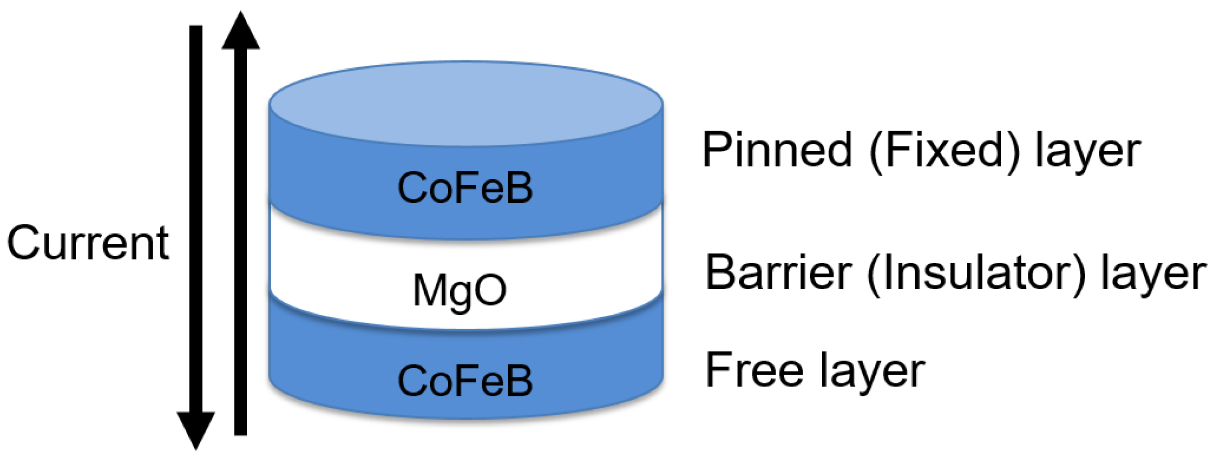
Magnetoresistive random-access memory (MRAM) is a type of non-volatile memory that stores data in the magnetic material. MRAM uses magnetic tunnel junction (MTJ) that consists of two ferromagnetic material layers to store data, a free layer (FL), and a pinned layer (PL) as shown in Figure 7. The spin of an FL can be switched from one orientation to its opposite by applying a current pulse through the MTJ while the spin is set to one orientation in a PL. Each of these spin states exhibits a distinct resistance corresponding to storing a binary ‘0’ and ‘1’ [56,57,58,59].
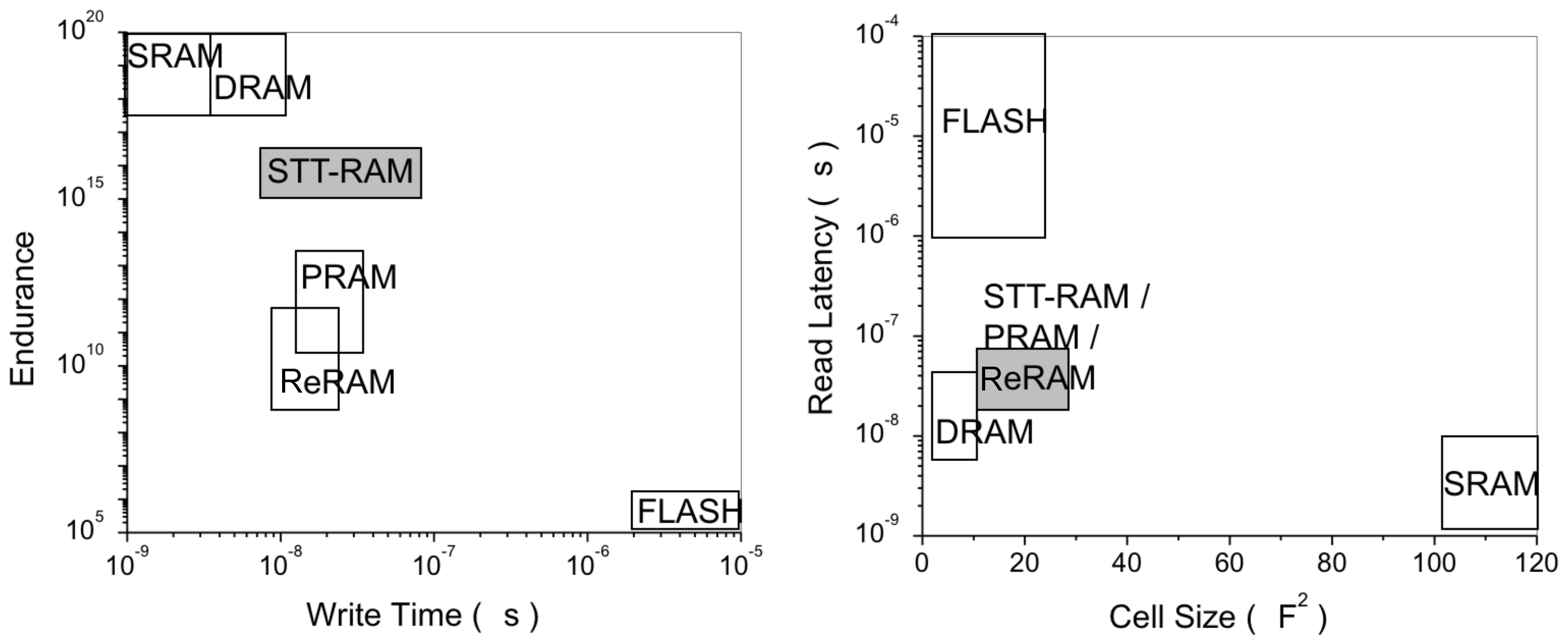
Spin-Transfer Torque RAM (STT-RAM), also called STT-MRAM, is an advanced type of MRAM devices. Because STT-RAM is scalable, this enables higher densities, low power consumption, and reduced cost compared to regular MRAM devices. That is why STT-RAM is currently a majority of MRAM devices. STT-RAM holds significant promise in providing new capabilities and opportunities for low power systems. STT-RAM has been touted as a candidate for a universal memory technology that may be able to provide integration density close to DRAM, the non-volatility of flash memory, fast read speed close to SRAM, and practically zero standby power [57,60,61]. As shown in Figure 8, STT-RAM has higher endurance compared to PRAM and ReRAM because the spintronic device does not use melting or filamenting which impacts material stability.
Moreover, the MRAM device can compute data as well as storing data. This is called Spin logic or Spin-based logic in memory. The spin logic has now attracted significant interest because of its potential that enables the new neuromorphic computing application. This means that the spintronic device can store and compute data like a synapse and a neuron. If one device can mimic both elements of the human brain, that would be efficient. This paper introduces two mainstream of the spin logic. The first approach is to use magnetic devices and additional circuits to perform a logic operation. In [62], a memory array and sense amplifiers with a variable reference are used for logic operations such as AND, OR, and XOR as shown in Figure 9. This design re-utilizes existing memory peripheral circuits to perform logic, arithmetic, and complex vector operations. Depending on the logic such as XOR or OR, the sum of current is compared with a variable reference using a sense amplifier. The current of each bitcell represents a stored value of each bit and the values are examined with the reference. Since the proposed spin logic re-utilizes the existing memory array, this can perform both storing and computing at the same time.
The other approach is to use a new spintronic device that operates a NAND gate operation. A NAND gate is generally classed as a universal gate because the NAND gate can produce any other type of logic gate function. By connecting them in various combinations, all the logic computation can be performed. In [63], a new spin device is proposed that uses an intrinsic property in spin-orbit heterostructures to form a logic gate in which the same magnetic contacts that retain the logic inputs serve to simultaneously perform a logic operation and retain the result. This is in contrast to the structures proposed in [62] which require extra circuits. As shown in Figure 10, two MTJs are placed in series and one channel current can control both MTJs. Depending on input voltage pulses on P and Q nodes, the MTJs’ spin directions are changed at the same time, resulting in two-inputs NAND operation.
STT-RAM holds significant promise in providing new capabilities and opportunities for low power neuromorphic systems as mentioned above. Yet, serious challenges remain for a syntactic device. One of the dominant challenges is the fundamental stochasticity of spin switching operations. The STT write process is inherently stochastic and the actual time to complete a write varies dramatically, with the distribution having a very long tail. This stochasticity of switching time is temporal, leading to variation in transition time even for a single cell. That means that guaranteeing a reliable write is not feasible, resulting in high error. The stochastic switching issue is based on a physical property, so-called thermally activated switching. This stochastic behavior is even more critical compared to PRAM and ReRAM because the temperature is not typically controllable.
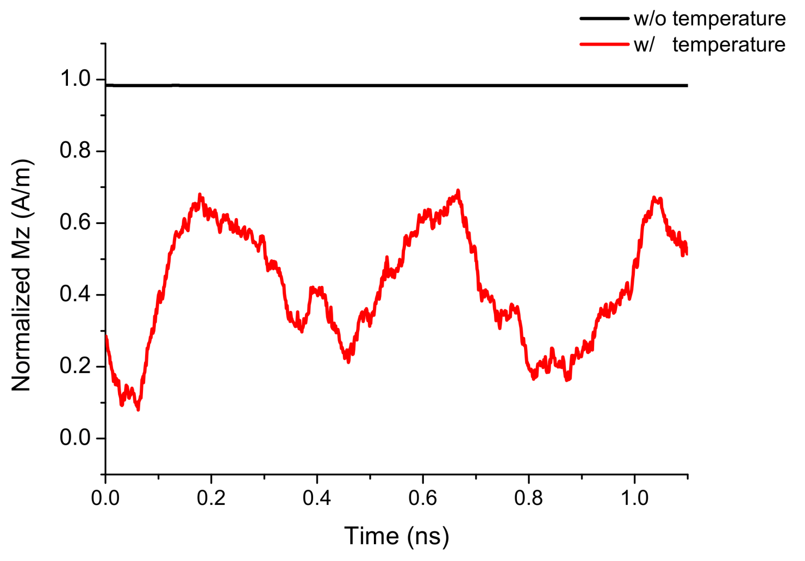
To show and evaluate the stochastic behavior, the detailed magnetic numerical simulator, Object Oriented MicroMagnetic Framework (OOMMF) (Version 1.2, National Institute of Standards and Technology, Gaithersburg, MD, USA) is used [64]. OOMMF is a solver of the Landau–Lifshitz–Gilbert equation [65] describing the magnetization dynamics in a solid. OOMMF is used to simulate the normalized magnetization on the Z-direction (Mz), which represents the macro-spin angle in a free layer, over time. Without temperature, Mz stays constant while Mz shows significant fluctuation with temperature over time as shown in Figure 11. When all spins in a free layer are up, the value of Mz is 1. If all spins are down, the value of Mz is −1. This means the direction of spin stays the same without temperature, but the spin direction varies over time by temperature. This fluctuation induces the switching stochasticity, which is not controllable. This implies eliminating the intrinsic error is not possible even if various circuits and architectures techniques have been proposed to compensate this stochasticity [56,66].
3.4. ASN (Atomic Switch Network): Network-Based Synaptic Device
ASN, sometimes called nanowire networks, is a volatile memristor device that exhibits both short-term and long-term memory behavior [67,68,69,70]. The device can store information as short-term plasticity (STP) with a decay time or long-term potentiation (LTP) if a frequent stimulus exists. This device is typically composed of a network of interfacial atomic switches, which are self-assembled and randomly connected. Ag2S metal-insulator-metal (MIM) interface is widely used to form the switches [71,72]. Silver nanowires or nanoparticles are alternatively used to construct random self-assembled networks in recent researches.
This switch network exhibits a distinct conductance corresponding to storing data by a stimulus, which is voltage in most cases. Once an input voltage is applied to the device, the conductance is changed and sustained for a short time after the voltage is removed. This is called STL and the memory duration varies at random. Under a certain condition, which is most likely breakdown, the conductance is abruptly changed and becomes stable. Repeated input pulses typically produce a continuous and stable conductance pathway, resulting in the final state, called LTP. This device currently focuses on imitating the complex network topology of neurons, rather than stability and controllability. However, this device has a great potential to become the next generation brain-like device because the conductance changes based on its operational history and shows two distinct states, volatile short-term and non-volatile long-term memory behavior like the human brain.
3.5. Approximating Computing Using Emerging Synaptic Devices
New memory devices exhibit entirely new physics-level issues that make older design principles obsolete. This sub-section focuses on an inherent error and design approach based on probabilistic principles to overcome the problem. As mentioned above, the new memory devices induce error due to their physical properties. Specifically, the time needed for the MRAM to switch is stochastic and the distribution is quite wide, resulting in high write error. Furthermore, the resistance’s variation of PRAM and ReRAM introduce error over time. Various circuit- and microarchitecture-level design techniques have developed. However, the additional circuitry introduces non-negligible area and energy overheads.
Instead of reducing the error using such high-cost techniques, this paper suggests adopting Approximate computing. Approximate computing is a computing paradigm that allows inaccurate results to boost other properties such as energy and computing time [73,74,75,76]. Because it is almost impossible to remove the inherent error entirely in the emerging memory devices, it would better to sacrifice the accuracy to maintain low power and small area. Moreover, the goal of machine learning is not expected to have 100% accuracy, but a fast computation with moderate accuracy. Therefore, the approximate computing is suitable for both the machine learning and synaptic devices. The problem needs to be solved and implemented, but at the same time, the solution does not degrade the advantages of the devices. Therefore, the low-cost approximate computing is a promising solution for the error by the emerging devices which is significant across all of the neuromorphic engineering.
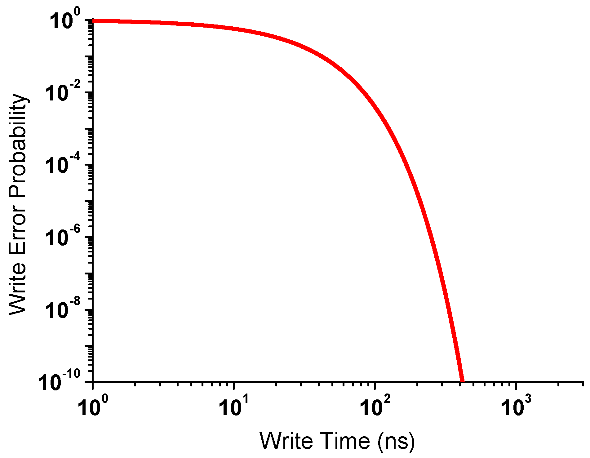
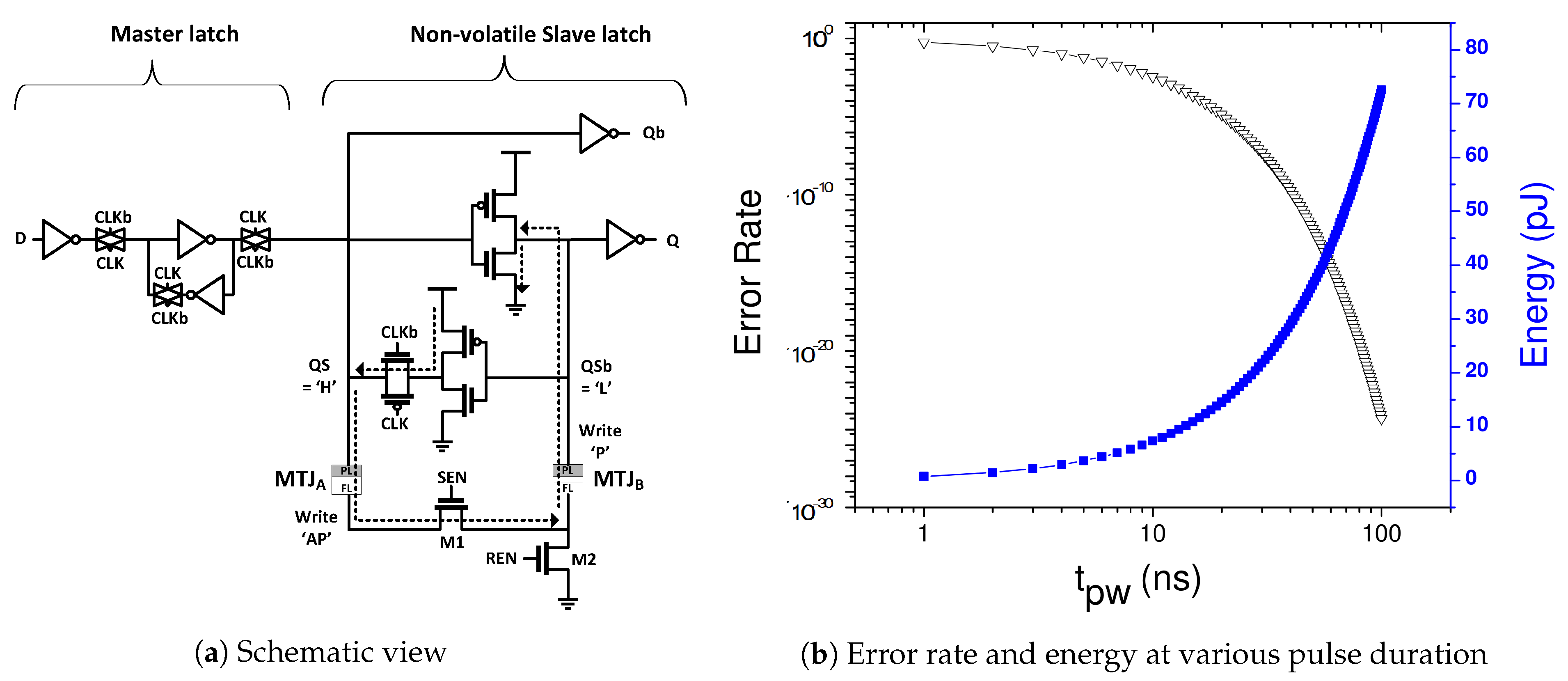
This review introduces an implementation of the approximate computing using a synaptic device. Specifically, an approximate flip-flop using MTJ devices is reviewed [77]. The flip-flop is is a hybrid version of the conventional D flip-flop (D-FF) and non-volatile storage using MTJs for fine-grained power gating. The MTJs are used for temporary storage during power gating. Data on the conventional D flip-flop is stored onto MTJs before the power off and is restored after the power is on again. However, as mentioned in the previous sub-section, the MTJ switching process is inherently stochastic: 100% successful write is not guaranteed. Therefore, the data backed up shows error in any cases. To guarantee a successful write, longer write pulse is typically required as shown in Figure 12. The write error probability is decreased by write pulse (time). However, this approach introduces a significant energy penalty.
Using the approximate computing, the tradeoff between error rate and energy consumption can be resolved effectively. A key insight is that high error rate may be acceptable in some modules of modern hardware systems. In other words, each module has different importance based on its functionally. For example, a flip-flop in a controller is accessed every computation and need to be correct anytime whereas a flip-flop in datapath is only accessed when the data is necessary to be computed. In this case, such data corruption in datapath does not introduce error on outputs. Erroneous data is naturally removed if the data is not accessed for specific computations at various system layers, ranging from circuit- to architectural-level states, called masking effect [78,79]. If we can control error probability of each flop individually, we then would reduce energy effectively.
In [77], the error rate of the flip-flop is easily controlled by changing pulse duration of a control node. Figure 13 shows a schematic view of the flip-flop and an inverse relation between the error rate and energy consumption. Data on the D flip-flop is stored onto MTJs before the power-off (=Storing), and is restored after the power is on again (=Restoring). Consider Q = 1 case. Once SEN signal is turned on, a write current is derived and passed through , M1, and . The is written to the AP state, and becomes the P state because the current direction is reversed. Figure 13b shows the error rate and the expected energy of a flop at various pulse duration, which is controlled by SEN signal. At 6.6 ns, a write error probability is and energy for a storing and restoring operations is 0.2 . For short pulses such as 3.3 ns, the computed error probability is increased to while the energy consumption is reduced by half. Therefore, the error rate of the flip-flop is easily controlled by the pulse duration of a control signal. For the high priority module, the longer pulse duration is needed whereas we could reduce the pulse duration to save energy for the low priority module. This result indicates the approximate computing can maximize the advantage of synaptic devices by saving unnecessary energy while maintaining the required quality of data.
4. Conclusions
Based on Gartner’s projection, the neuromorphic computing market will be expanded from $1.2 billion in 2017 to $15.8 billion in 2022 with a 55% compound annual growth rate (CAGR) [18]. Therefore, researchers need to prepare the new market trend because the neuromorphic computing design is not a plug-and-play method that can be used as soon as a synaptic device is developed. The new computing system requires a design ecosystem with synaptic elements, thus achieving successful joint innovation such as the possibility of developing technologies beyond current semiconductor devices, the establishment of specialized manufacturing processes, and the development of related equipment. Neuromorphic engineering is an area where learning in various fields must be studied together. It is also necessary to understand the learning, memory, and cognitive functions of the brain that are studied in biology, and to incorporate the understanding of computational science.
More importantly, the development of a synaptic device is an essential part. Emerging memory devices are reviewed for neuromorphic computing in this paper. Specifically, PRAM, ReRAM, MRAM, and ASN are discussed as promising candidates for an emerging synaptic device that enables low-power and high integrated neuromorphic systems that will function as a cognitive function that closely mimics the operating principles of the human brain even if there are various existing issues. This paper also suggests implementing an approximate computing concept for the new neuromorphic hardware.
Funding
This research was supported by No. 201901760001 of Handong Global University Research Grants. This work was also supported by Korea Institute for Advancement of Technology (KIAT) grant funded by the Korea Government (MOTIE) (P0008763, The Competency Development Program for Industry Specialist). This work was also supported by the National Program for Excellence in Software at Handong Global University (2017-0-00130) funded by the Ministry of Science and ICT. The EDA tool was supported by the IC Design Education Center (IDEC), Korea.
Conflicts of Interest
The authors declare no conflict of interest.
Abbreviations
The following abbreviations are used in this manuscript:
| AI | artificial Intelligence |
| GPU | graphics processing unit |
| ASIC | application-specific integrated circuit |
| DRAM | dynamic random-access memory |
| SRAM | static random-access memory |
| CMOS | complementary metal–oxide–semiconductor |
| XOR | exclusive OR |
| PRAM | phase-change RAM |
| ReRAM | resistive RAM |
| HRS | high resistance state |
| LRS | low resistance state |
| MRAM | magnetic RAM |
| FL | free layer |
| PL | pinned layer |
| STT-RAM | spin torque transfer RAM |
| MTJ | magnetic tunnel junction |
| CAGR | compound annual growth rate |
References
- Russell, S.; Norvig, P. Artificial Intelligence: A Modern Approach; Prentice Hall: Upper Saddle River, NJ, USA, 2002. [Google Scholar]
- McCorduck, P.; Cfe, C. Machines Who Think: A Personal Inquiry into the History and Prospects of Artificial Intelligence; CRC Press: Boca Raton, FL, USA, 2004. [Google Scholar]
- Jordan, M.I.; Mitchell, T.M. Machine learning: Trends, perspectives, and prospects. Science 2015, 349, 255–260. [Google Scholar] [CrossRef] [PubMed]
- Monroe, D. Neuromorphic Computing Gets Ready for the (Really) Big Time; ACM: New York, NY, USA, 2014. [Google Scholar]
- Poon, C.S.; Zhou, K. Neuromorphic silicon neurons and large-scale neural networks: Challenges and opportunities. Front. Neurosci. 2011, 5, 108. [Google Scholar] [CrossRef] [PubMed] [Green Version]
- Wang, H.; Li, H.; Pino, R.E. Memristor-based synapse design and training scheme for neuromorphic computing architecture. In Proceedings of the 2012 International Joint Conference on Neural Networks (IJCNN), Brisbane, QLD, Australia, 10–15 June 2012; pp. 1–5. [Google Scholar]
- Roy, K.; Jaiswal, A.; Panda, P. Towards spike-based machine intelligence with neuromorphic computing. Nature 2019, 575, 607–617. [Google Scholar] [CrossRef] [PubMed]
- Chi, P.; Li, S.; Xu, C.; Zhang, T.; Zhao, J.; Liu, Y.; Wang, Y.; Xie, Y. Prime: A novel processing-in-memory architecture for neural network computation in reram-based main memory. ACM SIGARCH Comput. Archit. News 2016, 44, 27–39. [Google Scholar] [CrossRef]
- Mahapatra, N.R.; Venkatrao, B. The processor-memory bottleneck: Problems and solutions. XRDS Crossroads ACM Mag. Stud. 1999, 5, 2. [Google Scholar] [CrossRef]
- Sebot, J.; Drach-Temam, N. Memory bandwidth: The true bottleneck of SIMD multimedia performance on a superscalar processor. In European Conference on Parallel Processing; Springer: Berlin/Heidelberg, Germany, 2001; pp. 439–447. [Google Scholar]
- Mead, C. Neuromorphic electronic systems. Proc. IEEE 1990, 78, 1629–1636. [Google Scholar] [CrossRef] [Green Version]
- Douglas, R.; Mahowald, M.; Mead, C. Neuromorphic analogue VLSI. Annu. Rev. Neurosci. 1995, 18, 255–281. [Google Scholar] [CrossRef]
- Zidan, M.A.; Strachan, J.P.; Lu, W.D. The future of electronics based on memristive systems. Nat. Electron. 2018, 1, 22–29. [Google Scholar] [CrossRef]
- Yu, S. Neuro-Inspired Computing Using Resistive Synaptic Devices; Springer: Berlin/Heidelberg, Germany, 2017. [Google Scholar]
- Goldberg, D.H.; Cauwenberghs, G.; Andreou, A.G. Probabilistic synaptic weighting in a reconfigurable network of VLSI integrate-and-fire neurons. Neural Netw. 2001, 14, 781–793. [Google Scholar] [CrossRef] [Green Version]
- Choi, S.; Ham, S.; Wang, G. Memristor synapses for neuromorphic computing. In Memristors-Circuits and Applications of Memristor Devices; IntechOpen: London, UK, 2019. [Google Scholar]
- Camuñas-Mesa, L.A.; Linares-Barranco, B.; Serrano-Gotarredona, T. Neuromorphic Spiking Neural Networks and Their Memristor-CMOS Hardware Implementations. Materials 2019, 12, 2745. [Google Scholar] [CrossRef] [PubMed] [Green Version]
- Priestley, A. Emerging Technology Analysis: Neuromorphic Computing. Nanotechnology 2018, 30, 032001. [Google Scholar]
- Fowers, J.; Ovtcharov, K.; Papamichael, M.; Massengill, T.; Liu, M.; Lo, D.; Alkalay, S.; Haselman, M.; Adams, L.; Ghandi, M.; et al. A configurable cloud-scale DNN processor for real-time AI. In Proceedings of the 2018 ACM/IEEE 45th Annual International Symposium on Computer Architecture (ISCA), Los Angeles, CA, USA, 1–6 June 2018; pp. 1–14. [Google Scholar]
- Ma, D.; Shen, J.; Gu, Z.; Zhang, M.; Zhu, X.; Xu, X.; Xu, Q.; Shen, Y.; Pan, G. Darwin: A neuromorphic hardware co-processor based on spiking neural networks. J. Syst. Archit. 2017, 77, 43–51. [Google Scholar] [CrossRef]
- Jiao, Y.; Han, L.; Jin, R.; Su, Y.J.; Ho, C.; Yin, L.; Li, Y.; Chen, L.; Chen, Z.; Liu, L.; et al. 7.2 A 12nm Programmable Convolution-Efficient Neural-Processing-Unit Chip Achieving 825TOPS. In Proceedings of the 2020 IEEE International Solid-State Circuits Conference-(ISSCC), San Francisco, CA, USA, 16–20 February 2020; pp. 136–140. [Google Scholar]
- Corinto, F.; Civalleri, P.P.; Chua, L.O. A theoretical approach to memristor devices. IEEE J. Emerg. Sel. Top. Circuits Syst. 2015, 5, 123–132. [Google Scholar] [CrossRef] [Green Version]
- Chua, L. Resistance switching memories are memristors. Appl. Phys. A 2011, 102, 765–783. [Google Scholar] [CrossRef] [Green Version]
- Wang, X.; Chen, Y. Spintronic memristor devices and application. In Proceedings of the 2010 Design, Automation & Test in Europe Conference & Exhibition (DATE 2010), Dresden, Germany, 8–12 March 2010; pp. 667–672. [Google Scholar]
- Ho, Y.; Huang, G.M.; Li, P. Nonvolatile memristor memory: Device characteristics and design implications. In Proceedings of the 2009 International Conference on Computer-Aided Design, San Jose, CA, USA, 2–5 November 2009; pp. 485–490. [Google Scholar]
- Chua, L. Memristor-the missing circuit element. IEEE Trans. Circuit Theory 1971, 18, 507–519. [Google Scholar] [CrossRef]
- Suzuki, K.; Swanson, S. A survey of trends in non-volatile memory technologies: 2000–2014. In Proceedings of the 2015 IEEE International Memory Workshop (IMW), Monterey, CA, USA, 17–20 May 2015; pp. 1–4. [Google Scholar]
- Lee, S.H. Scaling trends and challenges of advanced memory technology. In Proceedings of the Technical Program-2014 International Symposium on VLSI Technology, Systems and Application (VLSI-TSA), Hsinchu, Taiwan, 28–30 April 2014; p. 1. [Google Scholar]
- Fujisaki, Y. Current status of nonvolatile semiconductor memory technology. Jpn. J. Appl. Phys. 2010, 49, 100001. [Google Scholar] [CrossRef] [Green Version]
- Sie, C. Memory Devices Using Bistable Resistivity in Amorphous As-Te-Ge Films. Ph.D. Thesis, Iowa State University, Ames, IA, USA, 1969. [Google Scholar]
- Sie, C.; Pohm, A.; Uttecht, P.; Kao, A.; Agrawal, R. Chalcogenide glass bistable resistivity memory. IEEE MAG-6 1970, 6, 592. [Google Scholar]
- Sie, C.; Uttecht, R.; Stevenson, H.; Griener, J.; Raghavan, K. Electricfield induced filament formation in As-Te-Ge glass. J. Non-Cryst. Solids 1970, 2, 358–370. [Google Scholar]
- Ha, D.; Kim, K. Recent advances in high density phase change memory (PRAM). In Proceedings of the 2007 International Symposium on VLSI Technology, Systems and Applications (VLSI-TSA), Hsinchu, Taiwan, 23–25 April 2007; pp. 1–4. [Google Scholar]
- Wong, H.S.P.; Raoux, S.; Kim, S.; Liang, J.; Reifenberg, J.P.; Rajendran, B.; Asheghi, M.; Goodson, K.E. Phase change memory. Proc. IEEE 2010, 98, 2201–2227. [Google Scholar] [CrossRef]
- WAhn, S.; Song, Y.; Jeong, C.; Shin, J.; Fai, Y.; Hwang, Y.; Lee, S.; Ryoo, K.; Lee, S.; Park, J. Highly manufacturable high density phase change memory of 64Mb and beyond. In Proceedings of the IEEE International Electron Devices Meeting, San Francisco, CA, USA, 13–15 December 2004; pp. 907–910. [Google Scholar]
- Suri, M.; Bichler, O.; Querlioz, D.; Cueto, O.; Perniola, L.; Sousa, V.; Vuillaume, D.; Gamrat, C.; DeSalvo, B. Phase change memory as synapse for ultra-dense neuromorphic systems: Application to complex visual pattern extraction. In Proceedings of the 2011 International Electron Devices Meeting, Washington, DC, USA, 5–7 December 2011; p. 4. [Google Scholar]
- Shelby, R.M.; Burr, G.W.; Boybat, I.; Di Nolfo, C. Non-volatile memory as hardware synapse in neuromorphic computing: A first look at reliability issues. In Proceedings of the IEEE International Reliability Physics Symposium, Monterey, CA, USA, 19–23 April 2015; p. 6A-1. [Google Scholar]
- Yu, S. Neuro-inspired computing with emerging nonvolatile memorys. Proc. IEEE 2018, 106, 260–285. [Google Scholar] [CrossRef]
- Suri, M.; Garbin, D.; Bichler, O.; Querlioz, D.; Vuillaume, D.; Gamrat, C.; DeSalvo, B. Impact of PCM resistance-drift in neuromorphic systems and drift-mitigation strategy. In Proceedings of the IEEE/ACM International Symposium on Nanoscale Architectures (NANOARCH), Brooklyn, NY, USA, 15–17 July 2013; pp. 140–145. [Google Scholar]
- Li, J.; Luan, B.; Lam, C. Resistance drift in phase change memory. In Proceedings of the IEEE International Reliability Physics Symposium (IRPS), Anaheim, CA, USA, 15–19 April 2012; p. 6C-1. [Google Scholar]
- Ielmini, D.; Lavizzari, S.; Sharma, D.; Lacaita, A.L. Physical interpretation, modeling and impact on phase change memory (PCM) reliability of resistance drift due to chalcogenide structural relaxation. In Proceedings of the IEEE International Electron Devices Meeting, Washington, DC, USA, 10–12 December 2007; pp. 939–942. [Google Scholar]
- Ielmini, D.; Sharma, D.; Lavizzari, S.; Lacaita, A.L. Reliability impact of chalcogenide-structure relaxation in phase-change memory (PCM) cells—Part I: Experimental study. IEEE Trans. Electron Devices 2009, 56, 1070–1077. [Google Scholar] [CrossRef]
- Boniardi, M.; Ielmini, D. Physical origin of the resistance drift exponent in amorphous phase change materials. Appl. Phys. Lett. 2011, 98, 243506. [Google Scholar] [CrossRef]
- Pirovano, A.; Lacaita, A.L.; Pellizzer, F.; Kostylev, S.A.; Benvenuti, A.; Bez, R. Low-field amorphous state resistance and threshold voltage drift in chalcogenide materials. IEEE Trans. Electron Devices 2004, 51, 714–719. [Google Scholar] [CrossRef]
- Akinaga, H.; Shima, H. Resistive random access memory (ReRAM) based on metal oxides. Proc. IEEE 2010, 98, 2237–2251. [Google Scholar] [CrossRef]
- Yang, J.J.; Strukov, D.B.; Stewart, D.R. Memristive devices for computing. Nat. Nanotechnol. 2013, 8, 13. [Google Scholar] [PubMed]
- Muraoka, S.; Ninomiya, T.; Wei, Z.; Katayama, K.; Yasuhara, R.; Takagi, T. Comprehensive understanding of conductive filament characteristics and retention properties for highly reliable ReRAM. In Proceedings of the 2013 Symposium on VLSI Technology, Kyoto, Japan, 11–13 June 2013. [Google Scholar]
- Wei, Z.; Eriguchi, K. Analytic modeling for nanoscale resistive filament variation in ReRAM with stochastic differential equation. IEEE Trans. Electron Devices 2017, 64, 2201–2206. [Google Scholar] [CrossRef]
- Liu, Q.; Long, S.; Lv, H.; Wang, W.; Niu, J.; Huo, Z.; Chen, J.; Liu, M. Controllable growth of nanoscale conductive filaments in solid-electrolyte-based ReRAM by using a metal nanocrystal covered bottom electrode. ACS Nano 2010, 4, 6162–6168. [Google Scholar] [CrossRef]
- Kang, J.; Li, H.; Huang, P.; Chen, Z.; Gao, B.; Liu, X.; Jiang, Z.; Wong, H. Modeling and design optimization of ReRAM. In Proceedings of the 20th Asia and South Pacific Design Automation Conference, Tokyo, Japan, 19 January–22 January 2015; pp. 576–581. [Google Scholar]
- Bai, Y.; Wu, H.; Wu, R.; Zhang, Y.; Deng, N.; Yu, Z.; Qian, H. Study of Multi-level Characteristics for 3D Vertical Resistive Switching Memory. Sci. Rep. 2014, 4. [Google Scholar] [CrossRef] [Green Version]
- Xu, C.; Niu, D.; Muralimanohar, N.; Jouppi, N.P.; Xie, Y. Understanding the trade-offs in multi-level cell ReRAM memory design. In Proceedings of the 50th ACM/EDAC/IEEE Design Automation Conference (DAC), Austin, TX, USA, 29 May–7 June 2013; pp. 1–6. [Google Scholar]
- Ramadan, M.; Wainstein, N.; Ginosar, R.; Kvatinsky, S. Adaptive programming in multi-level cell ReRAM. Microelectron. J. 2019, 90, 169–180. [Google Scholar] [CrossRef]
- Niu, D.; Zou, Q.; Xu, C.; Xie, Y. Low power multi-level-cell resistive memory design with incomplete data mapping. In Proceedings of the 2013 IEEE 31st International Conference on Computer Design (ICCD), Asheville, NC, USA, 6–9 October 2013; pp. 131–137. [Google Scholar]
- Puglisi, F.M.; Larcher, L.; Bersuker, G.; Padovani, A.; Pavan, P. An empirical model for RRAM resistance in low-and high-resistance states. IEEE Electron Device Lett. 2013, 34, 387–389. [Google Scholar] [CrossRef]
- Park, J.; Zheng, T.; Erez, M.; Orshansky, M. Variation-Tolerant Write Completion Circuit for Variable-Energy Write STT-RAM Architecture. IEEE Trans. Large Scale Integr. (VLSI) Syst. 2016, 24, 1351–1360. [Google Scholar] [CrossRef]
- Nigam, A.; Smullen, C.W.; Mohan, V.; Chen, E.; Gurumurthi, S.; Stan, M.R. Delivering on the promise of universal memory for spin-transfer torque RAM (STT-RAM). In Proceedings of the IEEE/ACM International Symposium on Low Power Electronics and Design, Fukuoka, Japan, 1–3 August 2011; pp. 121–126. [Google Scholar]
- Hong, S.; Auciello, O.; Wouters, D. Emerging Non-Volatile Memories; Springer: Berlin/Heidelberg, Germany, 2014. [Google Scholar]
- Dong, X.; Wu, X.; Sun, G.; Xie, Y.; Li, H.; Chen, Y. Circuit and microarchitecture evaluation of 3D stacking magnetic RAM (MRAM) as a universal memory replacement. In Proceedings of the 45th ACM/IEEE Design Automation Conference, Anaheim, CA, USA, 8–13 June 2008; pp. 554–559. [Google Scholar]
- Freitas, R.F.; Wilcke, W.W. Storage-class memory: The next storage system technology. IBM J. Res. Dev. 2008, 52, 439–447. [Google Scholar] [CrossRef]
- Kim, W.; Jeong, J.; Kim, Y.; Lim, W.; Kim, J.; Park, J.; Shin, H.; Park, Y.; Kim, K.; Park, S.; et al. Extended scalability of perpendicular STT-MRAM towards sub-20nm MTJ node. In Proceedings of the 2011 International Electron Devices Meeting, Washington, DC, USA, 5–7 December 2011; p. 24. [Google Scholar]
- Jain, S.; Ranjan, A.; Roy, K.; Raghunathan, A. Computing in Memory With Spin-Transfer Torque Magnetic RAM. IEEE Trans. Large Scale Integr. (VLSI) Syst. 2018, 26, 470–483. [Google Scholar] [CrossRef]
- Kazemi, M. An electrically reconfigurable logic gate intrinsically enabled by spin-orbit materials. Sci. Rep. 2017, 7. [Google Scholar] [CrossRef] [Green Version]
- Donahue, M.; Porter, D. OOMMF User Guide, Version 1.0; Interagency Report NISTIR 6376; National Institute of Standard and Technology: Gaithersburg, MD, USA, 1999. Available online: http://math.nist.gov/oommf (accessed on 10 May 2020).
- Gilbert, T. Anomalous rotational damping in ferromagnetic sheets. In Proceedings of the Conference on Magnetism and Magnetic Materials, Pittsburgh, PA, USA, 14–16 June 1955. [Google Scholar]
- Park, J.; Yim, Y.U. Two-Phase Read Strategy for Low Energy Variation-Tolerant STT-RAM. IEEE Trans. Large Scale Integr. (VLSI) Syst. 2018, 26, 2584–2590. [Google Scholar] [CrossRef]
- Ohno, T.; Hasegawa, T.; Tsuruoka, T.; Terabe, K.; Gimzewski, J.K.; Aono, M. Short-term plasticity and long-term potentiation mimicked in single inorganic synapses. Nat. Mater. 2011, 10, 591–595. [Google Scholar] [CrossRef]
- Manning, H.G.; Niosi, F.; da Rocha, C.G.; Bellew, A.T.; O’Callaghan, C.; Biswas, S.; Flowers, P.F.; Wiley, B.J.; Holmes, J.D.; Ferreira, M.S.; et al. Emergence of winner-takes-all connectivity paths in random nanowire networks. Nat. Commun. 2018, 9, 1–9. [Google Scholar] [CrossRef]
- Du, C.; Cai, F.; Zidan, M.A.; Ma, W.; Lee, S.H.; Lu, W.D. Reservoir computing using dynamic memristors for temporal information processing. Nat. Commun. 2017, 8, 1–10. [Google Scholar] [CrossRef]
- Bose, S.; Shirai, S.; Mallinson, J.; Brown, S. Synaptic dynamics in complex self-assembled nanoparticle networks. Faraday Discuss. 2019, 213, 471–485. [Google Scholar] [CrossRef] [Green Version]
- Diaz-Alvarez, A.; Higuchi, R.; Sanz-Leon, P.; Marcus, I.; Shingaya, Y.; Stieg, A.Z.; Gimzewski, J.K.; Kuncic, Z.; Nakayama, T. Emergent dynamics of neuromorphic nanowire networks. Sci. Rep. 2019, 9, 1–13. [Google Scholar] [CrossRef] [Green Version]
- Stieg, A.Z.; Avizienis, A.V.; Sillin, H.O.; Martin-Olmos, C.; Aono, M.; Gimzewski, J.K. Emergent criticality in complex turing B-type atomic switch networks. Adv. Mater. 2012, 24, 286–293. [Google Scholar] [CrossRef] [PubMed]
- Mittal, S. A Survey of Techniques for Approximate Computing. ACM Comput. Surv. 2016, 48, 1–33. [Google Scholar] [CrossRef] [Green Version]
- Sampson, A.; Nelson, J.; Strauss, K.; Ceze, L. Approximate storage in solid-state memories. In Proceedings of the 46th Annual IEEE/ACM International Symposium on Microarchitecture (MICRO), Davis, CA, USA, 7–11 December 2013; pp. 25–36. [Google Scholar]
- Han, J.; Orshansky, M. Approximate computing: An emerging paradigm for energy-efficient design. In Proceedings of the 18th IEEE European Test Symposium (ETS), Avignon, France, 27–30 May 2013; pp. 1–6. [Google Scholar]
- Akturk, I.; Khatamifard, K.; Karpuzcu, U.R. On quantification of accuracy loss in approximate computing. In Proceedings of the Workshop on Duplicating, Deconstructing and Debunking (WDDD), Portland, PA, USA, 14 June 2015; Volume 15. [Google Scholar]
- Park, J.; Yim, Y.U. Fine-Grained Power Gating Using an MRAM-CMOS Non-Volatile Flip-Flop. Micromachines 2019, 10, 411. [Google Scholar] [CrossRef] [PubMed] [Green Version]
- Paliaroutis, G.I.; Tsoumanis, P.; Evmorfopoulos, N.; Dimitriou, G.; Stamoulis, G.I. Set Pulse Characterization and SER Estimation in Combinational Logic with Placement and Multiple Transient Faults Considerations. Technologies 2020, 8, 5. [Google Scholar] [CrossRef] [Green Version]
- Jang, S.; Park, J. HYFII: HYbrid Fault Injection Infrastructure for Accurate Runtime System Failure Analysis. IEEE Trans. Large Scale Integr. (VLSI) Syst. 2020. [Google Scholar] [CrossRef]
Figure 1.
A neural network of the human brain.

Figure 2.
Block diagram of computing systems: (a) von Neumann architecture; (b) neuromorphic architecture.
Figure 2.
Block diagram of computing systems: (a) von Neumann architecture; (b) neuromorphic architecture.

Figure 3.
Evolution of the neuromorphic hardware.

Figure 4.
A PRAM device design that has phase change material.

Figure 5.
A ReRAM structure and its Set and Reset operations.

Figure 6.
An MLC resistance distribution.

Figure 7.
Block diagram of a perpendicular MTJ.

Figure 8.
Performance comparison of memory devices.

Figure 9.
Block diagram of a memory array and sense amplifiers with a variable reference to perform a logic function.
Figure 9.
Block diagram of a memory array and sense amplifiers with a variable reference to perform a logic function.

Figure 10.
A spin logic device with two MTJs [63].
Figure 10.
A spin logic device with two MTJs [63].

Figure 11.
Magnetization on Z-direction (Mz) over time obtained via numerical simulations.

Figure 12.
Write error probability of a MTJ at various write times.

Figure 13.
An approximate non-volatile flip-flop proposed in [77].
Figure 13.
An approximate non-volatile flip-flop proposed in [77].

© 2020 by the author. Licensee MDPI, Basel, Switzerland. This article is an open access article distributed under the terms and conditions of the Creative Commons Attribution (CC BY) license (http://creativecommons.org/licenses/by/4.0/).
Share and Cite
MDPI and ACS Style
Park, J. Neuromorphic Computing Using Emerging Synaptic Devices: A Retrospective Summary and an Outlook. Electronics 2020, 9, 1414. https://0-doi-org.brum.beds.ac.uk/10.3390/electronics9091414
AMA Style
Park J. Neuromorphic Computing Using Emerging Synaptic Devices: A Retrospective Summary and an Outlook. Electronics. 2020; 9(9):1414. https://0-doi-org.brum.beds.ac.uk/10.3390/electronics9091414
Chicago/Turabian StylePark, Jaeyoung. 2020. "Neuromorphic Computing Using Emerging Synaptic Devices: A Retrospective Summary and an Outlook" Electronics 9, no. 9: 1414. https://0-doi-org.brum.beds.ac.uk/10.3390/electronics9091414
Note that from the first issue of 2016, this journal uses article numbers instead of page numbers. See further details here.