A New Read Scheme for Alleviating Cell-to-Cell Interference in Scaled-Down 3D NAND Flash Memory


1
Department of Electronics Engineering, Hanyang University, Seoul 04763, Korea
2
Department of Electronics Engineering, Korea National University of Transportation, Chung-ju 27469, Korea
*
Author to whom correspondence should be addressed.
Electronics 2020, 9(11), 1775; https://0-doi-org.brum.beds.ac.uk/10.3390/electronics9111775
Submission received: 7 October 2020
/
Revised: 23 October 2020
/
Accepted: 24 October 2020
/
Published: 26 October 2020
(This article belongs to the Special Issue New CMOS Devices and Their Applications)
Abstract
:In this paper, we investigated the cell-to-cell interference in scaled-down 3D NAND flash memory by using a Technology Computer-Aided Design (TCAD) simulation. The fundamental cause of cell-to-cell interference is that the electric field crowding point is changed by the programmed adjacent cell so that the electric field is not sufficiently directed to the channel surface. Therefore, the channel concentration of the selected cell is changed, leading to a Vth shift. Furthermore, this phenomenon occurs more severely when the selected cell is in an erased state rather than in a programmed state. In addition, it was confirmed that the cell-to-cell interference by the programmed WLn+1 is more severe than that of WLn−1 due to the degradation of the effective mobility effect. To solve this fundamental problem, a new read scheme is proposed. Through TCAD simulation, the cell-to-cell interference was alleviated with a bias having a ΔV of 1.5 V from Vread through an optimization process to have appropriate bias conditions in three ways that are suitable for each pattern. As a result, this scheme narrowed the Vth shift of 67.5% for erased cells and narrowed the Vth shift of 70% for programmed cells. The proposed scheme is one way to solve the cell-to-cell interference that may occur as the cell-to-cell distance decreases for a high stacked 3D NAND structure.
1. Introduction
Since the release of the 3D NAND flash product for the first time in 2014 [1], the bit density could be increased rapidly by increasing the number of WL (Word line) stacking layers, which starts at 24, came up to 128 [1,2,3,4,5,6], and it is unpredictable how many it will increase to fulfill the explosive growth of data demand. In this situation, while increasing the number of stacked WL layers, the mold stacking height should be scaled down due to the limitations of the channel hole etching process. However, if the gate and space length are reduced through the height being scaled down, the memory characteristics change, and it leads to reliability issues [7,8,9,10,11,12,13,14]. One of the issues is due to the junction-less poly silicon channel of 3D NAND structure. In effect, the channel of the main cells is based on the ultra-thin body (UTB) structure, which is not connected to the substrate [15,16]. Therefore, during the read operation, the selected cell is affected by the Vread (read voltage) of the adjacent cell, which leads to cell-to-cell interference [11,12,17]. Since the cell-to-cell interference is different from the conventional FG (floating gate) of a planar 2D NAND structure [18,19,20], research on the cell-to-cell interference in 3D NAND has not been investigated yet. Therefore, in this paper, when scaled down in a 3D NAND structure, cell-to-cell interference according to each pattern was studied using TCAD simulation (Synopsys SentaurusTM). This is not only to investigate the interference according to the bias condition of the adjacent cells but also to consider the program state of all cells in the NAND string. After that, we proposed a new read scheme using a local bias condition that can alleviate the cell-to-cell interference.
2. Simulation Set-Up
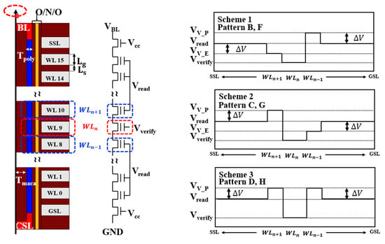
In this paper, TCAD simulation was performed to analyze the cell-to-cell interference of 3D NAND flash memory. The 3D structure used is shown in Figure 1a. The NAND string is a 16-layer structure, in which a BL (Bit-Line), SSL (String Select Line), GSL (Ground Select Line), and CSL (Common Source Line) are constructed. Typically, both the gate and space lengths are scaled down at the same time in 3D NAND flash memory. However, in this simulation, the gate length was set equal to 30 nm for all structures, and the space length was reduced by 5 nm from 30 nm and scaled down to 10 nm. The reason for this setting is if the gate length is changed, a difference in both the gate controllability and the charge trap density occurs. We set WL9 as a selected cell of the read operation and confirmed cell-to-cell interference using the states of adjacent cells WLn−1 and WLn+1. Figure 1b is the equivalent circuit and bias conditions to read through a 3D NAND string. Figure 1c is the pulse diagram of the program and read operation. The program voltage is 20 V and the pass voltage is 6 V with 3.3 V applied to the SSL in the selected bit line. The read voltage is 6 V with 3.3 V applied to the SSL/GSL. The selected cell bias is swept from −5 V to 5 V to verify the cell state and the BL voltage is set to 1 V. The list in Table 1 shows patterns for investigating interference in selected cells (WLn) according to the state of the adjacent cell. We have listed all patterns for three cells. Patterns A, B, C, and D are used to identify interference when the selected cell is in the erased state, and the patterns E, F, G, and H are configured to identify interference when the selected cell is in the programmed state. Lastly, in the TCAD simulation, the physics model in poly-silicon used a doping dependence model and high-field saturation model for mobility. Furthermore, the recombination model used the doping dependence of the SRH (Shockley–Read–Hall) lifetime model, respectively. In addition, the poly-silicon channel is affected by the GBT (Grain Boundary Trap) for memory operation [21]. In this simulation, we excluded this effect to avoid complexity and only considering the cell-to-cell distance effect.
3. Cell-To-Cell Interference
Figure 2 shows the Vth shift caused by cell-to-cell interference with scaled down in 3D NAND flash memory according to each pattern. As the space length decreases, it can be seen that the interference increases regardless of the pattern type. However, the interference is more severe than the programmed state when the selected cell is in the erased state. In addition, patterns D and H, where WLn+1 and WLn−1 are programmed, have the most serious cell-to-cell interference; however, we should note that the interference caused by programmed WLn+1 is more severe than that of WLn−1.
First, the cell-to-cell interference caused by the reduction in the space length was examined through the process of changing the state from pattern A to B, and E and F. Figure 3a,b show the conduction band at the channel surface when the selected cell is turned on (Vverify = Vth of selected cell) in the read operation. In Figure 3a, which has both gate and space length and a 30 nm structure, it can be confirmed that the conduction band at pattern B is relatively higher than that of pattern A at the WLn−1 channel region despite the Vread bias. This acts as a source resistance during the read operation, but the interference is considered negligible because there is no change in the conduction band in the selected cell channel region nearby. In the case of patterns E and F, there is no change in the conduction band.
However, the space length is scaled down to 10 nm in the 3D NAND structure in Figure 3b; when the read operation is changed from pattern A to B, the raised conduction band of the programmed WLn−1 overlaps the selected cell channel area. As a result, the conduction band distortion occurs. Finally, when comparing the conduction bands of patterns E and F in a 10 nm length structure, it was found that the distortion is relatively negligible compared with patterns A and B.
To examine these causes in detail, Figure 4 confirmed the electron density at the channel area during the read operation at each pattern. Figure 4a,b shows the electron density contour according to the pattern in the space length, which is 30 nm when the selected cell is turned on during the read operation. As WLn−1 was programmed as the pattern changed from A to B, the electron density of the inversion layer by Vread was lower than that of pattern A. However, it does not affect the channel area of the selected cell. This is because it maintains a strong inversion state nearby the selected cell. As a result, the verify voltage in Figure 4b is −0.761, which is as high as 0.067 V than Figure 4a. Likewise, in Figure 4c,d, when the space length is 10 nm, the electron concentration contour changing from pattern A to B can be confirmed. Compared with Figure 4a,b, and since the space length is shortened to 10 nm, Figure 4d shows that the insufficient electron concentration in the WLn−1 channel region overlaps the channel concentration of the selected cell. As a result, it maintains the light inversion state at a nearby selected cell. Therefore, the verify voltage in Figure 4d is −1.860, which is as high as 0.279 V in Figure 4c. Lastly, in Figure 5e,f, when the space length is 10 nm, the electron concentration contour changing from pattern E to F can be confirmed. As in Figure 4b, it can be confirmed that the electron concentration of the selected cell is not affected due to the strong inversion. As a result, the verify voltage in Figure 5f is 2.540, which is as high as 0.04 V compared with Figure 5e. Therefore, if the space length is short enough, cell-to-cell interference is negligible in the programmed selected cell.
Specifically, to investigate the difference of electron concentration at each state, Figure 5a shows the electric field contour and direction generated during the read operation. The electric field crowding point occurs near the nitride trap layer of the WLn−1 due to the trapped electron charge and near the selected cell gate region due to the low verify voltage compared to the read voltage. As a result, the electric field generated through the Vread voltage applied to WLn−1 is directed to the crowding point, but the fringe field can bypass the channel region through sufficient space length; as a result, it can be confirmed that the electric field is directed to the channel surface leading to strong inversion nearby the selected cell, as shown in Figure 4b However, as shown in Figure 5b, when the space length is short, there is no distance that the electric field can bypass. So, it can be confirmed that the electric field is not directed to the channel region leading to light inversion as shown in Figure 4d. Finally, Figure 5c shows the electric field in Figure 4f. Compared to Figure 5b, the verify voltage increased due to the programmed state; therefore, the electric field crowding point was changed from the gate to the nitride trap layer. As a result, the fringe field can reach the channel surface region, leading to strong inversion.
In conclusion, due to the difference in field direction, a difference in electron concentration in the channel surface region occurs. Through the cell-to-cell interference due to the change from pattern A to B and E to F, we confirmed that the interference with WLn−1 is the inability to form a junction due to an insufficient electric field.
However, as shown in Figure 3, the cell-to-cell interference due to the change from pattern A to C and E to G is more severe. Figure 6d shows all the conduction bands at the channel surface in patterns A, B, C, and D at a space length of 10 nm in the 3D NAND Structure during the read operation.
The conduction band is significantly increased by the programmed WLn+1 compared with the programmed WLn−1. The conduction band slope between WLn+1 and WLn becomes smooth, leading to conduction band distortion. Through this point, cell-to-cell interference from pattern C is more severe than pattern B. and this conduction band distortion effect inferred a significant drop in the electric field.
In effect, during the read operation, drift current occurs through the Vbl and Vread, but the electric field due to Vread is weakened by the programmed WLn+1. Therefore, as shown in Figure 6a, while in the gate and space length of a 30 nm structure, there is no change in effective mobility in patterns C and D because sufficient fringe fields by Vread are directed to the space region, when the space length is 10 nm as shown in Figure 6b, effective mobility is significantly degraded because the fringe field could not be directed to the channel surface. Therefore, as shown in Figure 6c, due to this mobility degradation, electrons flowing through the field over the channel increase SRH recombination, leading to lowering the channel concentration and more severe cell-to-cell interference than programmed WLn−1 induced interference.
Lastly, in simple terms, pattern D has the greatest interference because it affects both WLn−1 and WLn+1 interference. As for the patterns E, F, G, and H, which is the interference of the programmed selected cell, the fringe field is directed near the channel surface, as shown in Figure 4c; so, it is relatively lower than the interference shown in patterns A, B, C, and D.
In order to alleviate this interference, it is necessary to resolve the insufficient field on a local bias in the read operation. Therefore, in the next section, we describe the proposed method to solve this.
4. Proposed Read Scheme
To summarize the above, we have compared and analyzed the interference phenomenon for all patterns of one selected cell and two adjacent cells in a scaled-down 3D NAND flash memory. The fundamental reason for the cell-to-cell interference is that the electron concentration changes by the fringe field to the channel surface area near the selected cell.
Therefore, we proposed to alleviate the cell-to-cell interference by controlling the Vread bias condition of adjacent cells. Figure 7a–c shows the word line bias schemes 1, 2, and 3 to alleviate the field degradation with each pattern. Figure 7a tries to alleviate the cell-to-cell interference due to electric field degradation by applying VV_P bias, which is higher by ∆V than Vread in the case of patterns B and F. Likewise, in Figure 7b, to alleviate the mobility degradation in pattern C and G, as shown in Figure 6b, it is also intended to alleviate the cell-to-cell interference through VV_P bias. However, for the simplification of the scheme, if patterns A and E are read through schemes 1 or 2, the Vth shift is minimized through VV_E, which is lower by ∆V than Vread, to compensate for the increased electron concentration at channel surface by VV_P. So, schemes 1 and 2 attempt to solve patterns A, B, C, E, F, and G through asymmetric read operation through VV_P and VV_E. For patterns D and H, scheme 3 as shown in Figure 7c is used to alleviate electric field degradation through VV_P bias. However, if the ∆V in scheme 3 is too high, a short channel effect may occur [11]. Therefore, the VV_P bias increase should not be too large.
Schemes 1, 2, and 3 can alleviate the cell-to-cell interference for each pattern, but all schemes have different Vth values for ∆V, one ∆V must be set that satisfies for all patterns.
Figure 7d shows the Vth for each pattern according to ∆V. As mentioned above, for simplicity of the scheme, patterns A and E will perform a read operation using schemes 1 or 2, but the scheme closest to Vth of the other patterns will be selected. As a result, in Figure 7d, the point where the patterns A, B, C, and D are gathered is 2 V of ∆V. In pattern A, scheme 1 was closer to the Vth values of all patterns than scheme 2. In addition, in Figure 7e, the Vth values of all the patterns are adjacent at the point where the ∆V was 1. Furthermore, pattern E is more adjacent to the Vth values of all the patterns of Scheme 1 than Scheme 2. Therefore, it is judged that ∆V is compatible with 1.5 in all patterns.
Figure 8 shows the result of the I-V curve characteristic curve of the selected cell for each pattern through TACD simulation using the conventional and proposed read scheme with a ∆V of 1.5 V in a 3D NAND flash memory structure with a gate length of 30 nm and a space length of 10 nm. When comparing Figure 8a,c, the Vth shift range was 0.914 V in a conventional read scheme, but it decreased by approximately 67.5% to 0.297 V through the proposed read scheme, and when comparing Figure 8 b,d, the Vth shift range was reduced by approximately 70.7% to 0.571 V in the conventional scheme and 0.167 V in the proposed scheme. In addition, it can be seen that the reduction rate of the BL current of the proposed scheme is smaller than that of the conventional scheme. Therefore, the proposed scheme can minimize cell-to-cell interference when the space length is reduced by scaled-down in 3D NAND flash memory.
5. Conclusions
In this paper, we analyzed the cell-to-cell interference that occurs as the space length decreases. When the adjacent cells were programmed, the Vread bias during the read operation affects the channel concentration of the selected cell region due to the insufficient bias condition of the electric field to the channel surface. To solve the cell-to-cell interference caused by the electric field, it is necessary to optimize the bias for adjacent cells, which have the most influence on the channel concentration of the selected cell, in each pattern during the read operation.
Therefore, the proposed read scheme was able to alleviate the Vth shift of the selected cells by the program of the adjacent cells by changing the ∆V of 1.5 V in the Vread bias applied to the adjacent cells according to each pattern. In a high-stacking structure, such a cell-to-cell interference issue cannot be avoided. Therefore, if the gate and space length are further scaled down and the cell-to-cell interference is severe, through the string patterning and read operation using the proposed scheme, it will be able to alleviate the interference problem.
Author Contributions
Methodology, paper writing, investigation, conceptualization, Validation, writing, investigation, J.-M.S. Review, M.K. Funding acquisition, supervision, editing, Y.-H.S. All authors have read and agreed to the published version of the manuscript.
Funding
This research was supported by the Ministry of Trade, Industry & Energy (MOTIE (project number 20003808)) and Korea Semiconductor Research Consortium (KSRC) support program for the development of the future semiconductor device. Also, the EDA tool was supported by the IC Design Education Center (IDEC), Korea.
Conflicts of Interest
The authors declare no conflict of interest.
References
- Park, K.T.; Nam, S.; Kim, D.; Kwak, P.; Lee, D.; Choi, Y.H.; Choi, M.H.; Kwak, D.H.; Kim, M.S.; Park, H.W.; et al. Three-Dimensional 128 Gb MLC Vertical nand Flash Memory with 24-WL Stacked Layers and 50 MB/s High-Speed Programming. IEEE J. Solid-State Circuits 2015, 50, 204–213. [Google Scholar] [CrossRef]
- Jeong, W.; Im, J.W.; Kim, D.H.; Nam, S.W.; Shim, D.K.; Choi, M.H.; Yoon, H.J.; Kim, D.H.; Kim, Y.S.; Park, H.W.; et al. A 128 Gb 3b/cell V-NAND Flash Memory with 1 Gb/s I/O Rate. IEEE J. Solid-State Circuits 2016, 51, 204–212. [Google Scholar] [CrossRef]
- Kang, D.; Jeong, W.; Kim, C.; Kim, D.H.; Cho, Y.S.; Kang, K.T.; Ryu, J.; Kang, K.M.; Lee, S.; Kim, W.; et al. 256 Gb 3 b/Cell V-nand Flash Memory with 48 Stacked WL Layers. IEEE J. Solid-State Circuits 2017, 52, 210–217. [Google Scholar] [CrossRef]
- Kim, C.; Kim, D.H.; Jeong, W.; Kim, H.J.; Park, I.H.; Park, H.W.; Lee, J.H.; Park, J.Y.; Ahn, Y.L.; Lee, J.Y.; et al. A 512-Gb 3-b/Cell 64-Stacked WL 3-D-NAND Flash Memory. IEEE J. Solid-State Circuits 2018, 53, 124–133. [Google Scholar] [CrossRef]
- Kang, D.; Kim, M.; Jeon, S.C.; Jung, W.; Park, J.; Choo, G.; Shim, D.K.; Kavala, A.; Kim, S.B.; Kang, K.M.; et al. 13.4 A 512Gb 3-bit/Cell 3D 6th-Generation V-NAND Flash Memory with 82MB/s Write Throughput and 1.2Gb/s Interface. In Proceedings of the 2019 IEEE International Solid- State Circuits Conference—(ISSCC), San Francisco, CA, USA, 17–21 February 2019; pp. 216–218. [Google Scholar] [CrossRef]
- Siau, C.; Kim, K.H.; Lee, S.; Isobe, K.; Shibata, N.; Verma, K.; Ariki, T.; Li, J.; Yuh, K.; Amarnath, A.; et al. 13.5 A 512Gb 3-bit/Cell 3D Flash Memory on 128-Wordline-Layer with 132MB/s Write Performance Featuring Circuit-Under-Array Technology. In Proceedings of the 2019 IEEE International Solid- State Circuits Conference—(ISSCC), San Francisco, CA, USA, 17–21 February 2019; pp. 218–220. [Google Scholar] [CrossRef]
- Jia, X.; Jin, L.; Hou, W.; Wang, Z.; Jiang, S.; Li, K.; Huang, D.; Liu, H.; Wei, W.; Lu, J.; et al. Impact of Cycling Induced Intercell Trapped Charge on Retention Charge Loss in 3-D NAND Flash Memory. IEEE J. Electron Devices Soc. 2020, 8, 62–66. [Google Scholar] [CrossRef]
- Maconi, A.; Arreghini, A.; Compagnoni, C.M.; Van den bosch, G.; Spinelli, A.S.; Van Houdt, J.; Lacaita, A.L. Impact of lateral charge migration on the retention performance of planar and 3D SONOS devices. In Proceedings of the European Solid-State Device Research Conference (ESSDERC), Helsinki, Finland, 12–16 September 2011; pp. 195–198. [Google Scholar] [CrossRef]
- Compagnoni, C.M.; Spinelli, A.S. Reliability of NAND Flash Arrays: A Review of What the 2-D–to–3-D Transition Meant. IEEE Trans. Electron Devices 2019, 66, 4504–4516. [Google Scholar] [CrossRef]
- Goda, A. 3-D NAND Technology Achievements and Future Scaling Perspectives. IEEE Trans. Electron Devices 2020, 67, 1373–1381. [Google Scholar] [CrossRef]
- Hsiao, Y.H.; Lue, H.T.; Chen, W.C.; Chang, K.P.; Tsui, B.Y.; Hsieh, K.Y.; Lu, C.Y. Impact of Vpass Interference on Charge-Trapping NAND Flash Memory Devices. IEEE Trans. Device Mater. Reliab. 2015, 15, 136–141. [Google Scholar] [CrossRef]
- Chen, W.C.; Lue, H.T.; Hsieh, C.C.; Lee, Y.C.; Du, P.Y.; Hsu, T.H.; Chang, K.P.; Wang, K.C.; Lu, C.Y. A physics-based Quasi-2D model to understand the Word line (WL) interference effects of junction-free structure of 3D NAND and experimental study in a 3D NAND flash test chip. In Proceedings of the 2017 IEEE International Electron Devices Meeting (IEDM), San Francisco, CA, USA, 2–6 December 2017; pp. 4.6.1–4.6.4. [Google Scholar] [CrossRef]
- Zhang, Y.; Jin, L.; Jiang, D.; Zou, X.; Liu, H.; Huo, Z. A Novel Read Scheme for Read Disturbance Suppression in 3D NAND Flash Memory. IEEE Electron Device Lett. 2017, 38, 1669–1672. [Google Scholar] [CrossRef]
- Zambelli, C.; Micheloni, R.; Scommegna, S.; Olivo, P. First Evidence of Temporary Read Errors in TLC 3D-NAND Flash Memories Exiting from an Idle State. IEEE J. Electron Devices Soc. 2020, 8, 99–104. [Google Scholar] [CrossRef]
- Kim, Y.; Kang, M. Down-Coupling Phenomenon of Floating Channel in 3D NAND Flash Memory. IEEE Electron Device Lett. 2016, 37, 1566–1569. [Google Scholar] [CrossRef]
- Kang, M.; Kim, Y. Natural Local Self-Boosting Effect in 3D NAND Flash Memory. IEEE Electron Device Lett. 2017, 38, 1236–1239. [Google Scholar] [CrossRef]
- Cho, B.; Lee, C.H.; Seol, K.; Hur, S.; Choi, J.; Choi, J.; Chung, C. A New Cell-to-Cell Interference Induced by Conduction Band Distortion near S/D Region in Scaled NAND Flash Memories. In Proceedings of the 2011 3rd IEEE International Memory Workshop (IMW), Monterey, CA, USA, 22–25 May 2011; pp. 1–4. [Google Scholar] [CrossRef]
- Lee, J.D.; Hur, S.H.; Choi, J.D. Effects of floating-gate interference on NAND flash memory cell operation. IEEE Electron Device Lett. 2002, 264–266. [Google Scholar] [CrossRef]
- Kang, M.; Park, I.H.; Chang, I.J.; Lee, K.; Seo, S.; Park, B.G.; Shin, H. An Accurate Compact Model Considering Direct-Channel Interference of Adjacent Cells in Sub-30-nm NAND Flash Technologies. IEEE Electron Device Lett. 2012, 33, 1114–1116. [Google Scholar] [CrossRef]
- Jung, S.G.; Lee, K.W.; Kim, K.S.; Shin, S.W.; Lee, S.S.; Om, J.C.; Bae, G.H.; Lee, J.H. Modeling of Vth Shift in NAND Flash-Memory Cell Device Considering Crosstalk and Short-Channel Effects. IEEE Trans. Electron Devices 2008, 55, 1020–1026. [Google Scholar] [CrossRef]
- Hsiao, Y.H.; Lue, H.T.; Chen, W.C.; Chang, K.P.; Shih, Y.H.; Tsui, B.Y.; Hsieh, K.T.; Lu, C.Y. Modeling the Impact of Random Grain Boundary Traps on the Electrical Behavior of Vertical Gate 3-D NAND Flash Memory Devices. IEEE Trans. Electron Devices 2014, 61, 2064–2070. [Google Scholar] [CrossRef]
Figure 1.
(a) Cross-section view of the simulated 3D NAND Flash memory. Bit-Line (BL) and Common Source Line (CSL) are doped with a donor concentration of 1019 cm−3, and the channel is doped with an acceptor concentration of 1015 cm−3. O/N/O is tunneling oxide, nitride trap layer, and blocking oxide. Each thickness is 4/7/7 nm. In addition, the channel thickness (Tpoly) is 10 nm, and the macaroni oxide thickness (Tmaca) is 20 nm. (b) Equivalent circuit and bias condition of the read scheme with 3D NAND flash memory. (c) Pulse diagrams corresponding to the bias methods for the conventional read operation.

Figure 2.
Simulation results of the Vth shift caused by cell-to-cell interference with scaled down in 3D NAND flash memory according to each pattern.
Figure 2.
Simulation results of the Vth shift caused by cell-to-cell interference with scaled down in 3D NAND flash memory according to each pattern.

Figure 3.
Conduction band diagram at the channel surface according to each pattern. (a) Gate length 30 nm, space length 30 nm; (b) gate length 30 nm, space length 10 nm.
Figure 3.
Conduction band diagram at the channel surface according to each pattern. (a) Gate length 30 nm, space length 30 nm; (b) gate length 30 nm, space length 10 nm.

Figure 4.
Simulation result of electron density contour at the turn-on state of the selected cell during the read operation of the 3D NAND flash memory in each pattern. (a) Gate and space length 30 nm at pattern A, (b) gate length 30 nm, space length 30 nm at pattern B, (c) gate length 30 nm, space length 10 nm at pattern A, (d) gate length 30 nm, space length 10 nm at pattern B, (e) gate length 30 nm, space length 10 nm at pattern E, (f) gate length 30 nm, space length 10 nm at pattern F.

Figure 5.
The E-field according to each pattern during the read operation. (a) Both gate and space length 30 nm, and pattern A, (b) gate length 30 nm space length 10 nm, and pattern B, (c) gate length 30 nm, space length 10 nm, and pattern F.
Figure 5.
The E-field according to each pattern during the read operation. (a) Both gate and space length 30 nm, and pattern A, (b) gate length 30 nm space length 10 nm, and pattern B, (c) gate length 30 nm, space length 10 nm, and pattern F.

Figure 6.
Effective mobility at the channel surface during the read operation (a) gate length 30 nm and space length 30 nm, (b) gate length 30 nm and space length 10 nm, (c) SRH (Shockley–Read–Hall) recombination at channel surface during the read operation at gate length 30 nm and space length 10 nm, (d) conduction band diagram at the channel surface according to each pattern at gate length 30 nm and space length 10 nm.

Figure 7.
(a,b,c) Proposed bias condition when read operation according to the pattern. (d,e) The Vth value according to ∆V of each pattern for optimization of the proposed scheme.
Figure 7.
(a,b,c) Proposed bias condition when read operation according to the pattern. (d,e) The Vth value according to ∆V of each pattern for optimization of the proposed scheme.

Figure 8.
Simulation result of the selected cell I-V curve characteristic of each pattern through the conventional read scheme at the space length of 10 nm 3D NAND flash memory string: (a) patterns A, B, C, and D, (b) patterns E, F, G, and H, proposed using optimized 1.5 V of ∆V string, (c) patterns A, B, C, and D, (d) patterns E, F, G, and H.


Table 1.
Patterns for cell-to-cell interference.
| WLn+1 | WLn | WLn−1 | |
|---|---|---|---|
| Pattern A | ERS | ERS | ERS |
| Pattern B | ERS | ERS | PGM |
| Pattern C | PGM | ERS | ERS |
| Pattern D | PGM | ERS | PGM |
| Pattern E | ERS | PGM | ERS |
| Pattern F | ERS | PGM | PGM |
| Pattern G | PGM | PGM | ERS |
| Pattern H | PGM | PGM | PGM |
* Program sequence (WLn−1→WLn→WLn+1).
Publisher’s Note: MDPI stays neutral with regard to jurisdictional claims in published maps and institutional affiliations. |
© 2020 by the authors. Licensee MDPI, Basel, Switzerland. This article is an open access article distributed under the terms and conditions of the Creative Commons Attribution (CC BY) license (http://creativecommons.org/licenses/by/4.0/).
Share and Cite
MDPI and ACS Style
Sim, J.-M.; Kang, M.; Song, Y.-H. A New Read Scheme for Alleviating Cell-to-Cell Interference in Scaled-Down 3D NAND Flash Memory. Electronics 2020, 9, 1775. https://0-doi-org.brum.beds.ac.uk/10.3390/electronics9111775
AMA Style
Sim J-M, Kang M, Song Y-H. A New Read Scheme for Alleviating Cell-to-Cell Interference in Scaled-Down 3D NAND Flash Memory. Electronics. 2020; 9(11):1775. https://0-doi-org.brum.beds.ac.uk/10.3390/electronics9111775
Chicago/Turabian StyleSim, Jae-Min, Myounggon Kang, and Yun-Heub Song. 2020. "A New Read Scheme for Alleviating Cell-to-Cell Interference in Scaled-Down 3D NAND Flash Memory" Electronics 9, no. 11: 1775. https://0-doi-org.brum.beds.ac.uk/10.3390/electronics9111775
Note that from the first issue of 2016, this journal uses article numbers instead of page numbers. See further details here.