A Novel Multilevel Bidirectional Topology for On-Board EV Battery Chargers in Smart Grids


Industrial Electronics Department, School of Engineering, University of Minho, 4800-058 Guimarães, Portugal
*
Author to whom correspondence should be addressed.
Energies 2018, 11(12), 3453; https://0-doi-org.brum.beds.ac.uk/10.3390/en11123453
Submission received: 31 October 2018
/
Revised: 4 December 2018
/
Accepted: 6 December 2018
/
Published: 10 December 2018
(This article belongs to the Special Issue Multilevel Converters: Analysis, Modulation, Topologies, and Applications)
Abstract
:This paper proposes a novel on-board electric vehicle (EV) battery charger (EVBC) based on a bidirectional multilevel topology. The proposed topology is formed by an AC-DC converter for the grid-side interface and by a DC-DC converter for the battery-side interface. Both converters are interfaced by a split DC-link used to achieve distinct voltage levels in both converters. Characteristically, the proposed EVBC operates with sinusoidal grid-side current, unitary power factor, controlled battery-side current or voltage, and controlled DC-link voltages. The grid-side converter operates with five voltage levels, while the battery-side operates with three voltage levels. An assessment, for comparison with classical multilevel converters for EVBCs is considered along the paper, illustrating the key benefits of the proposed topology. As the proposed EVBC is controlled in bidirectional mode, targeting the EV incorporation into smart grids, the grid-to-vehicle (G2V) and vehicle-to-grid (V2G) operation modes are discussed and evaluated. Both converters of the proposed EVBC use discrete-time predictive control algorithms, which are described in the paper. An experimental validation was performed under real operating conditions, employing a developed laboratory prototype.
1. Introduction
The electric vehicle (EV) is considered as the central element to support electric mobility in smart grids, serving to help to address major energy concerns. From a global perspective, different options of EVs can be considered distinguished by the energy storage system, as battery EVs (BEVs) or fuel cell EVs (FCEVs), and by the external interface for the charging process, as plug-in EVs (PHEV) [1,2,3]. Within the scope of this paper, the final application is for EVs using batteries as the energy storage system, where the main advantage is the capacity of the energy storage system and the main drawback is the required charging time. The relevance of the EV for this purpose is carefully addressed and evaluated in [4,5,6] in terms of power electronics and control methodologies for the grid-side. As demonstrated in [7,8], since the EV batteries are charged from the power grid (independently of the on-board or off-board technology), power quality is an imperative feature for assuring the grid stability. In this perspective, advanced contributions for the EV controlled action in smart grids, and bearing in mind power quality issues, are presented in [9]. Additionally, the opportunity to operate in bidirectional mode, as well as to operate in the four quadrants in terms of power quality will also be decisive for contributing to establish energy management strategies in a smart grid perspective. These new contributions for the EV operation in four-quadrants and framed in smart grids, are examined in [10,11]. The flexible incorporation of an EV into the energy management of a smart home is presented in [12], perspective an advanced communication toward to control the charging and discharging processes.
Classically, on-board EV battery chargers (EVBC) are projected with two- or three-level topologies for the grid-side coupling converter [13], however, by increasing the levels, the size of the passive filters can be reduced, as demonstrated in [14,15] for other types of applications, different from EVBC. Nonetheless, the levels cannot be augmented indeterminately. By establishing a tradeoff between power density and required hardware and software, five-level topologies are identified as interesting solutions for different purposes. For instance, considering the grid-side converter, a five-level topology with reduced switching devices and based on the active neutral point clamped in presented in [16] for grid-tied solar photovoltaic applications; a five-level Vienna-type structure is proposed in [17] for active rectifiers; a unidirectional five-level based on the T-rectifier topology is analyzed in [18] for high-speed gen-set applications; an improved five-level topology is presented in [19] for active rectifiers or grid-tied applications; a unidirectional five-level topology is proposed in [20] for power factor correction converters, including applications of EVBC; a symmetric cascade five-level topology is proposed in [21] for grid-tied inverters; based on the previous structure, a bidirectional five-level topology is proposed in [19], allowing the operation as active converter or as grid-tied converter; a modular unidirectional five-level topology is offered in [22] for applications of renewable energy sources; a five-level topology for renewables applications is proposed in [23]; a five-level topology based on the neutral point clamped arrangement is presented in [24] for motor drivers; a novel five-level topology is proposed in [25] for unidirectional EVBC; and a five-level topology with reduced switching devices is proposed in [20] for active rectifier applications.
In terms of the battery-side converter, two-level topologies are usually employed for the battery-side coupling converter. However, it should be noted that DC-DC multi-level topologies can be applied for other applications, for instance, in [26] is presented a novel multilevel boost converter for applications of photovoltaics or fuel cell generation systems, in [27] a review of DC-DC four- and three-level topologies is presented, and in [28] a two-level interleaved and intercoupled boost converter for high power applications is analyzed. The three-level topology is presented in [29], however, the application is for the voltage balancing of series connected batteries. On the other hand, in this paper, the split DC-link is used as interface for the grid-side converter, where the voltage of the capacitors is always controlled by the grid-side power converter. Moreover, the control algorithm is completely different, in order to obtain a reduced current ripple, where the proposed approach consists in using the converter controlled by current controlling only two switching devices during each operation mode. It should be noted that in [29] are controlled four switching devices, therefore, controlling only two it is possible to reduce the switching losses and the control complexity (e.g., it is not necessary to deal with any type of dead-time for the switching devices).
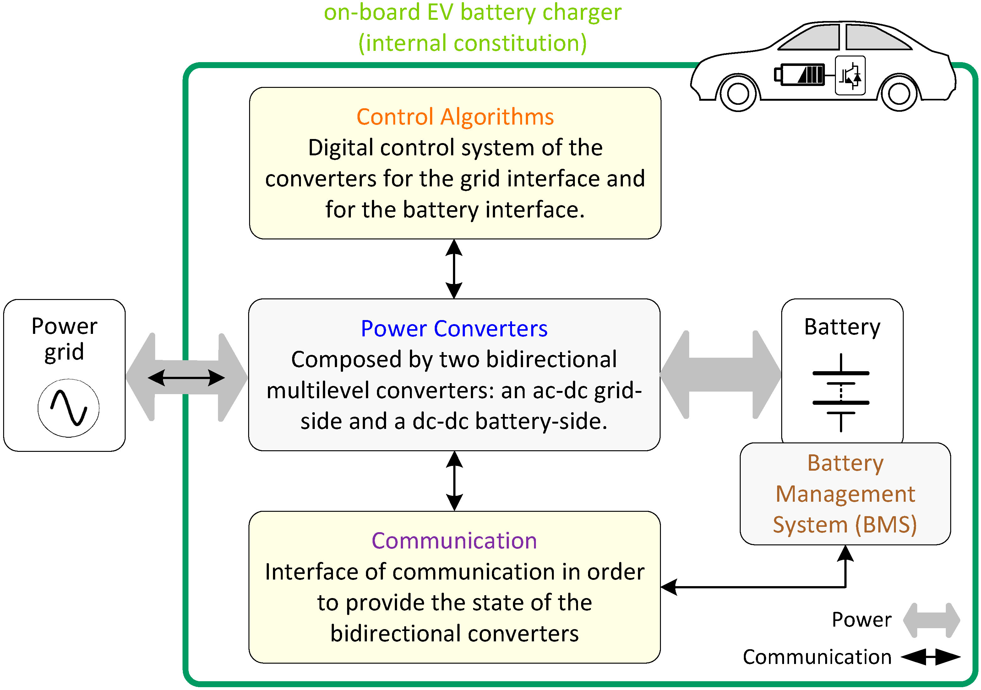
The above-mentioned five-level topologies for the grid-side converter were validated in the scope of diverse applications, but not all were validated neither compared in the scope of an EVBC. The same occurs with the battery-side converter. Moreover, no EVBC was validated employing multilevel topologies in the grid-side and the battery-side converters. In this sense, this paper proposes an on-board EVBC multilevel topology. The internal constitution of a conventional on-board EVBC is presented in Figure 1, where is highlighted the bidirectional power flow, between the batteries and the grid, in order to accomplish with the grid-to-vehicle and vehicle-to-grid operations in smart grids. The key contributions of this paper are: (a) a novel EVBC based on a multilevel topology; (b) an analysis of the proposed EVBC in terms of operation targeting smart grids; and (c) an experimental validation using a dedicated developed on-board EVBC.
The paper is outlined as follows: A description of the hardware topology of the proposed EVBC is presented in Section 2. The discrete-time predictive control algorithms used for the grid-side converter and for the battery-side converter are presented in Section 3. The foremost experimental results considering diverse operating states for smart grids are presented in Section 4. The main conclusions are discussed in Section 5.
2. EV Battery Charger: Topology Description
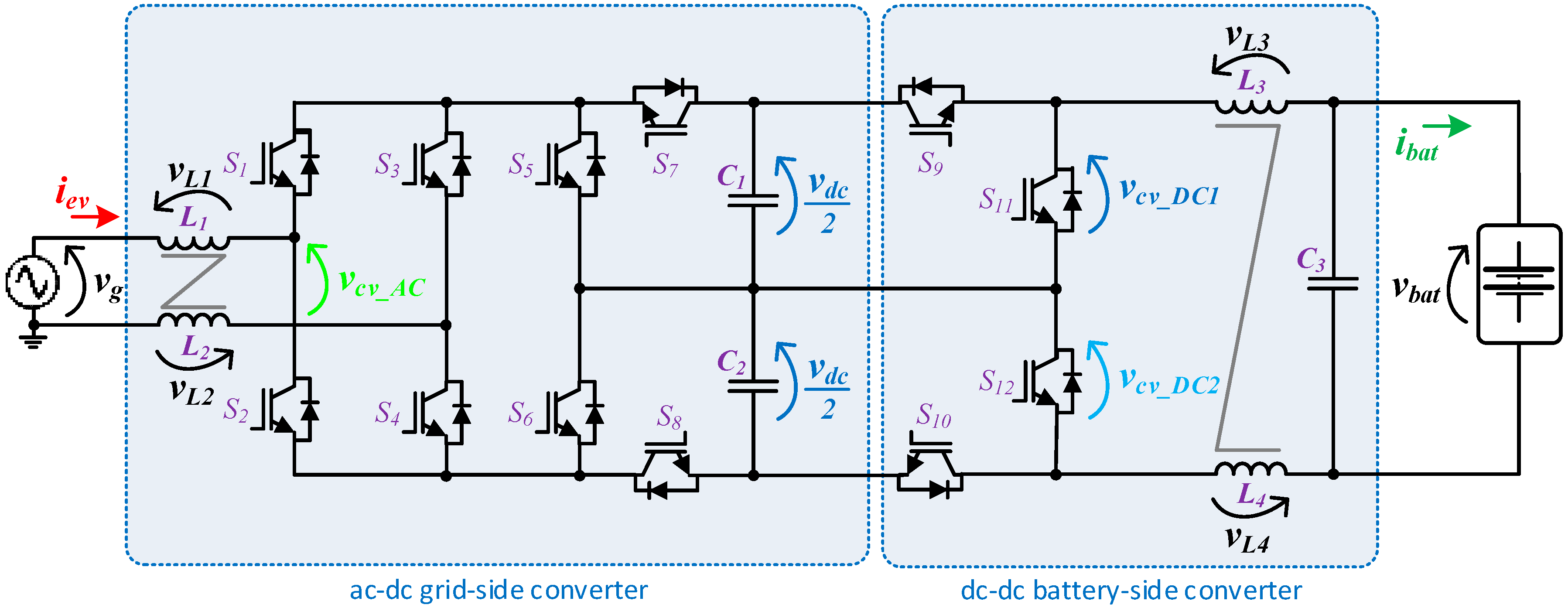
Figure 2 shows the global electrical schematic of the proposed EVBC. This topology consists of a grid-side converter and a battery-side converter, both with a multilevel characteristic supported by a split DC-link formed by two sets of capacitors (C1 and C2). In terms of other components, the EVBC consists of twelve insulated-gate bipolar transistors (IGBTs) (used as controlled switching devices, eight for the grid-side converter and four the battery-side converter), an inductive coupling filter (L1, L2), and a LC passive filter interfacing the batteries (L3, L4 and C3).
The values of the parameters constituting the on-board EVBC, as well as the specifications of the system that was taken into account when choosing components, are given in Table 1.
2.1. Topology Description: Grid-Side Converter
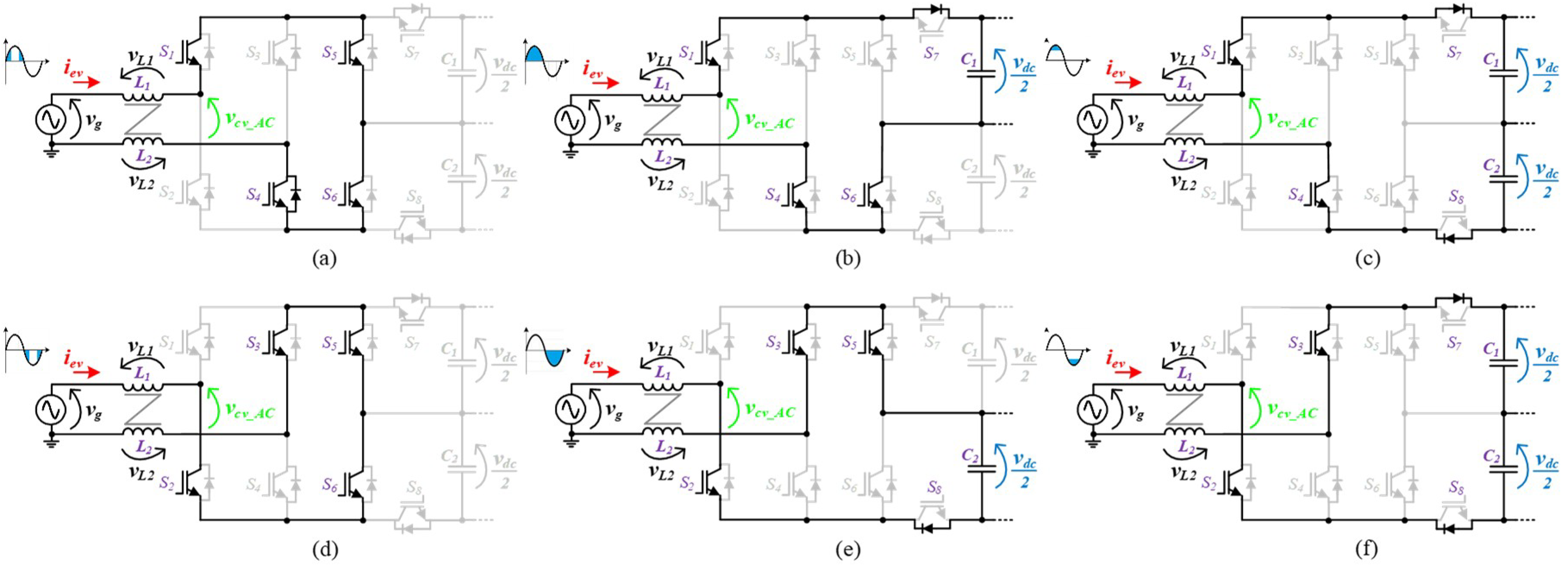
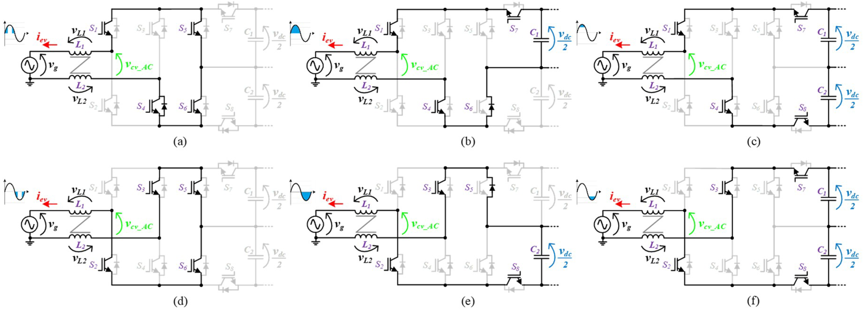
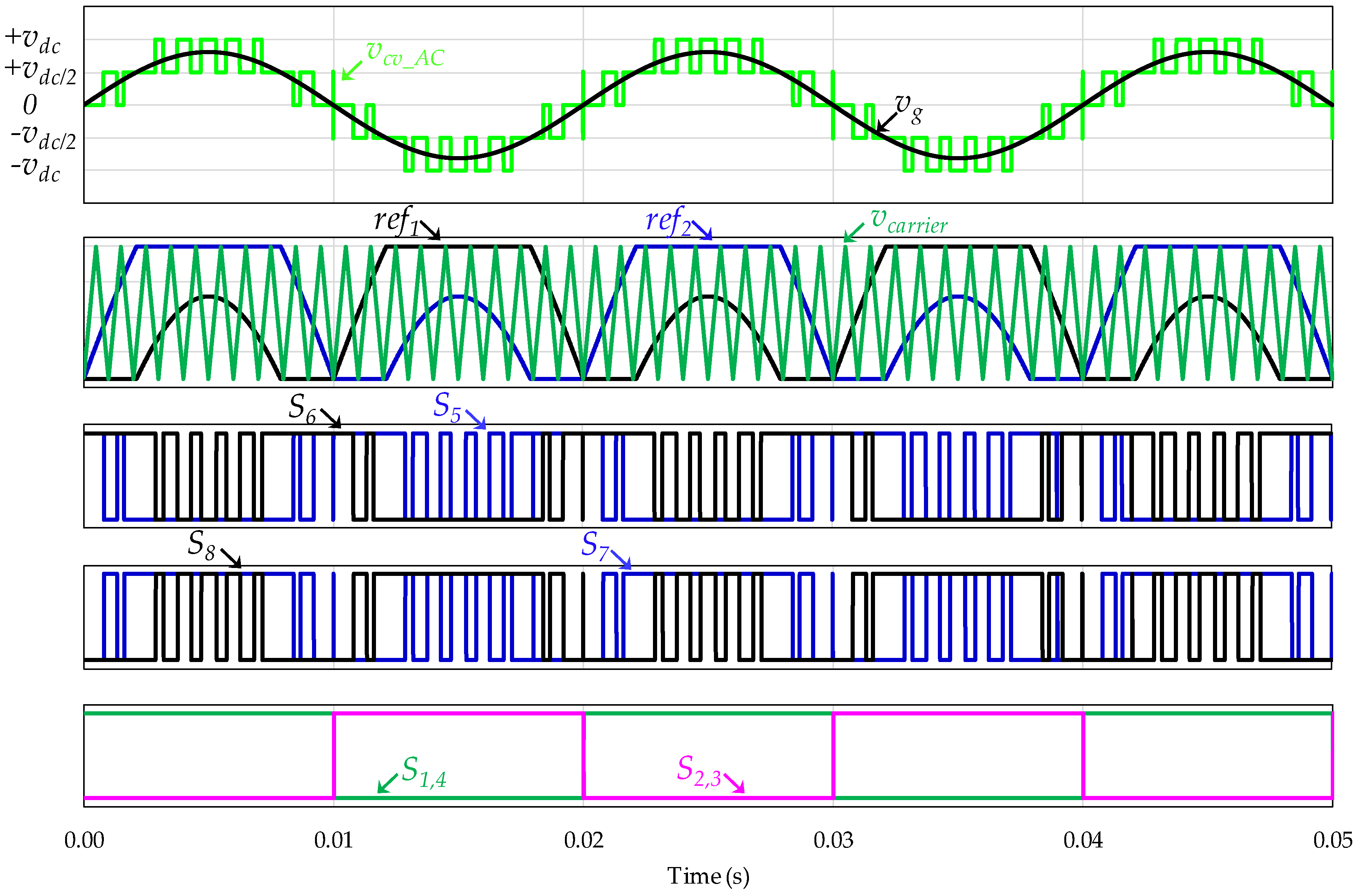
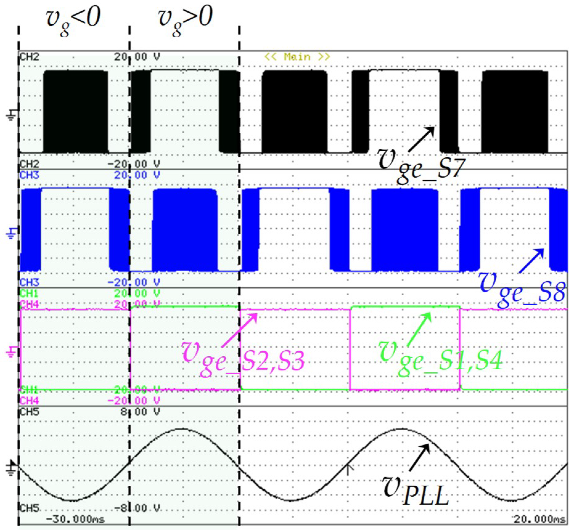
In the development of power electronics systems, electrical grid power quality issues are, more than ever, a major concern. Since the voltage levels produced by grid-side multilevel converters are directly proportional to the quality of the obtained grid current, multilevel converters have emerged as contributors for this concern. The circuit topology of the grid-side multilevel converter proposed for the on-board EVBC is presented in Figure 2. The proposed topology emerged as a derivation of the traditional full-bride rectifier with four devices connected to the split DC-link as the power factor correction (PFC) three-level DC-DC converter. This topology can produce five distinct voltage levels (+vdc, +vdc/2, 0, −vdc/2, −vdc) at the terminals of the converter (vcv_AC). As can be seen, each IGBT is applied to a maximum voltage of +vdc. The configuration of the topology allows to switch necessarily only six of the eight IGBTs, during the full operation as active rectifier or grid-tied inverter, hence, decreasing the switching losses. When the grid side converter operates as active rectifier, Figure 3, during the positive half cycle of the power grid voltage, the IGBTs (S1, S4) are always switched on and the IGBTs (S2, S3) are always switched off. When the IGBT S6 is switched on, the IGBT S5 is switched to state the voltage levels 0 and +vdc/2. On the other hand, when the IGBT S5 is switched off, the IGBT S6 is switched to state the voltage levels +vdc/2 and +vdc. During the negative half cycle of the power grid voltage, the IGBTs (S2, S3) are always switched on and the IGBTs (S1, S4) are always switched off. When the IGBT S5 is switched on, the IGBT S6 is switched to state the voltage levels 0 and −vdc/2. Finally, when the IGBT S6 is switched off, the IGBT S5 is switched to state the voltage levels −vdc/2 and −vdc. When the grid side converter operates as an inverter, Figure 4, during the positive half cycle of the power grid voltage, the IGBTs (S1, S4) are always switched on and the IGBTs (S2, S3) are always switched off. When the IGBT S8 is switched off, the IGBT S7 is switched to state the voltage levels 0 and +vdc/2. On the other hand, when the IGBT S7 is switched on, the IGBT S8 is switched to state the voltage levels +vdc/2 and +vdc. During the negative half cycle of the power grid voltage, the IGBTs (S2, S3) are always switched on and the IGBTs (S1, S4) are always switched off. When the IGBT S7 is switched off, the IGBT S8 is switched to state the voltage levels 0 and −vdc/2. Finally, when the IGBT S8 is switched on, the IGBT S7 is switched to state the voltage levels −vdc/2 and −vdc.
A predictive current control technique, with a fixed switching frequency of 20 kHz, was applied to obtain a sinusoidal EVBC current and in phase with the grid voltage (or phase opposition in vehicle-to-grid mode). Since this current control is identified as a linear current control, the modulation technique is applied individually. In this sense, Figure 5 shows the pulse-width modulation (PWM) modulation technique arrangement used for the grid-side converter. The proposed PWM modulation technique requires only one carrier signal and two reference signals to control eight IGBTs. This figure shows the adapted voltage reference (ref1, ref2), the triangular carrier signal (vcarrier), the PWM signals of the IGBTs, the voltage levels produced by the converter (vcv_AC) and the power grid voltage (vg). The pulses signal of the IGBTs (S1, S2, S3, S4) are exclusively dependent of the instantaneous value of the power grid voltage. During the operation as grid-tied inverter, the IGBTs (S7, S8) have an opposite a command signal as the IGBTs (S5, S6), respectively. In the modulation strategy, the voltages references (ref1, ref2) are adapted, based on a digital codification, from the modulating signal sM established by the Equation (1), where vcv_AC are the voltage levels produced by the converter and ma the amplitude modulation index. The voltage levels produced by the converter are obtained in the control algorithm, explained in Section 3.1.
2.2. Topology Description: Battery-Side Converter
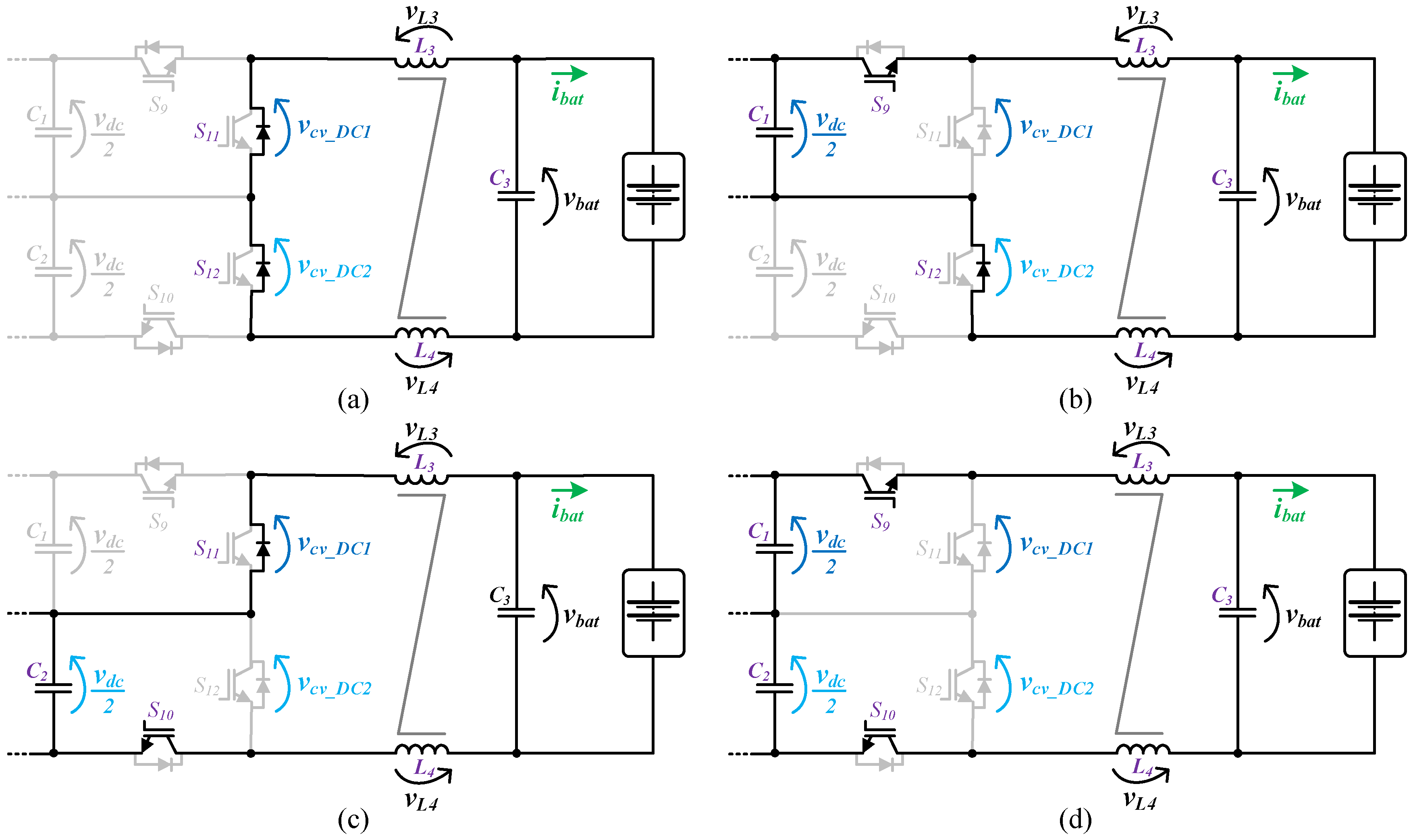
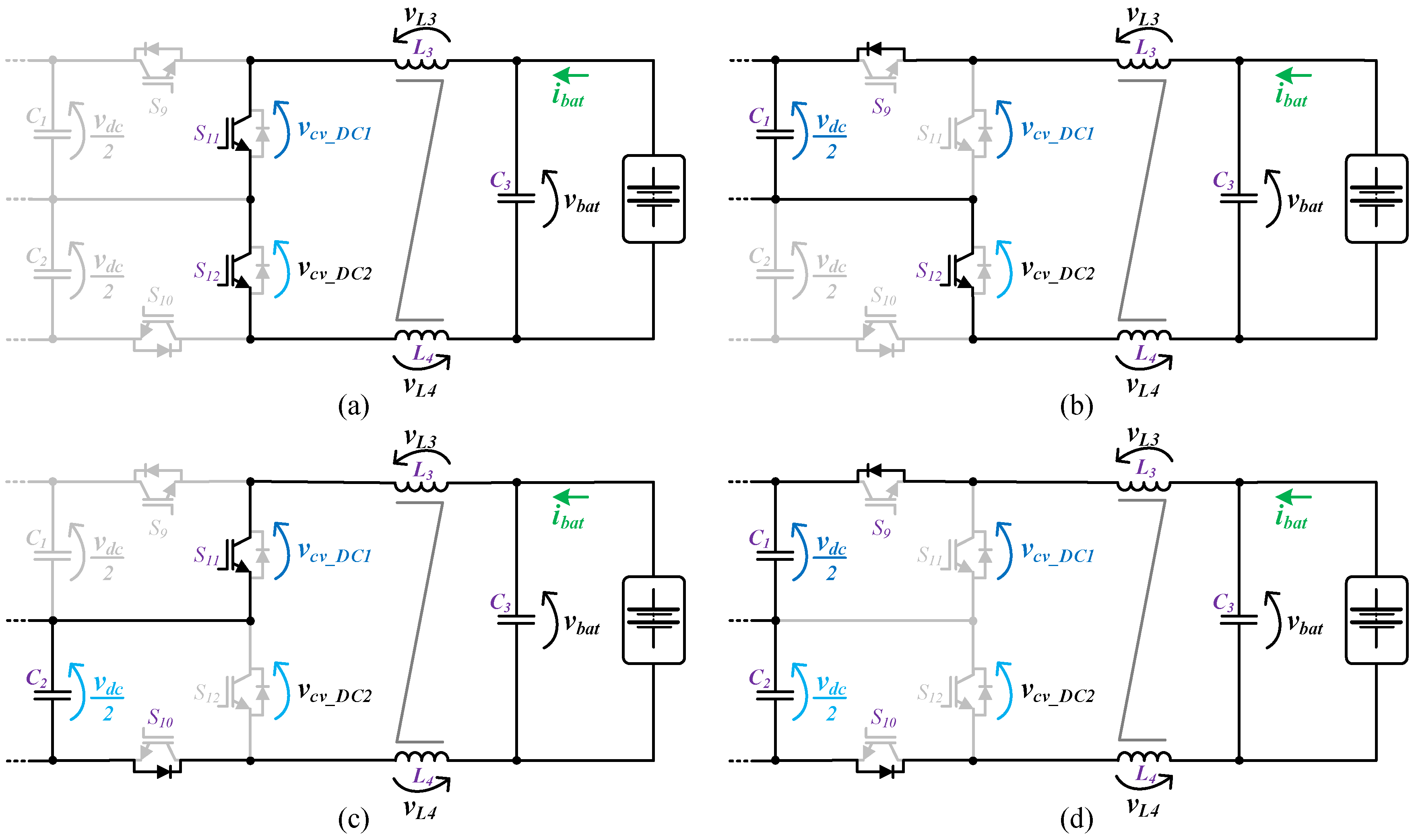
The circuit topology of the battery-side converter implemented in the on-board EVBC is presented in Figure 2. The topology consists in four IGBTs connected to the split DC-link and a passive LC filter interfacing the batteries. Furthermore, this topology can produce three distinct voltage levels (+vdc, +vdc/2, 0) at the terminals of the converter (vcv_DC). When the converter operates as a buck-type converter, the energy power flows of the DC-link to the batteries during the charging process. In this mode, the IGBTs (S9, S10) and the anti-parallel diodes of the IGBTs (S11, S12) are used. When only one of the IGBTs (S9, S10) is switched on, the inductors (L3, L4) and the batteries stores energy from the split DC-link (C1 or C2). When both IGBTs (S9, S10) are switched on, the inductors (L3, L4) and the batteries store energy from the DC-link (C1, C2). When both IGBTs (S9, S10) are switched off, the stored energy in the inductors (L3, L4) is released to the batteries. On the other hand, when the converter operates as boost-type converter, the energy power flows of the batteries to the DC-link, during the discharging process. During this mode, the IGBTs (S11, S12) and the anti-parallel diodes of the IGBTs (S9, S10) are used. When both IGBTs (S11, S12) are switched on, the inductors (L3, L4) stores energy from the batteries. When one of the IGBTs (S11, S12) is switched on, the split DC-link (C1 or C2) stores energy from the batteries and the inductors (L3, L4). Finally, when both IGBTs (S11, S12) are switched off, the DC-link (C1, C2) stores energy from the batteries and the inductors (L3, L4). Figure 6 and Figure 7 show the operation stages for the battery-side converter during the operation as buck-type and boost-type, respectively.
Similar to the algorithm applied in the grid-side converter, in the battery-side converter was also applied a predictive current control technique and a modulation technique with a fixed switching frequency of 20 kHz, to control the current and voltage in the batteries during the charging or discharging processes. In the modulation technique, two 180° phase-shifted carriers were used, in order to reduce the ripple of the EV battery current and, hence, the frequency EV battery current is held twice of the switching frequency.
3. EV Battery Charger: Control Algorithms
This section presents the specifications and the methodology used for the control algorithms implementation, both for the grid-side and the battery-side converters. The control algorithm was designed for a digital platform, based on a Texas Instruments digital signal processor (DSP) F28335 (Texas Instruments, Inc., Dallas, TX, USA) and considering a sampling frequency of 40 kHz, obtained with a timer interruption.
3.1. Control Algorithm: Grid-Side Converter
Based on the voltages shown in Figure 2, Equation (2) can be established, where vg represents the instantaneous value of the grid voltage, vL1 and vL2 the instantaneous value of the inductance voltage, and vcv_AC is the instantaneous value (i.e., the voltage produced during each sampling period of the DSP) of the voltage produced by the converter:
It should be noted that, as represented in Figure 2, it was used a mutual coupling inductance. Therefore, replacing the inductance voltage by its intrinsic equation, and rewriting the equation as a function of the voltage produced by the converter, it is obtained:
Applying the progressive Euler method, illustrated in Equation (4), the derivative component of the current can be approximated by considering a very low Δt in order to obtain a good prediction of the system behavior:
Applying the Equation (4) in the Equation (3), and assuming a sampling frequency of fs = 1/Ts, results in the digital control Equation (5), where the term k represents the current sample and [k + 1] represents the next sample:
Since the law of predictive control consists of a closed-loop control and, if the reference current at time [k + 1] is to be equal to the current produced by the converter at time [k], the equation that translates the current control implemented can be defined by:
Since, the EVBC is proposed to operate with a sinusoidal current and unitary power factor in the grid-side converter, the instantaneous value of the power grid voltage is directly proportional to the EVBC current. However, aiming to prevent the inclusion of the harmonic distortion of the grid voltage into the current, it is used a phase-locked loop (PLL). Thus, instead of the grid voltage, it is used the output signal from the PLL, resulting in:
where vpll is in phase with the power grid voltage and Gev represents the equivalent conductance of the EVBC from the grid-side point of view, which can be defined according to the mean value of active power (Pev) and the rms value of the power grid voltage (Vg):
Applying the Equation (8) in the Equation (7), the reference of the EVBC current is obtained according to:
The active power of the EVBC can be divided in two parts, namely the power to regulate the DC-link voltage and the power to regulate the batteries. Furthermore, because of the split DC-link, two proportional-integral (PI) are used to regulate the DC-link voltage independently in both capacitors (pdc1, pdc2). Therefore, during the G2V operation mode, the reference of the EVBC current can be defined as:
On the other hand, during the V2G operation mode, the reference of the EVBC current is established according to Equation (11), where ibat* represent the reference of current to discharge the batteries.
3.2. Control Algorithm: Battery-Side Converter
During the process of charging the batteries, the battery-side converter operates as buck converter, controlling the charging current or the charging voltage for the batteries. In this way, based on the representations of the currents and voltages between the DC-link and the batteries (cf. Figure 2), it is possible to establish the Equation (12), where vcv_DC represents the voltage produced by the converter (i.e., the sum between vcv_DC1 and vcv_DC2), vL3 and vL4 represent the voltages in the inductances (L3 and L4), respectively, and vbat represents the voltage in the batteries:
Since the current in the inductance L3 is the same as that in the inductance L4, the Equation (12) can be rewritten, replacing the voltage in the inductance by its intrinsic equation:
Applying the progressive Euler method, the Equation (13) can be established in discrete time as:
Since it is desired that the reference current at time [k + 1] should be equal to the current produced by the converter at time [k], it is obtained:
When the same converter operates as buck converter, but controlling the charging voltage of the batteries, the reference voltage is established as:
The aforementioned equations were defined for the battery-side converter operating as buck converter, i.e., charging the batteries from the grid (G2V mode). On the other hand, a set of equations should also be defined for the battery-side converter operating as boost converter, i.e., discharging the batteries to the grid (V2G mode). Based on the representations of the currents and voltages in Figure 2, when the converter intends to discharge the batteries with a constant current, the following relation can be established:
Applying the same aforementioned modeling reasoning, the discrete implementation of Equation (17) results in:
From Equation (18), it is important to note that it is necessary to identify the positive direction of the current in the batteries (Figure 2), which is why the negative signal −iL3,L4*[k + 1] is applied to the digital implementation of this equation. The obtained signal (vcv_DC[k]) is compared with two carriers in order to obtain the duty-cycle of the gate signals for S9 and S10, which is the same, but two carriers, delayed by 180 degrees, are employed. Applying this strategy, the frequency of the resultant ripple is the double of the switching frequency. The duty-cycle is determined according to the current control algorithm, e.g., in the previous equations is defined the a voltage that is compared with the carriers in order to obtain a current in the EV battery i(L3,L4)[k] equal to the reference current i(L3,L4)*[k]. Applying this strategy, the current ripple in the EV battery can be reduced when compared with a traditional buck or boost converter. In circumstances where the battery-side converter is responsible for controlling the voltage on the DC-link, the Equation (19) is implemented, where represents the duty-cycle that the converter must produce, vdc* represents the reference voltage for the DC-link, and vbat represents the battery voltage:
4. EV Battery Charger: Experimental Validation
This section introduces the experimental validation, where is presented the hardware description, as well as the most relevant experimental results.
4.1. Description of the Developed Prototype
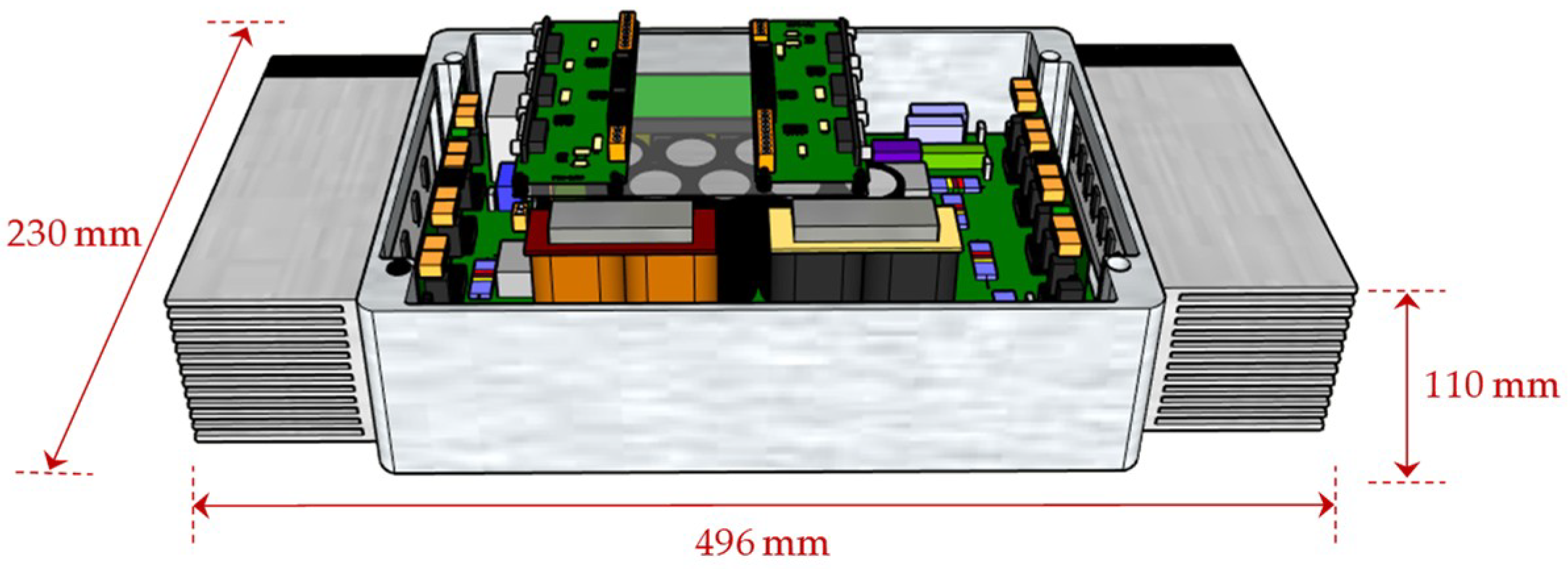
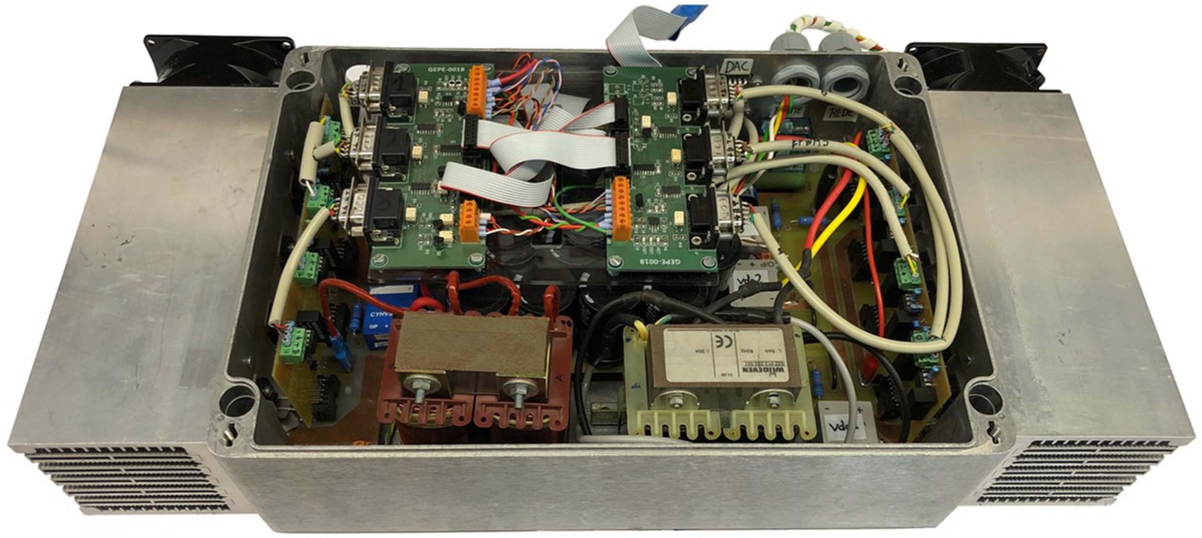
After the computer validation, a laboratory prototype of the on-board EVBC was implemented, which is mainly divided in two parts: the digital control platform and the power hardware. The digital control platform includes the DSP board (F28335), the current and voltage sensors (models LTSR15 NP and CYHVS025A from LEM (Geneva, Switzerland) and from ChenYang (Finsing, Germany), respectively), as well as the printed circuit boards of the signal conditioning, error detection, command, and gate drivers (developed with HCPL 3120 optocouplers from Avago). On the other hand, the power hardware includes both converters, constituted by discrete IGBTs (FGA25N120ANTD from Fairchild (Sunnyvale, CA, USA)) and by the DC-link capacitors (EETUQ2W561DA from Panasonic (Kadoma, Japan)). Since the main aim of the implementation was the development of a laboratory prototype as close as possible of the reality, namely in compactness and robustness, a three-dimensional modeling was carried out to determine the best method and solution of the component layout for its implementation. Figure 8 shows the internal and external view of the three-dimensional modeling of the EVBC. With this modeling, it was possible to implement the final laboratorial prototype, which is presented in Figure 9. However, it should be noted that the laboratory prototype was developed just aiming to validate the structure of the topology and to perform a laboratorial experimental validation. In fact, after the proof-of-concept in terms of topology and operation modes, some improvements are required focusing in the optimization of the switching devices (e.g., employing SiC devices) and in the optimization of the passive filters (e.g., employing a inductor-capacitor-inductor, LCL, filter) toward a pre-industrialized prototype.
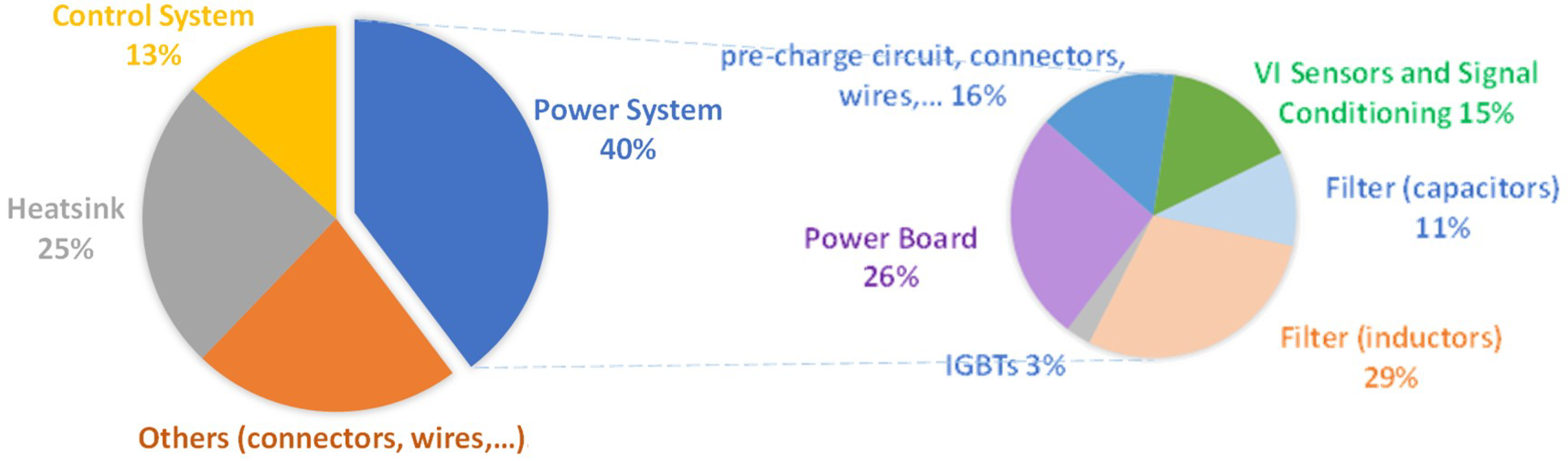
The converters of the developed prototype were sized to meet the key requirements of the proposed on-board EVBC in terms of power quality, and the specifications given in Table 1. In this sense, the choice of components was mainly based on their operational characteristics, such as the maximum operating frequency and the rated current and voltage. In addition to the electrical aspects of the concerned application, mechanical and thermal aspects, such as dimensions, encapsulation and thermal dissipation of components, have also been taken into account, since the entire system is integrated in a metal box (Bernstein CA 380 (Porta Westfalica, Germany)), with dimensions of 330 × 230 × 110 mm. As it can be seen, two heatsinks were used, one for each converter, which were fixed on each side of the metal box. In order to prevent electrical noise, it was decided to place the gate driver boards as close as possible to the power semiconductors, each one responsible for a power electronics converter. In the control system, electrical noise was also taken into account in order to optimize the signal-to-noise ratio, i.e., to minimize undesired signals superimposed on a measured signal. Based on the developed three-dimensional modeling and the implemented prototype, an estimation of the internal volume distribution associated to the different main parts of the on-board EVBC was established, which is presented in Figure 10.
4.2. Experimental Results
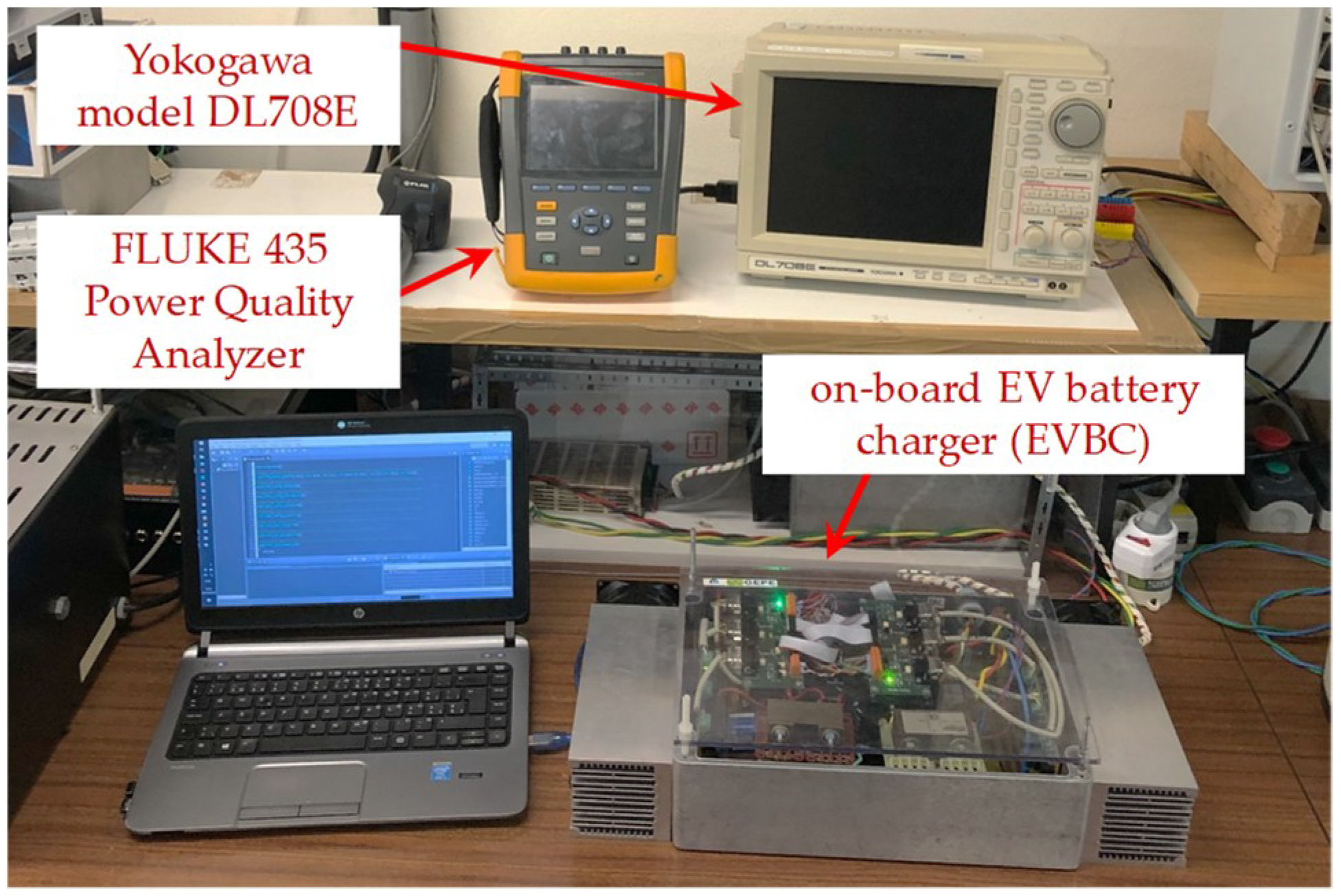
In the on-board EVBC laboratorial prototype described above, the G2V operation mode was initially validated, followed by the V2G. Besides the validation of both operations mode, the experimental results also demonstrate the validation of the PLL algorithm, modulation and current control strategy and DC-link voltage control. Figure 11 presents the general view of the laboratorial setup that was used during the experimental results, which were registered with a digital oscilloscope Yokogawa model DL708E (Yokogawa Electric, Tokyo, Japan), with a Fluke 435 power quality analyzer (Fluke Corporation, Everett, WA, USA), and with a FLIR i7 infrared thermal imaging camera (FLIR Systems, Wilsonville, OR, USA).
4.2.1. Experimental Results: Grid-To-Vehicle (G2V) Operation
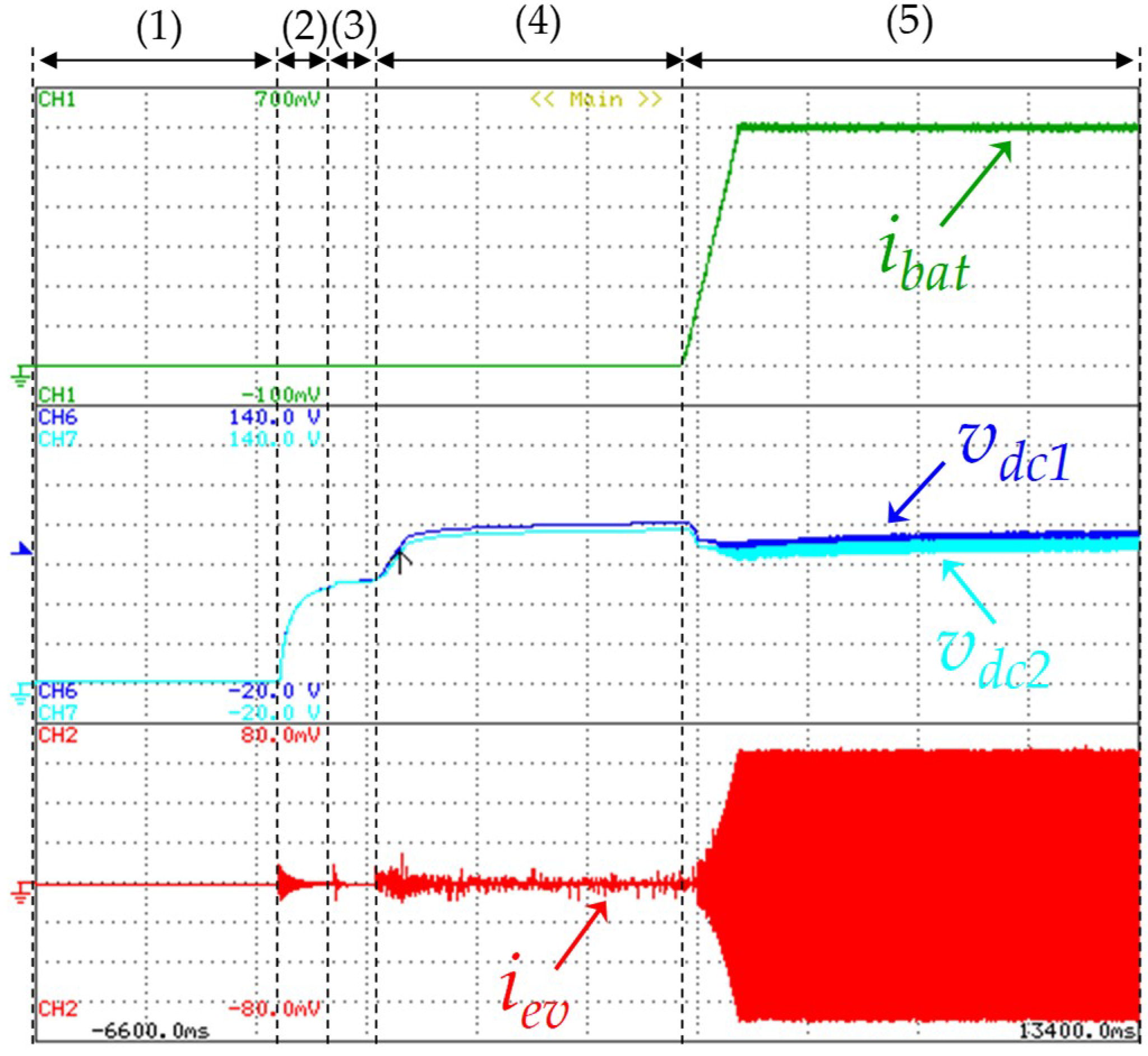
Figure 12 shows the experimental results during the initial stage of the EV charging process. First, during the time interval (1) the EVBC is not connected to the power grid. At time instant (2), the EVBC is connected to the power grid. In this stage, the DC-link start the pre-charge process through the anti-parallel diodes of the IGBTs (S1, S2, S3, S4), operating the grid-side converter as a traditional full-bridge rectifier. The pre-charge circuit contains a resistor to limit the typical peak currents of the capacitors. After the DC-link pre-charge process, at time instant (3), this resistor is bypassed so that the DC-link voltage remains close to the peak value of the grid voltage. At time instant (4), the split DC-link voltage, in each capacitor, is regulated to the operation voltage and only after stabilizing the DC-link voltage, at time instant (5), the current battery increases progressively (i.e., during the constant current algorithm), which is controlled by the battery-side converter operating as buck converter.
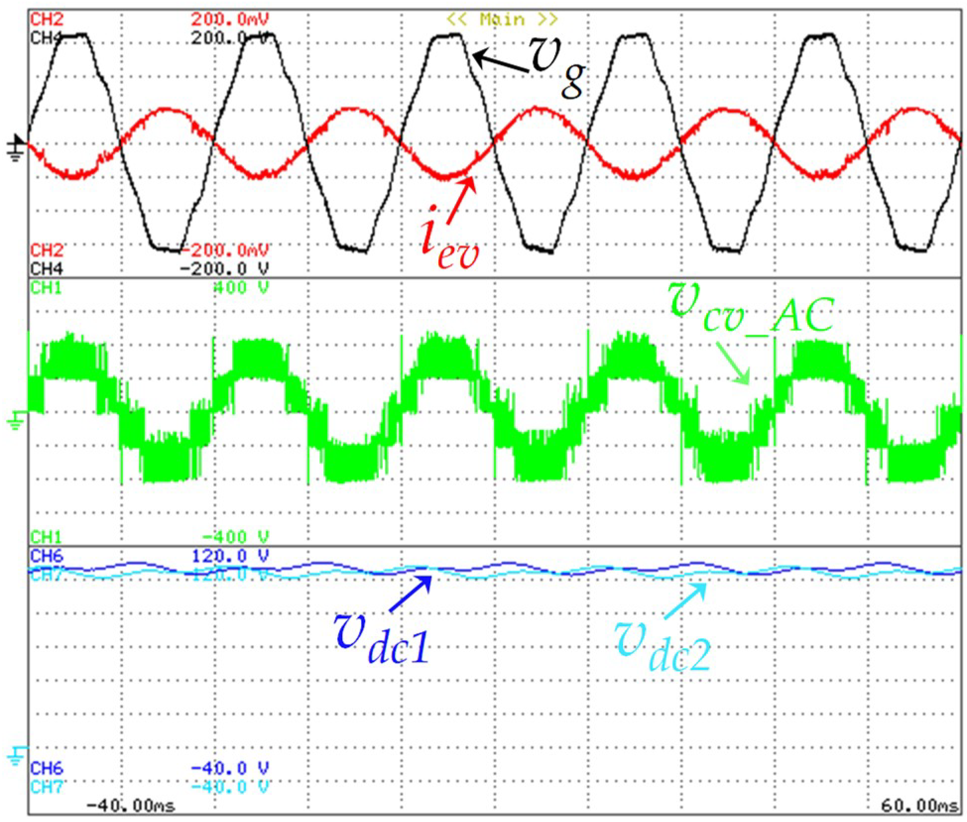
As clearly shown in Figure 13, the grid voltage is distorted due to the nonlinear electrical appliances linked in the electrical installation. However, during a steady-state operation, with the adopted current control strategy, the EVBC current is kept with a sinusoidal waveform and in phase with the grid voltage (i.e., operating with a unitary power factor, as shown in the zoom detail presented in this figure). Furthermore, the DC-link voltage in both capacitors presents an acceptable ripple for this type of application (i.e., about 10%). The average voltage value in each DC-link capacitor is controlled according to each reference, assuming a value which is greater than the maximum amplitude of the power grid voltage, and the ripple in the voltages of the capacitors has a frequency that is double the frequency of the power grid. In this operation mode the measured efficiency was 92%.
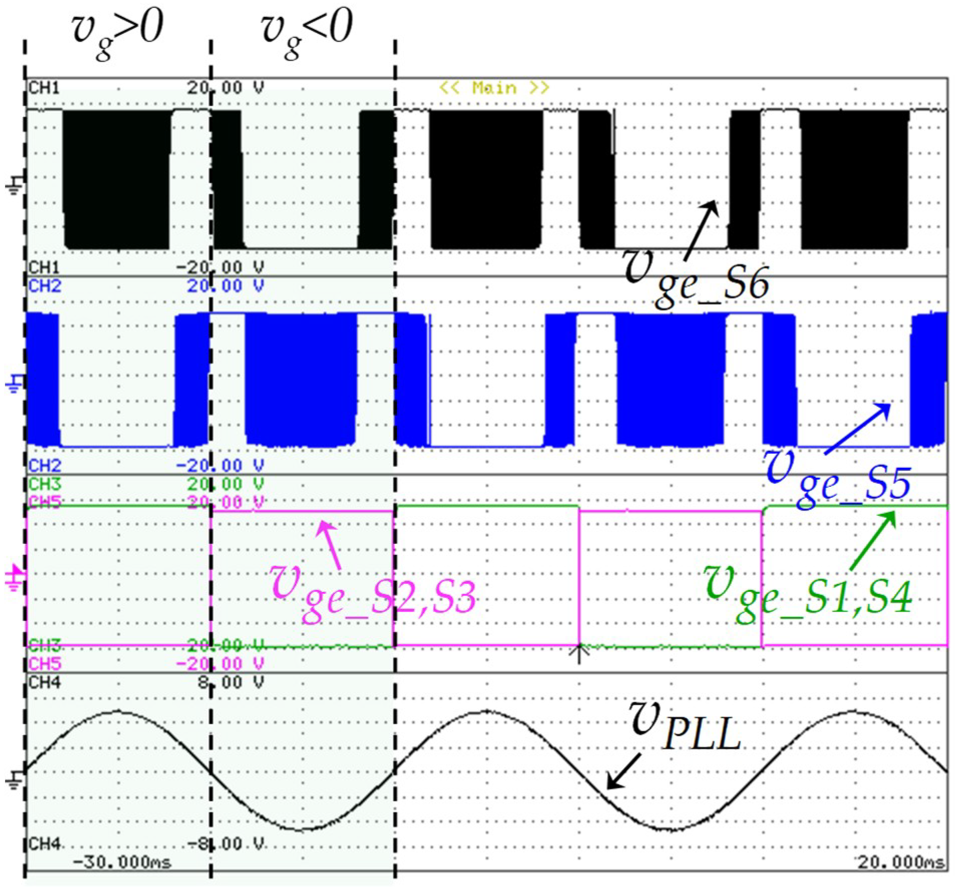
The experimental results shown in Figure 14 were attained to verify the switching states of the grid-side converter according the Figure 3. The IGBTs S1, S2, S3, and S4, as well as the IGBTs S5 and S6, have a fixed switching frequency of 50 Hz and 20 kHz, respectively. This figure also shows the digital signal obtained from the PLL algorithm, which is sinusoidal and in phase with grid voltage. This signal was visualized in the oscilloscope using an external digital-to-analog converter (DAC), model TLV5610 from Texas Instruments.
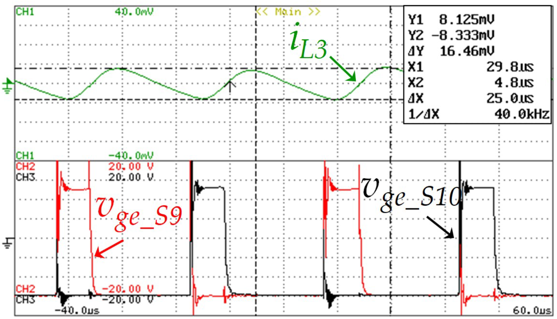
The PWM technique developed for the battery-side converter consists in two carriers with a 180° phase-shifting. With this phase-shifting strategy, one of the gate signals is applied to IGBT S9 while the other is applied to the IGBT S10, to reduce the ripple of the EV battery current. Thus, as it can be seen in Figure 15, the frequency of the current ripple in the inductor L3 (iL3) is 40 kHz, which is twice of the switching frequency. This experimental result shows the relation of the current in the inductor and the gate-emitter voltage, vge_S9 and vge_S10, of the IGTBs S9 and S10. During this result, the registered value of the ripple current in the inductor was 0.16 A.
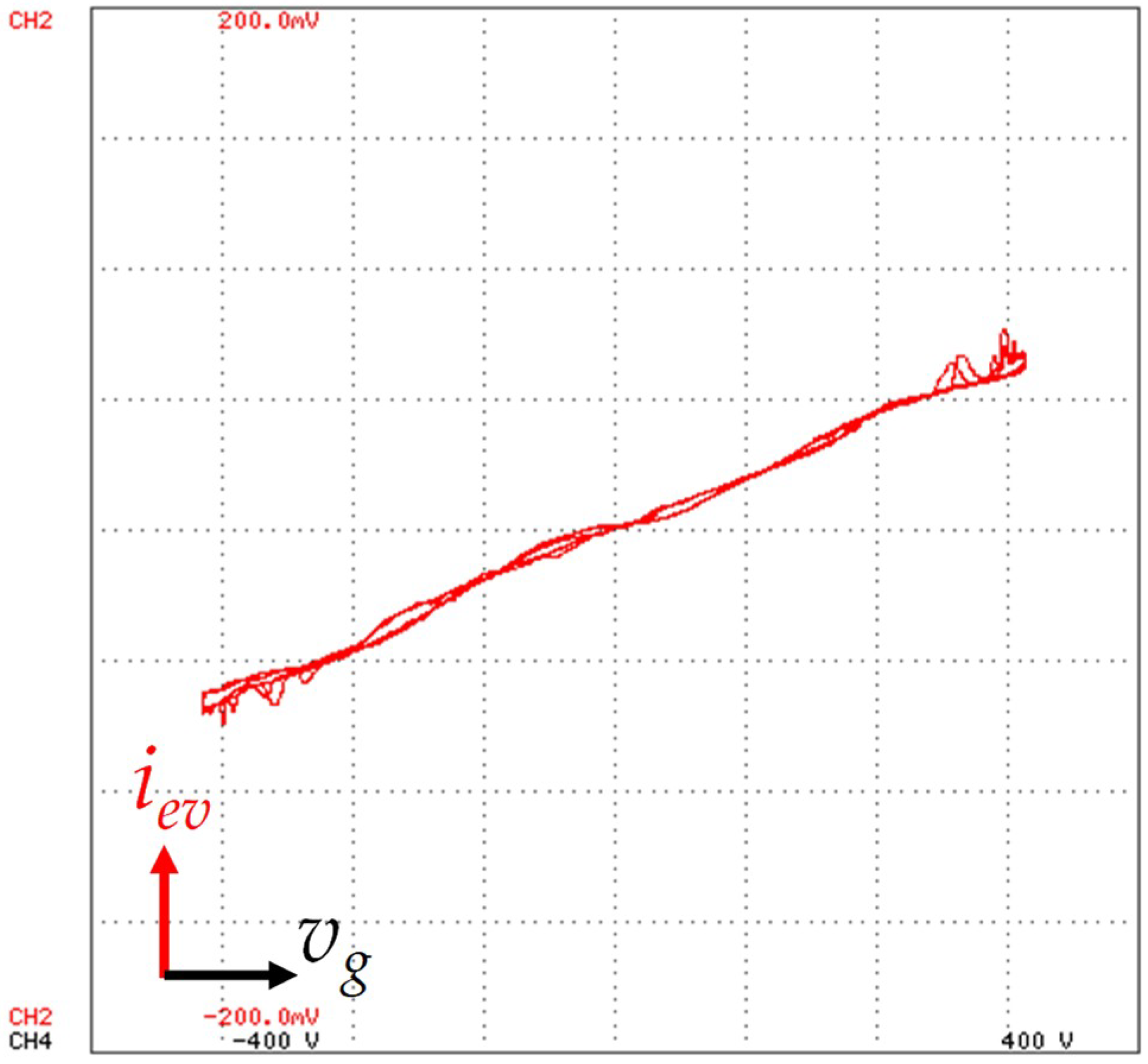
For further details on the relationship between the grid voltage and the EVBC grid-side current, it was used the x-y mode of the oscilloscope, as shown in Figure 16. Channel 4 is used in the x-axis and the channel 2 is used in the y-axis, representing the grid voltage and EVBC grid-side current, respectively. Thus, for the grid-side, this result shows the EVBC current in function of the grid voltage. It is relevant to highlight that this variation is not linear due to the harmonic distortion present in the grid voltage.
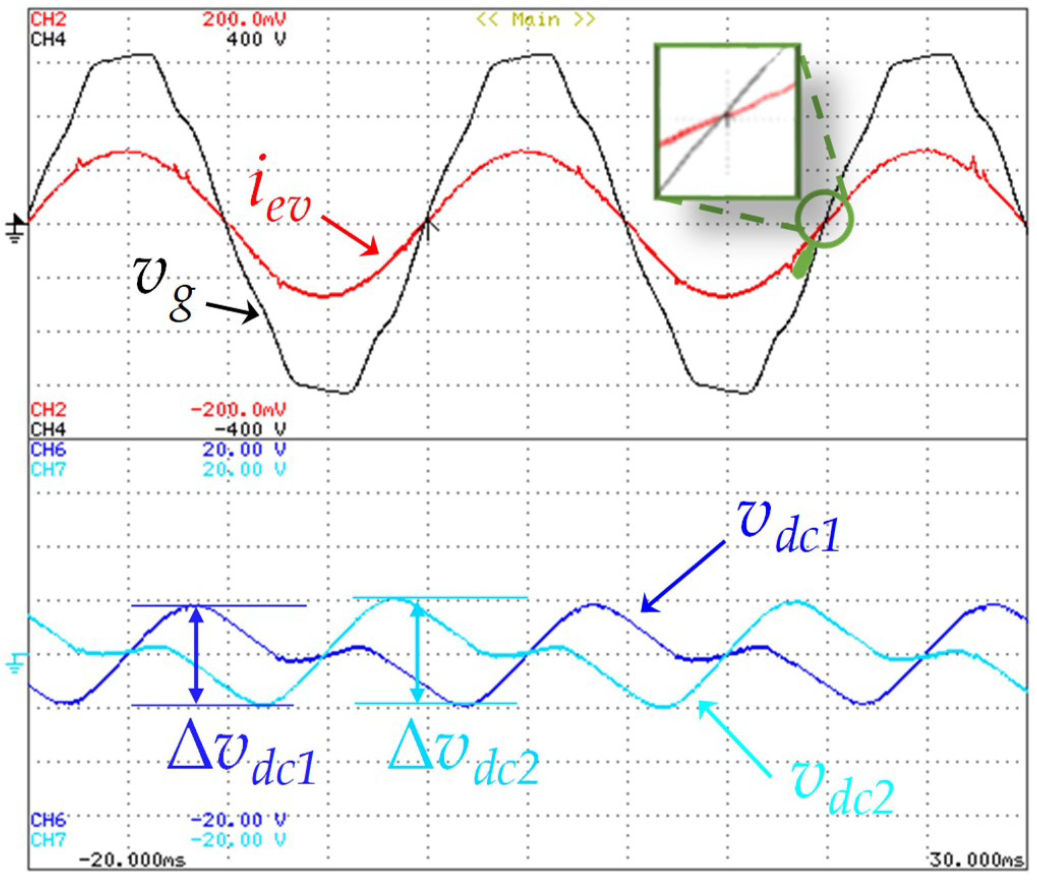
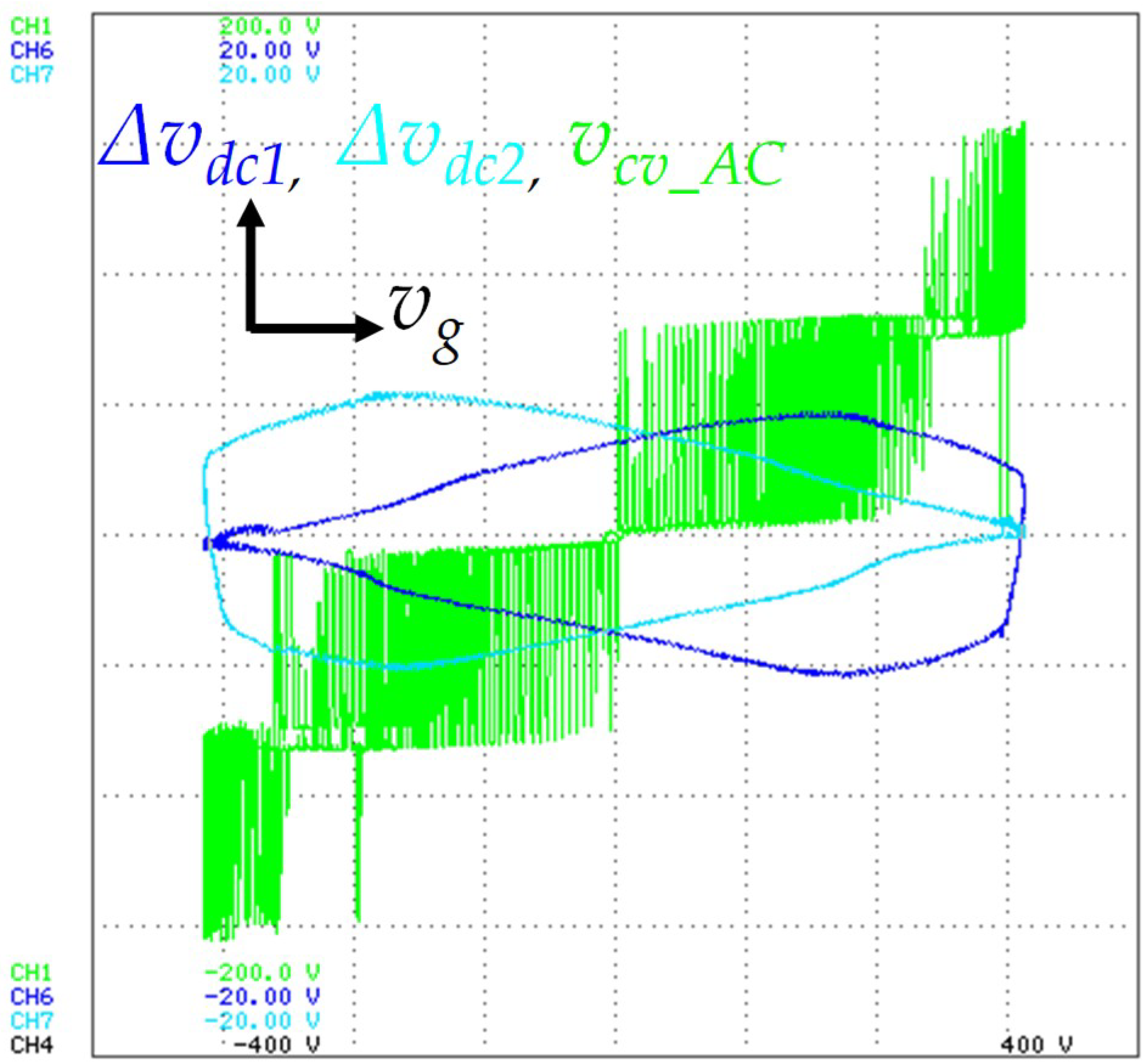
The experimental result shown in Figure 17 was obtained in x-y mode in order to identify the DC-link voltage regulation and to clearly identify the five distinct voltage levels (+vdc, +vdc/2, 0, −vdc/2, −vdc) produced by the grid-side converter. Thus, the DC-link voltage ripple (Δvdc1, Δvdc2) and the voltage levels (vcv_AC), used in the y-axis, are a function of the grid voltage (vg), used in the x-axis. In order to keep the DC-link regulated and balanced, during the positive half-cycle of the grid voltage, the voltage of the capacitor C1 is regulated, and during the negative half-cycle of the grid voltage, the voltage of the capacitor C2 is regulated.
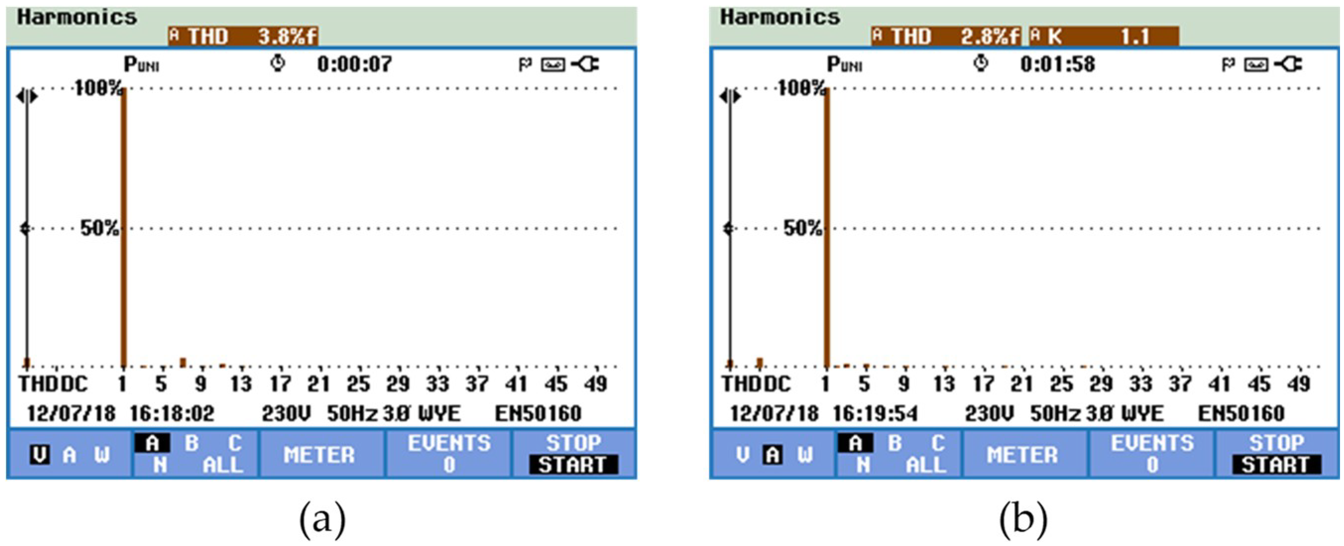
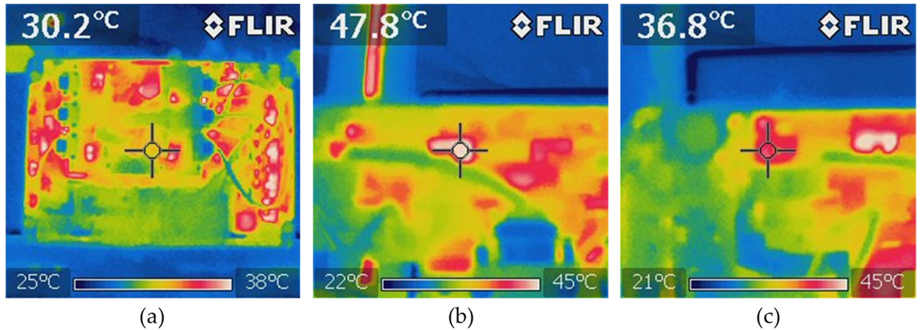
Using the Fluke power quality analyzer, in Figure 18a,b shows the harmonic spectrum of the power grid voltage and the EVBC current, measured total harmonic distortion (THD%) of 3.5% and 2.8%, respectively. In power electronics systems, the thermal characteristic is a factor that directly affects the performance of it. So, to analyse the thermal conditions of the EVBC, the experimental results of temperature measurements during the G2V operation mode are presented in Figure 19. Figure 19a shows the overall thermal distribution of the implemented EVBC, Figure 19b shows the measured temperature of IGBT S9 (switched at a fixed frequency of 20 kHz), where was registered a temperature value of 47.8 °C, and Figure 19c shows the measured temperature of the IGBT S11 (only the antiparallel diode is used in this context), where was registered a temperature value of 36.8 °C.
4.2.2. Experimental Results: Vehicle-To-Grid (V2G) Operation
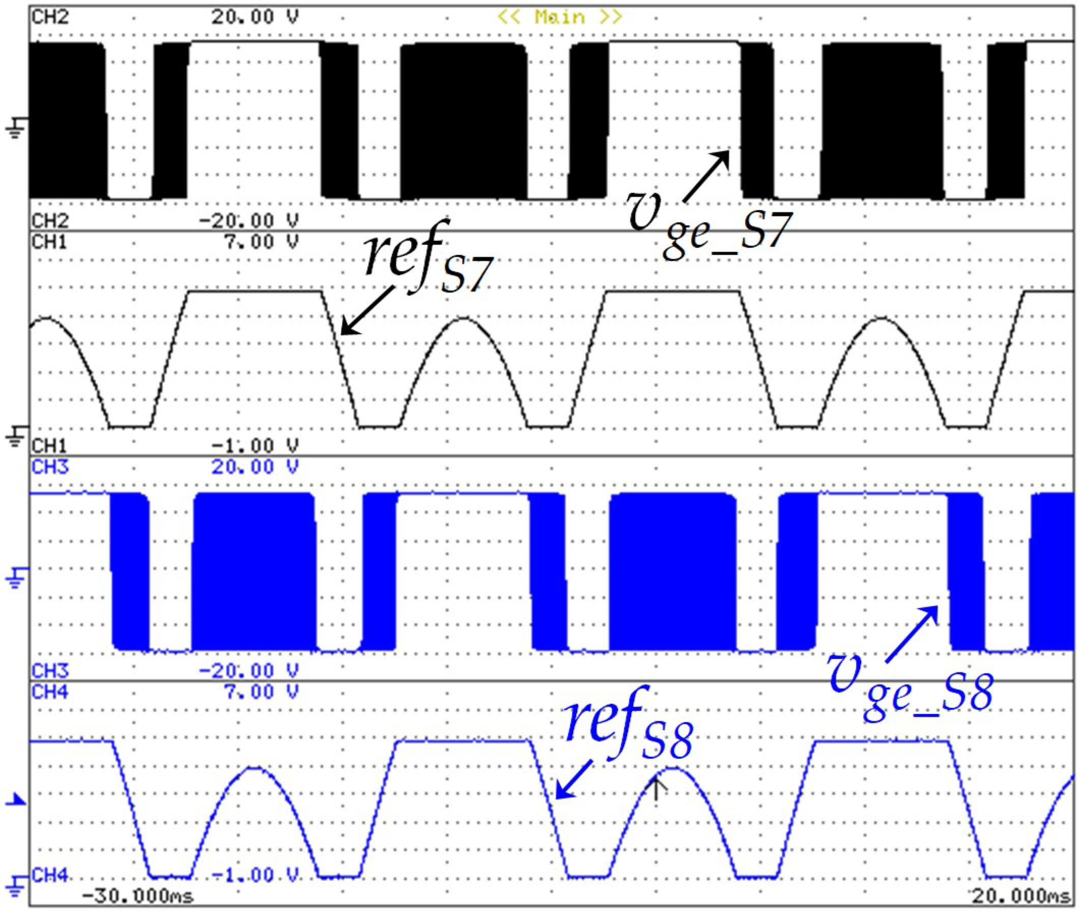
The developed EVBC was also validated during the V2G operation mode. Furthermore, once the IGBTs S7 and S8 of the grid-side converter has a fixed switching frequency of 20 kHz, to validate the modulation technique applied in these IGBTs, Figure 20 presents the reference signal adapted and the gate-emitter voltage of the respective IGBT. This voltage is a resulting signal of the comparison between the carrier signal and the reference signal. In this result, the reference signal was acquired using an external DAC.
Similar to the G2V operation mode, Figure 21 shows the switching states of the grid-side converter according to Figure 3 during the V2G operation mode. In this result, the IGBTs S1, S2, S3, and S4, as well as the IGBTs S7 and S8, have a fixed switching frequency of 50 Hz and 20 kHz, respectively. In this operation mode, the IGBTs (S5, S6) are always switched off, reason why they are not represented in this figure.
Figure 22 shows the V2G operation mode during a steady operation of the EVBC grid-side current (iev), the grid voltage (vg), the voltage levels assumed by the grid-side converter (vcv_AC), and the DC-link voltage of both capacitors (vdc1, vdc2). The EVBC grid-side current is sinusoidal, but in phase opposition with the grid voltage, meaning that the power follows from the batteries to the grid. Furthermore, the five distinct voltage levels (+vdc, +vdc/2, 0, −vdc/2, −vdc) produced by the grid-side converter can be seen in this figure.
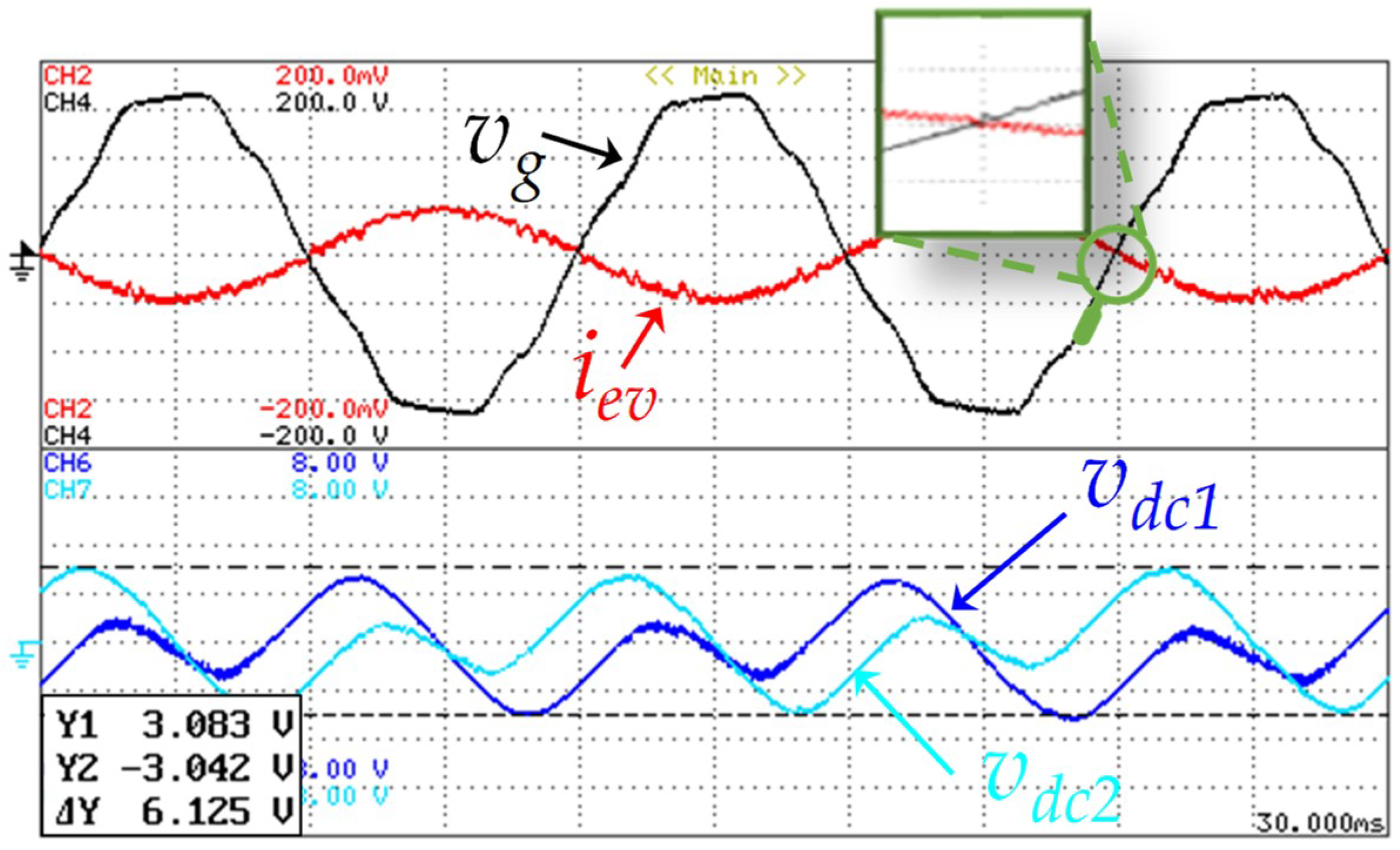
For further details, Figure 23 presents an experimental result, during a time interval of 50 ms, of the EVBC grid-side current (iev), the grid voltage (vg), and the DC-link voltage ripple in both capacitors (Δvdc1, Δvdc2). With the detail of the current zero-crossing, it is possible to state that during these results the EVBC operates with unitary power factor. As aforementioned, during the positive half-cycle of the power grid voltage, the voltage of the capacitor C1 is regulated and during the negative half-cycle of the power gird voltage, the voltage of the capacitor C2 is regulated, which are controlled by the grid-side converter. Moreover, as it can be seen in this figure, the DC-link voltage has a voltage ripple of 3%.
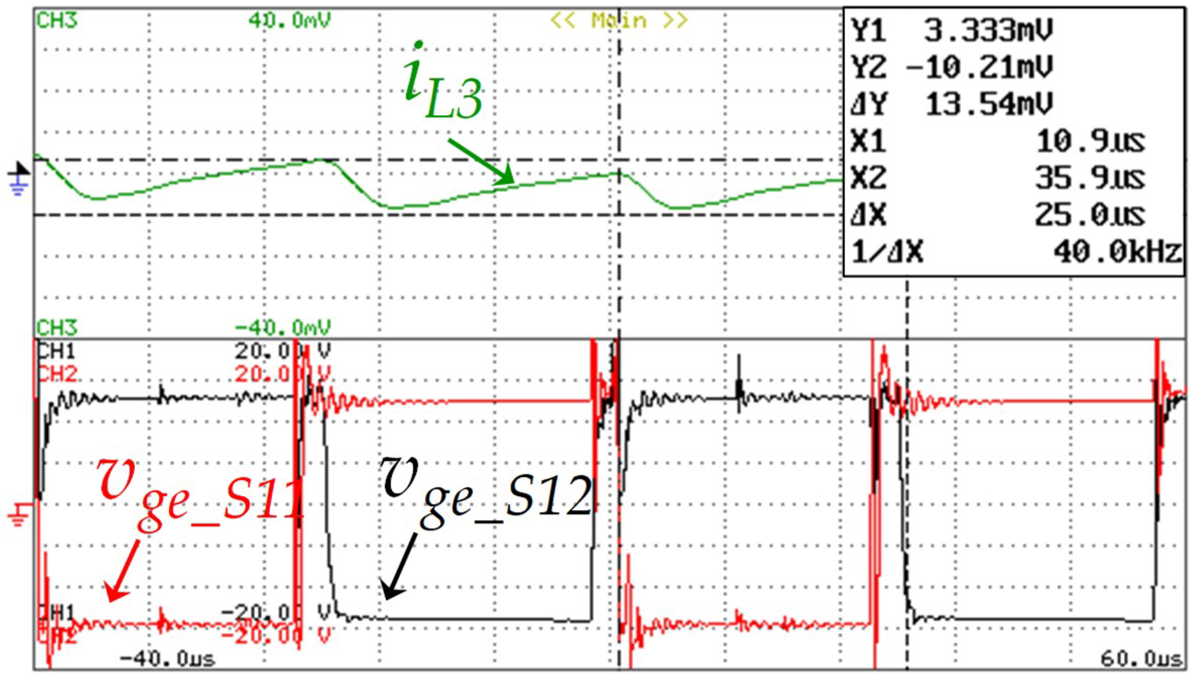
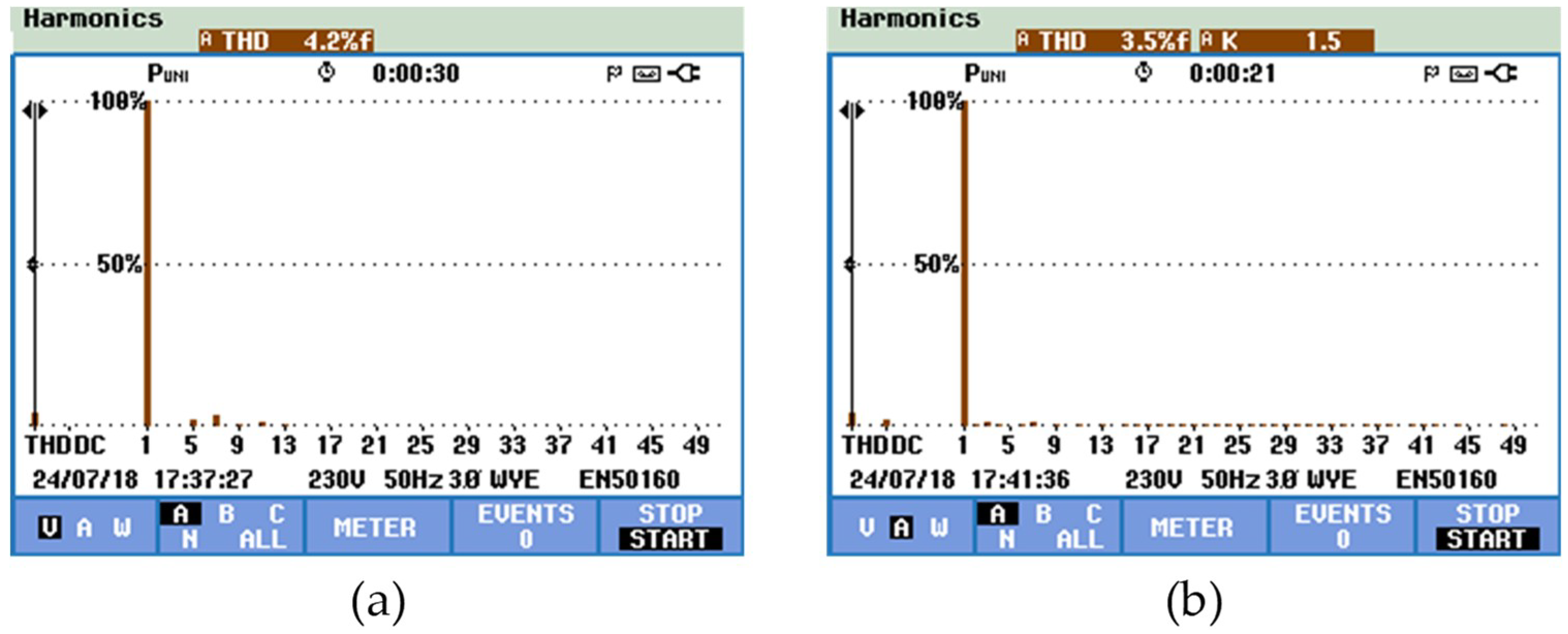
Regarding the battery-side converter, the same modulation technique implemented in the G2V operation mode was used, namely the application of two 180° phase-shifted carrier signal. This strategy was adopted to reduce the ripple amplitude of the batteries current. In this sense, Figure 24 shows the current ripple in the inductor L3 according to the gate-emitter voltages, vge_S11 and vge_S12, of the IGBTs S11, S12. It is important to note that during this operation mode, the IGBTs S9 and S10 are always off, reason why they are not shown in the figure. As it can be seen, the measured current ripple in the inductor L3 was 0.13 A for a frequency of 40 kHz, which is twice of the switching frequency. According to this result, when the IGBT S9 or the IGBT S10 is on, the inductor stores energy and during the state transition of one the IGBTs, the inductor releases this energy. Using the power quality analyzer, in Figure 25a,b, the harmonic spectrum of the power grid voltage and the EVBC current is shown, measured THD% of 4.2% and 3.5%, respectively. These figures were obtained employing a Fluke 435 power quality analyzer, and the high value of THD in the power grid voltage is caused by distorted voltage drop in the line impedance, which is produced by distorted current consumed by several nonlinear loads connected to the electrical installation.
5. Conclusions
A novel on-board bidirectional EV battery charger (EVBC) was presented. It is constituted by a grid-side converter capable to operate with five voltage levels, and by a battery-side converter capable to operate with three voltage levels. The distinct voltage levels for both converters are obtained using a split DC-link. In order to ensure power quality features, the proposed EVBC operates with grid-side current controlled to improve power factor, and to preserve the battery lifetime the EVBC operates with battery-side controlled current or voltage. Throughout the paper is described the proposed hardware topology, the discrete-time predictive control algorithms used for the grid-side converter and for the battery-side converter, the developed full-scale laboratorial prototype of the EVBC, and the foremost experimental results considering operating modes for smart grids. The obtained results allow validating the key contributions of the paper, mainly, in terms of the bidirectional operation of the novel EVBC based on a multilevel topology. As the EVBC is controlled targeting the EV incorporation into smart grids, the grid-to-vehicle (G2V) and vehicle-to-grid (V2G) operation modes are discussed and evaluated.
Author Contributions
All authors contributed equally to the conceptualization and writing of the paper.
Funding
This work has been supported by COMPETE: POCI-01-0145-FEDER-007043 and FCT—Fundação para a Ciência e Tecnologia within the Project Scope: UID/CEC/00319/2013. This work is financed by the ERDF—European Regional Development Fund through the Operational Programme for Competitiveness and Internationalisation—COMPETE 2020 Programme, and by National Funds through the Portuguese funding agency, FCT—Fundação para a Ciência e a Tecnologia, within project SAICTPAC/0004/2015—POCI—01-0145-FEDER-016434. This work is part of the FCT project 0302836 NORTE-01-0145-FEDER-030283.
Conflicts of Interest
The authors declare no conflict of interest.
References
- Idaho National Laboratory. Charging and Driving Behavior of Nissan Leaf Drivers in the EV Project with Access to Workplace Charging; EV Project; Idaho National Laboratory: Idaho Falls, ID, USA, 2014; pp. 1–4.
- Matthé, R.; Eberle, U. The Voltec System—Energy Storage and Electric Propulsion. In Lithium-Ion Batteries—Advances and Applications; Elsevier: Amsterdam, The Netherlands, 2014; pp. 151–176. [Google Scholar]
- Robledo, C.B.; Oldenbroek, V.; Abbruzzese, F.; van Wijk, A.J.M. Integrating a hydrogen fuel cell electric vehicle with vehicle-to-grid technology, photovoltaic power and a residential building. Appl. Energy 2018, 215, 615–629. [Google Scholar] [CrossRef]
- Boulanger, A.G.; Chu, A.C.; Maxx, S.; Waltz, D.L. Vehicle Electrification: Status and Issues. Proc. IEEE 2011, 99, 1116–1138. [Google Scholar] [CrossRef] [Green Version]
- Rajashekara, K. Present Status and Future Trends in Electric Vehicle Propulsion Technologies. IEEE J. Emerg. Sel. Top. Power Electron. 2013, 1, 3–10. [Google Scholar] [CrossRef]
- Milberg, J.; Schlenker, A. Plug into the Future. IEEE Power Energy Mag. 2011, 9, 56–65. [Google Scholar] [CrossRef]
- Monteiro, V.; Ferreira, J.C.; Melendez, A.A.N.; Couto, C.; Afonso, J.L. Experimental Validation of a Novel Architecture Based on a Dual-Stage Converter for Off-Board Fast Battery Chargers of Electric Vehicles. IEEE Trans. Veh. Technol. 2018, 67, 1000–1011. [Google Scholar] [CrossRef]
- Basu, M.; Gaughan, K.; Coyle, E. Harmonic distortion caused by EV battery chargers in the distribution systems network and its remedy. In Proceedings of the International Conference UPEC—Universities Power Engineering Conference, Bristol, UK, 6–8 September 2004; pp. 869–873. [Google Scholar]
- Monteiro, V.; Pinto, J.G.; Afonso, J.L. Operation Modes for the Electric Vehicle in Smart Grids and Smart Homes: Present and Proposed Modes. IEEE Trans. Veh. Technol. 2016, 65, 1007–1020. [Google Scholar] [CrossRef] [Green Version]
- Kisacikoglu, M.C.; Ozpineci, B.; Tolbert, L.M. Examination of a PHEV Bidirectional Charger System for V2G Reactive Power Compensation. In Proceedings of the IEEE APEC Applied Power Electronics Conference and Exposition, Palm Springs, CA, USA, 21–25 February 2010; pp. 458–465. [Google Scholar]
- Monteiro, V.; Ferreira, J.C.; Meléndez, A.A.N.; Afonso, J.L. Electric Vehicles On-Board Battery Charger for the Future Smart Grids. In Technological Innovation for the Internet of Things, 1st ed.; Camarinha-Matos, L.M., Tomic, S., Graça, P., Eds.; Springer: Berlin, Germany, 2013; Chapter 38; pp. 351–358. [Google Scholar]
- Multin, M.; Allerding, F.; Schmeck, H. Integration of Electric Vehicles in Smart Homes—An ICT-based Solution for V2G Scenarios. In Proceedings of the IEEE ISGT PES Innovative Smart Grid Technologies, Washington, DC, USA, 16–20 January 2012; pp. 1–8. [Google Scholar]
- Wong, N.; Kazerani, M. A Review of Bidirectional On-Board Charger Topologies for Plug-In Vehicles. In Proceedings of the IEEE CCECE Canadian Conference on Electrical and Computer Engineering, Montreal, QC, Canada, 29 April–2 May 2012; pp. 1–6. [Google Scholar]
- Mei, J.; Xiao, B.; Shen, K.; Tolbert, L.M.; Zheng, J.Y. Modular Multilevel Inverter with new Modulation Method and its Application to Photovoltaic Grid-Connected Generator. IEEE Trans. Power Electron. 2013, 28, 5063–5073. [Google Scholar] [CrossRef]
- Tolbert, L.M.; Peng, F.Z.; Habetler, T.G. Multilevel Converters for Large Electric Drives. IEEE Trans. Ind. Appl. 1999, 35, 36–44. [Google Scholar] [CrossRef]
- Wang, H.; Kou, L.; Liu, Y.-F.; Sen, P.C. A New Six-Switch Five-Level Active Neutral Point Clamped Inverter for PV Applications. IEEE Trans. Power Electron. 2017, 32, 6700–6715. [Google Scholar] [CrossRef]
- Monteiro, V.; Meléndez, A.A.N.; Afonso, J.L. Novel Single-Phase Five-Level VIENNA-Type Rectifier with Model Predictive Current Control. In Proceedings of the IEEE IECON Industrial Electronics Conference, Beijing, China, 29 October–1 November 2017; pp. 6413–6418. [Google Scholar]
- Grbovic, P.; Lidozzi, A.; Solero, L.; Crescimbini, F. Five-Level Unidirectional T-Rectifier for High Speed Gen-Set Applications. IEEE Trans. Ind. Appl. 2016, 52, 1642–1651. [Google Scholar] [CrossRef]
- Monteiro, V.; Ferreira, J.C.; Meléndez, A.A.N.; Afonso, J.L. Model Predictive Control Applied to an Improved Five-Level Bidirectional Converter. IEEE Trans. Ind. Electron. 2016, 63, 5879–5890. [Google Scholar] [CrossRef] [Green Version]
- Monteiro, V.; Meléndez, A.A.N.; Ferreira, J.C.; Couto, C.; Afonso, J.L. Experimental Validation of a Proposed Single-Phase Five-Level Active Rectifier Operating with Model Predictive Current Control. In Proceedings of the IEEE IECON Industrial Electronics Conference, Yokohama, Japan, 9–12 November 2015; pp. 3939–3944. [Google Scholar]
- Mokhberdoran, A.; Ajami, A. Symmetric and Asymmetric Design and Implementation of New Cascaded Multilevel Inverter Topology. IEEE Trans. Power Electron. 2014, 29, 6712–6724. [Google Scholar] [CrossRef]
- Elsheikh, M.G.; Ahmed, M.E.; Abdelkarem, E.; Orabi, M. Single-Phase Five-Level Inverter with Less Number of Power Elements. In Proceedings of the IEEE INTELEC International Telecommunications Energy Conference, Orlando, FL, USA, 5–9 February 2012; pp. 1–8. [Google Scholar]
- Loukriz, A.H.; Dudley, S.; Quinlan, T.; Walker, S.D. Experimental Realization of a Single-Phase Five Level Inverter for PV Applications. In Proceedings of the IEEE COMPEL Control and Modeling for Power Electronics, Trondheim, Norway, 27–30 June 2016; pp. 1–6. [Google Scholar]
- Wang, K.; Xu, L.; Zheng, Z.; Li, Y. Capacitor Voltage Balancing of a Five-Level ANPC Converter Using Phase-Shifted PWM. IEEE Trans. Power Electron. 2015, 30, 1147–1156. [Google Scholar] [CrossRef]
- Monteiro, V.; Pinto, J.G.; Sousa, T.J.C.; Meléndez, A.A.N.; Afonso, J.L. A Novel Single-Phase Five-Level Active Rectifier for On-Board EV Battery Chargers. In Proceedings of the IEEE ISIE International Symposium on Industrial Electronics, Edinburgh, UK, 19–21 June 2017; Volume 4, pp. 582–587. [Google Scholar]
- Rosas-Caro, J.C.; Ramírez, J.M.; García-Vite, P.M. Novel DC-DC Multilevel Boost Converter. In Proceedings of the IEEE Power Electronics Specialists Conference, Rhodes, Greece, 15–19 June 2008; pp. 2146–2151. [Google Scholar]
- Zhang, F.; Peng, F.Z.; Qian, Z. Study of the Multilevel Converters in DC-DC Applications. In Proceedings of the IEEE Annual Power Electronics Specialists Conference, Aachen, Germany, 20–25 June 2004. [Google Scholar]
- Lee, P.; Lee, Y.; Cheng, D.K.W. Steady-state analysis of an interleaved boost converter with coupled inductors. IEEE Trans. Ind. Electron. 2000, 47, 787–795. [Google Scholar] [CrossRef]
- Jiang, W.; Fahimi, B. Phase-Shift Controlled Multilevel Bidirectional DC/DC Converter: A Novel Solution to Battery Charge Equalization in Fuel Cell Vehicle. In Proceedings of the IEEE Vehicle Power and Propulsion Conference, Arlington, TX, USA, 9–12 September 2007; pp. 587–590. [Google Scholar]
Figure 1.
Internal constitution of a conventional on-board electric vehicle battery charger (EVBC).

Figure 2.
Topology of the proposed on-board electric vehicle battery charger (EVBC).

Figure 3.
Operation stages for the grid-side converter during the operation as active rectifier: (a) vcv_AC = 0; (b) vcv_AC = +vdc/2; (c) vcv_AC = +vdc; (d) vcv_AC = 0; (e) vcv_AC = −vdc/2; (f) vcv_AC = −vdc.
Figure 3.
Operation stages for the grid-side converter during the operation as active rectifier: (a) vcv_AC = 0; (b) vcv_AC = +vdc/2; (c) vcv_AC = +vdc; (d) vcv_AC = 0; (e) vcv_AC = −vdc/2; (f) vcv_AC = −vdc.

Figure 4.
Operation stages for the grid-side converter during the operation as grid-tied inverter: (a) vcv_AC = 0; (b) vcv_AC = +vdc/2; (c) vcv_AC = +vdc; (d) vcv_AC = 0; (e) vcv_AC = −vdc/2; (f) vcv_AC = −vdc.
Figure 4.
Operation stages for the grid-side converter during the operation as grid-tied inverter: (a) vcv_AC = 0; (b) vcv_AC = +vdc/2; (c) vcv_AC = +vdc; (d) vcv_AC = 0; (e) vcv_AC = −vdc/2; (f) vcv_AC = −vdc.

Figure 5.
Modified pulse-width modulation (PWM) strategy for the grid-side converter during the operation as active rectifier or as grid-tied inverter.
Figure 5.
Modified pulse-width modulation (PWM) strategy for the grid-side converter during the operation as active rectifier or as grid-tied inverter.

Figure 6.
Operation stages for the battery-side converter during the operation as a buck-type converter: (a) The stored energy in L3, L4 is released to the batteries; (b) L3, L4 and the batteries stores energy from C1; (c) L3, L4 and the batteries stores energy from C2; (d) L3, L4 and the batteries store energy from C1, C2.

Figure 7.
Operation stages for the battery-side converter during the operation as a boost-type converter: (a) L3, L4 stores energy from the batteries; (b) C2 stores energy from the batteries and L3, L4; (c) C1 stores energy from the batteries and L3, L4; (d) C1, C2 stores energy from the batteries and L3, L4.

Figure 8.
Three-dimensional modeling of the proposed on-board EVBC.

Figure 9.
Laboratorial prototype of the developed EVBC.

Figure 10.
Internal volume distribution of the developed on-board EVBC.

Figure 11.
Laboratory setup used to obtain the experimental results.

Figure 12.
Experimental results during the initial stage of the electric vehicle (EV) battery charging process: EV battery current (ibat: 1 A/div); DC-link voltages of both capacitors (vdc1: 20 V/div, vdc2: 20 V/div); EVBC current (iev: 2 A/div).
Figure 12.
Experimental results during the initial stage of the electric vehicle (EV) battery charging process: EV battery current (ibat: 1 A/div); DC-link voltages of both capacitors (vdc1: 20 V/div, vdc2: 20 V/div); EVBC current (iev: 2 A/div).

Figure 13.
Experimental results in grid-to-vehicle (G2V) mode showing the EVBC current (iev: 5 A/div), the grid voltage (vg: 100 V/div), a detail of zero crossing between the current and the voltage (iev, vg), and the DC-link voltages ripple in both capacitors (Δvdc1: 5 V/div, Δvdc2: 5 V/div).
Figure 13.
Experimental results in grid-to-vehicle (G2V) mode showing the EVBC current (iev: 5 A/div), the grid voltage (vg: 100 V/div), a detail of zero crossing between the current and the voltage (iev, vg), and the DC-link voltages ripple in both capacitors (Δvdc1: 5 V/div, Δvdc2: 5 V/div).

Figure 14.
Experimental results during the G2V operation mode: Gate-emitter voltage of the grid-side insulated-gate bipolar transistors (IGBTs) (S1, S2, S3, S4, S5, S6: 5 V/div); Output digital signal of the phase-locked loop (PLL) (vPLL: 150 V/div).
Figure 14.
Experimental results during the G2V operation mode: Gate-emitter voltage of the grid-side insulated-gate bipolar transistors (IGBTs) (S1, S2, S3, S4, S5, S6: 5 V/div); Output digital signal of the phase-locked loop (PLL) (vPLL: 150 V/div).

Figure 15.
Experimental results showing the current in the inductor L3 (iL3: 0.1 A/div) and the gate-emitter voltage of the IGBTs S9 and S10 (vge_s9: 5 V/div and vge_10: 5 V/div) during a time interval of 100 µs.
Figure 15.
Experimental results showing the current in the inductor L3 (iL3: 0.1 A/div) and the gate-emitter voltage of the IGBTs S9 and S10 (vge_s9: 5 V/div and vge_10: 5 V/div) during a time interval of 100 µs.

Figure 16.
Experimental results in x-y mode showing the EVBC current (iev: 5 A/div) in function of the power grid voltage (vg: 100 V/div).
Figure 16.
Experimental results in x-y mode showing the EVBC current (iev: 5 A/div) in function of the power grid voltage (vg: 100 V/div).

Figure 17.
Experimental results in x-y mode showing the DC-link voltage ripple (Δvdc1: 5 V/div, Δvdc2: 5 V/div) (y-axis) and the voltage levels produced by the grid-side converter (vcv_AC: 50 V/div) (y-axis), both in function of the power grid voltage (vg: 100 V/div) (x-axis).
Figure 17.
Experimental results in x-y mode showing the DC-link voltage ripple (Δvdc1: 5 V/div, Δvdc2: 5 V/div) (y-axis) and the voltage levels produced by the grid-side converter (vcv_AC: 50 V/div) (y-axis), both in function of the power grid voltage (vg: 100 V/div) (x-axis).

Figure 18.
Experimental results in G2V mode of the total harmonic distortion and spectral analysis: (a) power grid voltage (vg); and (b) EVBC current (iev).
Figure 18.
Experimental results in G2V mode of the total harmonic distortion and spectral analysis: (a) power grid voltage (vg); and (b) EVBC current (iev).

Figure 19.
Experimental results of the temperature measurements during G2V operation mode: (a) overall thermal distribution of the developed EVBC prototype; (b) temperature at the IGBT S9; and (c) temperature at the IGBT S11.
Figure 19.
Experimental results of the temperature measurements during G2V operation mode: (a) overall thermal distribution of the developed EVBC prototype; (b) temperature at the IGBT S9; and (c) temperature at the IGBT S11.

Figure 20.
Experimental results showing the modulation technique applied to the IGBTs S7 and S8, namely, the reference signals adopted for the modulation (refs7: 1 V/div, refs8: 1 V/div) and the voltage gate-emitter of the respective IGBT (vge_s7: 5 V/div and vge_s8: 5 V/div).
Figure 20.
Experimental results showing the modulation technique applied to the IGBTs S7 and S8, namely, the reference signals adopted for the modulation (refs7: 1 V/div, refs8: 1 V/div) and the voltage gate-emitter of the respective IGBT (vge_s7: 5 V/div and vge_s8: 5 V/div).

Figure 21.
Experimental results during vehicle-to-grid (V2G) operation mode: Gate-emitter voltage of the grid-side IGBTs (S1, S2, S3, S4, S7, S8: 5 V/div), and output digital signal of the PLL (vPLL: 150 V/div).
Figure 21.
Experimental results during vehicle-to-grid (V2G) operation mode: Gate-emitter voltage of the grid-side IGBTs (S1, S2, S3, S4, S7, S8: 5 V/div), and output digital signal of the PLL (vPLL: 150 V/div).

Figure 22.
Experimental results in V2G operation mode showing the EVBC current (iev: 5 A/div), the power grid voltage (vg: 50 V/div), the voltage levels produced by the grid-side converter (vcv_AC: 100 V/div) and the DC-link voltage of both capacitors (vdc1: 20 V/div, vdc2: 20 V/div).
Figure 22.
Experimental results in V2G operation mode showing the EVBC current (iev: 5 A/div), the power grid voltage (vg: 50 V/div), the voltage levels produced by the grid-side converter (vcv_AC: 100 V/div) and the DC-link voltage of both capacitors (vdc1: 20 V/div, vdc2: 20 V/div).

Figure 23.
Experimental results in V2G operation mode showing the EVBC current (iev: 5 A/div), the grid voltage (vg: 50 V/div), a detail of zero crossing between the current and the voltage (iev, vg), and the DC-link voltages ripple in both capacitors (Δvdc1: 2 V/div, Δvdc2: 2 V/div).
Figure 23.
Experimental results in V2G operation mode showing the EVBC current (iev: 5 A/div), the grid voltage (vg: 50 V/div), a detail of zero crossing between the current and the voltage (iev, vg), and the DC-link voltages ripple in both capacitors (Δvdc1: 2 V/div, Δvdc2: 2 V/div).

Figure 24.
Experimental results showing the current in the inductor L3 (iL3: 0.1 A/div) and the gate-emitter voltage of the IGBTs S11 and S12 (vge_s11: 5 V/div and vge_12: 5 V/div) during a time interval of 100 µs.
Figure 24.
Experimental results showing the current in the inductor L3 (iL3: 0.1 A/div) and the gate-emitter voltage of the IGBTs S11 and S12 (vge_s11: 5 V/div and vge_12: 5 V/div) during a time interval of 100 µs.

Figure 25.
Experimental results in V2G operation mode of the total harmonic distortion and spectral analysis: (a) Power grid voltage (vg); and (b) EVBC current (iev).
Figure 25.
Experimental results in V2G operation mode of the total harmonic distortion and spectral analysis: (a) Power grid voltage (vg); and (b) EVBC current (iev).


Table 1.
Parameters and specifications of the on-board EVBC.
| Parameter | Value | Unit | |
|---|---|---|---|
| Inductive Passive Filter | L1, L2 | 5 | mH |
| Inductive Passive Filter | L3, L4 | 2.5 | mH |
| Capacitive Passive Filter | C1, C2 | 2.24 | mF |
| Capacitive Passive Filter | C3 | 20 | µF |
| Nominal Input Voltage (grid-side) | vg | 230 ± 10% | V |
| Nominal Grid Frequency | f | 50 ± 1% | Hz |
| Nominal Input Current (grid-side) | iev | 16 | A |
| Total Harmonic Distortion (grid current) | - | <5% | - |
| Total Power Factor | - | 1 | - |
| Nominal DC-link Voltage | vdc | 400 | V |
| Nominal Output Voltage (battery-side) | vbat | 200–400 | V |
| Nominal Output Current (battery-side) | ibat | 10 | A |
| Switching Frequency | fsw | 20 | kHz |
| Sampling Frequency | fs | 40 | kHz |
© 2018 by the authors. Licensee MDPI, Basel, Switzerland. This article is an open access article distributed under the terms and conditions of the Creative Commons Attribution (CC BY) license (http://creativecommons.org/licenses/by/4.0/).
Share and Cite
MDPI and ACS Style
Leite, R.S.; Afonso, J.L.; Monteiro, V. A Novel Multilevel Bidirectional Topology for On-Board EV Battery Chargers in Smart Grids. Energies 2018, 11, 3453. https://0-doi-org.brum.beds.ac.uk/10.3390/en11123453
AMA Style
Leite RS, Afonso JL, Monteiro V. A Novel Multilevel Bidirectional Topology for On-Board EV Battery Chargers in Smart Grids. Energies. 2018; 11(12):3453. https://0-doi-org.brum.beds.ac.uk/10.3390/en11123453
Chicago/Turabian StyleLeite, Rafael S., João L. Afonso, and Vítor Monteiro. 2018. "A Novel Multilevel Bidirectional Topology for On-Board EV Battery Chargers in Smart Grids" Energies 11, no. 12: 3453. https://0-doi-org.brum.beds.ac.uk/10.3390/en11123453
Note that from the first issue of 2016, this journal uses article numbers instead of page numbers. See further details here.