A New Efficient Step-Up Boost Converter with CLD Cell for Electric Vehicle and New Energy Systems

 ,
,  ,
,  , and
, and
Abstract
:1. Introduction
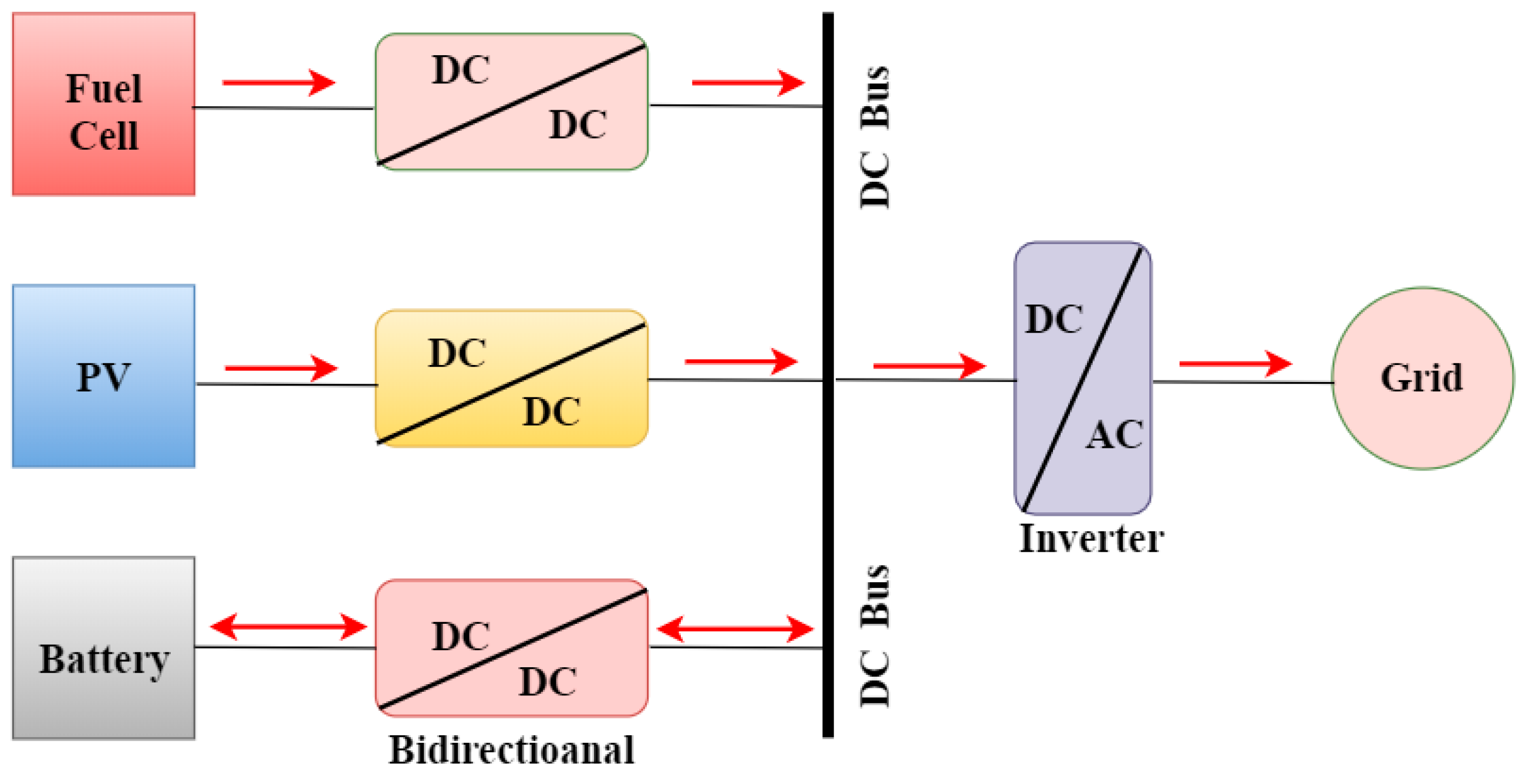
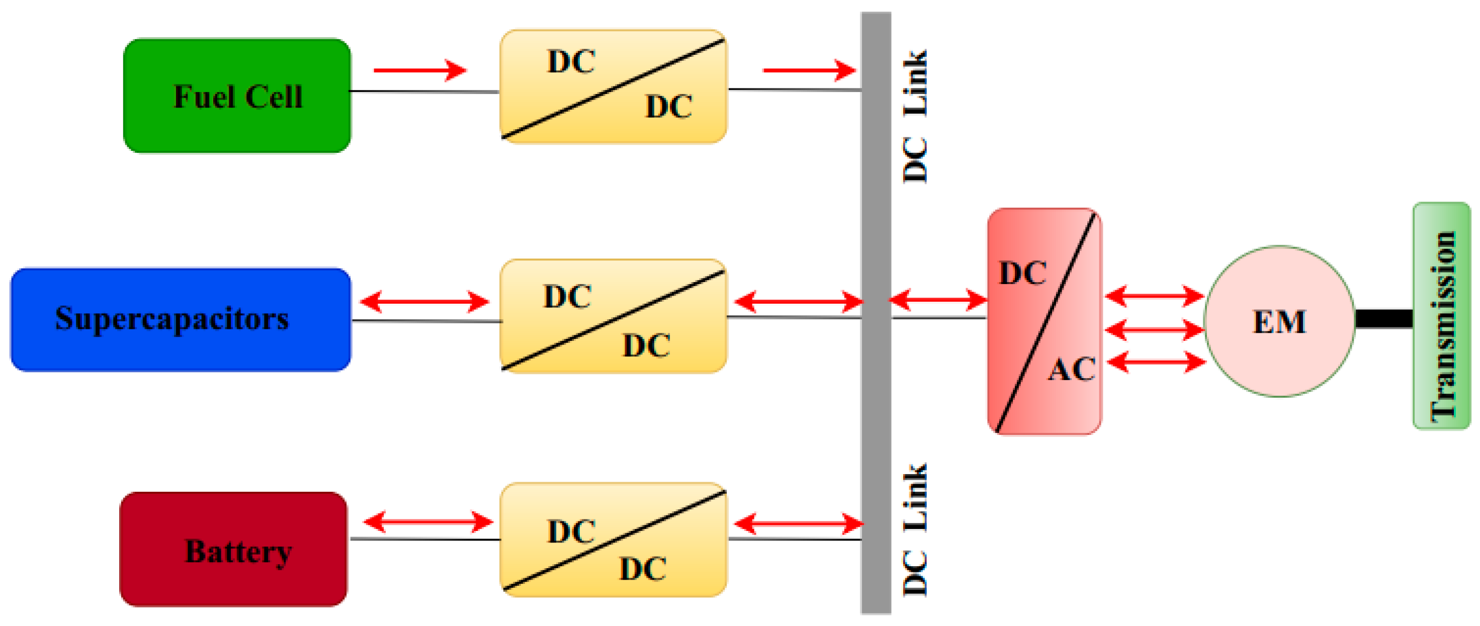
2. Related Work
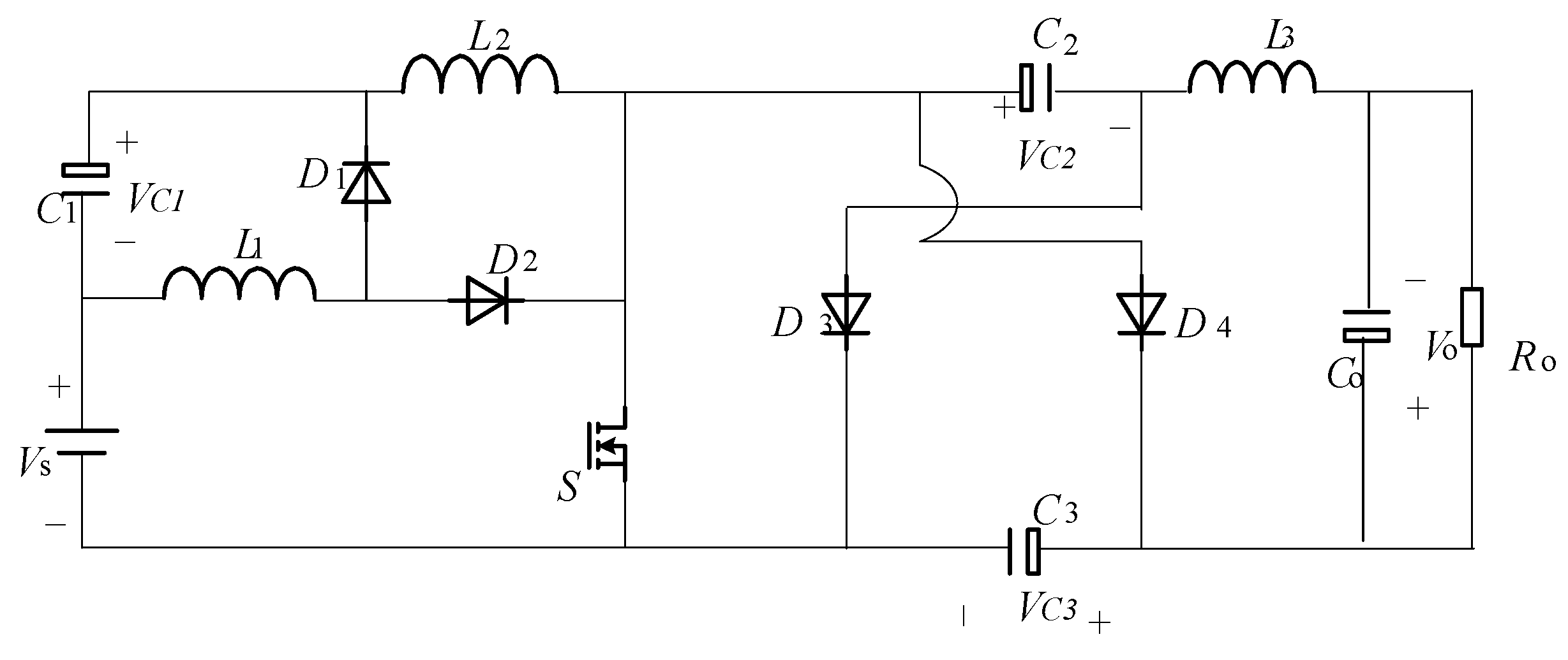
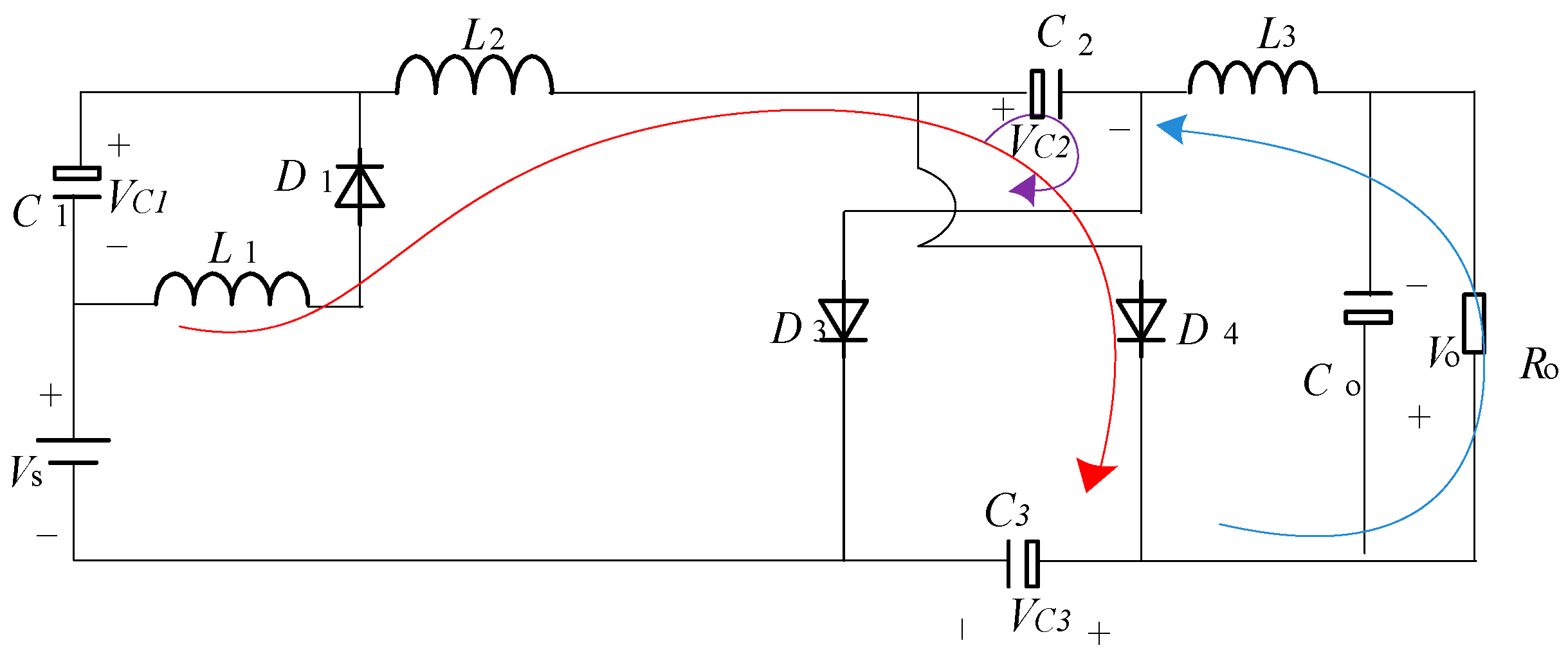
3. Working Method of the Proposed Converter
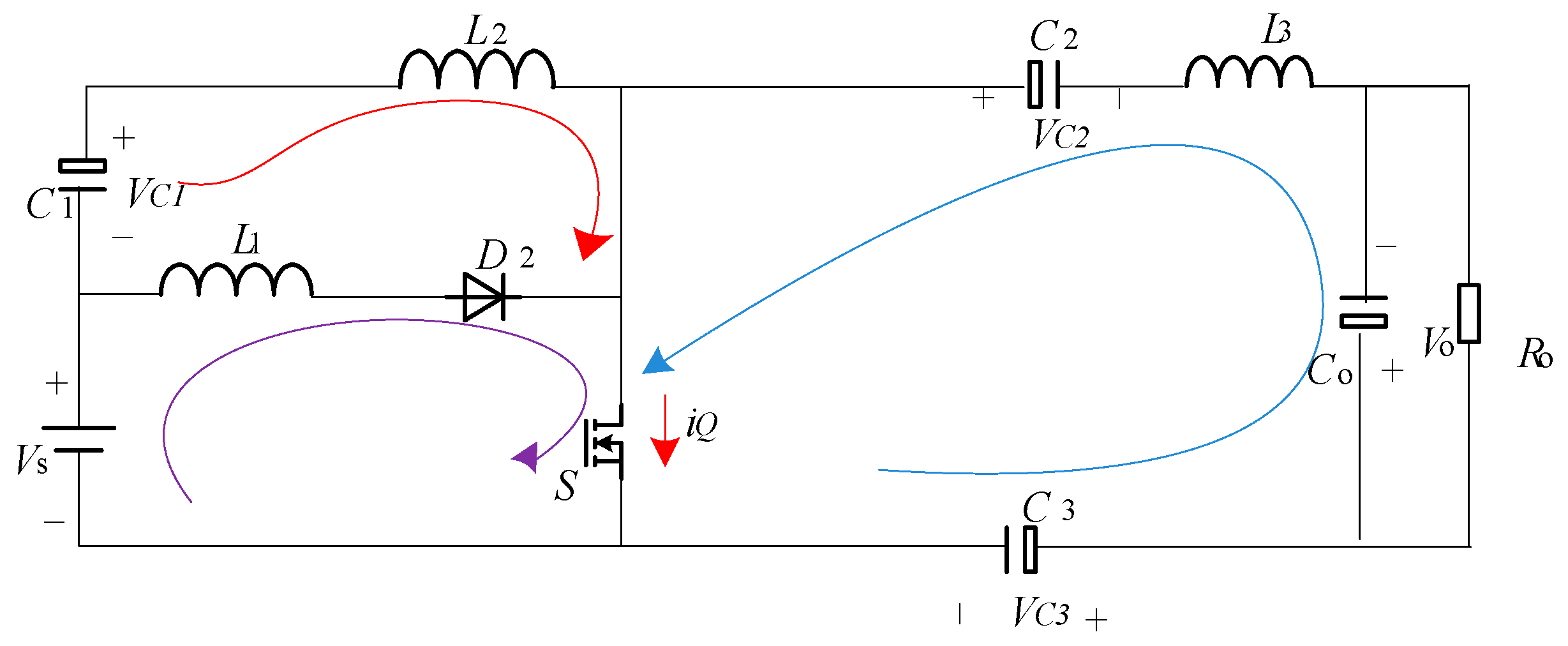
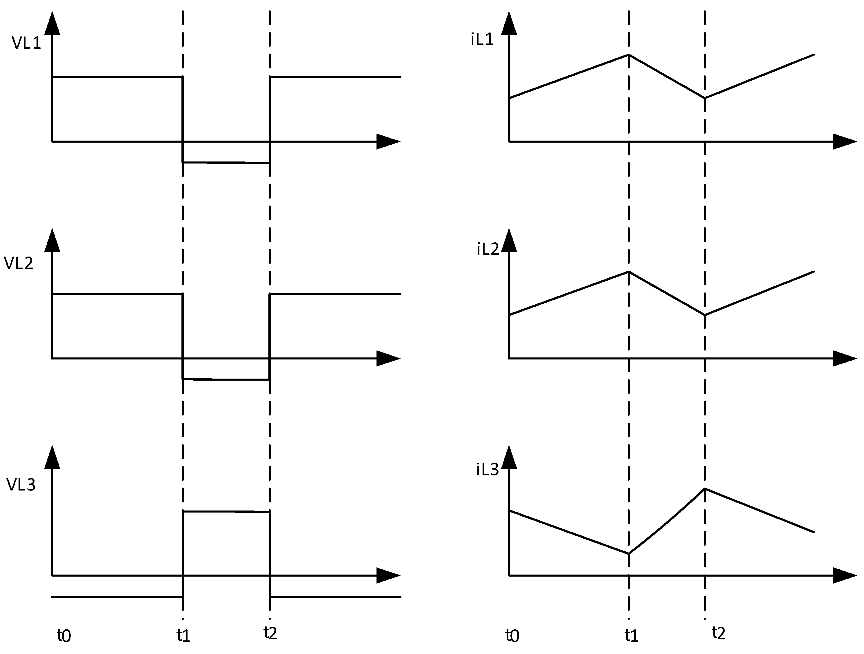
3.1. MOSFET Switch ON State (t0 − t1)
3.2. MOSFET Switch OFF State (t1–t2)
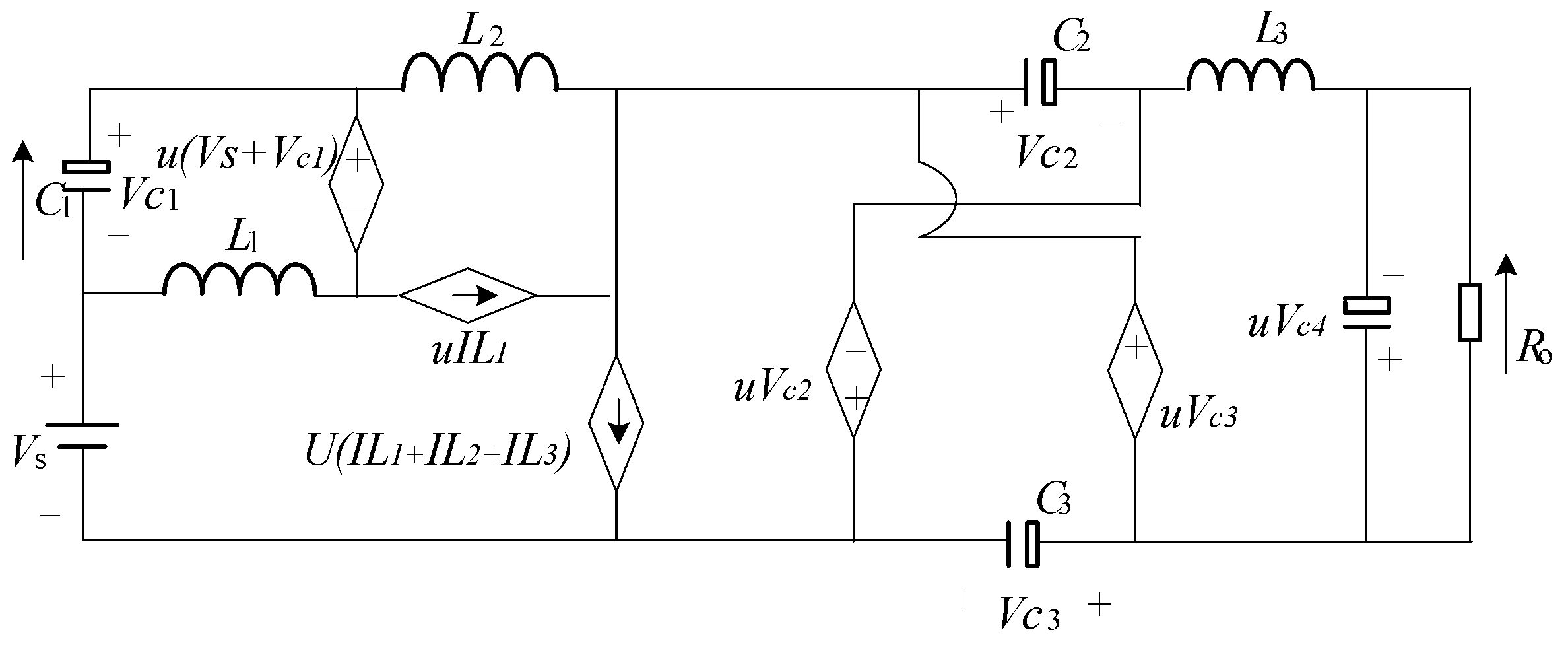
4. Steady-State Analysis of the Proposed Converter
4.1. DC Conversion Ratio
4.2. Dynamic Modeling of the Proposed Converter
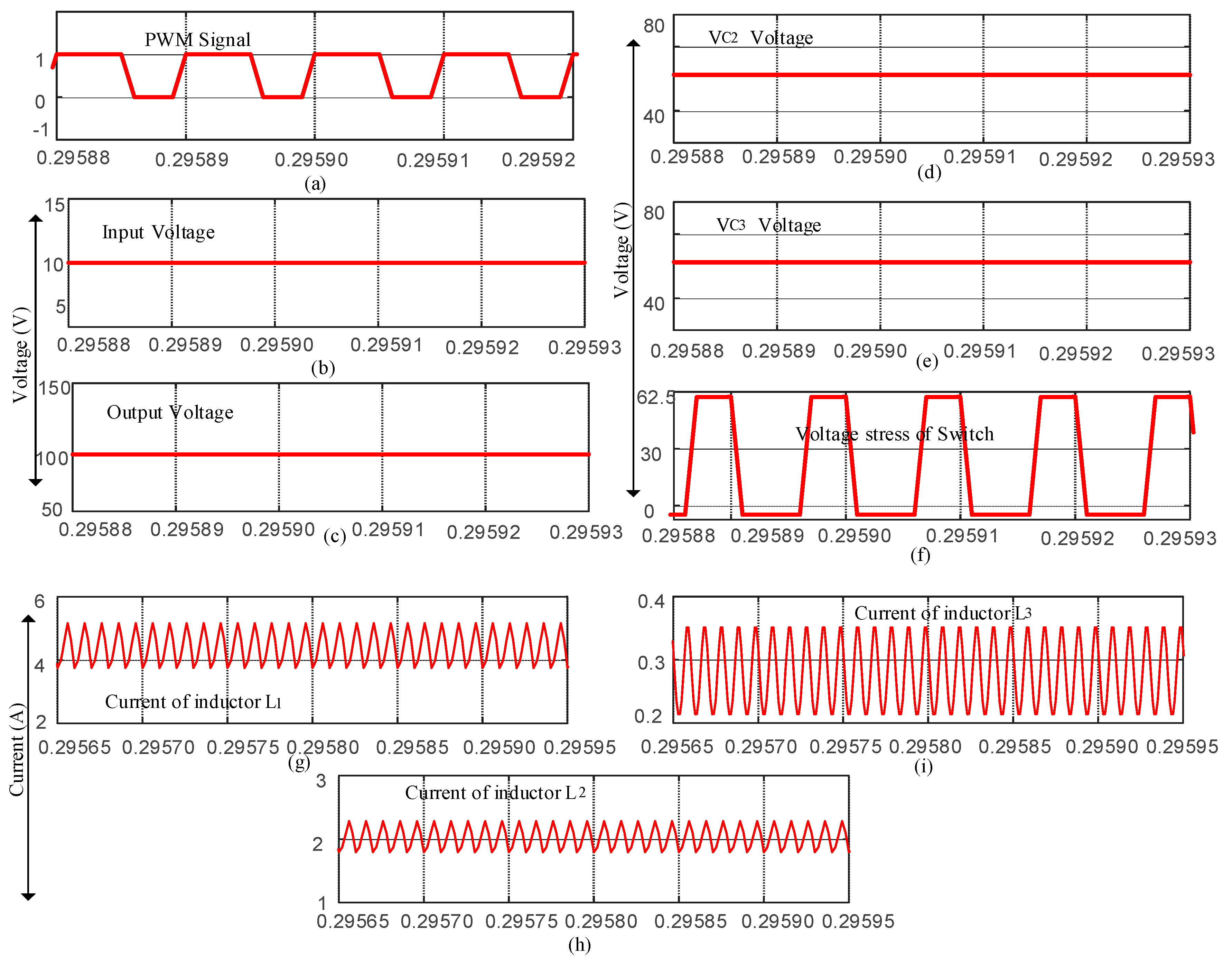
5. Simulation Results & Discussion
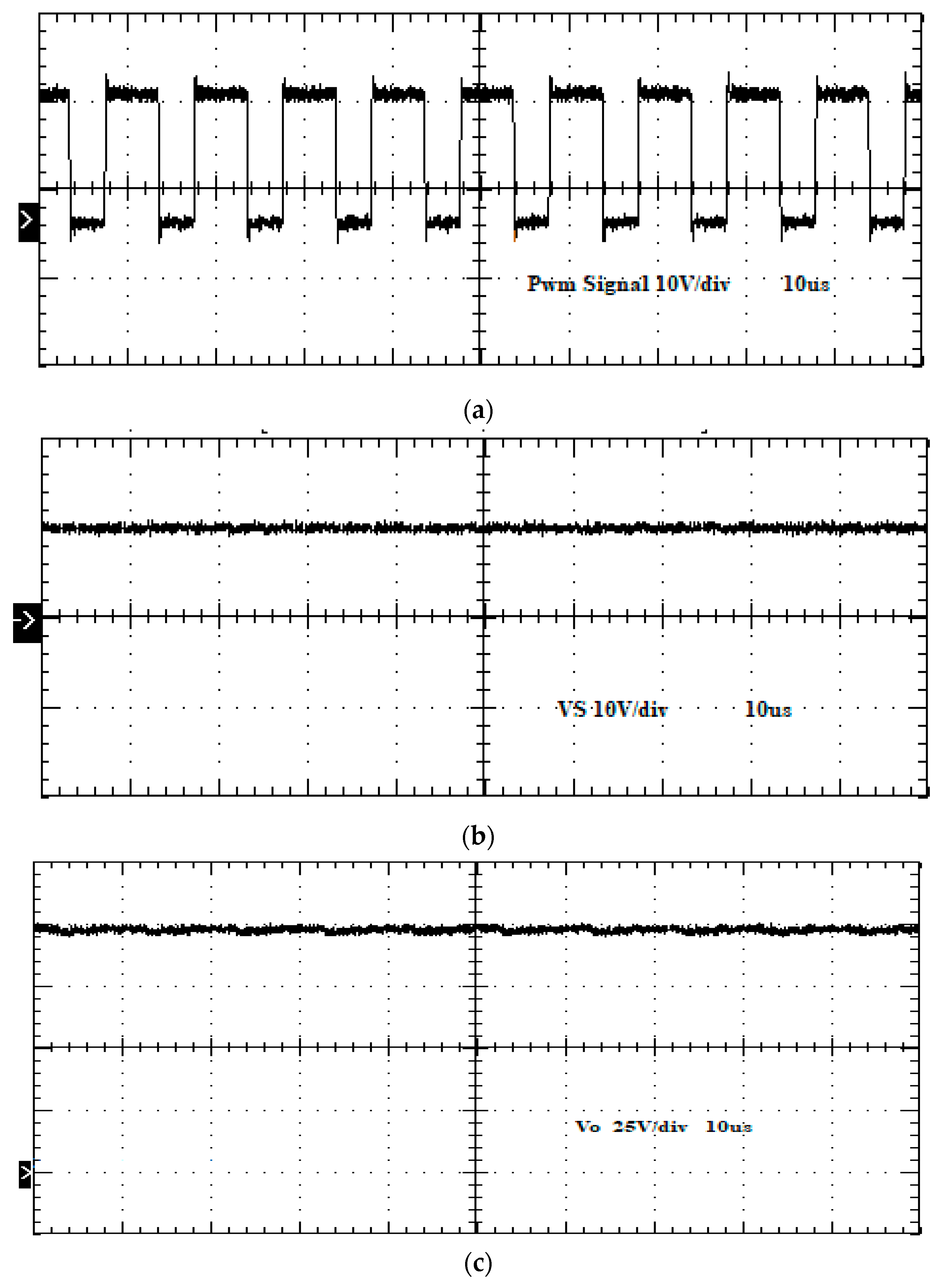
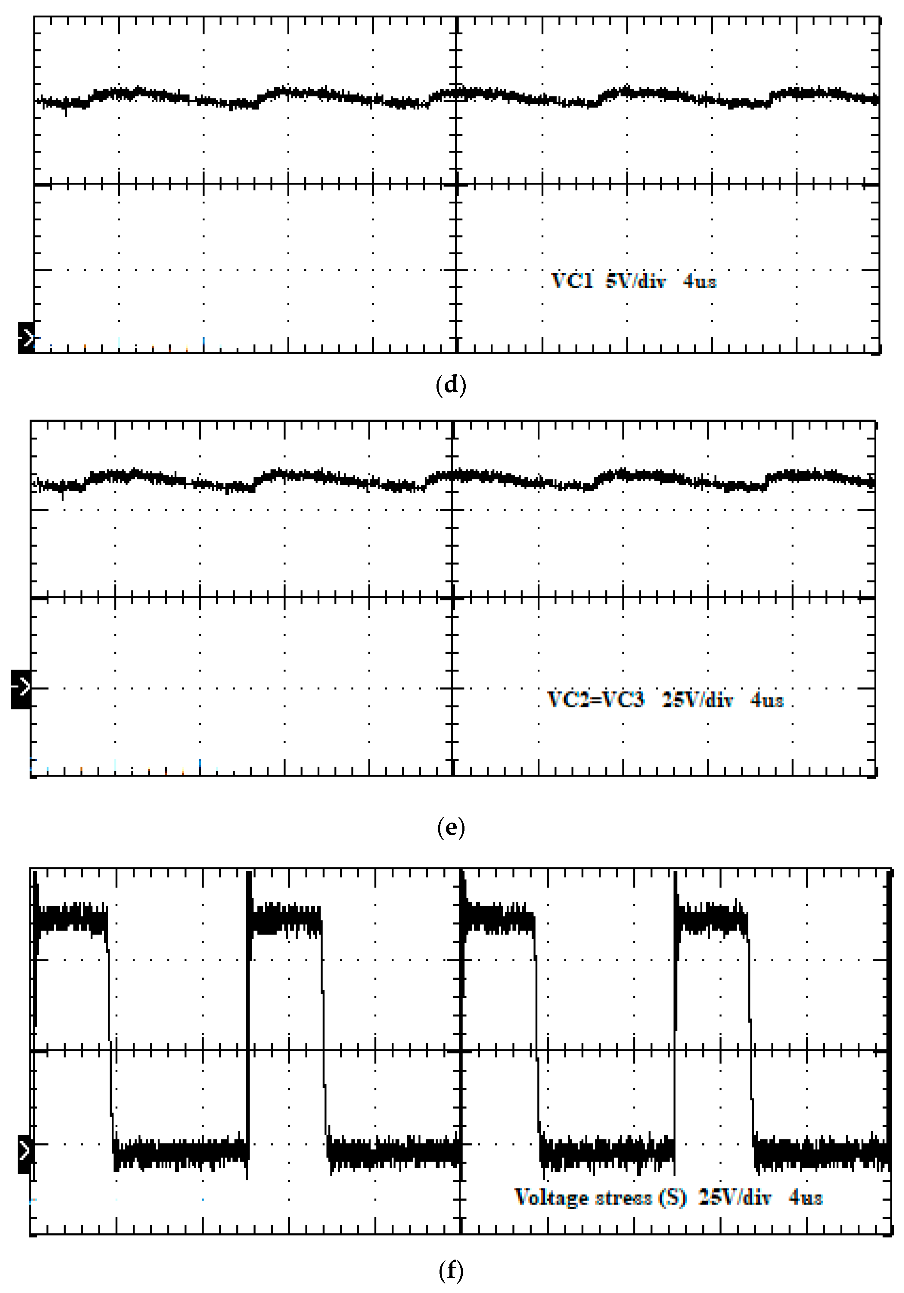
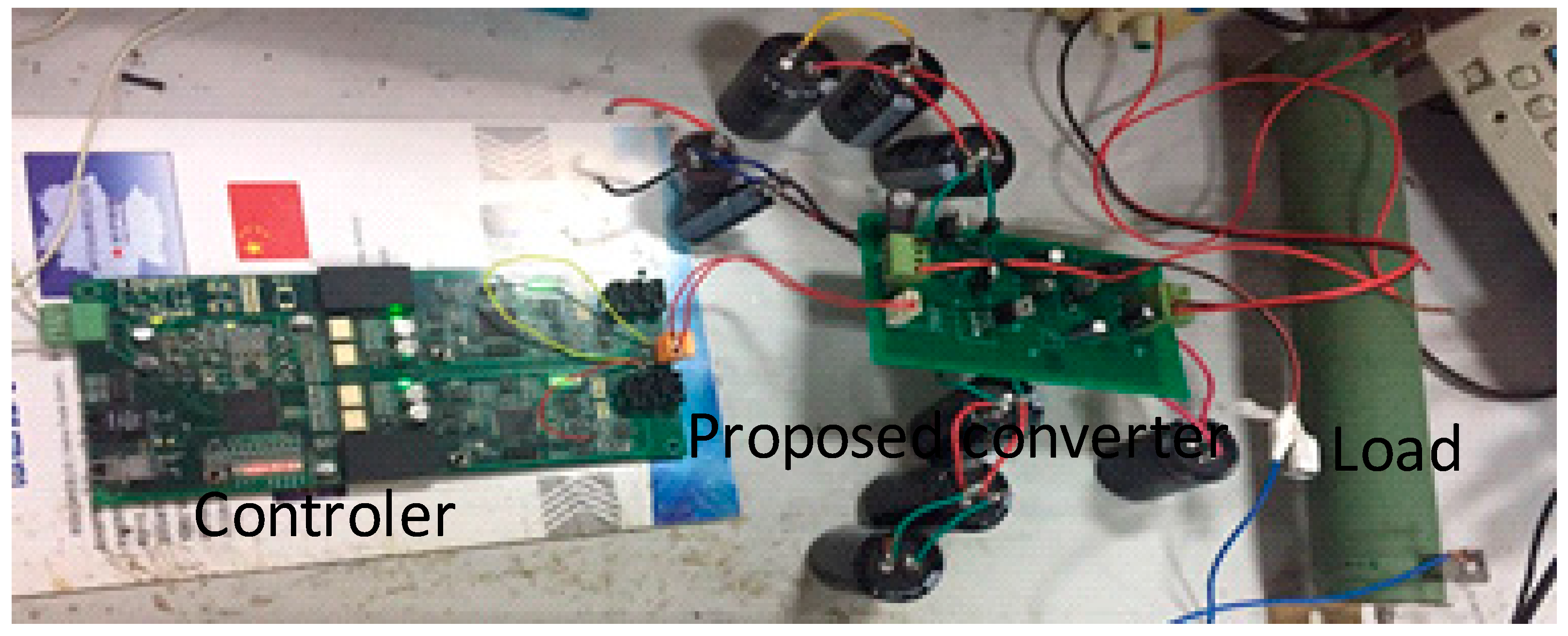
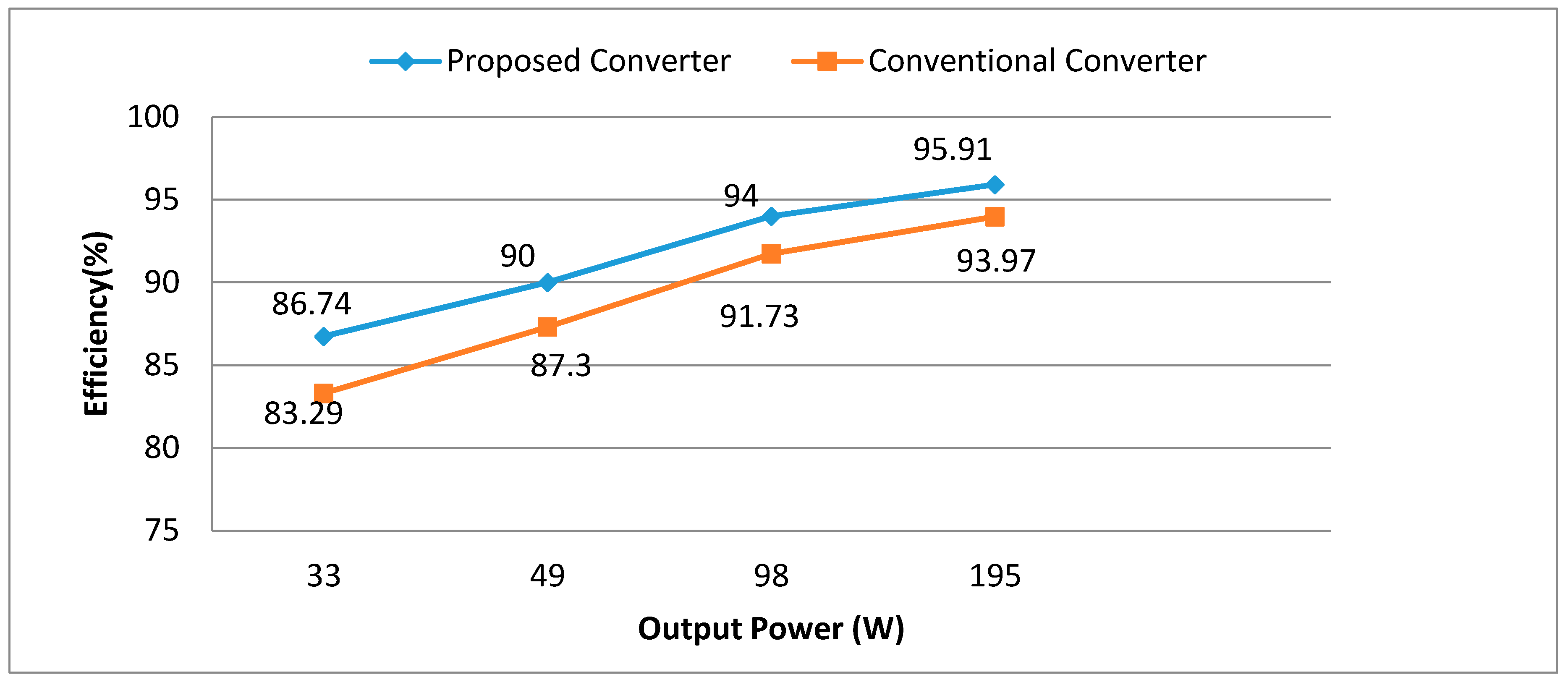
6. Experimental Results & Discussion
7. Conclusions
Author Contributions
Funding
Conflicts of Interest
References
- Ahmad, B.; Kyyra, J.; Martinez, W. Efficiency optimisation of an interleaved high step-up converter. J. Eng. 2019, 2019, 4167–4172. [Google Scholar] [CrossRef]
- Cornea, O.; Andreescu, G.-D.; Muntean, N.; Hulea, D. Bidirectional power flow control in a DC microgrid through a switched-capacitor cell hybrid DC–DC converter. IEEE Trans. Ind. Electron. 2016, 64, 3012–3022. [Google Scholar] [CrossRef]
- Pop-Calimanu, I.-M.; Lica, S.; Popescu, S.; Lascu, D.; Lie, I.; Mirsu, R. A New Hybrid Inductor-Based Boost DC-DC Converter Suitable for Applications in Photovoltaic Systems. Energies 2019, 12, 252. [Google Scholar] [CrossRef] [Green Version]
- Khan, I.; Li, Z.; Xu, Y.; Gu, W. Distributed control algorithm for optimal reactive power control in power grids. Int. J. Electr. Power Energy Syst. 2016, 83, 505–513. [Google Scholar] [CrossRef]
- Shahzad Nazir, M.; Wu, Q.; Li, M. Symmetrical Short-Circuit Parameters Comparison of DFIG–WT. Int. J. Electr. Comput. Eng. Syst. 2017, 8, 77–83. [Google Scholar] [CrossRef] [Green Version]
- Itani, K.; De Bernardinis, A.; Khatir, Z.; Jammal, A.; Oueidat, M. Regenerative braking modeling, control, and simulation of a hybrid energy storage system for an electric vehicle in extreme conditions. IEEE Trans. Transp. Electrif. 2016, 2, 465–479. [Google Scholar] [CrossRef]
- Kouchachvili, L.; Yaïci, W.; Entchev, E. Hybrid battery/supercapacitor energy storage system for the electric vehicles. J. Power Sources 2018, 374, 237–248. [Google Scholar] [CrossRef]
- Akar, F.; Tavlasoglu, Y.; Ugur, E.; Vural, B.; Aksoy, I. A bidirectional nonisolated multi-input DC–DC converter for hybrid energy storage systems in electric vehicles. IEEE Trans. Veh. Technol. 2015, 65, 7944–7955. [Google Scholar] [CrossRef]
- Ren, G.; Ma, G.; Cong, N. Review of electrical energy storage system for vehicular applications. Renew. Sustain. Energy Rev. 2015, 41, 225–236. [Google Scholar] [CrossRef]
- Kim, T.; Feng, D.; Jang, M.; Agelidis, V.G. Common mode noise analysis for cascaded boost converter with silicon carbide devices. IEEE Trans. Power Electron. 2016, 32, 1917–1926. [Google Scholar] [CrossRef]
- Malik, M.Z.; Xu, Q.; Farooq, A.; Chen, G. A new modified quadratic boost converter with high voltage gain. IEICE Electron. Express 2016, 14, 20161176. [Google Scholar] [CrossRef] [Green Version]
- Ellahi, M.; Abbas, G.; Khan, I.; Koola, P.M.; Nasir, M.; Raza, A.; Farooq, U. Recent Approaches of Forecasting and Optimal Economic Dispatch to Overcome Intermittency of Wind and Photovoltaic (PV) Systems: A Review. Energies 2019, 12, 4392. [Google Scholar] [CrossRef] [Green Version]
- Khan, I.; Xu, Y.; Sun, H.; Bhattacharjee, V. Distributed optimal reactive power control of power systems. IEEE Access 2017, 6, 7100–7111. [Google Scholar] [CrossRef]
- García-Sánchez, J.R.; Hernández-Márquez, E.; Ramírez-Morales, J.; Marciano-Melchor, M.; Marcelino-Aranda, M.; Taud, H.; Silva-Ortigoza, R. A Robust Differential Flatness-Based Tracking Control for the “MIMO DC/DC Boost Converter–Inverter–DC Motor” System: Experimental Results. IEEE Access 2019, 7, 84497–84505. [Google Scholar] [CrossRef]
- Farooq, A.; Malik, Z.; Sun, Z.; Chen, G. A Review of non-isolated high step-down Dc-Dc Converters. Int. J. Smart Home 2015, 9, 133–150. [Google Scholar] [CrossRef]
- Thenathayalan, D.; Lee, C.; Park, J.-H. High-order resonant converter topology with extremely low-coupling contactless transformers. IEEE Trans. Power Electron. 2015, 31, 2347–2361. [Google Scholar] [CrossRef]
- Maksimovic, D.; Cuk, S. Switching converters with wide DC conversion range. IEEE Trans. Power Electron. 1991, 6, 151–157. [Google Scholar] [CrossRef]
- Axelrod, B.; Berkovich, Y.; Ioinovici, A. Switched-capacitor/switched-inductor structures for getting transformerless hybrid DC–DC PWM converters. IEEE Trans. Circuits Syst. I Regul. Pap. 2008, 55, 687–696. [Google Scholar] [CrossRef]
- Chen, M.; Li, K.; Hu, J.; Ioinovici, A. Hybrid switched-capacitor quadratic boost converters with very high DC gain and low voltage stress on their semiconductor devices. In Proceedings of the 2016 IEEE Energy Conversion Congress and Exposition (ECCE), Milwaukee, WI, USA, 18–22 September 2016; pp. 1–8. [Google Scholar]
- Lin, B.-R. Investigation of a resonant dc–dc converter for light rail transportation applications. Energies 2018, 11, 1078. [Google Scholar] [CrossRef] [Green Version]
- Lee, S.-W.; Do, H.-L. High step-up coupled-inductor cascade boost DC–DC converter with lossless passive snubber. IEEE Trans. Ind. Electron. 2018, 65, 7753–7761. [Google Scholar] [CrossRef]
- Zhang, G.; Iu, H.H.-C.; Zhang, B.; Li, Z.; Fernando, T.; Chen, S.-Z.; Zhang, Y. An impedance network boost converter with a high-voltage gain. IEEE Trans. Power Electron. 2017, 32, 6661–6665. [Google Scholar] [CrossRef]
- Naderi, A.; Abbaszadeh, K. High step-up DC–DC converter with input current ripple cancellation. IET Power Electron. 2016, 9, 2394–2403. [Google Scholar] [CrossRef]
- Malik, M.Z.; Ali, A.; Xu, Q.; Chen, G. A New Quadratic Boost Converter with Voltage Multiplier Cell: An Analysis and Assessment. Int. J. Smart Home 2016, 10, 281–294. [Google Scholar] [CrossRef]
- Richelli, A.; Colalongo, L.; Tonoli, S.; Kovacs-Vajna, Z.M. A 0.2$-\hbox {1.2} $ V DC/DC Boost Converter for Power Harvesting Applications. IEEE Trans. Power Electron. 2009, 24, 1541–1546. [Google Scholar] [CrossRef]
- Bhaskar, M.S.; Padmanaban, S.; Kulkarni, R.; Blaabjerg, F.; Seshagiri, S.; Hajizadeh, A. Novel LY converter topologies for high gain transfer ratio—A new breed of XY family. In Proceedings of the 4th IET Clean Energy and Technology Conference (CEAT 2016), Kuala Lumpur, Malaysia, 14–15 November 2016. [Google Scholar]
- Maalandish, M.; Hosseini, S.H.; Ghasemzadeh, S.; Babaei, E.; Alishah, R.S.; Jalilzadeh, T. Six-phase interleaved boost dc/dc converter with high-voltage gain and reduced voltage stress. IET Power Electron. 2017, 10, 1904–1914. [Google Scholar] [CrossRef]
- Wang, H.; Li, Z. A PWM LLC type resonant converter adapted to wide output range in PEV charging applications. IEEE Trans. Power Electron. 2017, 33, 3791–3801. [Google Scholar] [CrossRef]
- Leyva-Ramos, J.; Mota-Varona, R.; Ortiz-Lopez, M.G.; Diaz-Saldierna, L.H.; Langarica-Cordoba, D. Control strategy of a quadratic boost converter with voltage multiplier cell for high-voltage gain. IEEE J. Emerg. Sel. Top. Power Electron. 2017, 5, 1761–1770. [Google Scholar] [CrossRef]
- Wu, H.; Zhan, X.; Xing, Y. Interleaved LLC resonant converter with hybrid rectifier and variable-frequency plus phase-shift control for wide output voltage range applications. IEEE Trans. Power Electron. 2016, 32, 4246–4257. [Google Scholar] [CrossRef]
- Malik, M.Z.; Farooq, A.; Ali, A.; Chen, G. A DC-DC boost converter with extended voltage gain. In Proceedings of the MATEC Web of Conferences Singapore. EDP Sci. 2016, 40, 7001. [Google Scholar]
- Nejad, M.L.; Poorali, B.; Adib, E.; Birjandi, A.A.M. New cascade boost converter with reduced losses. IET Power Electron. 2016, 9, 1213–1219. [Google Scholar] [CrossRef]
- Tomaszuk, A.; Krupa, A. Step-up DC/DC converters for photovoltaic applications–theory and performance. Electr. Rev. 2013, 89, 51–57. [Google Scholar]
- Farooq, A.; Malik, Z.; Qu, D.; Sun, Z.; Chen, G. A three-phase interleaved floating output boost converter. Adv. Mater. Sci. Eng. 2015, 2015, 409674. [Google Scholar] [CrossRef] [Green Version]
- Malek, S. A new nonlinear controller for DC-DC boost converter fed DC motor. Int. J. Power Electron. 2015, 7, 54–71. [Google Scholar] [CrossRef]
- Freitas, A.A.A.; Tofoli, F.L.; Júnior, E.M.S.; Daher, S.; Antunes, F.L.M. High-voltage gain dc–dc boost converter with coupled inductors for photovoltaic systems. IET Power Electron. 2015, 8, 1885–1892. [Google Scholar] [CrossRef] [Green Version]
- Rosas-Caro, J.C.; Ramirez, J.M.; Peng, F.Z.; Valderrabano, A. A DC–DC multilevel boost converter. IET Power Electron. 2010, 3, 129–137. [Google Scholar] [CrossRef]
- Sun, J.; Ding, X.; Nakaoka, M.; Takano, H. Series resonant ZCS–PFM DC–DC converter with multistage rectified voltage multiplier and dual-mode PFM control scheme for medical-use high-voltage X-ray power generator. IEE Proc. Electr. Power Appl. 2000, 147, 527–534. [Google Scholar] [CrossRef]
- Davoudi, A.; Jatskevich, J.; Chapman, P.L. Simple method of including conduction losses for average modelling of switched-inductor cells. Electron. Lett. 2006, 42, 1246–1248. [Google Scholar] [CrossRef]


| Components | Symbol | Parameters |
|---|---|---|
| Output power | P0 | 50 (W) |
| Input voltage | Vin | 10 (V) |
| Output voltage | V0 | 100 (V) |
| Load resistance | R | 200 (Ω) |
| Frequency | FS | 100 (KHz) |
| Filter inductor | L1-3 | 220 (μH) |
| Capacitor | C1-4 | 440 (μF) |
| Diodes | D | MUR860 |
| MOSFET Switch | S | IRFZ46N |
© 2020 by the authors. Licensee MDPI, Basel, Switzerland. This article is an open access article distributed under the terms and conditions of the Creative Commons Attribution (CC BY) license (http://creativecommons.org/licenses/by/4.0/).
Share and Cite
Malik, M.Z.; Chen, H.; Nazir, M.S.; Khan, I.A.; Abdalla, A.N.; Ali, A.; Chen, W. A New Efficient Step-Up Boost Converter with CLD Cell for Electric Vehicle and New Energy Systems. Energies 2020, 13, 1791. https://0-doi-org.brum.beds.ac.uk/10.3390/en13071791
Malik MZ, Chen H, Nazir MS, Khan IA, Abdalla AN, Ali A, Chen W. A New Efficient Step-Up Boost Converter with CLD Cell for Electric Vehicle and New Energy Systems. Energies. 2020; 13(7):1791. https://0-doi-org.brum.beds.ac.uk/10.3390/en13071791
Chicago/Turabian StyleMalik, Muhammad Zeeshan, Haoyong Chen, Muhammad Shahzad Nazir, Irfan Ahmad Khan, Ahmed N. Abdalla, Amjad Ali, and Wan Chen. 2020. "A New Efficient Step-Up Boost Converter with CLD Cell for Electric Vehicle and New Energy Systems" Energies 13, no. 7: 1791. https://0-doi-org.brum.beds.ac.uk/10.3390/en13071791