Phase-Shift PWM-Controlled DC–DC Converter with Secondary-Side Current Doubler Rectifier for On-Board Charger Application


1
College of Engineering at Wadi Addawaser, Prince Sattam Bin Abdulaziz University, KSA 11991, Saudi Arabia
2
Faculty of Engineering, Sohag University, Sohag 82524, Egypt
3
Department of Electrical Engineering, Aswan University, Aswan 81542, Egypt
4
Systems Engineering Department, King Fahd University of Petroleum & Minerals, Dhahran 31261, Saudi Arabia
*
Author to whom correspondence should be addressed.
Energies 2020, 13(9), 2298; https://0-doi-org.brum.beds.ac.uk/10.3390/en13092298
Submission received: 27 March 2020
/
Revised: 20 April 2020
/
Accepted: 21 April 2020
/
Published: 6 May 2020
(This article belongs to the Special Issue Power Electronic Applications to Electric Vehicles, Renewable Energy Sources and Energy Savings)
Abstract
:A novel circuit topology for an on-board battery charger for plugged-in electric vehicles (PEVs) is presented in this paper. The proposed on-board battery charger is composed of three H-bridges on the primary side, a high-frequency transformer (HFT), and a current doubler circuit on the secondary side of the HFT. As part of an electric vehicle (EV) on-board charger, it is required to have a highly compact and efficient, lightweight, and isolated direct current (DC)–DC converter to enable battery charging through voltage/current regulation. In this work, performance characteristics of full-bridge phase-shift topology are analyzed and compared for EV charging applications. The current doubler with synchronous rectification topology is chosen due to its wider-range soft-switching availability over the full load range, and potential for a smaller and more compact size. The design employs a phase-shift full-bridge topology in the primary power stage. The current doubler with synchronous recitation is placed on the secondary. Over 92% of efficiency is achieved on the isolated charger. Design considerations for optimized zero-voltage transition are disused.
1. Introduction
Recently, electric vehicles (EVs) and plug-in hybrid EVs (PHEVs) technology have drawn interest in the EVs market by manufacturers and customers, and are being sustained by several administrations with programs of development [1,2]. Because the energy required for PHEVs and EVs is partially or fully delivered by batteries charged from a public charging station, to charge these batteries, an onboard charger (OBC) should be installed [3]. Off-board chargers supplied by a three-phase source are widely utilized for fast charging using direct current (DC) of plug-in electric vehicles (PEVs) [4]. Generally, the three-phase high-power off-board chargers are expensive and bigger. Hence, PEVs use three-phase higher-power propulsion systems with similar power levels and semiconductor devices as compared with off-board chargers. However, propulsion systems can be incorporated with off-board EV chargers. The advantage will be that the infrastructure required for three-phase fast charging could be combined only with a power electronics interface based on three-phase, which is suitable to be built-up on-board. Many types of integrated chargers have been studied and explored in [5,6]. The majority of the existing integrated charging schemes are developed for single-phase integrated chargers [7,8,9,10,11,12]. Generally, the power capacity of single-phase integrated chargers is restricted by the single-phase outlet power capacity.
In PEVs and EVs, the battery is utilized as the major energy source so that the battery charger is considered the principal technology [13]. Two types of different chargers are generally investigated. The first is a large capacity, fast charger (with a rating of about 50 kW), which can charge a battery totally within 30 min. The second is the on-board battery charger (OBC), which charges the EV battery utilizing a residential electricity source (up to 5 kW). Generally, the mentioned vehicles are powered by two categories of batteries. The first is the high-voltage propulsion battery, which delivers high DC power to drive the electric vehicle. The second is the low-voltage auxiliary battery, which supplies low-voltage DC power to electric loads of the PEV. Therefore, the OBC charger plays an important part in charging the driving force battery from the utility grid. A low-voltage DC–DC converter was developed in [12] that charges the low-voltage battery using the high-voltage battery. Galvanic isolation is required for the battery charging system that isolates between the grid and vehicle.
Meanwhile, a longer life cycle and a smaller size and lighter design are essential to operate on-board [1,2]. In other words, the OBC has to be optimized in order to be implemented in vehicles. Moreover, the OBCs are required to supply variable voltage that is controlled in a wide-level of the battery bank voltage, i.e., from approximately 200 to 450 V [13,14]. For achieving this, various converter circuit topologies and related control schemes for OBC have been presented [3,4,5,6,7,8,9]. EV battery chargers, charging infrastructure, and power levels were reviewed [3]. For the aforementioned reasons, previous research has been conducted with taking into account the mentioned conditions [15,16,17,18]. The high-frequency (HF) switching control is utilized in the OBC chargers for achieving smaller volume and lighter weight. However, increasing switching frequency at a light load degrades efficiency [19,20]. To solve this problem, soft-switching techniques and resonant converter topologies based on parallel or series resonance techniques are utilized. These converters are mainly developed by the reduction of switching losses. Series resonance converters (SRC) have a similar structure to inductor–inductor–capacitor (LLC) converters. It has no voltage spikes at the turning-off of power semiconductor switches and a low circulation current. However, it sustains high switching loss resulting from the output capacitance of the primary power switches. SRCs have audible noise or power regulation issues caused by excessive low switching frequency at light-load operation condition, although it has resonant current waveform [21]. Another issue is the transformer utilization. This is important in both stepping-down and stepping-up operations. It has to be realized to achieve a wide output and input voltage range requirements.
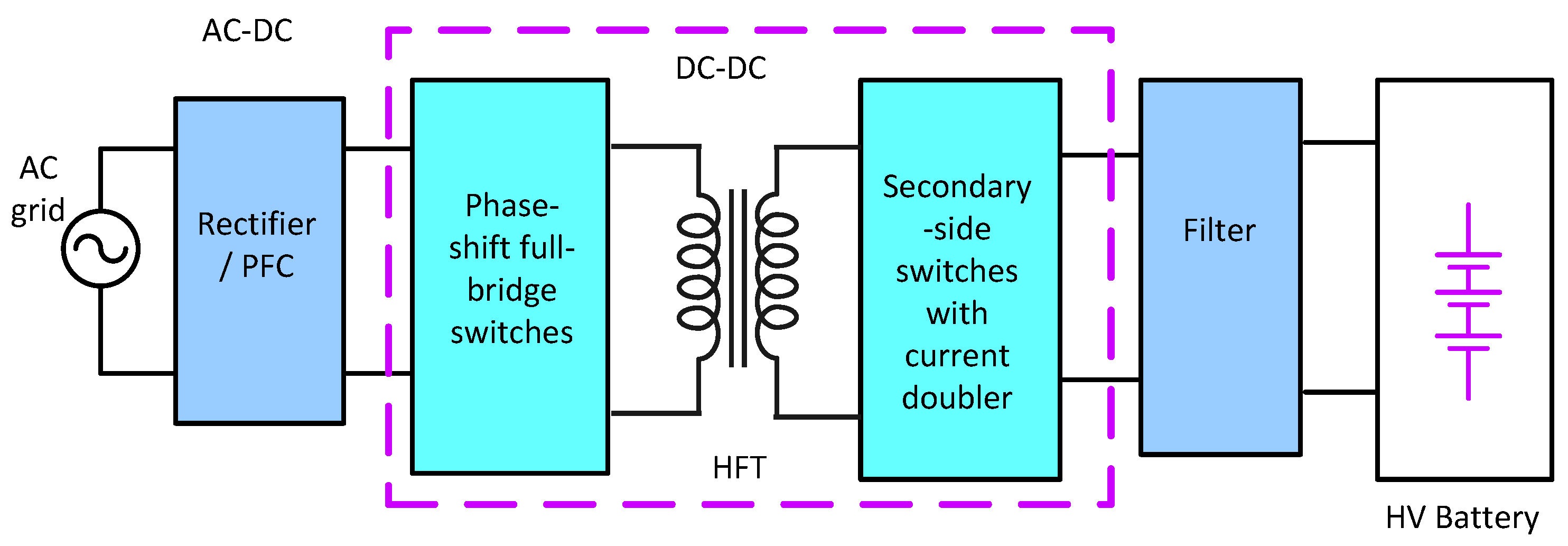
Many methodologies have been proposed for treating the issues of the OBC chargers [19,22,23]. However, they suffer from some disadvantages such as complex configurations and/or complex control schemes, high-cost solutions, narrow load regulation characteristics, and limited efficiency improvement. The block diagram of the conventional OBC charger systems is shown in Figure 1. The structure is composed of two stages; the first is the rectifier (AC–DC) or power factor correction (PFC) circuit, and the second is the high-frequency link DC–DC converter charger, including high-frequency (HF) transformer isolation. A filter can be an option for DC current smoothing for a high voltage battery pack. However, utilizing HF transformers for galvanic isolation and a wide range of output voltage has a negative effect on power density and efficiency characteristics [14,15,16,17,18]. Normally, the total efficiency is about 94% because of the multi-stage structure configuration. However, it is difficult to improve the overall efficiency in the multi-stage structure.
Various soft-switching high-frequency-linked DC–DC converters have been introduced for on-board EV battery chargers [24,25,26]. Phase-shift modulation (PSM) full-bridge (FB) DC–DC converters have been widely utilized in several works [24]. Zero-voltage soft-switching (ZVS) of semiconductor devices is achieved with constant switching frequency operation [25]. However, these full-bridge phase-shift converters have several drawbacks, such as high circulating current and narrow ZVS range. Due to the extended range of chargers’ power regulation, the lagging-leg switches cannot realize ZVS soft-switching at light-load operation conditions [26]. Continuous improvements have been developed in order to prolong the ZVS soft-switching range [27,28,29,30]. One method to extend the soft-switching range is by using additional passive auxiliary circuits to the conventional phase-shifted power converter. However, the primary current continues circulation through the primary circuit during the freewheeling intervals causing extreme conduction losses. Additional active switch circuits or extra HF transformers are utilized for the reduction of the circulation current [31,32]. However, these additional components increase the total cost. Moreover, secondary-side diodes are subjected to high voltage spikes and oscillations during turning-off. Thus, the reverse recovery of rectifying diodes in secondary-side causes oscillations and high-voltage overshoots because the EV battery pack voltage is usually high [32,33,34,35,36,37,38,39,40,41,42].
This paper introduces the analyses and performance of a phase-shift converter investigated and designed to operate at 40 kHz and 3.2 kW for EV on-board chargers. The proposed design enables high-frequency switching without sacrificing conversion efficiency. One of the major challenges in high-frequency power converter design is to reduce the parasitic components of printed circuit boards (PCBs), which can cause a faulty triggering of switches leading to circuit failure [43,44,45]. Another challenge is the efficient design of magnetic components, which requires minimizing the impacts of skin and proximity effects on the transformer winding to reduce the conduction loss at high frequencies. The leakage inductance of the high-frequency (HF) transformer is modeled and designed for the proposed converter. A comprehensive system-level power loss analysis is completed and confirmed with the help of experimental results. The prototype circuit can achieve an approximate efficiency of 96% with an appropriate design of the driving circuit and control signal.
2. Proposed Topology
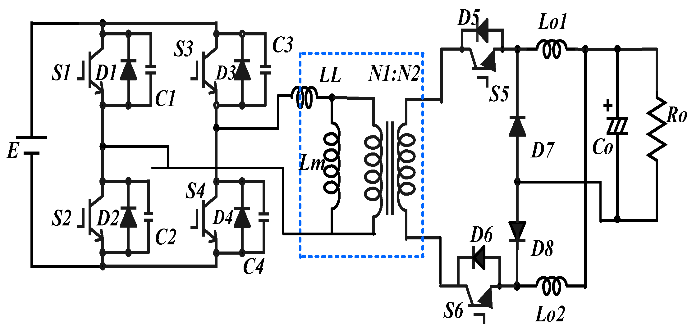
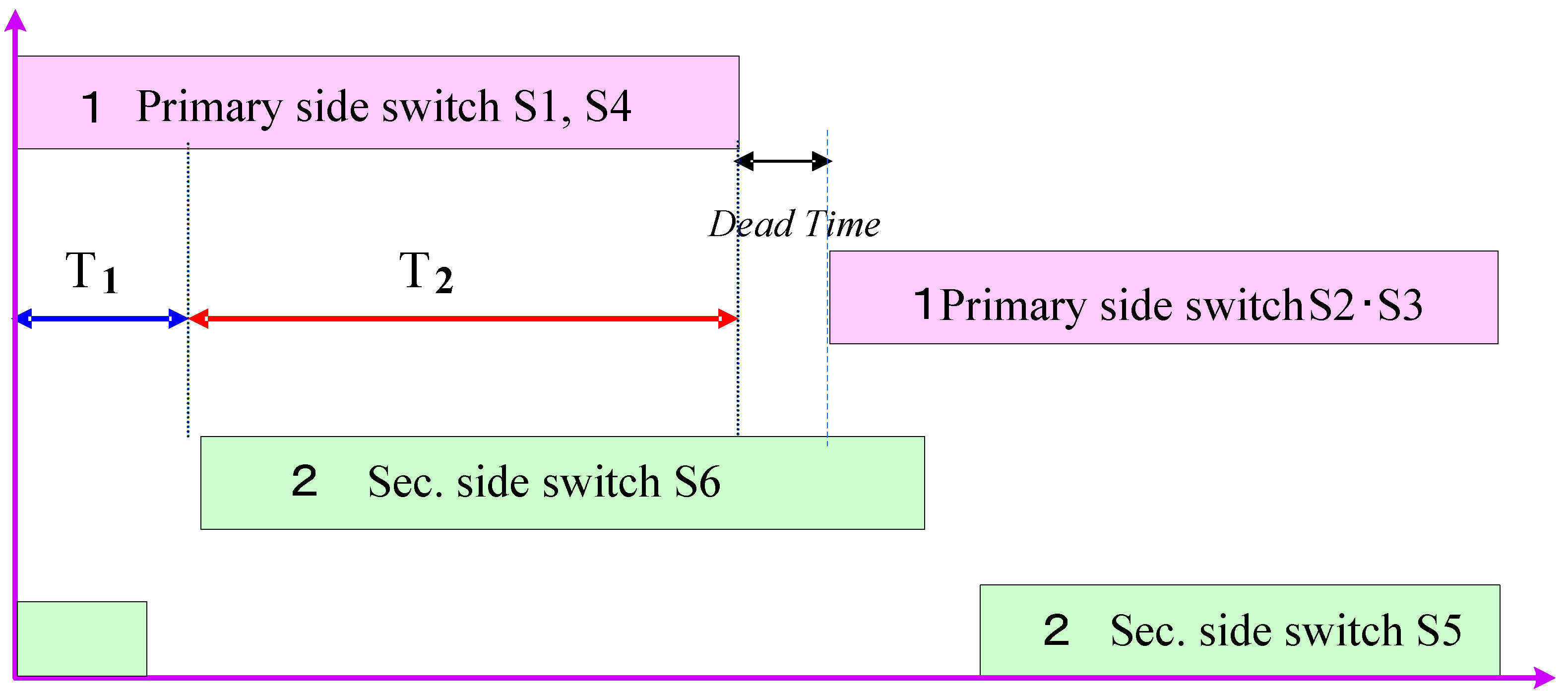
The proposed circuit consists of a full-bridge phase-shift topology. It is considered the most promised topology at high power levels, where the use of four switches is justifiable. The secondary circuit of the high-frequency transformer consists of two controlled switches for synchronous rectification, as shown in Figure 2. The current doubler works as the same principle as a full-wave rectifier. This configuration will reduce the copper loss in the transformer secondary as 50%, as stated in [31]. Converters with current doubler rectifiers have a smaller volume of magnetic components. The gate pulse signal applied for active switches is shown in Figure 3. The duty factor (or cycle) can be defined as the ratio of the on-time of switches S1, S4 overlapped with S6 to the total on-time of S1 and S4:
where T1 is the ON period of switch S6 that overlaps with the on-time of S1 and S4. The total on-time of switches S1 and S4 is equal to T1 + T2.
3. Operation Principle
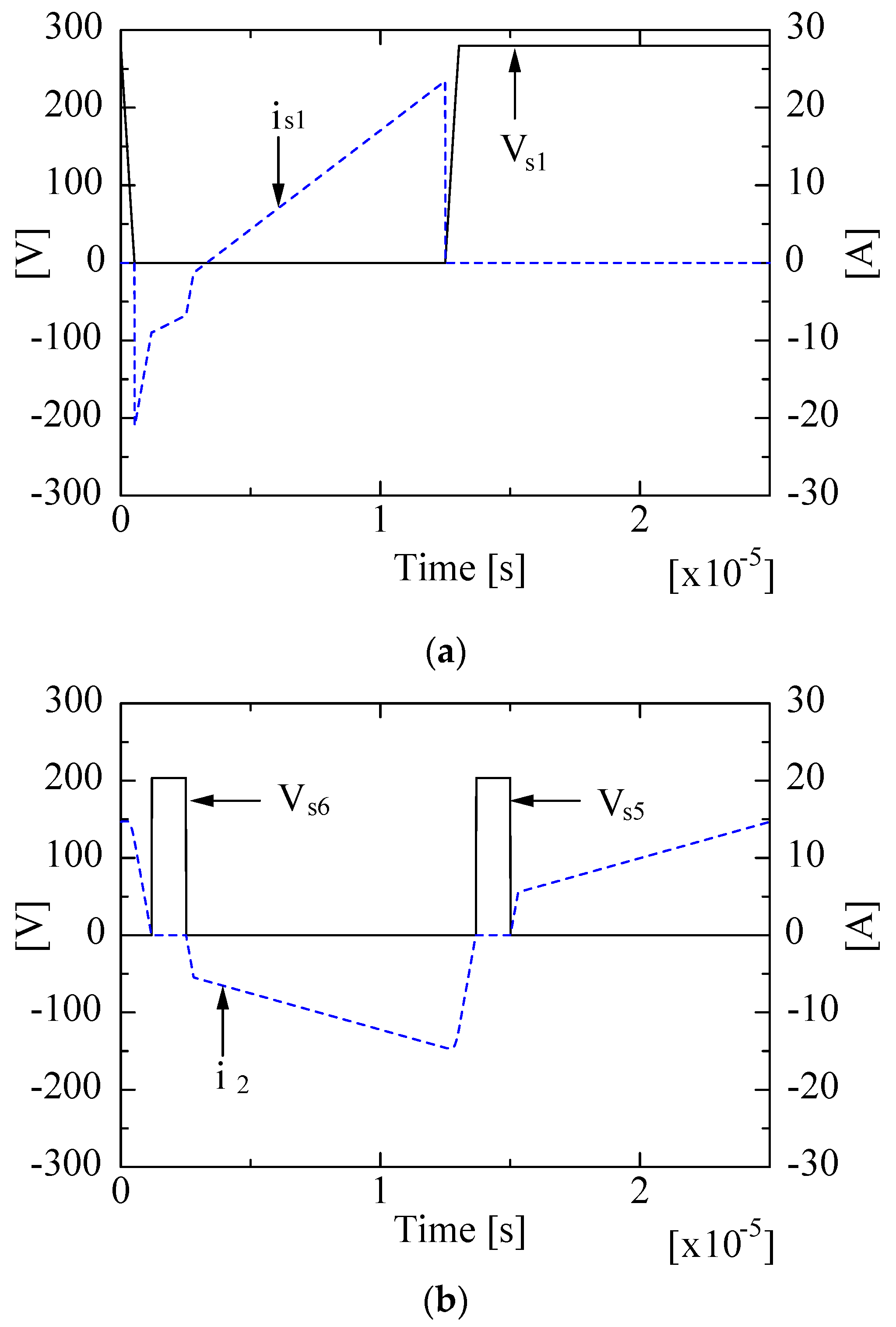
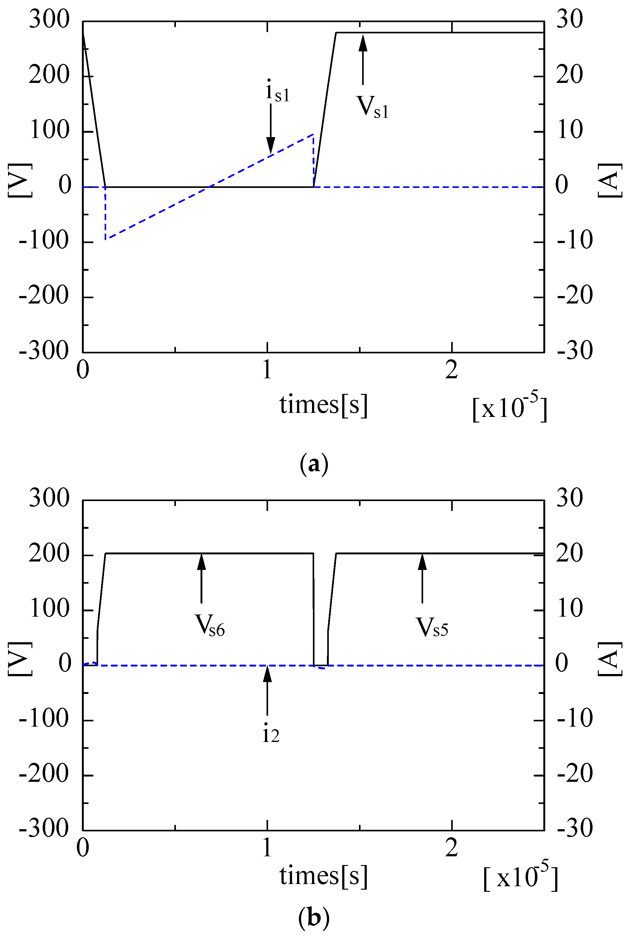
The simulation results are shown in Figure 4 and Figure 5. The primary switches voltage and the related current are shown in Figure 4a. The voltage and current of switches in secondary-side controlled by phase-shift are shown in Figure 4b. The primary current (ip) can increase or decrease during the dead time period. This implies that the stored energy in the leakage inductance Llk discharges in order to achieve ZVS soft-switching. The simulation results of the proposed on-board charger controlled by the phase-shifting technique are shown in Figure 5a,b. The developed charger circuit is working in normal operation. In this mode, the circuit is supplying the energy from the grid to the propulsion battery.
4. Operation Analysis
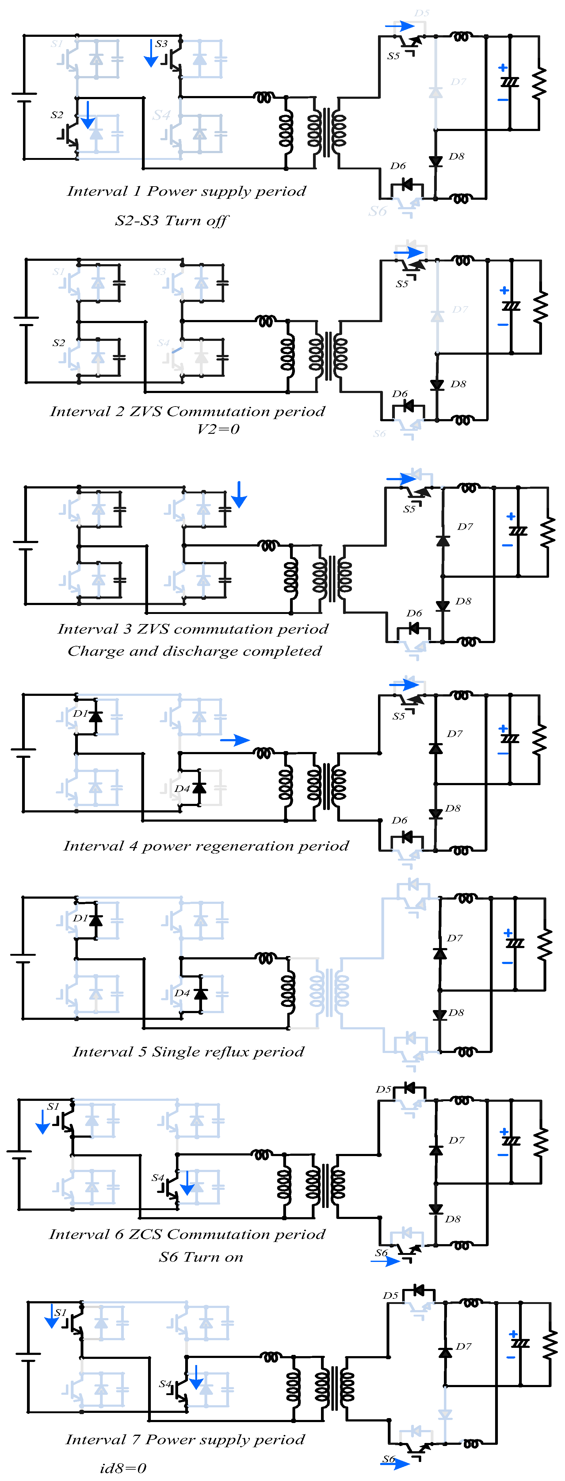
In order to investigate the operation of the studied converter, one assumption is considered. The switching devices are assumed to be ideal isolated gate bipolar transistors (IGBTs), excluding the parasitic capacitors and the reverse conducting diodes. All IGBTs have the same parasitic capacitances. The rectifying diodes are assumed ideal, and the output filter inductor LO is massive enough to be treated as a constant current (CC) source during periods of switching. The output voltage is regulated in the conventional phase-shift manner using the driving signals depicted in Figure 3. As depicted in Figure 6, there are seven operating intervals in one switching cycle t0–t7 (from Interval 1 to Interval 7. The operation principle of one cycle is described, and the equivalent circuits of each operating interval are shown in Figure 6.
Interval 1 (t0–t1): Interval 1 starts when the primary-side switches S2 and S3 begin conduction state. The primary current ip(t) in the proposed charger increases linearly and can be expressed as
where n = N1/N2 for the turns ratio of the HF transformer.
The power transfers from primary to the secondary circuit through the HF transformer. For this reason, this interval is called the power supply period. At this interval, the battery charging current is flowing through switch S5, capacitors Co, output inductors LO1–LO2, and diodes D6 and D8. From this power flow path, one can realize soft-switching power transfer to the required output side. The rectified output voltage Vrec(t) equals the sum of the voltage across the current doubler inductor VLO1 and the output voltage of VO. The secondary voltage is expressed as:
Then, the HF transformer primary voltage of a high-frequency transformer (HFT) can be expressed as:
This interval finishes when the active switches S2 and S3 are turned OFF with ZVS soft-switching.
Interval 2 (t1–t2): Interval 2 starts when switches S2 and S3 are turned OFF with ZVS commutation at t1. For this reason, this period is called the ZVS commutation period. Capacitors C1 = C2 = C3 = C4 = C start charging. Vp(t) decreases linearly and at a fast rate. The duration of this interval is a very short time interval.
The voltage across switches and capacitors is expressed as:
Interval 3 (t2–t3): Interval 3 starts when diode D7 conducts. At the moment t2, the voltage across S2 is equal zero, and thus, the switch S2 is turned ON succeeding ZVS soft-switching. This period is called.
ZVS—charge and discharge completed. The primary voltage Vp(t) equals the same magnitude as in both Intervals 1 or 2, and it is applied to the transformer leakage inductance Llk in the primary-side of HFT. However, current ip(t) in primary-side starts to decrease with a linear slope calculated by the following equation:
The currents through diode D6 also decrease with a linear inclination described by:
Interval 4 (t3–t4): Diodes D1 and D4 conduct at the beginning of this interval. Current in the secondary side is decreasing in switch S5 and diode D6. Then, the voltage is applied to Llk, and ip(t) decreases linearly. At time t4, the switch S5 and diode D6 are turned OFF under zero-current soft-switching (ZCS). This period is called the power regeneration period.
Interval 5 (t4–t5): In this interval, S5 and D6 commutates. This interval current circulates in the primary and secondary circuits. No power transfer from the primary to the secondary side. Then, energy stored in the output inductance and capacitance in the onboard charger still supplies energy for charging the EV battery, as shown in Figure 6. The accumulated energy in the leakage inductance is returning back to the source. However, in the conventional phase-shift full-bridge converter, freewheeling intervals exist when Vp(t) is zero. Thus, the circulating current circulates during these intervals in the primary circuit of the HF transformer. The current is considered as a significant disadvantage of the conventional phase-shift converters used for EV battery charging applications. That is because the current continually exists for a wider range of charging voltage like battery charger applications. However, the conduction power losses consumed in the primary circuit of the HF transformer is considerably enlarged due to the primary current [7]. Particularly, the conduction losses produced by the primary-side current are maximum when the EV battery voltage is nearby the minimum level. This is due to the long period of freewheeling phases in this condition. Furthermore, the primary-side current ip(t) in the proposed circuit is reorganized to zero when primary voltage Vp(t) tends to zero, and no current flows in the primary-side. In other words, the problem of circulating current is eliminated. Consequently, the conduction power losses consumed in the primary circuit of HF transformers could be significantly reduced during the EV battery charging procedure. This period is called the single reflux period.
Interval 6 (t5–t6): Interval 6. Gating signals are applied to switches S1, S4, and S6. These switches are turning on with ZCS due to HF transformer leakage inductance Llk. For this reason, this period is called the ZCS commutation period. The current in the primary side ip(t) flows through Q1-HFT-Q4 in this interval. The current in the primary is increasing linearly and can be calculated as:
Moreover, the lower-side switch S6 and upper-side diode D5 in the secondary circuit start conduction. The charging current flows directly to the battery through only switch S5 and diode D6. At the end of this interval, the diode D8 is turned OFF.
Interval 7 (t6–t7): Interval 7 begins when lower-side diode D8 is turned OFF. However, the charging energy is supplied from charger output to the EV battery as ever. This period is called the power supply period. The charging energy passes through S6 and D5 in the secondary circuit of HFT. However, the current in the primary circuit can be expressed in this interval as:
where is(t) is the secondary current and n is the turns ratio of HFT.
5. Feedback Control Loop
Arduino Mega2560 is used for controlling the proposed DC–DC converter circuit. As the control system is based on a microcontroller, all the parameters can be adjusted through changes in the firmware. The basic control loop uses a simple proportional integral (PI) controller operation. The control board generates the driving pulses for the switches using an Arduino controller and the closed-loop control of the output voltage in the DC–DC converter. The output power of the DC–DC converter is regulated according to the voltage and current given to the load. The current is measured on the high side by a simple circuit using the INA138-Q1. The INA138-Q1 delivers output current proportional to the sensed load current. The device common-mode voltage is 40 V, but it can be much higher by floating the ground pin and buffering its output current with a high voltage PNP transistor. Voltage is measured by a voltage divider and buffered using the TLC2272A-Q1 that has low offset voltage and 2.2 MHz of unity-gain bandwidth. Both current and voltage are converted from analog to digital by using an analog to digital converter. In a charging system, load measurement is key for charging optimization with high accuracy. Low side measurements can provide accuracy but are not capable of detecting short to ground. High side measurements can achieve accuracy and can detect short to the ground; however, the high common-mode voltage, up to 400 V, puts constraints on the design. With a few additional components around the current shunt, 400 V common-mode voltage can be achieved with both accuracy and short to ground features. Measuring the 400 V battery voltage requires a high impedance resistive voltage divider and a low output impedance buffer for conditioning the signal. The voltage divider ratio is on the order of 0.01 if the electronics circuit supply voltage is 5 V. To maintain the desired accuracy, low offset, low input capacitance, and high impedance op-amp are required. Two op-amps or a two-channel op-amp is needed to satisfy the current and voltage measurement requirements.
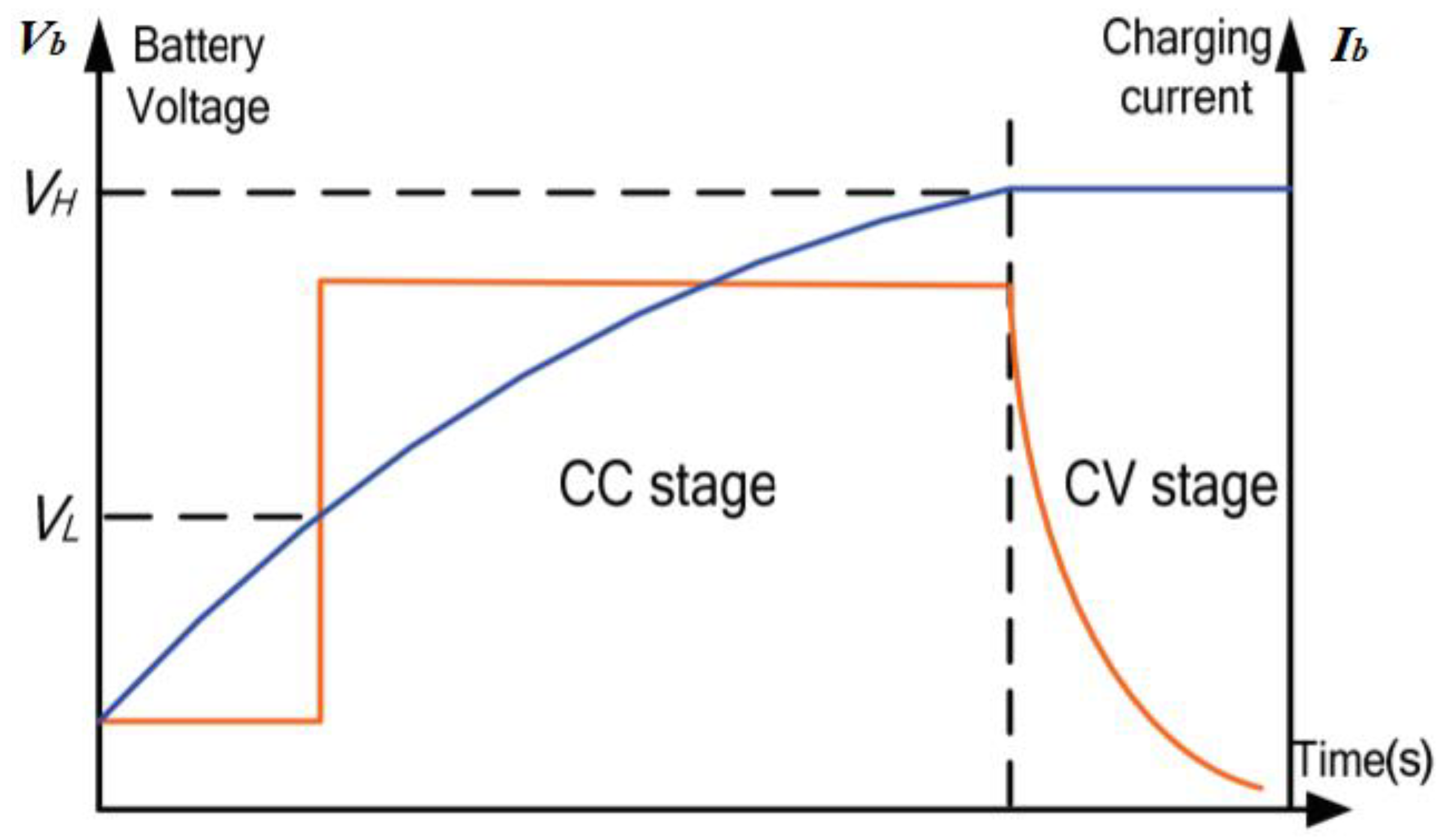
The charging strategy is consisting of two stages; the first is the constant current CC stage; the second is the constant voltag (CV) stage. As presented in Figure 7, the charging current Ib decay as the voltage Vb of the battery increases. Firstly, the EV battery is charged at a constant charging current until the EV battery voltage equals the predetermined upper-limit voltage VH. Then, current decays exponentially with a constant voltage charging until the current reaches a predefined minimum-limit current.
By using the CC–CV charging strategy, the battery is charged by a degrading current after changing from the CC stage to the CV stage, avoiding overcharging the battery. The charging control strategy is applied in the control of the onboard charger power converter. The selection mode realizes the CC–CV charging strategy, as illustrated in Figure 7. The charging mode selected signal is determined according to the existing operating conditions (the measured voltage uf(k), the measured currents if(k), and the previous charging mode).
6. Experimental Setup
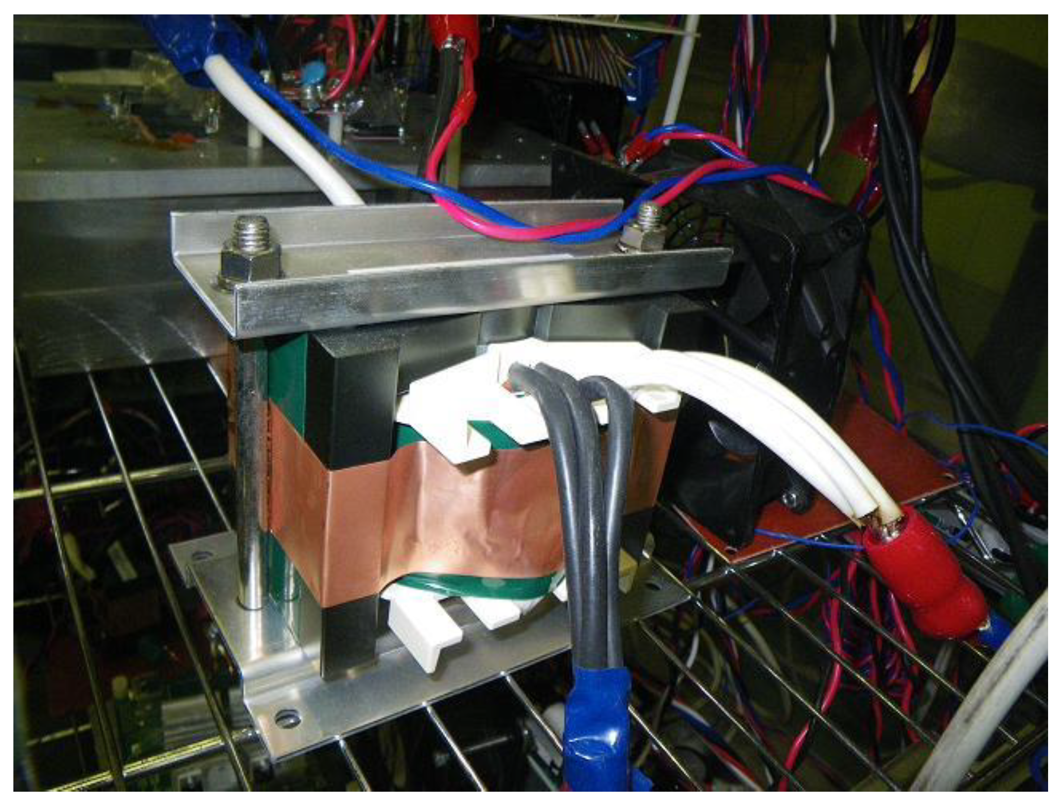
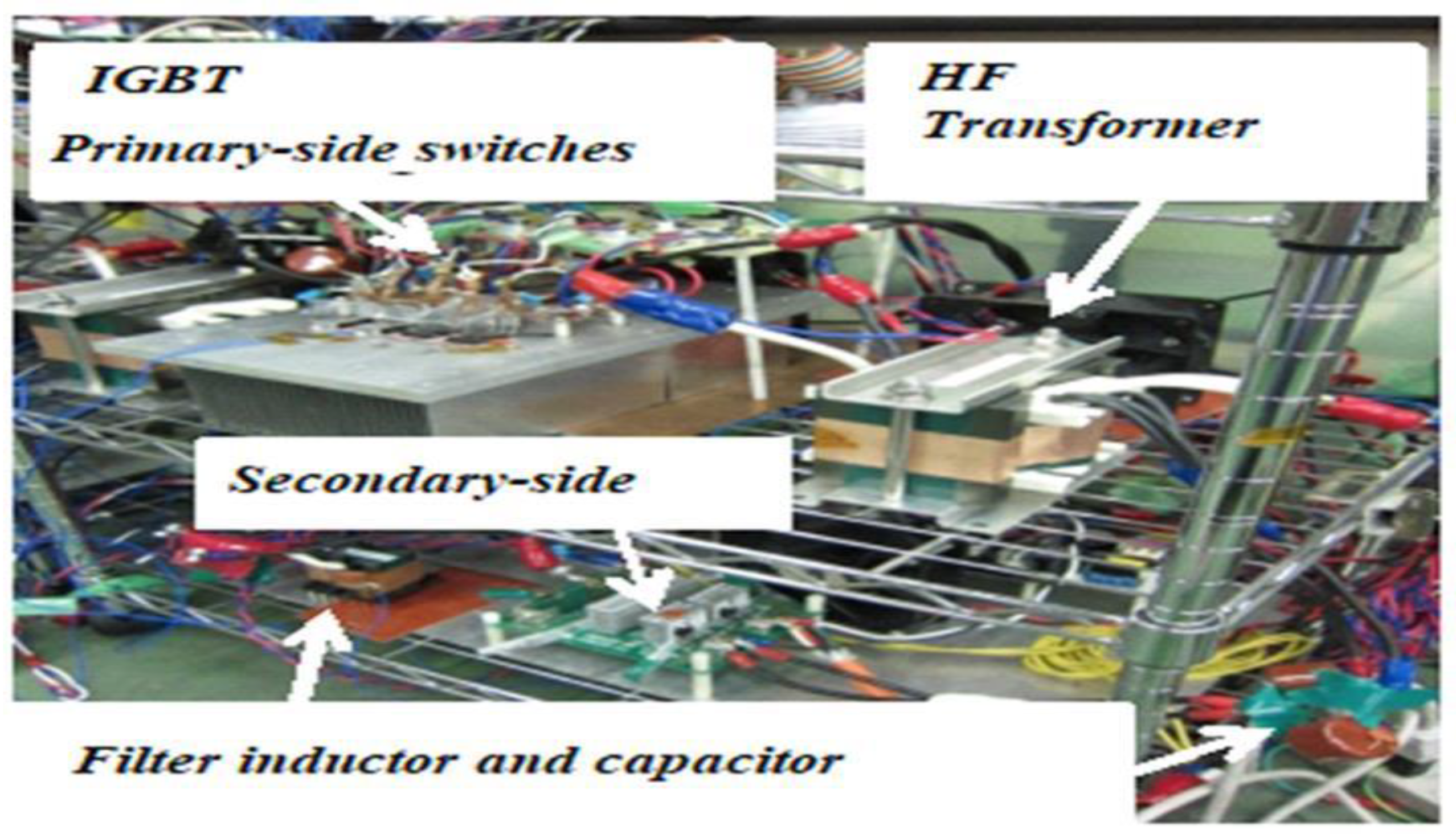
An experimental setup of a 3.2 kW battery charger prototype is implemented. The high-voltage (HV) nickel–metal hydride (NiMH) battery is substituted as an electronic load prepared in the laboratory. The AC source is given by an AC power supply in the early stage of the experimental setup. The used high-frequency transformer with a ferrite core (Ferrite PQ107) installed in the DC–DC converter is shown in Figure 8. The semiconductor devices in the charger circuit by using IGBTs with 600 V rated voltage in the charger circuit (SKM150GB128D Vces = 600 V, Ic = 150 A (25 °C)). The power losses are calculated under the condition of the rated output power. Figure 9 shows the appearance of the implemented phase-shift full-bridge DC–DC converter with current doubler in secondary-side suitable for OBC charger systems.
To verify the effectiveness of the proposed charger, an experimental setup was carried out using prototype circuit components. The circuit parameters and system specifications are listed in Table 1. A prototype circuit has been built for the proposed converter with a rated power of 3.2 kW with the components in Table 1. The prototype was tested by applying the constant current and constant voltage (CC–CV) charging control technique. The circuit design has an input voltage range Vs = 280 to 400 V; the output voltage VO ranges from 250–420 V. The charging current according to the Constant Current (CC) mode Ib is about 7.8 A at a switching frequency fs of about 40 kHz.
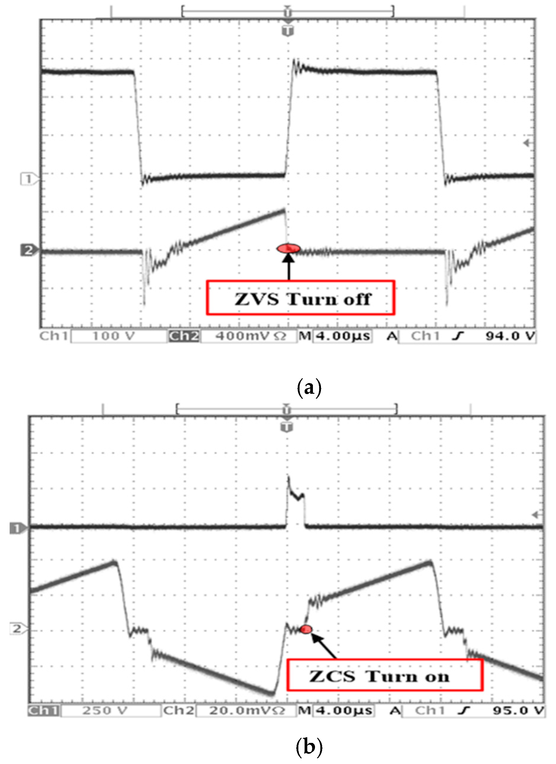
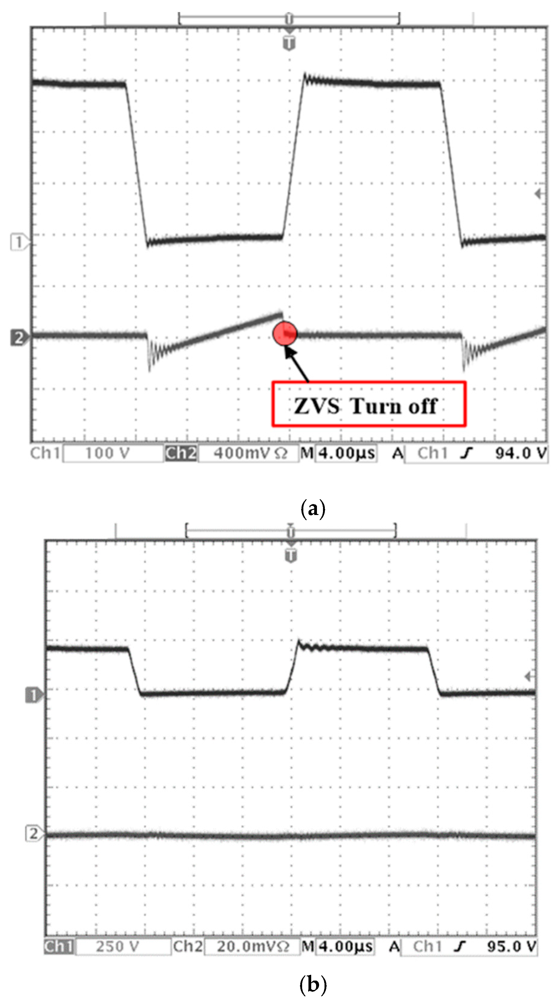
The proposed charger was designed to achieve soft-switching conditions. These conditions ensure ZVS turn-on from no-load to full loading and to diminish the circulating current produced in the primary-side. In this design, the proposed on-board charger is controlled using a pulse width modulation (PWM) technique with a constant frequency. Two control loops are used for the implementation of the EV battery charging controller. The first is the current inner control loop, and the second is the voltage outer control loop. This control scheme is based on the CC–CV charging algorithm: two PI-type controllers are used to adjust the charging current and EV battery voltage. Thus, the appropriate duty cycle is produced for charging the EV battery. Figure 10 shows the ZVS waveforms in the lagging-leg in the case of a 0.9 duty cycle (in secondary switches) during the normal EV charging process. The waveforms of primary-side switches after changing the duty cycle to 0 in the secondary side are shown in Figure 11. From these two figures, the lagging-leg switches in the studied charger circuit are fruitfully turned ON, achieving ZVS in different loading conditions.
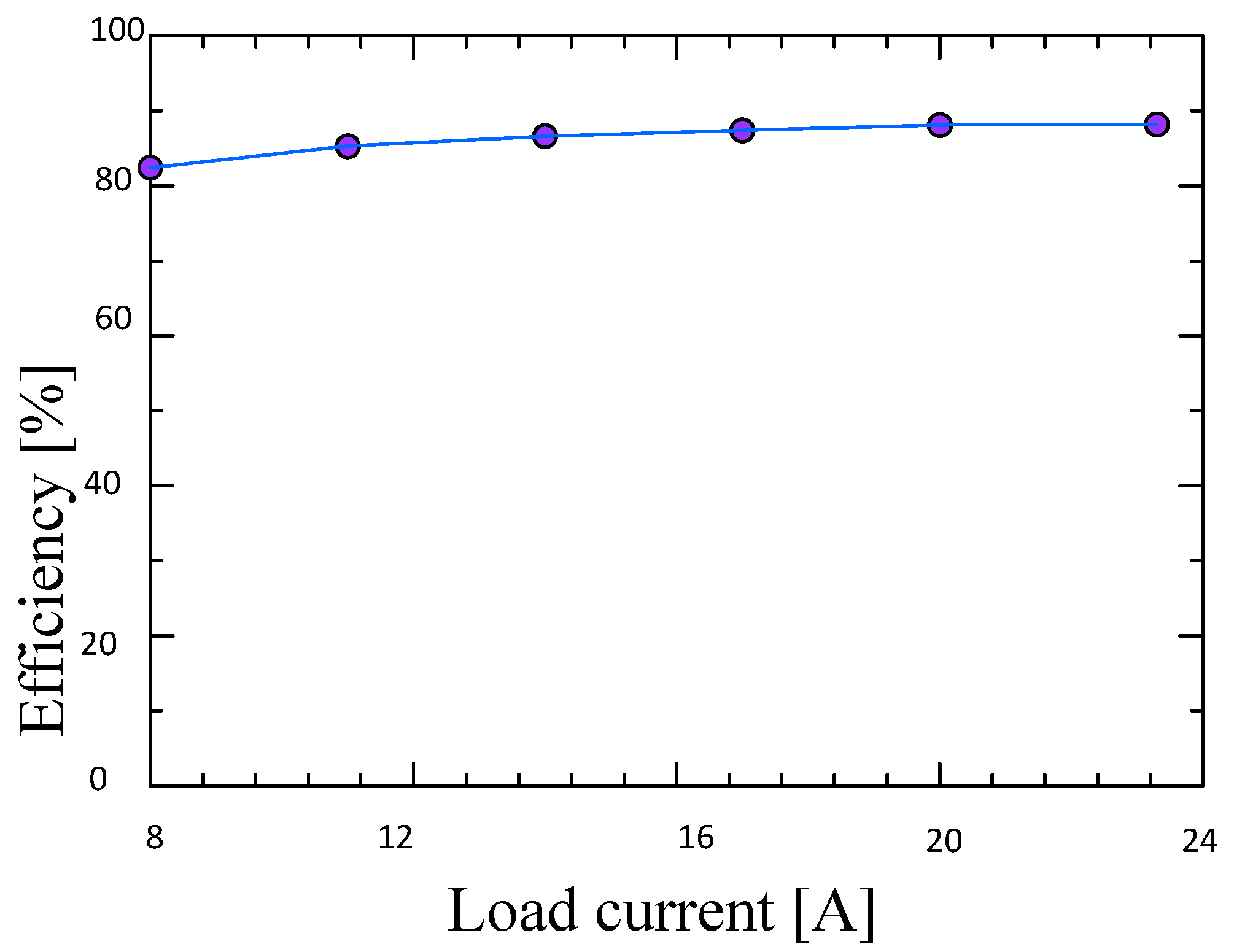
The primary switch current and voltage measured waveforms are shown in Figure 10. As one can notice from Figure 11a, all active power switches in both full-bridge-arms can realize soft-switching operation. In this situation, the inner upper-side and outer lower-side switches S1 and S4 can achieve a ZVS soft-switching operation. Figure 12 illustrates the output current versus efficiency characteristics of current doubler secondary with semiconductor devices rated 600 V. Interpolation of experimental data is used in this figure when a theoretical model is unavailable. We Interpolate between two measurements and observations to save money and time. The simplest interpolation method is to locate the nearest data value, and assign the same value. One of the simplest methods is linear interpolation. Linear interpolation is quick and easy, but it is not very precise.
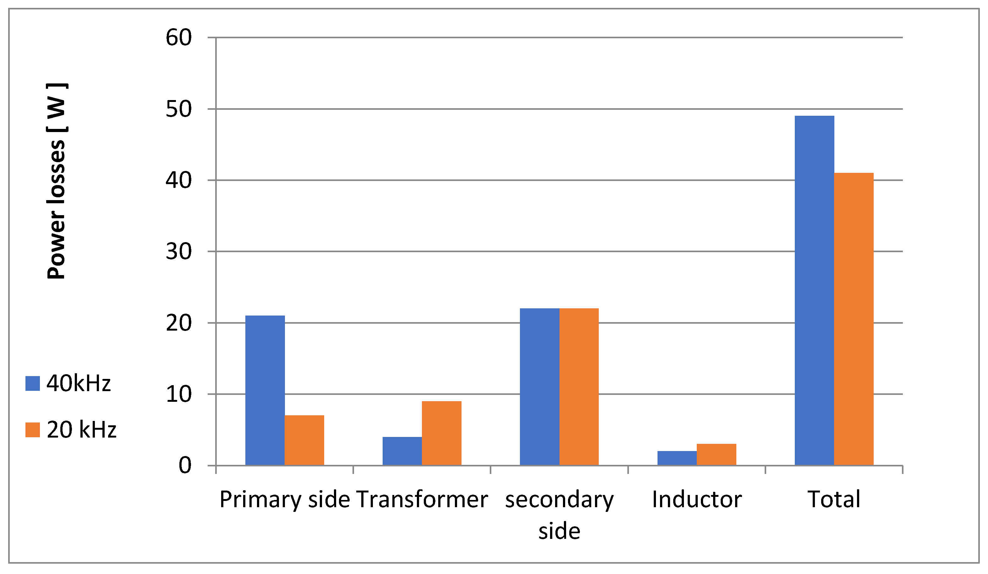
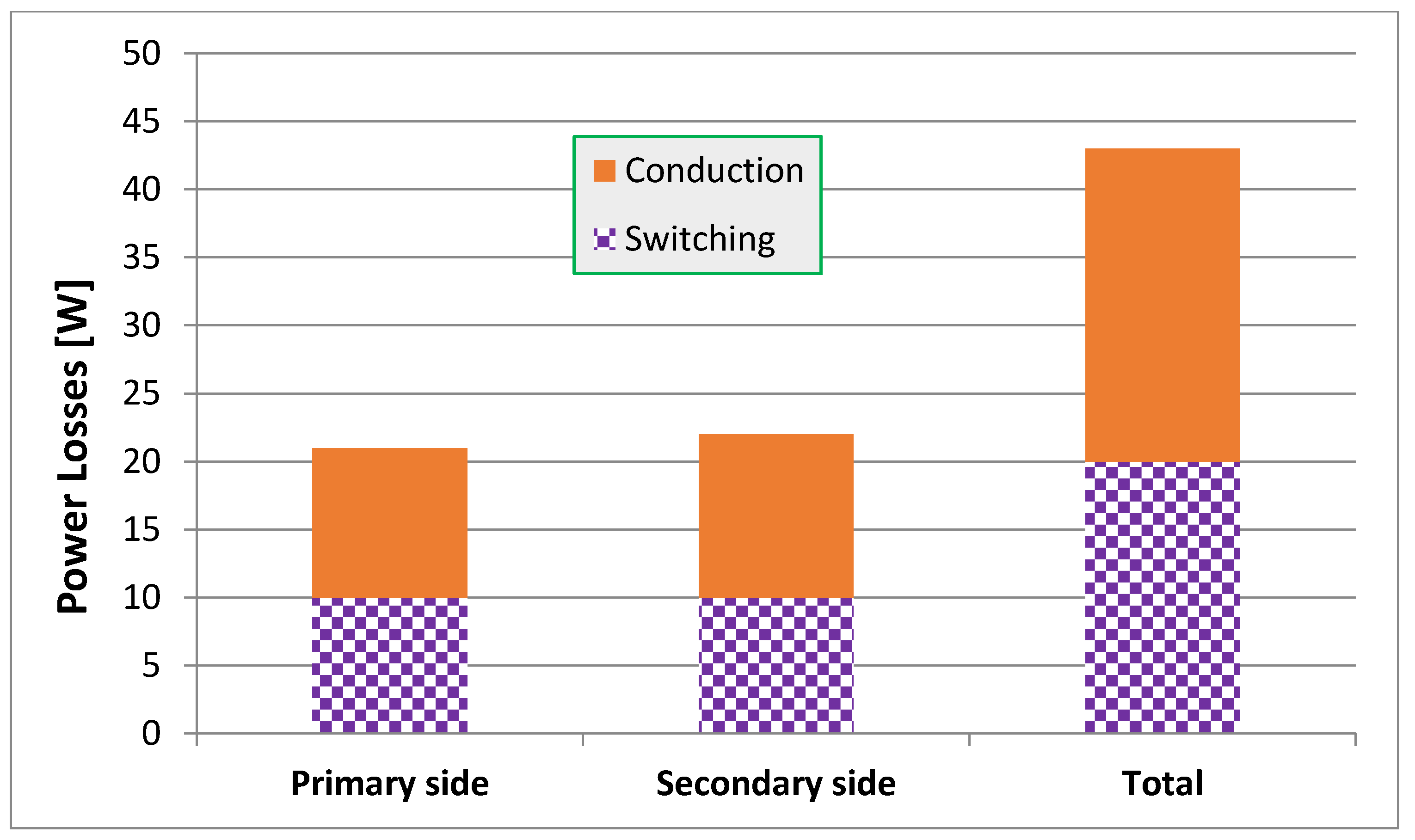
Figure 13 depicts the quantitative power loss analysis for active switches in the proposed charger circuit by using IGBTs with 600 V rated voltage in the proposed circuit topology. The loss constituents can be categorized into primary-side power switches, HF transformers, and secondary-side rectifier switches and an inductor filter as the loss components. The power losses are calculated at the rated output power condition of 3 kW. One can realize that the overall consumed power losses of the whole circuit are 49.5 W in the case of 40 kHz switching frequency. Figure 14 describes the evaluation of loss components under typical operation. The loss constituents can be categorized into conduction losses and switching losses. The primary-side losses are due to primary-side IGBTs. The secondary-side losses are due to IGBTs and current doubler diodes. The switching losses are calculated in the case of 40 kHz switching frequency. The total switching losses are 20 W and the total conduction losses are 23 W. However, the conduction losses are 15% higher than switching losses due to soft-switching operation.
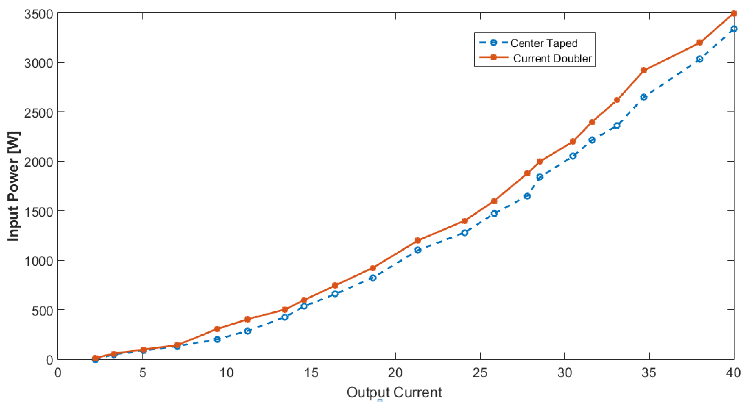
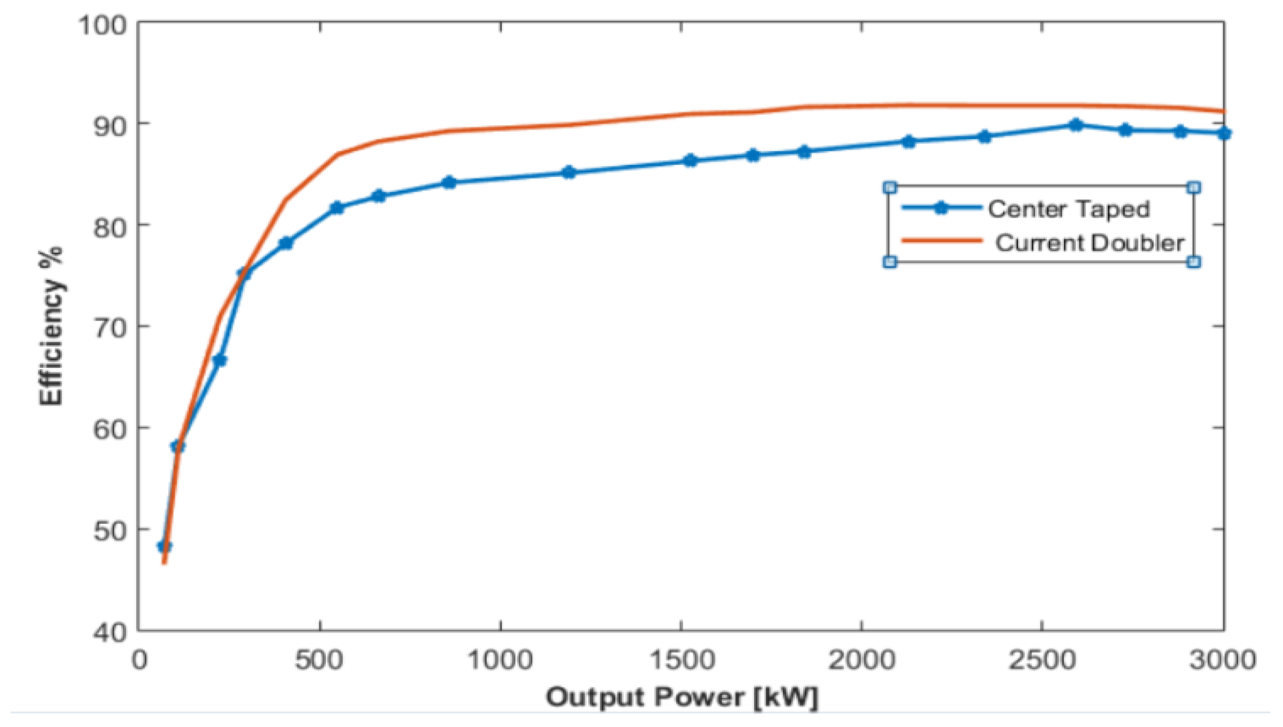
Figure 15 illustrates the charger output power characteristics comparing the current doubler (CD) topology with the center-taped (CT) secondary-side circuit. From this figure, the proposed power converter circuit can deliver its output current, achieving soft-switching operation. In the case of rated power settings, the proposed power converter can achieve a measured efficiency of about 92%. Figure 16 depicts the measured charger efficiency during the EV battery charging period. As appears in Figure 16, the studied on-board charger achieves a better performance as compared with the conventional hard switching charger. This is owing to the wider ZVS soft-switching range, reduced circulation current, ZCS operation for all the active switches, and lower turns ratio. The implemented charger has a maximum efficiency of about 96% at rated-load charging conditions during one cycle of the CC–CV charging scheme. Figure 15 shows the efficiency characteristics of the converter with a secondary-side current doubler as compared with the center-tapped DC–DC converter. In this case, the active power switches are rated 600 V. Noticing this figure, the measured efficiency of the studied charger is higher than that of the previously developed charger with the center-tapped circuit in the secondary-side [12] and two-level circuit with the current doubler DC–DC converters in a wide range of charging current ratings.
The studied soft-switching DC–DC converter circuit has many advantages and can be summarized in the following:
- (1)
- All the active switches can achieve full-ZVS range without duty cycle loss;
- (2)
- All the rectifying diodes can operate at ZCS turn-off;
- (3)
- Circulating current is minimized;
- (4)
- The output filter inductor is small sized;
- (5)
- Improved HF transformer utilization is achieved for applications of EV battery onboard charger;
- (6)
- The circuit has lower voltage stress on the secondary-side diodes.
Furthermore, the implemented DC–DC converter can achieve an efficiency of about 94% or more around the rated power settings. In this case, only one-diode drop exists in the charging current path. In addition, the transformer secondary winding is rated for one half the loads current, and no center-tapped connection is required. The two output filter inductors can be coupled or integrated on a single core.
7. Conclusions
A phase-shift PWM DC–DC converter with a current doubler rectifier was proposed using clarified circuit operation and features. The converter circuit is verified using the theory of operation, details of design, and various experimental results. Moreover, the overall circuit performance is discussed. Soft-switching operation was realized against load fluctuation by constant voltage control. From the simulation results, it was confirmed that soft-switching operation is possible in the entire output range during circuit operation. A further improvement in the proposed on-board charger efficiency can be realized by using the current doubler rectifier. The proposed charger attains superior transformer utilization and contains fewer circuit components. Moreover, the studied DC–DC converter has lower voltage stresses in the secondary-side components for EV onboard charging applications. Power loss analysis was discussed for all components of the studied DC–DC converter. The experimental results for a 3.2 kW prototype converter emphasize the merits of the suggested circuit for onboard charger application. The circuit achieves an overall efficiency of 92% during the charging process in the CC–CV control mode. The efficiency of the current doubler circuit is higher than the center-tapped rectifier for the same operating conditions. The obtained results verify the suitability and effectiveness of the proposed circuit topology for the on-board EV battery charger applications.
Author Contributions
Conceptualization, K.S.; methodology, K.S.; software, Z.M.A.; validation, K.S., Z.M.A. and M.A.; formal analysis, K.S.; investigation, Z.M.A.; resources, K.S.; data curation, M.A.; writing—original draft preparation, K.S.; writing—review and editing, M.A.; visualization, Z.M.A.; supervision, K.S.; project administration, Z.M.A.; funding acquisition, M.A. All authors have read and agreed to the published version of the manuscript.
Funding
This research received no external funding.
Conflicts of Interest
The authors declare no conflict of interest.
Nomenclature
| AC | alternating current |
| AC–DC | alternating current–direct current rectifier |
| CD | current doubler topology |
| CT | center-taped |
| CC | constant current charging |
| CV | constant voltage charging |
| CC–CV | constant current–constant voltage charging |
| DC | direct current |
| DC–DC | direct current–direct current converter |
| EV | electric vehicle |
| FB | full-bridge |
| HFT | high-frequency transformer |
| HV | high voltage |
| IGBTs | isolated gate bipolar transistor |
| LLC | inductor–inductor–capacitor |
| NiMH | nickel–metal hydride battery |
| OBC | on-board battery charger |
| PCBs | printed circuit boards |
| PEVs | plug-in electric vehicles |
| PFC | power factor correction circuit |
| PHEVs | plug-in hybrid EVs |
| PI | proportional integral controller |
| PSM | phase-shift modulation |
| PWM | pulse width modulation |
| SRC | series resonance converters |
| ZVS | zero-voltage soft-switching |
| ZCS | zero-current soft-switching |
References
- Saber, A.Y.; Venayagamoorthy, G.K. Plug-in Vehicles and Renewable Energy Sources for Cost and Emission Reductions. IEEE Trans. Ind. Electron. 2010, 58, 1229–1238. [Google Scholar] [CrossRef]
- Lee, B.K.; Kim, J.P.; Kim, S.G.; Lee, J.Y. A PWM SRT DC/DC Converter for 6.6-kW EV Onboard Charger. IEEE Trans. Ind. Electron. 2016, 63, 894–902. [Google Scholar] [CrossRef]
- Kim, S.; Kang, F.-S. Multi-functional On-board Battery Charger for Plug-in Electric Vehicles. IEEE Trans. Ind. Electron. 2014, 62, 1. [Google Scholar] [CrossRef]
- Yilmaz, M.; Krein, P.T. Review of Battery Charger Topologies, Charging Power Levels, and Infrastructure for Plug-In Electric and Hybrid Vehicles. IEEE Trans. Power Electron. 2013, 28, 2151–2169. [Google Scholar] [CrossRef]
- Haghbin, S.; Lundmark, S.; Alakula, M.; Carlson, O. Grid-Connected Integrated Battery Chargers in Vehicle Applications: Review and New Solution. IEEE Trans. Ind. Electron. 2012, 60, 459–473. [Google Scholar] [CrossRef]
- Sakr, N.; Sadarnac, D.; Gascher, A. A review of on-board integrated chargers for electric vehicles. In Proceedings of the 2014 16th European Conference on Power Electronics and Applications, Lappeenranta, Finland, 26–28 August 2014; pp. 1–10. [Google Scholar]
- Subotic, I.; Levi, E.; Ivan, S. A review of single-phase on-board integrated battery charging topologies for electric vehicles. In Proceedings of the 2015 IEEE Workshop on Electrical Machines Design, Control and Diagnosis (WEMDCD), Torino, Italy, 26–27 March 2015; pp. 136–145. [Google Scholar]
- Shi, C.; Tang, Y.; Khaligh, A. A Three-Phase Integrated Onboard Charger for Plug-In Electric Vehicles. IEEE Trans. Power Electron. 2018, 33, 4716–4725. [Google Scholar] [CrossRef]
- Rippel, W.E. Integrated Traction Inverter and Battery Charger Apparatus. U.S. Patent 4,920,475, 24 April 1990. [Google Scholar]
- Pellegrino, G.; Armando, E.; Guglielmi, P. An integral battery charger with power factor correction for electric scooter. IEEE Trans. Power Electron. 2010, 25, 751–759. [Google Scholar] [CrossRef] [Green Version]
- Lee, Y.-J.; Khaligh, A.; Emadi, A. Advanced Integrated Bidirectional AC/DC and DC/DC Converter for Plug-In Hybrid Electric Vehicles. IEEE Trans. Veh. Technol. 2009, 58, 3970–3980. [Google Scholar] [CrossRef]
- Sayed, K. ZVS Soft-Switched DC-DC Converter based Charger for Low Voltage battery in Hybrid Electric Vehicles. IET Power Electron. 2019, 12, 3389–3396. [Google Scholar] [CrossRef]
- Chang, H.-C.; Liaw, C.-M. An Integrated Driving/Charging Switched Reluctance Motor Drive Using Three-Phase Power Module. IEEE Trans. Ind. Electron. 2010, 58, 1763–1775. [Google Scholar] [CrossRef]
- Kim, J.-S.; Choe, G.-Y.; Jung, H.-M.; Lee, B.-K.; Cho, Y.-J.; Han, K.-B. Design and implementation of a high-efficiency on- board battery charger for electric vehicles with frequency control strategy. In Proceedings of the 2010 IEEE Vehicle Power and Propulsion Conference, Lille, France, 1–3 September 2010; pp. 1–6. [Google Scholar]
- Chuang, Y.-C.; Ke, Y.-L.; Chuang, H.-S.; Chen, H.-K. Implementation and analysis of an improved series-loaded resonant dc-dc converter operating above resonance for battery chargers. In Proceedings of the 2011 IEEE Industrial and Commercial Power Systems Technical Conference, Newport Beach, CA, USA, 1–5 May 2011; pp. 1–8. [Google Scholar]
- Emadi, A.; Rajashekara, K.; Williamson, S.; Lukic, S.M. Topological Overview of Hybrid Electric and Fuel Cell Vehicular Power System Architectures and Configurations. IEEE Trans. Veh. Technol. 2005, 54, 763–770. [Google Scholar] [CrossRef]
- Liu, C.; Gu, B.; Lai, J.-S.; Wang, M.; Ji, Y.; Cai, G.; Zhao, Z.; Chen, C.-L.; Zheng, C.; Sun, P. High-Efficiency Hybrid Full-Bridge–Half-Bridge Converter with Shared ZVS Lagging Leg and Dual Outputs in Series. IEEE Trans. Power Electron. 2012, 28, 849–861. [Google Scholar] [CrossRef]
- Oh, C.-Y.; Kim, D.-H.; Woo, D.-G.; Sung, W.-Y.; Kim, Y.-S.; Lee, B.-K. A High-Efficient Nonisolated Single-Stage On-Board Battery Charger for Electric Vehicles. IEEE Trans. Power Electron. 2013, 28, 5746–5757. [Google Scholar] [CrossRef]
- Lee, I.-O.; Moon, G.-W. Half-Bridge Integrated ZVS Full-Bridge Converter with Reduced Conduction Loss for Electric Vehicle Battery Chargers. IEEE Trans. Ind. Electron. 2013, 61, 3978–3988. [Google Scholar] [CrossRef]
- Beiranvand, R.; Rashidian, B.; Zolghadri, M.R.; Alavi, S.M.H. A Design Procedure for Optimizing the LLC Resonant Converter as a Wide Output Range Voltage Source. IEEE Trans. Power Electron. 2012, 27, 3749–3763. [Google Scholar] [CrossRef]
- Oh, C.-Y.; Kim, J.-S.; Kim, Y.-S.; Lee, B.-K. Design of resonant network based on power losses analysis of series resonant converter for on-board battery charger in EVs. In Proceedings of the 2012 IEEE Vehicle Power and Propulsion Conference, Seoul, Korea, 9–12 October 2012; pp. 1048–1053. [Google Scholar]
- Lo, Y.-K.; Lin, C.-Y.; Hsieh, M.-T.; Lin, C.-Y. Phase-Shifted Full-Bridge Series-Resonant DC-DC Converters for Wide Load Variations. IEEE Trans. Ind. Electron. 2010, 58, 2572–2575. [Google Scholar] [CrossRef]
- Whitaker, B.; Barkley, A.; Cole, Z.; Passmore, B.; Martin, D.; McNutt, T.R.; Lostetter, A.B.; Lee, J.S.; Shiozaki, K. A high-density, high-efficiency, isolated on-board vehicle battery charger utilizing silicon carbide power devices. IEEE Trans. Ind. Electron. 2014, 29, 2606–2617. [Google Scholar] [CrossRef]
- Choi, W.-Y.; Yang, M.-K.; Cho, H.-S. High-Frequency-Link Soft-Switching PWM DC–DC Converter for EV On-Board Battery Chargers. IEEE Trans. Power Electron. 2013, 29, 4136–4145. [Google Scholar] [CrossRef]
- Gautam, D.S.; Musavi, F.; Edington, M.; Eberle, W.; Dunford, W.G. An automotive onboard 3.3-kW battery chargers for PHEV application. IEEE Trans. Veh. Technol. 2012, 61, 3466–3474. [Google Scholar] [CrossRef]
- Mishima, T.; Akamatsu, K.; Nakaoka, M. A High Frequency-Link Secondary-Side Phase-Shifted Full-Range Soft-Switching PWM DC–DC Converter with ZCS Active Rectifier for EV Battery Chargers. IEEE Trans. Power Electron. 2013, 28, 5758–5773. [Google Scholar] [CrossRef] [Green Version]
- Gautam, D.S.; Musavi, F.; Eberle, W.; Dunford, W.G. A zero-voltage switching full-bridge dc–dc converter with capacitive output filter for plugin hybrid electric vehicle battery charging. IEEE Trans. Power Electron. 2013, 28, 5728–5735. [Google Scholar] [CrossRef]
- Sayed, K.; Kwon, S.-K.; Nishida, K.; Nakaoka, M. New DC rail side soft-switching PWM DC-DC converter with current doubler rectifier. In Proceedings of the 2011 IEEE Ninth International Conference on Power Electronics and Drive Systems, Singapore, 5–8 December 2011; pp. 687–694. [Google Scholar]
- Mostafa, M.H.; Aleem, S.H.E.A.; Ali, S.G.; Abdelaziz, A.Y.; Ribeiro, P.F.; Ali, Z.M. Robust Energy Management and Economic Analysis of Microgrids Considering Different Battery Characteristics. IEEE Access 2020, 8, 54751–54775. [Google Scholar] [CrossRef]
- Chen, W.; Ruan, X.; Zhang, R. A Novel Zero-Voltage-Switching PWM Full Bridge Converter. IEEE Trans. Power Electron. 2008, 23, 793–801. [Google Scholar] [CrossRef]
- Chen, W.; Ruan, X.; Chen, Q.; Ge, J. Zero-Voltage-Switching PWM Full-Bridge Converter Employing Auxiliary Transformer to Reset the Clamping Diode Current. IEEE Trans. Power Electron. 2009, 25, 1149–1162. [Google Scholar] [CrossRef]
- Cho, I.H.; Cho, K.M.; Kim, J.W.; Moon, G.W. A new phaseshifted full-bridge converter with maximum duty operation for server power system. IEEE Trans. Power Electron. 2011, 26, 3491–3500. [Google Scholar] [CrossRef]
- Lee, I.O. Hybrid PWM-Resonant Converter for Electric Vehicle On-Board Battery Chargers. IEEE Trans. Power Electron. 2015, 31, 3639–3649. [Google Scholar] [CrossRef]
- Kim, J.H.; Lee, I.O.; Moon, G.W. Integrated Dual Full-Bridge Converter with Current-Doubler Rectifier for EV Charger. IEEE Trans. Power Electron. 2015, 31, 942–951. [Google Scholar] [CrossRef]
- Gong, X.; Dong, F.; Mohamed, M.A.; Abdalla, O.M.; Ali, Z.M. A Secured Energy Management Architecture for Smart Hybrid Microgrids Considering PEM-Fuel Cell and Electric Vehicles. IEEE Access 2020, 8, 47807–47823. [Google Scholar] [CrossRef]
- Alhaider, M.M.; Ahmed, E.M.; Aly, M.; Serhan, H.A.; Mohamed, E.A.; Ali, Z.M. New Temperature-Compensated Multi-Step Constant-Current Charging Method for Reliable Operation of Battery Energy Storage Systems. IEEE Access 2020, 8, 27961–27972. [Google Scholar] [CrossRef]
- Elsheikh, M.G.; Aly, M.; Ahmed, E.M.; Ali, Z.M. Advanced Multi-disciplinary Modelling of Lithium-Ion Batteries for Outdoor Applications. In Proceedings of the 2019 21st International Middle East Power Systems Conference (MEPCON), Cairo, Egypt, 17–19 December 2019; pp. 1174–1179. [Google Scholar]
- Liu, G.; Jang, Y.; Jovanović, M.M.; Zhang, J.Q. Implementation of a 3.3-kW DC–DC Converter for EV On-Board Charger Employing the Series Resonant Converter with Reduced Frequency-Range Control. IEEE Trans. Power Electron. 2017, 32, 4168–4184. [Google Scholar] [CrossRef]
- Sayed, K.; Abo-Khalil, A.; Alghamdi, A.S. Optimum Resilient Operation and Control DC Microgrid Based Electric Vehicles Charging Station Powered by Renewable Energy Sources. Energies 2019, 12, 4240. [Google Scholar] [CrossRef] [Green Version]
- Saleeb, H.; Sayed, K.; Kassem, A.; Mostafa, R. Power Management Strategy for Battery Electric Vehicles. IET Electr. Syst. Transp. 2019, 9, 65–74. [Google Scholar] [CrossRef]
- Saleeb, H.; Sayed, K.; Kassem, A.; Mostafa, R. Control and analysis of bidirectional interleaved hybrid converter with coupled inductors for electric vehicle applications. Electr. Eng. 2019, 102, 1–28. [Google Scholar] [CrossRef]
- Sayed, K.; Gronfula, M.G.; Ziedan, H.A. Novel Soft-Switching Integrated Boost DC-DC Converter for PV Power System. Energies 2020, 13, 749. [Google Scholar] [CrossRef] [Green Version]
- Sayed, K.; Nishida, K.; Gabbar, H.A.; Nakaoka, M. A new circuit topology for battery charger from 200V DC source to 12V for hybrid automotive applications. In 2016 IEEE Smart Energy Grid Engineering (SEGE); IEEE: Piscataway, NJ, USA, 2016; pp. 317–321. [Google Scholar] [CrossRef]
- Kassem, R.; Sayed, K.; Kassem, A.; Mostafa, R. Energy Efficient Control Scheme of Induction Motor Based EV. In Proceedings of the 2019 21st International Middle East Power Systems Conference (MEPCON), Cairo, Egypt, 17–19 December 2019; pp. 1081–1088. [Google Scholar]
- Sayed, K.; Gabbar, H.A. Electric Vehicle to Power Grid Integration Using Three-Phase Three-Level AC/DC Converter and PI-Fuzzy Controller. Energies 2016, 9, 532. [Google Scholar] [CrossRef]
Figure 1.
Block diagram of the conventional electric vehicle (EV) on-board charger.

Figure 2.
Proposed pulse width modulation (PWM) phase-shift direct current (DC)–DC converter circuit with an active switch current doubler rectifier.
Figure 2.
Proposed pulse width modulation (PWM) phase-shift direct current (DC)–DC converter circuit with an active switch current doubler rectifier.

Figure 3.
Pulse timing of the voltage signal of each switch.

Figure 4.
Steady operation waveform by simulation in the case of rated output (duty factor = 0.9). (a) Primary-side switch voltage Vs1 and current is1. (b) Secondary-side switches voltage and secondary-side current.
Figure 4.
Steady operation waveform by simulation in the case of rated output (duty factor = 0.9). (a) Primary-side switch voltage Vs1 and current is1. (b) Secondary-side switches voltage and secondary-side current.

Figure 5.
Steady operation waveform by simulation in case of (duty factor = 0). (a) Primary-side switch S1 voltage and current. (b) Secondary-side switches voltage and secondary side current.
Figure 5.
Steady operation waveform by simulation in case of (duty factor = 0). (a) Primary-side switch S1 voltage and current. (b) Secondary-side switches voltage and secondary side current.

Figure 6.
Operational intervals equivalent circuits.

Figure 7.
Charging strategy of a lithium-ion battery.

Figure 8.
The high-frequency transformer used in the studied DC–DC converter.

Figure 9.
The exterior appearance of laboratory setup of the studied DC–DC power converter.

Figure 10.
Operation waveform by experiment in the case of Rated output (duty factor = 0.9). (a) Upper: primary-side switch voltage Vs1: 100 V/div. Bottom: primary-side switch current is1: 20 A/div. (b) Upper: secondary-side switch voltage Vs5: 250 V/div, time scale: 4 μs/div. Bottom: transformer secondary-side current i2: 10 A/div.

Figure 11.
Stationary operation waveform by experiment (duty factor = 0). (a) Upper: primary-side switch voltage Vs1: 100V/div. (b) Bottom: primary-side switch current is1: 20A/div.
Figure 11.
Stationary operation waveform by experiment (duty factor = 0). (a) Upper: primary-side switch voltage Vs1: 100V/div. (b) Bottom: primary-side switch current is1: 20A/div.

Figure 12.
Load current–efficiency characteristics for loop control.

Figure 13.
Power loss analysis.

Figure 14.
Comparison of conduction losses with switching losses.

Figure 15.
Output power regulation vs. charger output current.

Figure 16.
Comparisons of power conversion efficiency.


Table 1.
Circuit parameters and design specifications.
| Item | Value | Unit |
|---|---|---|
| DC power supply voltage | 280 | V |
| Switching frequency | 40 | kHz |
| High-frequency transformer turns ratio | 10:8 | |
| HFT leakage inductance Ll | 14.7 | µH |
| HFT excitation inductance Lm | 159.4 | µH |
| Doubler inductance Lo | 100 | µH |
| Smoothing filter capacitance Co | 1.0 | mF |
| Load resistance (electronic load) Ro | 3.0 | Ω |
| Output power Po | 2.0 | kW |
© 2020 by the authors. Licensee MDPI, Basel, Switzerland. This article is an open access article distributed under the terms and conditions of the Creative Commons Attribution (CC BY) license (http://creativecommons.org/licenses/by/4.0/).
Share and Cite
MDPI and ACS Style
Sayed, K.; Ali, Z.M.; Aldhaifallah, M. Phase-Shift PWM-Controlled DC–DC Converter with Secondary-Side Current Doubler Rectifier for On-Board Charger Application. Energies 2020, 13, 2298. https://0-doi-org.brum.beds.ac.uk/10.3390/en13092298
AMA Style
Sayed K, Ali ZM, Aldhaifallah M. Phase-Shift PWM-Controlled DC–DC Converter with Secondary-Side Current Doubler Rectifier for On-Board Charger Application. Energies. 2020; 13(9):2298. https://0-doi-org.brum.beds.ac.uk/10.3390/en13092298
Chicago/Turabian StyleSayed, Khairy, Ziad M. Ali, and Mujahed Aldhaifallah. 2020. "Phase-Shift PWM-Controlled DC–DC Converter with Secondary-Side Current Doubler Rectifier for On-Board Charger Application" Energies 13, no. 9: 2298. https://0-doi-org.brum.beds.ac.uk/10.3390/en13092298
Note that from the first issue of 2016, this journal uses article numbers instead of page numbers. See further details here.