Review

Anti-Reflective Coating Materials: A Holistic Review from PV Perspective

by
Natarajan Shanmugam
1,
Rishi Pugazhendhi
1,
Rajvikram Madurai Elavarasan
2,*,
Pitchandi Kasiviswanathan
1 and
Narottam Das
3,4
1
Department of Mechanical Engineering, Sri Venkateswara College of Engineering, Chennai 602117, India
2
Department of Electrical and Electronics Engineering, Sri Venkateswara College of Engineering, Chennai 602117, India
3
School of Engineering and Technology, Central Queensland University, Melbourne, VIC 3000, Australia
4
Centre for Intelligent Systems, School of Engineering and Technology, Central Queensland University, Brisbane, QLD 4000, Australia
*
Author to whom correspondence should be addressed.
Submission received: 6 April 2020 / Revised: 14 May 2020 / Accepted: 15 May 2020 / Published: 21 May 2020
(This article belongs to the Special Issue Nano-Structured Solar Cells 2020-2022)

Abstract

:
The solar photovoltaic (PV) cell is a prominent energy harvesting device that reduces the strain in the conventional energy generation approach and endorses the prospectiveness of renewable energy. Thus, the exploration in this ever-green field is worth the effort. From the power conversion efficiency standpoint of view, PVs are consistently improving, and when analyzing the potential areas that can be advanced, more and more exciting challenges are encountered. One such crucial challenge is to increase the photon availability for PV conversion. This challenge is solved using two ways. First, by suppressing the reflection at the interface of the solar cell, and the other way is to enhance the optical pathlength inside the cell for adequate absorption of the photons. Our review addresses this challenge by emphasizing the various strategies that aid in trapping the light in the solar cells. These strategies include the usage of antireflection coatings (ARCs) and light-trapping structures. The primary focus of this study is to review the ARCs from a PV application perspective based on various materials, and it highlights the development of ARCs from more than the past three decades covering the structure, fabrication techniques, optical performance, features, and research potential of ARCs reported. More importantly, various ARCs researched with different classes of PV cells, and their impact on its efficiency is given a special attention. To enhance the optical pathlength, and thus the absorption in solar PV devices, an insight about the advanced light-trapping techniques that deals with the concept of plasmonics, spectral modification, and other prevailing innovative light-trapping structures approaching the Yablonovitch limit is discussed. An extensive collection of information is presented as tables under each core review section. Further, we take a step forward to brief the effects of ageing on ARCs and their influence on the device performance. Finally, we summarize the review of ARCs on the basis of structures, materials, optical performance, multifunctionality, stability, and cost-effectiveness along with a master table comparing the selected high-performance ARCs with perfect AR coatings. Also, from the discussed significant challenges faced by ARCs and future outlook; this work directs the researchers to identify the area of expertise where further research analysis is needed in near future.

1. Introduction

Light is an indispensable element in this colorful world, supporting both flora and fauna in every aspect. It is regarded as clean and renewable energy that also acts as a sustainable source of energy for the Photovoltaic (PV) cells. When light strikes the surface of an object, it gets reflected from the boundary between air and the surface of the object with different intensities. In the domain of photovoltaics, reflection becomes undesirable when light strikes the silicon wafer, and it adversely affects the availability of light for photovoltaic conversion. In general, a polished silicon surface would reflect more than 35% of incident light [1]. The maturation of effective light management strategies involving antireflection coatings and light-trapping structures has helped to enhance the performance of solar PV cells [2].
Antireflection coatings (ARCs) are predominantly utilized to suppress the Fresnel reflection losses when light propagates from one medium to another medium. Presently, there are two main strategies to achieve the antireflection effect: one is by depositing thin films such as a single-, double-, and multi-layer films on the substrate and the other strategy incorporates a graded refractive index (GRIN) coatings with the aid of porous and nanostructured arrays such as moth-eye structures [3,4,5]. The thin-film coating reduces the reflection occurring at different films through the destructive interference principle. Analyzing the optical properties and the mechanical stability of various anti-reflective (AR) thin-film coating configurations with different materials is crucial for obtaining a valid and high-performance antireflection coating. The latter approach of index matching reduces the reflection by progressively reducing the film refractive index from the index of refraction of the air to the index of refraction of the substrate, ensuring the maximum transmission of light. Also, the antireflection property is obtained by surface modification such as texturization [6,7,8]. By these methodologies, the light available for PV conversion can be significantly enhanced, and the outcome of which the performance of the solar cells is enhanced.
Nature has its way of developing antireflection properties in species by the process of evolution. The compound eyes of the insects like butterflies and moths possess a subwavelength structure (SWS) that remarkably imparted the antireflection effect on their corneal lens surface [9,10]. Similarly, natural structures having the potential to offer anti-reflectivity are found on the surface of the creatures, such as wings of cicadas, butterflies, and some marine organisms [11,12,13,14,15]. These SWSs provide varying refractive indexes from the air to the substrate, resulting in smooth propagation of the light such that reflection loss is close to zero. These biological structures paved the way for the development of state-of-art biomimetic antireflective coatings [16,17]. Also, these structures are robust, possess mechanical stability and durability owing to their geometric morphology and homogeneity of materials [4,6]. Extensive research had been carried out in this area, and various Gradient Refractive index (GRIN) nanostructures have been researched to improve the transmittance and to enrich the efficiency of photovoltaic power conversion [18,19,20]. The GRIN configuration is reported in many structures such as nanopillar [21,22], nanowire [23], nanorods [24,25], nano-cone [26,27], nanopyramid [28], and nanotip [29], and these structures are fabricated with a wide range of materials such as silicon, silicon dioxide, metal, metal oxides, polymers and even composites materials. Although these AR coatings exhibit high-performance in broad wavelength and possess omnidirectional antireflective qualities, the fabrication of such structures requires tedious efforts and still faces many problems. There exists a gap between durability and affordability owing to the limitations of fabrication procedures. Also, high optical performance is obtained only with the tradeoff between these factors. Hence, exploiting simple, cost-effective methodologies to fabricate such structures exhibiting high optical performance is the need of the hour.
The efficiency of the commercial crystalline silicon solar cells ranges between 12% and 19% and is expected to reach 20 to 23% by 2025 [30,31]. The PV technology is heading towards third-generation solar PV cells and most of solar panels in the market possess ARCs either on the PV device or on the glass cover. Hence, enhancing the optical performance of the ARC is very much essential to support the developments that are taking place in solar PV cells. However, with ageing and constant exposure to fluctuating environmental conditions, there exists a deterioration in the optical properties and the durability of the ARC [32,33]. Thus, research efforts are required to address the issues, and this review manuscript would highlight the existing solutions and provide a path to identify the potential areas where research efforts are required for further development.
Heretofore, some review works on antireflection coatings have been published [34,35,36,37,38,39,40,41,42], and Table 1 presents the outcome and future direction of research provided by various review works. The identified grey areas from the existing review works are as follows (Note that each work lacks only some of the topic mentioned below):
  • Only commonly used ARC materials are reviewed.
  • Analysis of the stability, durability, and environmental aspects of ARCs.
  • AR coating’s influence on the performance of the solar cells.
  • AR coating’s compatibility with solar cells and ageing effect.
  • Impact of multifunctional coatings, Carbon Nanotube (CNT) coatings on solar cells.
  • Environmental influence on the performance of bio-inspired coatings.
In this review work, we mainly focus on the developments in ARC materials over the past three decades from a PV standpoint and address most of the grey areas listed above. The outcome of this review work is as follows:
  • Basic concepts of antireflection and strategies to achieve the same.
  • Antireflective structures and surface analysis.
  • Insight about state-of-art fabrication techniques used for various ARCs.
  • A detailed review of antireflection coatings on the basis of various materials used covering the structure, fabrication methods, performance, features, and research potential.
  • Coatings on PV cells and their influence on PCE.
  • Novel light trapping techniques dealing with plasmonics, spectral modification, and innovative light-trapping structures approaching the Yablonovitch limit
  • The ageing effect, the current status of AR technologies, best prospective coatings, challenges, and prospects.
Our review work mainly consists of ten sections. In the first section, the necessary background for understanding antireflection is discussed. The following section deals with antireflection coating structures and surfaces briefly. Then, the basics of various state-of-art fabrication techniques of ARCs are discussed. The proceeding fifth section contains a brief review of antireflection coating technologies based on various materials used. It covers material categories such as silicon-based, metal-based, polymer-based, composites, and other advanced materials. The table given under each mentioned material categories would give a crux of each research work considered along with suggestions for further development. The succeeding section elucidates the various antireflection coatings that are currently researched with different classes of PV cells and their impact on efficiency. Then, some advanced strategies used for trapping the light and increasing the optical pathlength in the solar cells are covered, which deals with the concept of plasmonics, spectral modification, and other potential innovative light-trapping structures having an absorption approaching Yablonovitch limit. Also, the ageing effect of ARCs and their impact on the PV device is briefed. Then, a crucial discussion is provided to summarize the developments that occurred in ARCs, and further, the best prospective coating is analyzed. The final section lists the significant challenges faced by ARCs, and the prospects are presented, accompanied by the conclusion. Regarding review methodology, research work for the past 30 years providing sufficient data of either reflectivity or transmittance in the observed wavelength range only is considered.

2. Framework

Tons of data and efforts are required in building-up a review work on any expertise of research. Hence, the authors together discussed and made sure the topics that are to be covered in this study. Then, the sequence of execution for collecting the data on decided topics is framed. Initially, the works related to antireflection coatings are identified by using keyword searches across the various journal and publisher platforms such as Elsevier, Google scholar, and IEEE. A lot of work is revealed, and the initial screening is done by analyzing the title of the work. By doing so, a total of around 3300 were works identified, and then the subsequent scrutinizing works were carried out. Qualified information for the core area of study (ARC materials and ARCs on PV) is first scrutinized, and then the particulars for the remaining section is investigated. The first scrutinizing stage involves filtering the identified works with the information provided in the abstract and the conclusion. The second scrutinizing stage involves scanning for specific pre-decided data, and this data may vary from topic to topic. After this, the third scrutinizing stage is accomplished by skimming the whole content of the filtered work. Now, the filtered work is investigated for novel methods, results, prospects and is decided whether the work is to be reviewed in our study or not. Novel materials, innovative methods, and high performance blended with cost-effectiveness are some criteria required for a work to be considered for review in our study. Some scrutinized work contains or proves salient concepts, and research information suitable for supporting the review process is also considered. These are the process incorporated for the finalization of the filtered work, and thus, each finalized work is either used for reviewing or for supporting the review. The flow diagram of the literature survey process and the sequence of the manuscript work is represented in Figure 1. For instance, searching with the keyword “antireflection coatings (ARCs)” on google scholar would yield thousands of articles (73,600). For a sub-section, Silicon-based antireflection coatings, the initial screening is executed by analyzing the title containing silicon-based ARCs. The first scrutinizing stage is carried out with the information extracted from the abstract and conclusion. Then, transmittance or reflectance data in an effective wavelength range is scanned to accomplish the second stage of scrutinizing. For the third stage, the entire content of the filtered work is skimmed to grasp the content, after which the finalization is done by the parameters mentioned earlier.
Apart from the core area of review, other sections in our study are required for supporting the core review area. Thus, the scrutinization and subsequent finalization process for these sections were aimed to provide crystal-clear conceptual knowledge that would help in interpreting the information presented in the core review section. As a whole, we have identified around 4100 works after initial screening from which, almost 1850 works have been scrutinized (stage 1). After the scrutinization process (stage 2 & 3), the filtered work was about 555. Then, the subsequent finalization process yielded a total works of 407, which include 371 research works from various reputed journals, 25 review works, 3 online sources, and 8 conference proceedings.

3. Theory of Antireflection

The reflection is an optical phenomenon that prevails when the light suddenly interfaces another medium resulting in a change of direction of the wave-front. The characteristics of a transparent medium are described by an optical parameter, known as a refractive index, which usually relates the light speed in the propagating medium and light speed in the vacuum. When there is an upheaval in the index of refraction, an optical interruption is produced, meaning, a small part of the incident light is diverted in the form of reflection (ignoring the scattering and absorption effects), and this phenomenon is termed as Fresnel reflection loss. The fragment of light rays that are bounced back is known as reflectance (R), while the remaining transmitted light is termed as transmittance. And the refractive index is the dominating guiding variable that is responsible for determining the degree of light transmittance through the medium.
The principle behind the antireflection coating can be perceived from a single dielectric thin film with a refractive index, n lower than that of the substrate having a refractive index, ns (i.e., n < ns). This thin film configuration has two interfaces, causing the emergence of two reflected waves, as represented in Figure 2a. When these two reflected wave-fronts are completely out of phase, destructive interference takes place, canceling out both the rays entirely and thus enhancing the transmittance. The requirements for eliminating the reflected waves are: (i) The two reflected waves must be exactly 180 degrees out of phase and should be of the same intensity after reflecting at two interfaces. (ii) The film depth should be an odd number multiple of one-fourth of the incident beam wavelength (λ/4) [41].
The equation governing the reflectivity at normal incidence is as follows,
R = ( n 0 n s n 2 ) n 0 n s + n 2 2
The single-layer coatings are useful only in the narrow wavelength range. The stacking of multiple layers of the thin film is proven to enhance the optical performance of the coating in a broad wavelength range with low reflectivity and also in a wide range of incident angles. The principle remains the same for the multi-layered antireflection coatings, but the mathematical model used in this case involves a vector analysis of the reflected individual rays. As represented in Figure 2b the light reflected from the juncture of the two layers, i and j (assuming there are no losses) is provided in the equation as follows [36]:
R i j = R i j   e x p   2 δ i + δ j
where |Rmn| = [(ninj)/(ni + nj)] and δ i = 2 π n i d i cos   θ i / λ (di, θi and λ are the optical film thickness, the angle of refraction and wavelength of the light respectively.) Then, the total reflectivity (Rsum) is obtained by integrating reflectance at the interface of each layer, which is expressed as:
Rsum = R01 + R12 + R23 + … + Rns
Thus, the Rsum can be reduced by optimizing the index of refraction and optical film thickness appropriately to produce an antireflection effect [36].

3.1. Methodology to Achieve Antireflection

Antireflection can be provided to a substrate in many ways: (i) Stacking layers of different refractive index, (ii) Imparting porosity to the coating material, (iii) Texturing the surface, (iv) Gradient refractive index film. The stacking of films yields a moderate reduction in reflectance at a specific wavelength range, and as the number of films increases, the suppression of reflection loss can be obtained in a broad wavelength region. However, adhesion issues between the substrate and abutting film or within the layers of coatings due to thermal coefficient difference give rise to de-bonding problems causing instability.
Different fabrication methods can impart porosity, and the index of refraction is influenced by the fraction of the volume of the air and material. For instance, porous silicon is a sponge-like material having nano-voids within it. The index of refraction of porous silicon is reduced by increasing the porosity of the material and vice-versa. Porous ARCs are discussed further in Section 4.2.1. Textured surfaces having the space of the array lesser than the target wavelength and height being a fraction of the wavelength is suitable for AR application. Texturization can be established in both substrate and film surfaces. Another approach to lower the reflectance is to provide a gradually decreasing refractive index in the film. This gradual decrease in the refractive index of the film can be obtained by varying the density [43]. Such a configuration is known as a GRIN structure, and the degree of change in the index of refraction follows different profiles.

3.2. Requirements for Perfect Antireflection Coatings

Broadband anti-reflectivity: The ARCs must exhibit the AR properties in a reasonable wavelength range. In particular applications, it is desirable that ARCs should cover a broad wavelength region, including Ultra Violet (UV) region or near-infrared region.
Omnidirectional anti-reflectivity: Glasses and plastics possess a refractive index of about 1.5 and exhibit a 4% reflectance at normal incidence, but at grazing angles, it reaches up to 100%. Similarly, antireflection coatings also exhibit such a phenomenon, and many coatings yield excellent AR properties mostly within the incident angles from 30° to 60° [44,45]. Thus, Omni-directional anti-reflectivity is a critical characteristic that needs to be optimized.
High stability: ARCs should have a good bonding with the substrate surface and should be inert to the operating environment with excellent stability.
Multifunctionality: ARCs on the PV cell primarily helps to lower the reflection loss. Contrarily, the self-cleaning properties imparted to it owing to hydrophobicity can also help to solve the problem of dust accumulation. Thus, multifunctional ARC is a promising direction of research in the AR coating’s area of expertise.
Polarization sensitivity: It is also required to analyze the effect of s- and p- polarized light on AR coatings. The s-polarization has an electric field oriented perpendicular to the incident plane, whereas the p-polarization has the incident plane parallel to the electric field. In applications such as antiglare coatings (AGCs), polarization plays a significant role.
Cost: Apart from having all the desired properties, the low cost of production makes it more appealing. Figure 3 represents the different criteria for perfect anti-reflection coatings.

4. Antireflection Coating Structures and Surfaces

4.1. Antireflection Coating Structures

4.1.1. Single-Layer Coating (SLARC)

It involves an application of a single layer film on the substrate to reduce the Fresnel reflection loss. SLARC is restricted to the required refractive index of the available materials. For instance, an antireflective coating on a substrate like glass and transparent plastic having an index of refractive of about 1.5 would require a film material with an index of refraction of 1.22 with quarter wavelength thickness. Unfortunately, materials with a lesser than or equal to the index of refraction of 1.22 are scarce, and usually, such a low refractive index is obtained by stacking of multiple layers. Only magnesium fluoride possesses such low refractive index (n = 1.38) and the utilization of which reduced the reflectance from just about 4% to almost 1.3% at a particular wavelength range as depicted in Figure 4. Even then, achieving zero reflectance with a single layer is impractical. Generally, a SLARC is utilized for a moderate reduction in reflection to about 2.5% at normal incidence for a wide spectral range from 450–1100 nm [41].

4.1.2. Double Layer Coating (DLARC)

DLARC employs two layers of the same or different thicknesses on the substrate to achieve antireflection property. The condition for obtaining zero reflectance using double-layer AR coatings of equal film thickness is n 1 n 2 = n 0 n s where the n1 and n2 correspond to Refractive Index (RI) of two layers, ns is the substrate refractive index, and n0 is the RI of air which is unity [46]. In general, when a typical DLAR coating is used, the effective reflectance decreases significantly and approaches zero at the target wavelength and then increases gradually, thus exhibiting a V-shaped reflectance curve in the analyzed spectral range. Hence, DLAR coating is also described as V-coating. Double layer coatings are incredibly suitable for laser applications that demand minimal reflection at the emitted wavelength. Vicente et al. fabricated SiO2/TiO2 double-layer ARC by sol-gel technique on solar glass covers. The optimized film exhibited a transmittance value of 0.964, and the maximum transmittance of 0.993 is achieved at 600 nm [47].

4.1.3. Multi-Layer Coating

A double-layer structure can effectively reduce the reflectance at the desired wavelength, but at either portion of the spectrum from the target wavelength, the reflectivity sometimes increases even higher than a single layer ARCs. Thus, multiple layers are employed for reducing the effective reflectance at a broad wavelength range. Figure 4 shows the comparison of reflection loss of SLARC, DLARC, and multiple-layer ARCs. Thus, multiple layers of AR coating are used, especially for attaining broadband anti-reflection. The overall reflectivity and larger bandwidth are often contrasting to one another and are the main challenge facing us. Bouhafs et al. designed and deposited various AR coatings such as Ta2O5, ZnS single layer ARCs, MgF2/ZnS double-layer, and MgF2/Al2O3/ZnS triple-layer ARCs on Si substrate using electron beam and thermal evaporation techniques [48]. The ZnS coating is observed to be more transparent than Ta2O5 in the short wavelength region. The reflectance for MgF2/ZnS DLARC is 9.1% and 0.58% at 500 nm and 1000 nm, whereas for MgF2/Al2O3/ZnS triple-layer ARCs it is 5.8% and 0.88% at 500 nm and 1000 nm, respectively. This shows the broader low reflectance in the multi-layer coating.

4.1.4. Gradient Refractive Index (GRIN) Coating

The GRIN coating can be assessed as the next generation of single-layer AR coatings which eliminates the limitations such as AR effectiveness at only a narrow wavelength range and normal incidence. A sequence of layers having a refractive index changing gradually at each step constitutes gradient refractive index coating. Alternatively, an inhomogeneous film of monotonically varying refractive index is preferred, and also it serves as a broadband anti-reflective coating. Different profiles of gradient RI layers have been proposed for omnidirectional and broadband AR coatings, which include linear, parabolic, cubic, gaussian, quintic, exponential, exponential-sine, and Klopfenstein [42,49,50,51,52,53,54,55]. Linear index profiles can be achieved easily on silicon or quartz substrates. A study reported SiNx films having a linear index profile as an antireflection coating with low reflectance in the near infra-red and visible regions for a wide incidence angle [56]. The typical expressions for GRIN coatings with linear, cubic, and quintic profiles [42,51] are as follows:
Linear index profile:
n = n 0 + n s n 0 t ,   0     t     1
Cubic index profile:
n = n 0 + n s n 0 3 t 2 2 t 3
Quintic index profile
n = n 0 + n s n 0   t   10 t 3 15 t 4 + 6 t 5
where n0 and ns are the refractive indexes of incident and substrate media, t is the optical film thickness of gradient RI, respectively. Figure 5a shows the variation of RI with thickness for linear, cubic, and quantic-gradient index profiles. The calculated reflectance of linear, cubic, and quantic GRIN profiles are shown in Figure 5b, and Figure 5c represents the variation of reflectance to the different incident angles. Xi et al. [57] reported a GRIN ARC with a linear, cubic, and quintic index profile and found that a quintic profile is the most exceptionally performing AR profile.
When analyzing the limitations of GRIN structures, the index matching of the film to the refractive index (RI) of air and substrate is a tedious job. Moreover, it is practically impossible to achieve the RI of the film at the film-air interface as unity. Gradually varying RI can be obtained by reducing the packing density of the film. However, even then, perfect index matching is not possible, and this would lead to some optical losses. Further, reducing the packing density along the film thickness would trade-off mechanical robustness and durability.

4.2. Antireflection Coating Surfaces

Antireflection characteristics can also be obtained in light of the material’s topography. The surface of substrate material mixed with air on a subwavelength scale [58] would exhibit antireflection property such as porous or textured surfaces. Various physical or chemical processes can fabricate these textured and porous surfaces. Specific sub-wavelength structures (SWS) were inspired by natural structures, like moth-eye or cicada’s wings [59,60]. Researches on these surfaces for antireflection coatings are reported to be active and this remains a promising area of research. In this section, the different surfaces imparted in ARC are discussed.

4.2.1. Porous Layers

Numerous researches have been undertaken in this area, especially in porous silicon, and the application of nano-porous film as an antireflection coating had been established, followed by the evolution of etching techniques [61,62]. The essential requirement is that the size of the pore should be much smaller when compared to the wavelength of the light, and the Refractive index (RI) of the nano-porous film is obtained by averaging over the whole surface. Porous single-layer and GRIN films have been fortunately fabricated by the chemical etching process on the substrate and are refined by subsequent heat treatment processes. The film thickness and the density of the porous material is the vital factor that imparts the gradient RI and influences the overall RI of the film. This factor can be supervised by altering the fabrication parameters. Also, the porous film would provide a minimal reflectance feature about a wide-angle of incidence [63,64]. In a study by Steiner’s group, a high-performance broadband antireflection coating is obtained by using nanophase-separated polymer films and by precisely varying the volume fraction, the RI ranging from 1.2 to 1.05 is obtained. The prepared film exhibited an excellent AR property with an average transmittance of 99.7% in the wavelength span of visible light [65].

4.2.2. Biomimetic Photonic Nanostructures

The SWS in a periodic arrangement acting as an AR surface was first discovered in the night-flying moth’s eye by Bernhard in 1967 [59]. Researchers have successfully replicated the moth-eye structures on a glass substrate with lithographic techniques [60]. The AR structure of the moth-eye consists of an outer surface having sub-micron height and spaced nipple arrays. Therefore, the index of refraction varies progressively between air and substrate, actively suppressing the reflection at the juncture of two media. The reflectance of such structure depends on the spacing between the arrays, the effective height of the nanostructures, and the wavelength. In an ideal case, AR for broad bandwidth can be obtained through regulating the space as finer as possible and by increasing the height. For replicating the nipple structures, three models were proposed having conical, paraboloidal, and Gaussian-bell shapes [10,66], and it has been reported that parabolic shaped nipple exhibited excellent AR performance at normal incidence. Also, a significant decrease of reflectance takes place for nipples having greater width where they overlap at the base and is progressively reduced when the height is increased. Moreover, SWS is reported to have excellent compatibility with the PV substrate materials. Siddique et al. analyzed the role of random nanostructures of glass wing butterfly for omnidirectional AR properties, and it is observed that these wing structures possess irregularly distributed pillar arrays of random heights [11]. The transparent wing structures exhibited remarkably low haze and excellent AR properties, even for large viewing angles. A detailed discussion on biomimetic structure AR coating is produced in the referred review article [36,38].

4.2.3. Textured Surfaces

Surfaces having a texturization period lesser than the target wavelength and height being a fraction of the wavelength is suitable for AR application [67,68,69,70,71]. Theoretically, if the wavelength of the light is much larger than the spacing between the structures, then the textured surface can be treated as layers with gradually changing RI (Figure 6c,d), and the optical properties can be predicted by utilization of effective medium approximation. If the wavelength of the light is shorter than the period between textured structures, the rays would undergo multiple reflections and get trapped inside the crevices (Figure 6a,b). In this case, the optical properties are defined by geometry only, and the numerical modeling is carried out with the help of a ray-tracing method [72]. By selecting proper material and choosing an appropriate depth of texturing, efficient spectral absorber coating for solar thermal conversion and photovoltaic applications can be designed. Textured crystalline silicon can reduce the surface reflectance to ~10% [73] while it can be reduced to ~1% in textured amorphous silicon [68,69]. These textured structures comprise of pillar arrays with diameters and the air gap between them lower than the incident light wavelength and also with the height equal to or higher than that of the wavelength of the light.

5. Fabrication Techniques for Antireflection Coatings

The fabrication methods are the crucial steps in which the desired properties can be modified by varying the fabrication parameters. For a particular application, after selecting the material for an AR coating, choosing the preparation method is vital. Fabrication of accurate structures, smoother control, adaptivity, and cost-effectiveness are some considerable outcomes that a methodology should possess. In general, the fabrication techniques are classified as a bottom-up approach and a top-down approach under conventional techniques. Some unconventional techniques of fabrication are often used for preparing antireflection coatings. This section discusses both the conventional and non-conventional fabrication approaches with appropriate examples briefly. Figure 7 shows the classification of fabrication techniques forARCs.

5.1. Conventional Techniques: Bottom-Up Approach

5.1.1. Sol-Gel Method

The sol-gel method is the most common approach to produce metal oxide nanoparticles and mixed oxide composites and is industrially used to produce AR coatings. The steps involved in the synthesis of the metal oxide include hydrolysis, condensation, and drying process. The process uses inorganic salts as precursor materials and is mixed in an organic solvent to undergo hydrolysis to form a solution of metal hydroxide, and a three-dimensional gel is formed as a result of subsequent condensation. Then, the obtained gel is allowed to dry in the drying process, which yields Xerogel or Aerogel. The reaction pathway is shown in Figure 8. Depending on the solvent’s nature, the sol-gel method is classified into aqueous sol-gel and non-aqueous sol-gel method [74].
The aqueous sol-gel method uses a water solvent as a reactive medium, and the water solvent provides oxygen required for the formation of the corresponding metal oxide. Usually, employed metal precursors for this method are metal alkoxides, metal acetates, chlorides, sulfates, and nitrates, out of which metal alkoxides are commonly utilized metal precursors owing to their increased reaction towards the water. In most instances, the process of hydrolysis, condensation, and drying takes place concurrently due to which controlling the morphology and reproducibility of the material becomes difficult, which is significant for fabricating nano-oxide layers. Hence, it is believed that this method is more suitable for bulk metal oxide synthesis than nano-oxide synthesis. The non-aqueous sol-gel method uses organic solvent as the reactive medium, and organic solvents supply the oxygen required for the formation of the metal oxide. This method is superior to the aqueous sol-gel method because of its versatility for tuning vital components such as morphological structure, surface properties, and particle size through the influence of the organic solvent. Thus, the non-aqueous sol-gel method is mainly employed for the preparation of nano-oxides.
The different coating methods widely adopted to coat sol-gel are as follows and is depicted in Figure 9.
Dip coating: Here, the substrate is dipped in the prepared solution and is retracted at a regulated feed rate and hence the name dip-coating. Depending on this feed rate, the morphology and particle size are affected, which in turn affects the antireflective property of the coating. The sequential steps involved in this process are immersion, start-up, deposition, evaporation, and drainage.
Spin coating: In this methodology, the uniform film is formed with the assist of centripetal force due to spinning action. It is a group-production process in which thin coatings can be deposited on a flat substrate or the substrate curved at the end. A viscous film is deposited and subjected to spin at high rpm (of about 3000 rpm) and, therefore, forcing the film to spread over the substrate. Here, the rpm is a crucial factor to shape the structure.
Meniscus coating: In this methodology, the material is coated on the substrate surface through a porous device that always maintains a meniscus between the substrate and the device. It can result in micron level thickness, and are commonly employed in display panels, optical devices, and an enhanced technique based on this method is used in the paint industry.

5.1.2. Thermal Evaporation

The thermal evaporation technique involves the vaporization of coating material in a vacuum chamber maintained below 10−4 Pa and the subsequent condensation of evaporated atoms on the substrate surface. It is also regarded as vacuum deposition since the process is carried out in vacuum to avoid the oxidation issues. The evaporation of the source material is accomplished either by resistive heating or electron beam heating [75]. Resistive heating is most commonly employed for depositing thin films, and the coating material is generally vaporized in a resistively heated filament or boat crucible constructed using refractory metals such as Molybdenum, Tungsten, and Tantalum with or without ceramic layer. Electron beam heating is performed in an ultrahigh vacuum for those materials which cannot be resistively heated. The typical design of a thermal evaporation system is shown in Figure 10. The evaporation process can be assisted by microwave, plasma, or electron resonance to have control over the deposition rate or on the properties of the vaporized materials [76]. Many AR coatings are developed using this technique. For example, Zaier et al. prepared ZnO thin films using thermal evaporation technique and refined the structural, electrical, and optical properties by subsequent annealing at different temperature ranges. Such coatings exhibited transmission spectra higher than 90% within the visible wavelength range [77].

5.1.3. Sputtering

The sputtering deposition technique ranges from a simple Direct Current (DC) diode sputtering system to sophisticated reactive magnetron sputtering. In this method, the coating material is extracted from the cathode (source) by bombarding with accelerated positive ions of inert gas (Argon) and then transmitting the energy and momentum to the substrate (target). There exist various sputtering deposition systems, such as ion-beam sputtering, reactive sputtering, and magnetron sputtering, that are commonly used for depositing thin-films of ARCs. For instance, Zhaoyong Wang et al. fabricated double-layer AR coating using single material TiO2 by using a magnetron sputtering technique. The layer with low RI is obtained from a direct reactive magnetron sputtering, while the layer with higher RI is prepared from energy filtrating magnetron sputtering [78]. The coating exhibited excellent photocatalytic performance and the antireflective property, with average and maximum transmittance of 88.4% and 98.9% in the visible spectrum.

5.1.4. Glancing Angle Deposition (GLAD)

The GLAD technique is an improvized version of physical vapor deposition that involves the condensation of vaporized material on to the substrate. In this method, the substrate is either stationary or rotated at a constant rate, and the vapor flux is incident at an angle to the substrate (Figure 11ii). By doing so, thin films can be grown at gradually increasing porosity owing to the atomic-scale shadowing (Self-shadowing), as shown in Figure 11iii [79]. If the substrate is held at an oblique angle without rotating, the resultant nanostructure will be tilted towards the source (tilted nanostructure, Figure 11ia. When the substrate is rotated to 180° at fixed intervals, then a zig-zag pattern is formed (chevron nanostructure, Figure 11ib. A helical nanostructure is formed by rotating the substrates (helical column nanostructure, Figure 11ic. When the substrate rotation rate is increased further, the pitch of the helical structure approaches the diameter of the column, and the helical structure degenerates into a vertical column structure (Figure 11id). The advantage of this technique is that the morphology and the porosity of the resultant nanostructure can be accurately controlled by the rotational speed of the substrate and vapor flux incidence angle. The larger the oblique angle, the higher the film’s porosity and vice-versa. GLAD technology has advanced to fabricate thin films with slanted, helix, chevron, vertical, and other morphology-based nanostructures. The microstructure and nanostructure of the GLAD deposited films possess an increased surface area. Some applications require surface area enhancement, like electrodes employed in dye-sensitized solar cells (DSSC). Kiema et al. fabricated a DSSC in which the TiO2 electrode is deposited using the GLAD technique, and the device exhibited a PCE of 4.1% [80].
By varying the deposition angle, a gradient refractive index can be produced in the films. Kennedy and Brett used GLAD to deposit SiO2 films onto the glass substrates, and the resulted graded-index films effectively suppressed the Fresnel reflection loss [81]. The above-mentioned film exhibited a peak transmittance higher than 99.9% at normal incidence and more than 99.0% transmittance between 0° and 30° range of incident angles within the wavelength range of 450–1000 nm.

5.1.5. Chemical Vapor Deposition (CVD)

Chemical vapor deposition is the technique that involves the deposition of materials in the vapor phase onto the heated substrate surface by the decomposition of chemicals. The materials with different physical, chemical, and tribological properties can be grown on the substrate material by varying the operating parameters such as substrate temperature, gas pressure, substrate material, and the composition of reaction gas mixture. The key feature of the CVD method is that a uniform thickness can be obtained with low porosity even with substrates of complex shapes.
Plasma enhanced CVD (PECVD) is a widely utilized fabrication method for silicon nitride ARCs on c-Si solar cells and is industrially used method. On the other hand, radio frequency PECVD (RF-PECVD) remains effective in depositing uniform coatings on the substrates of various shapes and sizes [82]. RF-PECVD has employed in coating diamond-like carbon (DLC) films on Si substrate for the application of Infrared windows and antireflection coatings for solar cells. Remache et al. fabricated a dual-layer of porous silicon and silicon oxide by PECVD technique [83]. The fabricated layer shows improved stability, and passivation properties and with the thickness of 105 nm of SiOx film, the effective reflectance is reduced to 3.8%. Another CVD method commonly used for fabricating AR coatings is atmospheric pressure chemical vapor deposition (APCVD). Neuman prepared a GRIN layer composed of SiO2 and TiO2 via APCVD, and this layer showed a reflectance of only 0.5% [84].

5.2. Conventional Techniques—Top-Down Approach

Etching

The etching is a process of removing the material simultaneously on the whole area of the substrate by the action of chemical reactions, which causes a selective dissolution or an ablation on the substrate to obtain a specific pattern. Etching belongs to the family of subtractive patterning and can be a mask assisted process by selectively protecting the material or mask-less process. Depending on the nature of the etching, it can be regarded as isotropic and anisotropic etching. The former gives a uniform material removal rate of the exposed surface while in anisotropic etching, the materials are removed quickly in random directions leading to a non-uniform removal rate. Wet etching and dry etching prevail to be the major etching approach that is generally used for antireflection coating synthesis. In wet etching, the whole substrate is submerged in the etchant (chemical solution), and the material that is not to be removed should be either inert to the solution or must be protected by using a mask (mask-assisted). The factors that influence the rate of etching are the concentration of the etchant, the rate of waste product removal, and the temperature [85]. In a study, silicon-based antireflective SWS is fabricated by wet etching techniques in the presence of nano-sized gold (Au) as a catalyst [86]. The selection of metal catalysts and their shape actively governs the etching process. Another technique that makes the gold particles get attached to the substrate surface is by preheating the substrate and soaking them in an aqueous solution of HF and water, which is then etched using gold catalysts. A black appearance is obtained by the end of 15 min, and this surface demonstrated a reflectance of less than 5% in the 300–800 nm wavelength range.
Dry etching involves the removal of material by the bombardment of ions on the exposed surface. The reactive ion etching (RIE) is commonly regarded as dry etching, which involves a chemical reaction between the substrate material and the gaseous etchant. This method can yield more delicate features on the substrate surface as the gas can enter small spaces than liquids and solids comparatively. In certain studies, chlorine trifluoride (ClF3) gas was employed as a dry etchant to produce substrates with honeycomb textured nanostructures [87,88,89]. It is also seen that ClF3 gas is capable of etching the Si surface at near room temperature without plasma, and also, it does not affect the positive-type photoresist mask material.

5.3. Unconventional Fabrication Techniques

5.3.1. Lithography

Lithography is a process of pattern transfer from a mold having nanoscale features to the substrate surface. Generally, for fabricating antireflection coatings, techniques such as photolithography, focused ion-beam lithography (FIBL), and nanoimprint lithography (NIL) are often utilized apart from the conventional techniques. Photolithography involves an optical means of producing a pattern on the substrate. In this technique, initially, a photoresist film is placed on the substrate and masking of the selected region is done. After masking, it is exposed to electromagnetic radiations [90], and due to photo-induced reaction, the solubility of the photoresist layer exposed to the radiation changes. Then, the developer solution dissolves the photoresist layer exposed to radiation, and etching is carried out to remove the film below it. Finally, the remaining photoresist layers are stripped off. Zhou et al. [91] used photolithography to develop the superhydrophobic micropillar arrays, and the illustration of the various steps involved in the photolithography method is shown in Figure 12.
In ion and electron-beam lithography, a focused beam of ions and electrons respectively are employed instead of electromagnetic waves as in photolithography. The focused ion beam lithography possesses less backscattering since ions are much heavier, and a high-resolution patterning can be obtained than UV or electron beam.
Nanoimprint lithography (NIL) is also referred to as mold lithography as it does not use light or charged particles; instead, it utilizes the mold to fabricate the structures [92]. It uses a high precision mold made of hard materials. The required topographical nano features are first created on the mold using appropriate advanced techniques. Then, the mold is pressed against the coated substrate to impart the pattern on the substrate surface. After the removal of the mold, the substrate is subjected to a standard RIE to clean the compressed resist. The process of NIL is illustrated in Figure 13i [93]. Kim et al. used a thermal nanoimprinting method to prepare a PMMA film having a nanopillar structure with a spacing of 300 nm between them. The silicon master imprint used is obtained by the utilization of laser lithography and dry etching techniques. The nanoimprinted polymer film exhibited multifunctional behaviors such as antimicrobial, antireflective, and antiadhesion properties. The reflectance of the film is lesser than 0.5% in the 400–800 nm wavelength range [5].

5.3.2. Micro Replication Technique

Nano-fabrication techniques without using lithography have been actively pursued owing to their disadvantages, such as high-cost fabrication techniques, inefficiency in generating 3D structures. New microreplication methods such as soft lithography, micro-cutting process, and micro-stereo lithography have been developed. Out of which, soft lithography is extensively carried out in the effective fabrication of nanostructures in PV application. Soft lithography is also a pattering method which uses an elastomeric stamp to deposit ink on the substrate. The main advantages of this fabrication methodology are more straightforward setup, relatively low cost, and high resolution with high precision. One major drawback of this method of soft lithography is the dependency on lithography methods to create a master pattern. The polydimethylsiloxane (PDMS) polymer is typically used to fabricate the mold due to its high optical transparency, elasticity, hydrophobicity, biocompatibility, and gaseous permeability. Two modes of soft lithography exist, namely micro-contact printing and microfluidics. In microcontact printing, the ink is transferred by bringing the stamp in contact with the substrates. In microfluidic patterning, the ink flows through the channels created by elastomeric stamp across the substate due to capillary forces. Lim et al. fabricated an antireflection film made of PDMS with an inverse tapered nanoholes structure produced by a soft lithography technique [94]. The template is made of Si molds having conical nanopillar structures. The nanohole structured PDMS film with a thickness of 320 nm is deposited on the FTO glass substrate, and it exhibited a minimum reflectivity of about ~7.1% at normal incidence in 350 to 800 nm span of wavelength. Also, in some cases, natural structures are directly employed as a bio-template for the replication of the same, and one such case is demonstrated in Figure 13ii, where the cicada wings are used as a template and is replicated on Au template which is transferred to PMMA film. A comparison of the discussed fabrication techniques is shown in Table 2.

5.3.3. Miscellaneous Techniques

Specific techniques such as photo-aligning and photopatterning, which are used to fabricate LCDs, are also employed for preparing optical ARC films having controlled surface topologies. The approach involves a phase-separation which is obtained in liquid crystal films deposited on the substrate in such a way that a nano-corrugated surface is produced. One such work by Ibn-Elhaj and Schadt developed an optical polymer film using photo-aligning and photopatterning techniques. The coating is applied to the glass, and it exhibited a very low reflectivity of 0.1% and a high transmission of about 99.1% within the wavelength range of 400–700 nm [95].

6. Antireflection Coating Materials

Antireflective coating’s primary task is to minimize the Fresnel reflection loss and to assist the propagation of light into the PV bulk materials with maximum light transmission as possible. The criteria in which the effectiveness of the coating revolves are the material with which ARC is made of, the structure of ARC (especially top surface), and fabrication techniques used to prepare an AR coating. Regarding this, materials play a crucial role that decides the properties, including transparency, mechanical robustness, weight, corrosion, thermal and chemical inertness. Also, the fabrication method depends highly on material characteristics and influences the cost factor. In this section, the AR coating materials are classified and reviewed with various structures, preparation methods, maximum or average transmission exhibited, and with other features. Tables under each section also list the research potential for individual reported study. The classification of ARC material is represented below (Figure 14).

6.1. Silicon-Based

Silicon is a material that is exceptionally explored in the area of antireflection coatings covering from porous silicon (PSi) to silicon nanowires (SiNWs). Though silicon is subjected to undesirable reflection losses (reflectivity higher than 30%), the compatibility with Si solar cells and its use in the photovoltaic industry makes it indispensable. The reflection loss is mainly attributed due to its high index of refraction (nsi > 3.4), and thus, it is crucial to design an efficacious light trapping silicon surface structure to minimize the reflection to amplify the light availability for PV cells. Over the decade, researchers have contributed a lot to fabricate an effectual antireflection coating with Si using different fabrication techniques.

6.1.1. Silicon and Silicon Dioxide (Silica)

Silicon oxide is extensively used in several optical applications because of its high stability, low refractive index, and is inexpensive. Numerous studies related to antireflective coatings have been reported with silica material to boost light transmission through various fabrication processes, such as wet chemical etching [96], colloidal lithography [97], interference lithography [98], and sol-gel process. The majority of studies focusing on monolayer silica is formed by dipping the substrates in sols made from tetraethyl orthosilicate (TEOS) and a combination of TEOS and methyl triethoxysilane (MTES) or colloidal silica solution. In a study, Mahadik et al. [99] fabricated a single layer SiO2 coating from a silica sol and deposited on a cleaned glass substrate using a dip-coating methodology. Further, it is subjected to the heat-treatment process maintained at a temperature of 400 °C. High transmittance of about 97.5% at 500 nm wavelength is achieved by optimizing the porosity and coating thickness. The thickness is controlled by varying the substrate lifting speed from the sol, and the porosity is changed with the aid of heat treatment processes and polymer additives. The sol-gel deposition has some drawbacks such as inhomogeneous film deposition, wettability problems, and need for elevated temperature for drying. Nagel et al., on the other hand, produced a novel porous silica ARC through remote plasma enhanced chemical vapor deposition (RPECVD) [100]. The porous SiO2 SLARC deposited on the two sides of the glass pane boosted the transmission, and at a particular wavelength, the enhancement of transmittance was found to reach 100% from 91.7%. Moreover, with the use of porous SiO2 DLARC on either side of the glass pane, the transmission weighted in the wavelength span of 400–1150 nm is improved from 91.6% to 99.4%.
Double layer porous silicon (PSi) ARC proves to be effective in visible wavelength region [101]. For example, a single layer PSi ARC developed achieved an effective reflectance ~7% in the wavelength region of 400–1000 nm, whereas double-layer PSi ARC achieved below 3% reflectance as experimented by Strehlke et al. [102]. Also, an effective reflectivity of 5.8% is obtained in AM1.5 spectral distribution for double-layer PSi ARC fabricated with the help of a chemical stain etching method in 400–1100 nm wavelength range according to the study by Lipinski et al. [103]. Further studies on single and double-layer ARC’s were performed by Remache et al. [83]. According to the study, the single-layer PSi ARC deposited on n+p− junction solar cells achieved an effective reflectance of 9% in 400–1000 nm wavelength range. Further, the deposition of a silicon oxide film on the PSi ARC through the PECVD technique improved the stability and passivation properties of the double layer ARC. The SiOx layers of 105 nm thickness, together with the PSi layer, has reduced the effective reflectance to 3.8%. Usually, to study the anti-reflective properties of AR coatings, the transmittance of prepared ARCs was compared with that of glass substrates, which is taken as the reference sample. Wang et al. [104] designed a novel substrate by combining a metal-organic CVD (MOCVD) prepared boron-doped zinc oxide (BZO) with SiO2 coatings. The coating is fabricated through the sol-gel dip-coating method. When compared to the glass substrate, the outcome of the AR coatings was illustrious in near-infrared and UV spectral ranges. The thickness and the RI of the prepared ARC were 90 nm and 1.28, respectively, achieving the destructive interference conditions and thus, providing an average transmittance of 93.4% in 400–1000 nm range and the maximum transmittance of 95.5% was obtained at 700 nm. When this novel substrate is applied to thin-film a-Si solar cells, the efficiency was enhanced from 9.83% to 10.24%.
AR properties of PV can also be enhanced by texturing the Si wafer above which ARC is deposited. For instance, Cao et al. [105] demonstrated the AR effect of SiO2 thin film on the pyramidal shape textured mono c-Si wafer. The textured surface on the polished silicon wafer was obtained by etching. The SiO2 film was then deposited and further subjected to thermal oxidation. The average reflectance of fabricated pyramidal textured Si wafer (Figure 15a,b) was 15.6% in 400–900 nm wavelength range, which is reduced further by SiO2 coating. The SiO2 coating with 111.9 nm thickness demonstrated a reflectance of about 3.8% in the visible spectrum, as shown in Figure 15c. Some studies also show high mechanical strength as depicted by Guo et al. [106] in which a silica thin film of a closed-surface structure is formed in a single dipping process. The thickness and hence the refractive index of the film is optimized by controlling the withdrawing speed and adjusting acid-catalyzed sol-gel constituents. A high transmittance of 97.1% is obtained with an index of refraction around 1.25–1.27. This coating claims to have robust mechanical properties with 5H pencil hardness and possess high temperature and moisture resistance, owing to the lack of surface voids. Another study by Agustin-Saenz et al. [107] indicates that the silica ARC can also be used in the Concentrated Photovoltaics (CPVs) application. In this study, a broadband anti-reflective property is obtained by stacking multiple layers of silica for the CPVs application. Under the reference AM 1.5 solar spectral irradiance, the ARC stack provided a 7.2% increase in transittance when coated on both sides with respect to bare glass in 300–2000 nm wavelength range.

6.1.2. Silicon-Based Nanomaterials

Nanotechnologies are used to obtain necessary textured surfaces to enhance the antireflection properties. Numerous techniques have been experimented to obtain silicon nanostructures either in a bottom-up scheme or top-down scheme. Among recent developments, the metal-assisted chemical etching (MCAE) presents as an efficient and low-cost technique for various Si nanostructures such as Si Nanowires (SINWs) [108], porous SiNWs, and Si nanopores [109]. This approach has been effectively used for fabricating large-area silicon nanowires arrays and reported to have increased absorption of incident light and light scattering [110]. Li et al. reported Si nanowire (SiNW) arrays as beneficial antireflection coatings and analyzed the dependence of experimental parameters on the morphological structure and AR properties [111]. It was observed that the fabrication parameters such as deposition time, etching time, H2O2, and HF concentration influences on the AR properties of the textured multi-crystalline silicon sample. The research also showed that a tapering structure for nanowire arrays is more beneficial to attain outstanding AR property. Under an optimized condition, the nanowire array with a tapering structure exhibited an excellent antireflection ability with a ∼5.6% reflectivity. Nielsen et al. [112] focused on large-area antireflective surfaces deposited on the commonly used glass in PV application with low-cost processing techniques compared to other technologies. In this work, they prepared a nano-porous silica layer with 100 nm thickness, and the obtained index of refraction ranges between 1.3 and 1.47. At an optimized state, the maximum transmission achieved an increase of 3.6% for single side coating at 550 nm wavelength, and an increase of 3.1% is obtained for 400–1100 nm spectral range when compared with uncoated glass sample. Groep et al. fabricated a nanocylinder structured ARC made of silica using combined sol-gel and substrate-conformal soft-imprint lithography techniques [113]. The constructed structure attained an average reflectance of 0.57% in 425–700 nm wavelength range and 0.97% in 425–1000 nm wavelength range. Low refractive index thin film is vital in optics, Opto- and micro-electronics, and so as for PV application. Sobahan et al. [114] demonstrated a nanostructured porous SiO2 film for antireflection coating. In this study, the SiO2 films are fabricated by using the GLAD technique in such a way that the film is deposited at an angle of 85°, and it possessed a refractive index (RI) of 1.08 at 633 nm. A four-layer SiO2 film composed of alternative dense (RI—1.45) and light film (RI—1.08) is constructed, and the reflectance spectra are studied at incident angles of 0°, 30°, and 45° in the span of 400–800 nm wavelength. The microstructure and the surface morphology are also analyzed by using an SEM. In the 400–800 nm wavelength range, the mean reflectance is about 0.04%, 0.3%, 0.61% at normal incidence, 30°, and 45° incident angles respectively, and the average transmittance obtained is 99.3% marking a very high transmission, and low absorption of nanostructured SiO2 layers is obtained. In another approach by Jia et al., a five-layer coating having a total thickness of 250 nm was constructed by using a sol-gel technique that acted as a graded-refractive index thin film [115]. The RI of the ARC was varied from 1.33 to 1.11, with each layer having a thickness of 50 nm, and the hollow diameters of the silica particles range from 0 to 38 nm. At normal incidence, the average transmittance achieved was 99.04%, and the highest transmittance obtained exceeded 99% at incident angles ranging from 0° to 45° in 380–1600 nm wavelength range.
Recent trends in developing hydrophobic surfaces to impart self-cleaning property along with antireflectivity for glass covers of the solar cell is indispensable. For instance, Zhi et al. [116] produced a durable hydrophobic surface with AR properties on the glass cover of solar cells. The steps involved in the fabrication of such a surface is shown in Figure 16a. The coating is developed in the form of a dual-scale structure in which initially, a 3D crosslink network of nanopores is established, and then, the silica nanoparticles in a sol were added to the nanopore structure. This reduces the pore size, and a refractive index of 1.3471 is obtained. The transmittance spectra are represented in Figure 16b. An average transmittance of 97% was attained when compared to 90% transmittance possessed by a bare glass substrate. This coating surface has desirable characteristics of superhydrophobicity with a static Water Contact Angle (WCA) of 157.9° (Figure 16c). Moreover, the surface exhibited excellent stability against water drops, strong acid, alkali, and it has a 4H pencil hardness making it suitable for glass covers in PV application. Another study by Fangting Chi et al. [117] deals with a mechanically robust and self-cleaning ARC in which hydrophobic silica nanoparticles with an organo-silica binder is used. This coating exhibited a hardness of 4.2 GPa, and a WCA of 161° and high transmittance of 99.9% at a wavelength of 550 nm is obtained owing to the combination of hydrophobic silica nanoparticles and organo-silica binder. A double function SiO2-DMS coating [118] was developed by Zihui Liang et al. in which a fluorine-free material is employed as a modifier to obtain water-repellent ability. The SiO2-DMS coating established a water contact angle of 153°, and an optimized coating exhibited an average transmittance of 96.07% in 300–800 nm wavelength range.
Silicon nanospheres are also of great interest in designing an effective AR coating, especially in perovskite solar cells, which has vast prospects in the PV industry. Luo et al. enhanced the efficiency of the perovskite solar cells with silica nanosphere ARCs from 14.81% to 15.82% [119]. In this research, SiO2 nanosphere AR coatings (Figure 17a–c) are obtained from an aged silica sol and is deposited by utilizing the spin-coating technique in which the thickness and the microstructure are regulated by varying the speed of the spin. The optimized SiO2 nanosphere coating is reported to have the highest transmittance of 96.1% at the wavelength of 550 nm, and the transmittance spectra are represented in Figure 17d. It is also observed that with this coating, the performance of the PV is less affected by the angle of the incident light. Similarly, Li et al. [120] worked on CIGS solar cells with novel ARC structures consisting of continuous SiO2 film and monodispersed SiO2 nanospheres (NSs) array as a result of which the PCE is enhanced from 11.66% to 12.59%. This structure is obtained by mimicking a moth-eye-like nanostructure with a periodic sub-wavelength protuberance. The solar transmittance of SiO2 NSs/SiO2 film in the visible region on average is improved by 7.02% and with a maximum improvement of 8.21%.
Wang et al. prepared an ARC consisting of hydrogenated nanocrystalline Si (nc-Si:H) nanorod arrays and is deposited on nickel nano-cone substrate via high-frequency PECVD [121]. The average diameter and height of the optimized nc-Si:H nanorod structures were 200 nm and 700 nm, respectively. This coating showed a low reflectance achieving below 5% at normal incidence in 400–1100 nm wavelength range. Duttagupta et al. reported a plasma-deposited silicon nitride coating for Si wafer solar cells [122]. In this study, the refractive index of the coating is adjusted from 1.9 to 2.7, and it is found that at an index of refraction of 2, corresponding to the 70nm film thickness, a weighted average reflectance of less than 2.5% and a weighted average transmittance more than 97% on mono-Si wafers. Also, this film shows excellent surface passivation quality. Prasad et al. deposited silicon nitride (SiNx) ARC on multi-crystalline Si (mc-Si) wafers. The surface of the wafer exhibited a reflectivity of less than 10% in the 350–800 nm wavelength range [123]. Huang et al. reported broadband and Omni-direction antireflection coating with an aperiodic array of silicon nanotips structures that effectively suppresses the reflection from UV region to visible spectrum for a wide range of incident angles [29]. The summarized table for silicon-based antireflection coatings is given in Table 3.

6.2. Metal-Based

6.2.1. Metal

Metals as a thin film are widely used in optical fields [124,125] and are extensively researched. It is generally known that metal surfaces are smooth and are subject to high reflectivity, rendering the transmission of propagated light, and a portion of it is ultimately absorbed. This problem can be overcome by texturing the metal surface with appropriate structures, which would result in decreased light reflection and increased light transmission into the solar cell [126,127,128,129,130]. For instance, Toma et al. [131] fabricated a light-absorbing and broadband antireflective nanostructured gold thin film with flexible properties. It is prepared by depositing gold vapor as a nano-cone array. By controlling the bead diameter and etching timing, the height and periodicity of the nanostructured cone array can be optimized. This optimized thin film exhibited an average reflectivity lesser than 1% over 450–950 nm spectral range with a wide-angle of incidence from 0–70°. The result obtained is due to a combined effect of plasmonic absorption and diffractive scattering loss. This method of fabrication can help in creating flexible nano-cone structured thin gold films. Apart from nano-cone structures, other nanostructures, such as nanopyramids, nano-cups, and nano-cavities, can also be obtained by plasma etching of the colloidal bilayers.
In recent years, metal nanofilms have evolved as a successful material to mitigate the reflection loss and to enhance the propagation of light into the material, and simultaneously, the film should absorb a minimum amount of light incident on it. Thus, while preparing the structures on metal films, it is necessary to choose the metal nanoparticles of such a shape and size that an optimized structure assists in maximizing the transmission of light.

6.2.2. Metal Oxides

Metal oxides possess an excellent antireflective property, and some of the commonly known metal oxides used as AR coatings are TiO2, ZnO, Al2O3, Indium Tin Oxide (ITO), Ta2O5 and various nanostructured metal oxide films. Titanium Oxide (TiO2) is widely preferred antireflection coating material in photovoltaics [132] due to its well matching refractive index, low deposition cost, durability, stability, hardness and possess excellent transmittance and mechanical resistance [133,134,135]. Regarding fabrication processes, TiO2 films are usually deposited by vacuum processes that include chemical vapor deposition [136,137,138], atomic layer deposition [139]. Under favorable fabrication conditions, a uniform film can be obtained, but these methods are expensive and are not appropriate for large-scale production, especially for the PV field. Methods such as sol-gel dip coatings [140,141], spray pyrolysis [142], hydrothermal process [143,144,145], and liquid phase deposition (LPD) [146] are also employed for coating TiO2 films on the substrate. Hocine et al. reported a TiO2 antireflection coating that is deposited using atmospheric pressure chemical vapor deposition (APCVD) method. Due to this, the reflectivity has brought down from 35% to 8.6%, causing a rise in short circuit current density (Jsc) to 33.86 mA/cm² with a gain of 5.23 mA/cm² relative to the uncoated cell [147]. This study also shows that the fabrication of multi-crystalline Si cells using CVD as an efficient and cost-effective technique which together with AR coating, leads to an increase of 3% conversion efficiency compared to the reference cell. Super-hydrophilic coatings consisting of TiO2 is able to break down the organic contaminants when it interacts with light [148,149]. Adak et al., [150] developed a highly transparent, super hydrophilic, self-ordered, and photoactive TiO2 thin film coatings through a process of combined sol-gel and plasma-based approach. A block copolymer Pluronic F127 is used for such coatings, which play the role of structure-directing agent that helps in the creation of pores in TiO2 coating. Such a porous TiO2 thin film has a reduced RI of ~1.31 and possesses optical transparency as high as 95%. The prepared film was observed to have robust mechanical characteristics with micro or nano hardness of 0.95–2.02 GPa and are also found to be super-hydrophilic having a water contact angle lesser than 5°, which claims to be a suitable candidate for PV application and other energy devices.
In recent studies, it has been reported that better antireflection characteristics are obtained when TiO2 is combined with another material, such as with a layer of SiO2, which is discussed in the section of composite materials. TiO2 with SiO2 mono or multilayers can lower the effective RI of the substrate. Haider et al. [151] carried their work on Ni-doped TiO2 thin films, which is coated by using pulsed laser deposition (PLD) technique. The Ni is doped in as 1, 3, and 5 weight % into TiO2 films, among which the maximum band gap is associated with a 5% doping level (Eg = 3.82 eV). The (TiO2)0.95Ni0.05 film exhibited the lowest reflectance of about 25.43% and a refractive index of 3.02. In certain studies, TiO2 is used as both antireflection coating films and as a passivation film. For example, Huang et al. [152] deposited titanium oxide as AR coatings using liquid phase deposition on Silicon nanowires solar cells. In this investigation, (NH4)2TiF6 and H3BO3 solutions were employed for depositing TiO2. Under the condition of 0.5M H3BO3 after annealing at 500 °C in the N2 atmosphere for 30 min, the liquid phase deposited TiO2 films exhibited a reflectance of 3.6% and the effective minority carrier lifetime was 1.29 μs. The SEM images and reflectance spectra are shown in Figure 18. The TiO2 films fabricated in this case are used as antireflection coatings and passivation films. Visniakov et al. [153] tested high impulse power magnetron sputtering (HiPIMS) technology for depositing TiO2 coatings and investigated the antireflective properties of the film. They textured a pyramidal structure on silicon substrates before the deposition of TiO2. Then, different thicknesses of thin films were deposited on textured samples using both conventional Direct Current (DC) method, and HiPIMS method in the argon-oxygen atmosphere with a titanium target. The sample coated by the conventional DC method is taken as reference, and the coatings were observed using SEM, TEM, grazing index X-ray diffraction, ellipsometry, spectrophotometry techniques. On comparison, the HiPIMS deposited coatings exhibited lowest reflectance than that of DC deposited samples for the same thickness. In certain studies, double layer TiO2 coating is used for enhanced antireflection property. Richards [154] prepared a DLARC using only single TiO2 material. The optical parameters of titanium dioxide films were optimized by regulating the sintering and deposition conditions, which yielded coatings with refractive indices ranging from 1.73–2.63 at a wavelength of 600 nm. This DLARC TiO2 exhibited a weighted average reflectance of about 6.5% and 7%, in air and under glass individually. By coating on a silicon solar cell, the short-circuit current density is improved by 2.5 mA/cm2 relative to TiO2 SLARC.
Over a decade, AR coatings based on Zinc oxides (ZnO) nanostructures such as nanorod, nanowires, nanotube, and nanoneedle have attracted massive attention for research in optoelectronic and nanodevices due to their excellent optical performance, broad bandgap [155,156,157,158,159,160,161]. Generally, zinc oxide nanostructured arrays were created by electron beam evaporation [162], wet chemical deposition [163], chemical vapor deposition [164]. Also, low-cost methods of fabrication include the sol-gel method [165] and hydrothermal synthesis [166,167]. For instance, Nowak et al. constructed the arrays of Zinc oxide nanorods on Al-doped ZnO seed layers using an electrochemical deposition method in which the size of the nanorod arrays can be easily controlled [168]. It exhibited a reflectivity of about 6.1% in 340–760 nm wavelength range with a 400 nm thick seed layer. These enhanced antireflection properties contributed in improving the PCE of silicon solar cells. Chung et al. [169] fabricated ZnO nanostructures on silicon wafers by utilizing the hydrothermal technique. In this technique, the zinc acetate thin films are employed as a seed layer, and the density of ZnO nanorods can be changed by controlling the spin-coating speed and annealing time. The results showed that the nanorods reduced the Fresnel reflection loss owing to the gradient refractive index obtained in the structure, and the total reflectance was about 11%. In contrast, it was also observed that the nanorod morphology changes from wire-like geometry to tower-like geometry as the ascorbic acid concentration is increased. Another study focusing on GaAs p-n junction solar cell was researched by Makableh et al. [170] with ZnO antireflection coating of 110 nm thickness formed by sol-gel technique, and the refractive index and the reflectance was measured using ellipsometry. The spectral response showed an average refractive index of 1.65 in the wavelength span of 400–900 nm, and the reflectance is reduced from 33% to a lower value of about 3% at 650 nm, whereas the transmission at 980 nm was increased from 45% to 60%. Further, the power conversion efficiency and quantum efficiency were enhanced in the order of 32% and 51%, respectively.
Qu et al. [171], produced ZnO nanorod arrays (NRAs) through a cost-effective chemical bath deposition method and analyzed their AR property on mc-Si solar cells. The structure and the morphology were analyzed and studied by SEM, TEM, and X-ray diffractometer. From the analysis, it is seen that the ZnO NRA features a wurtzite structure having a diameter of around 40–50 nm. The comparison is made between ZnO thin film-coated, ZnO nanorod array coated, and uncoated solar cells. The average reflectance calculated for the fabricated three solar cells was 18.1%, 15.9%, 41.6%, respectively. The steps involved in the fabrication, schematic structure of three solar cells, and the reflectance spectra are shown in Figure 19. The PCE of the ZnO nanorod array coated solar cell was found to be 6.61% rather than 2.27% for uncoated solar cell. Further, it is also observed that ZnO NRA proves to be much more effective as an antireflective coating than ZnO thin film.
Lin et al. [172], researched on antireflection coating structure with syringe-shaped ZnO nanorod arrays, which were prepared by a two-step aqueous solution method. The cross-section SEM image and the reflectance spectra are shown in Figure 20. The surface reflectivity was reduced to below 5% over broad wavelength range on multi-crystalline Si solar cells. Also, the short-circuit current density and the PCE was improved by ~37% and ~41% relative to that of the bare surface. This was primarily due to the ultra-sharp tips on the top of nanorods, which results in a progressive rise in RI from the air to the nanorods bottom. Fernandez et al. [173] constructed a novel ZnO:Al thin film and investigates the optical properties of the film with the thickness varying from 80 to 110 nm. The film is coated on a polished silicon wafer using RF magnetron sputtering, and the texturization of the surface is carried out by the wet etching process based on NH4Cl. The optimized textured films exhibited a weighted reflectance below 15%.
Indium tin oxide (ITO) is widely preferred material for the construction of transparent conductive electrodes owing to its superior conductivity and transmittance. For instance, Yun et al. constructed an ITO nano-lens arrays using UV nano-imprint and etching techniques on Si substrate [174]. The reflectance of the fabricated nano-lens arrays with a thickness of 80 nm was 4.7% in the wavelength between 400 and 1100 nm and exhibited almost nil reflection for a wide angle of incidence. Also, Ham et al. prepared a transparent ITO coating with nano-branched structures via electron beam deposition method on the front surface of the glass, which showed an average transmittance of about 92% with the thickness ranging from 550 to 820 nm in the 500–800 nm wavelength range [175]. Tien et al. [176] fabricated a double layer ARC by using Indium tin oxide. The high refractive index bottom ITO layer is constructed by a long-throw RF magnetron sputtering method at room temperature, and the low refractive index top ITO layer is constructed by supercritical CO2 (SCCO2) treatment at 60 °C on gel-coated ITO films. The RI of the coatings was controlled by varying the operating pressure of sputtering and SCCO2 treatment and sputtering power. The average transmittance and reflectance of DARC ITO thin films were found to be 86.2% and 4.3%, respectively.
In the 20th century, researches were also focused on Ta2O5 as an antireflection coating film. For example, Rubio et al. [177] used Ta2O5 thin films as an antireflection coating on monocrystalline silicon cells, which is deposited by magnetron reactive sputtering. By doing so, the reflectance of the Si surface is reduced from 30% to about 3% approximately. On the other hand, in another study [178], the refractive index was brought close to 2.0 in the visible region, and the PCE of the cell was enhanced from 9.5% to 12.9%.

6.2.3. Metal Fluorides

When considering metal fluorides, magnesium fluoride (MgF2) prevails as prominent antireflective material. MgF2 is widely used in antireflection coatings because of their lower refractive index (lower than glass), high transparency and is generally added for composite AR coatings [179,180]. Also, various kinds of morphologies of MgF2 particles such as nanorods, hollow spherical particles, cube, and platelets, induce properties based on their structure [181,182,183,184] and are gaining more attention in research. Reddy et al. used hollow magnesium fluoride nanoparticles (Figure 21a) to develop a high-performance broadband AR coating [185]. It exhibited an average transmittance (Figure 21b) of 98.3% in the 400–800 nm wavelength range and 96.2% in solar spectral range (300–1500 nm). Such high transmittance is obtained as a result of the facile formation-deformation-reformation synthesis route, and a high-performance ARC with a low RI, high durability in the economic range is obtained. Another study by Karthik et al. synthesized high-performance ink-bottle mesoporous MgF2 nanoparticles [186]. A deformation-formation route via lyothermal synthesis is utilized for preparing the nanoparticles from coarse commercial MgF2 hydrate powder. By using the dip-coating method, a single layer of ARC is obtained after the dispersion of nanoparticles into a suitable solvent. The developed AR coating achieved a transmittance of nearly 100% in 615–660 nm wavelength range and exhibited an average transmittance of 99% and 97% in the wavelength range of 400–800 nm and active solar range (300–1500 nm), respectively. Moreover, the usage of such AR coatings on solar cell glass increased the efficiency by 6% for crystalline silicon solar cells.
Pendse et al. [187] reported a hydrophobic modification of high-performance broadband antireflection coating with mesoporous MgF2 nanoparticles. The prepared MgF2 film is hydrophilic with a WCA of 27° and possesses high transmission higher than 99% in the visible range and is greater than 97% in active solar range. The film is modified into the hydrophobic coating with the help of flurosilane carrying silica sol using a dip-coating technique, which significantly widens the WCA to 130° without any modification in transmission characteristics of the film. This modified layer exhibits a transmission of 98.8% in the visible range (400–800 nm) and 97.03% in active solar spectral range (300–1500 nm) with hydrophobic nature. Also, this layer is reported to be environmentally stable and is suitable for PV and optical applications. A summary of metal-based antireflection coatings is provided in Table 4.

6.3. Polymer-Based

In this decade, the usage of polymer films as ARCs have been consistently increasing for numerous state-of-art optical applications to minimize the reflection loss between air and the substrate [190,191,192]. The characteristics of the polymers such as high mechanical strength, easy and quick fabrication, good optical properties, lightweight, chemical and thermal resistance, and mainly its cost-effective production makes polymer to have a superior advantage over other materials. Nanopatterned antireflective polymer films, namely polystyrene (PS) [6], poly(methyl methacrylate) (PMMA) [193], poly(dimethyl siloxane) (PDMS) [194] and poly (ethylene terephthalate) (PET) [195], polyimide (PI) [196], and ethoxylated trimethylolpropane tri acrylate (ETPTA) [23] have been reported to enhance the transmission of light. Moreover, the nano-polymer films can be easily prepared by many nanopatterning methodologies, which include plasma etching [195], soft imprint lithography [94], and microinjection compression molding [197]. Antireflective polymer films with the sub-wavelength structure are the new area of research under exploration.

6.3.1. Polystyrene (PS)

Polystyrene has an index of refraction of 1.6 and a transmittance of up to 88–92%. The material possesses good thermal stability, fluidity, which enables it suitable for the molding process, especially injection molding. Owing to its stability, cost-effective and fast synthesis, the self-assembly polystyrene spheres are commonly used as a template for etching colloidal single layer to create patterns on various substrates [198,199,200,201]. For instance, Li et al. reported antireflective polystyrene film textured with a conical micropore structure and coated on both surfaces of the silicon substrate. The textured polystyrene film showed a transmittance of nearly 75% at a bandwidth of 0.1–1.5 THz [202]. The performance of such material can still be improved by adjusting the structure parameter, mold parameters, and material. Recently, Xie et al. produced biomimetic PS film consisting of nanopillar arrays exhibiting antireflective properties whose structure is inspired by the cicada wings nanostructure [197]. They replicated the nanostructures on PS surface using microinjection compression molding in which the nickel mold is used as an inverted template. The nano-textured PS surface achieved a reflectance of nearly 4% in the 400–1000 nm span of the spectrum and also exhibited a water contact angle of 143° ± 2°. The same group also constructed a PS film having pyramidal arrays using the same fabrication methodology mentioned above with an inverted pyramid-structured nickel mold as the template [6]. This film exhibited a reflectance of ~5% and a transmittance of about 93% in the 400–900 nm wavelength range. The SEM images, reflectance spectra, and the photograph are represented in Figure 22a–d, respectively.

6.3.2. Poly (Methyl Methacrylate) (PMMA)

PMMA has a refractive index of 1.49 with outstanding optical transparency in a broad wavelength range, including near-IR and visible regions, which is a unique property of PMMA. This polymer also has high toughness, mechanical strength, and chemical resistance, as well as thermal shock resistance, but it has low fluidity, surface hardness, and poor scratch resistance. PMMA as AR films usually possess nanopatterns that include nanopillar, nano-dome, nano-needle, nano-cone, moth-eye structures which can be fabricated by nano-print lithography, a combination of colloidal lithography and cast molding followed by reversal nanoimprint lithography [36,203], RIE coupled with nanoimprint, and block copolymer micelle lithography [204]. For example, an antireflection coating of a parabolic shape made of PMMA possesses nano-cone arrays having a base diameter of 85 nm and a height of 180 nm, which were fabricated by vacuum-assisted surface wetting methodology employing an anodic aluminum oxide as a template with nanopore-pattern [193]. In the 400-800 nm wavelength range, the coating demonstrated an average transmittance and reflectance of 99.4% and 0.64%, respectively. Kim et al. developed an antireflective PMMA film with nanopillar structure, which is produced by using thermal nanoimprinting. In this method, laser lithography and dry etching are employed for preparing nanostructured silicon master imprint [5]. Such nanopatterns demonstrated reflectance lesser than 0.5% in the visible wavelength range. In general, nanoimprint methodology is the commonly used fabrication method to architect diverse nanostructures on the PMMA surface to achieve a high antireflective effect owing to its simple, large-scale, and cost-effective production. Hence, the master molds dimension and shape must be sculpted perfectly by using advanced technologies. However, by doing so, the overall cost might be expensive.

6.3.3. Poly (Dimethylsiloxane) (PDMS)

The PDMS is often employed as an antireflective encapsulation film to preserve the material and optical devices from mechanical damage, rust, dust, and other contaminations [36]. These properties are mainly due to the material characteristics such as hardness, strong adhesion, thermal stability, oxidation resistance, formability, flexibility, and also good transparency. It has a low refractive index of about 1.4–1.43, a closer value to that of glass [3,194]. Many studies have reported PDMS films with nanostructures such as nano-cones, wrinkle structure, hemispheres, nanopillar, and moth-eye structures were used as AR coatings. While considering preparation techniques, soft imprint lithography [18], molding process [205], self-assembly technique [206], biological template, and plasma treatment are employed in fabricating PMMA [207,208,209]. For instance, Galeotti et al. developed an antireflective PDMS film having a hemispherical nano-dome structure whose average diameter is less than 300 nm [206]. For the PDMS film fabricated, the maximum transmittance of about 95% is obtained, and reflectivity value was lesser than 2% relative to the uncoated sample in 400–900 nm wavelength range. Lim et al. fabricated inversely tapered nanoholes (NHs) structures on the surface of PDMS film using soft lithography, which employs conical nanopillars structured Si molds as a template [94]. The film is deposited on the outer surface of the glass coated with FTO. The optimized PDMS film has NHs structures with a height of 320 nm and exhibited a reduced reflectance of about ~7.1% at normal incidence in the span of 350–800 nm wavelength. When this film is employed on DSSC, the PCE was increased from 7.15% to 7.56%. Dudem et al. developed a PDMS coating having nano-nipple structures via soft imprint lithography technique on inverted micro-pyramidal arrays [210]. The nano-structured PDMS coating deposited on ITO/PET demonstrated a transmittance and reflectance of nearly 92.1% and ~9.5%, respectively. The same research team developed subwavelength structured architecture PDMS (SWAPDMS) as an antireflection film by the above-mentioned method on a glass substrate via Anodized Aluminum Oxide (AAO) molds. It exhibited a flux-weighted transmittance of about ~95.4% and also a low flux-weighted reflectance value of nearly 4.68% in 350–800 nm wavelength region. Zhang et al. designed a low-cost ARC using PDMS having a wrinkled surface in which the relative PCE of the coated cell on average is enhanced approximately by 13.6% [211].

6.3.4. Poly (Ethylene Terephthalate) (PET)

The PET is a transparent thermoplastic polymer which has an index of refraction of 1.58. The advantages of this material include high transparency, good corrosion resistance, ultraviolet blocking tendency, low-temperature resistance, and suitable mechanical property. A nano-cone array embedded in PET film prepared by the RIE method is used as an AR coating that reported to have self-cleaning properties [190]. This film demonstrated outstanding optical performance in 300–900 nm wavelength range, indicating a transmittance of ~97% and reflectance of ~0.5% with superhydrophobic properties. The optical effects rely on the shape and size of nano-cone patterns and duration of RIE. Kumar et al. developed a nano-porous AR-pattern by implementing a single-step plasma etching technique on both sides of the PET surface [195]. The FESEM micrographs, transmittance, and reflectance spectra are represented in Figure 23.
The coating showed broadband, and quasi-omnidirectional antireflection performance and an optimized PET film resulted in a total transmittance of about ~98% in the wavelength ranging from 660–1100 nm and a reflection of ~3% at an incidence angle varying from 8° to 48°. The high transmittance is primarily due to the gradient refractive index of the nanostructures. In this case, the optical properties were depending on the etching time.

6.3.5. Other Polymers

Apart from the commonly used polymers for PV applications discussed above, researchers also found many other polymers that address the Fresnel reflection loss. For example, Biswas et al. prepared nanoporous poly (methyl silsesquioxane) (PMSSQ) through the sacrificial-porogen approach that has been proposed as antireflection coatings [212]. In this method, the optical thickness can be optimized by adjusting spin-casting speed and varying the amount of organic polymer which controls the porosity and the solid content of the solution. The index of refraction ranges from 1.18 to 1.44 owing to the variation in the thickness ranging from 10 nm to 1 μm. When fixing the refractive index at 1.3, a high transmission value of >99.7% is obtained in the visible wavelength span. Dai et al. prepared a single layer coating of a polymer blend comprising of PMMA/PS nanoparticles and deposited using a spin-coating technique demonstrated eminent AR performance [213]. The size of the particles can be optimized by tuning the synthesis parameters, which significantly affects the optical performance. The optimized antireflection coating exhibited a transmittance in the visible range of about 99.17%. Further improvement can also be achieved via surface roughness modification. The transmittance spectra and the image of the substrate at various conditions are shown in Figure 24. A summary of polymer-based antireflection coatings is given in Table 5.

6.4. Composites

For achieving a minimum reflection for broad wavelength span, layers of ARCs need to be stacked. Researchers have developed many combinations of materials to improve the overall antireflective property of the coating. Likewise, Liu et al. reported a bilayer of SiO2 and TiO2 film fabricated through a facile sol-dip coating method having an excellent antireflective and self-cleaning property [215]. The TiO2 layer enhances the self-cleaning ability of the film, and the SiO2 layer having a low refractive index acts as an AR coating. The maximum transmittance of DLARC at normal incidence attained about 96.7%. Lien et al. prepared TiO2 SLARC, SiO2/TiO2 DLARC, and SiO2/SiO2–TiO2/TiO2 triple-layer AR coatings and deployed on the silicon solar cells through sol-gel method [216]. The average reflectance exhibited was 9.3%, 6.2%, and 3.2% in the 400–1000 nm wavelength range for SLARC, DLARC, and triple-layer AR coatings, respectively. Further, it was reported an enhancement of 39% in the PCE of the monocrystalline silicon cell, indicating the potential of low-cost sol-gel processed ARC. The combination of SiO2 and TiO2 film has many advantages, such as excellent stability, photocatalytic activity, non-toxic, thermal stability, and chemical resistance [217,218,219,220,221,222]. Tao et al. also worked on double-layer TiO2-SiO2 broadband ARC prepared by the sol-gel technique [223]. The RI can be tuned from 1.19 to 1.45 by controlling the incorporation of TiO2 into the SiO2 layer largely consists of nanopores. The double-layer coating demonstrated the highest transmittance and the average transmittance of 98.4% and 97.7% in the visible and near-IR region. This work contributes to a different path to refine the refractive indices of ARC, which usually depends on the preparation process parameters. Mazur et al. fabricated an ARC consisting of a combination of five TiO2 and SiO2 thin films, and a microwave-assisted reactive magnetron sputtering method was employed for the deposition of these films [224]. The deposition of a thin TiO2 layer helps in achieving the photocatalytic effect, and the coating exhibited a WCA greater than 90°. The overall transmittance of ARC was greater than 97% in the target wavelength range. The prepared coating was scratch resistant, hydrophobic, photo-catalytically active, and possessed increased hardness with good transmittance.
In order to achieve a low reflectivity, the usage of metallic nanoparticles on a thin dielectric film [225,226,227,228,229,230,231], metal–dielectric–metal hybrid microstructure [232] is reported. Sun et al. prepared an ARC composed of nanostructured Ag and silica coatings [233]. The transmittance and scattering characteristics of the coating are improved by utilizing the localized surface plasmon resonance, and the nanostructured Ag exhibited an increased forward scattering and low indices of refraction for Ag/SiO2 coatings. The transmittance values of ARCs with 0.10 wt % Ag annealed at 400 °C were 95.7% and 97.2% for single-side, and both sides coated glass samples in the visible wavelength range. Recently, Huang created a broadband low reflection ARC with Ag nanospheres on Si nanopillar arrays [234]. The results showed that the average reflection reached up to 2.66% in 400–1100 nm wavelength range owing to the AR properties of Si nanopillars and the forward scattering effect of Ag nanospheres. The optical properties primarily depend on the dimensions of Si nanopillars and Ag nanospheres and also on the period of the arrays.
Li et al. developed a composite ARC comprised of nanoporous ZnO/SiO2 bilayer using a sol-gel dip-coating method on the glass sample [235]. The refractive indices of 1.34 and 1.21 at 550 nm wavelength is obtained for ZnO and SiO2 layer, respectively. When the optical properties were analyzed, a broadband AR performance was obtained throughout the solar spectrum with an improvement of 6.5% and 6.2% transmittance in the wavelength span of 300–1200 nm and 1200–2500 nm, respectively. Salman et al. used ZnO/porous silicon layer as AR coating in which the porous silicon (PSi) was prepared by photoelectrochemical etching methodology, and the ZnO layer was coated on PSi layer by using radiofrequency sputtering technique [236]. A high-quality Zinc oxide nano-crystalline coating was obtained, which was indicated by Raman measurements at room temperature. The coating exhibited excellent antireflection properties with the lowest effective reflectance in the 400–1000 nm wavelength range, which in turn raised the efficiency to 18.15%. Another study reported a DLARC composed of MgF2 and ZnO nanorod layers [237]. The coating was developed on gallium doped MgZnO transparent conducting oxide layer of CIGS solar cells. The global weighted reflectance was reduced to 5.5%, and the efficiency is enhanced to about 17%. This enhancement is primarily attributed to a decreased reflection loss due to the gradually changing refractive index of the DLAR coating.
Wuu et al. investigated liquid phase deposited Al2O3/TiO2 double-layer antireflection coating on polished Si substrate [238]. For Al2O3 deposition, aluminum sulfate and sodium bicarbonate were employed, and to deposit TiO2, a solution of ammonium hexafluoro-titanate and boric acid were utilized. The deposition rate is controlled by the varying concentration of sodium bicarbonate and boric acid. The optimized film exhibited an average refractive index of 1.58 and 1.76 for Al2O3 and TiO2 films, respectively, and the average reflectance in 400 to 800 nm the wavelength range was 3.3% for a thickness of 99 nm Al2O3 film and 89 nm TiO2 film. The structure and the measured reflectance spectra are shown in Figure 25. Sharma et al. compared a single layer ARC of MgF2 and multilayer composite ARC consists of Al2O3/TiO2/SiO2, which are deposited using E-beam deposition technique [239]. The thickness of each layer was optimized for both single-layer and multilayer ARC. The single ARC and multilayer ARC exhibited a peak transmittance of 96.41% and 94.09%, respectively. Rajvikram et al. employed cost-effective coatings with the structure of Al2O3/Ta2O3/Al2O3 to minimize the reflection loss and thereby, increasing the PCE of the PV cell [240]. Recently, Qiang-Ma et al. [241] constructed and compared two quadruple layers of antireflection coating in which the top three layers (SiO2/SiNx/SiNx) were common. The bottom layer of one quadruple ARC was composed of the Al2O3 layer deposited by DC reactive magnetron sputtering, and the bottom layer of the other quadruple ARC consists of SiO2 layer deposited by PECVD. The solar cell coated with quadruple ARC was compared with a solar cell coated with DLARC of SiNx:H, and it is found that the reflectance of the quadruple layer coated cell is lesser than the other. Kim et al. prepared a novel self-cleaning ARC using plasma-polymerized fluorocarbon (PPFC) on Nb2O5/SiO2/Nb2O5 (NSN) tri-layers [242]. The PPFC/NSN antireflection films demonstrated decreased reflectance in the visible range, and it exhibited a reflectance of 1.71% at 528 nm wavelength for PPFC layer thickness of 70 nm. The ARC also demonstrated a hydrophobic character having a water contact angle of 105°. When this ARC is deposited on perovskite solar cells, its PCE was increased to 17%. The reflection spectra and the TEM image is shown in Figure 26. Uzum et al. prepared a polymer-based composite antireflection film by the spin-coating method [243]. The fabricated polymer-based ZrO2 and surface deactivated TiO2 multilayer composite film exhibited an average reflectance of 5.5%, and when these films deposited on the silicon solar cells, the PCE was enhanced by 0.8% relative to the uncoated cell. Rajvikram et al., adopted ZnS-SiO2-ZnS multilayer coating on the solar panel, and a 3.5% rise in the efficiency is obtained comparatively with the uncoated solar panel [244]. A summary of composite antireflection coatings is provided in Table 6.

6.5. Other Advanced Materials

Several researchers have contributed their efforts in this wonder material, ‘graphene’ which has a massive potential in the material sector possessing numerous desirable properties. It consists of a two-dimensional carbon hexagonal ring with a uniform honeycomb crystal lattice structure. Graphene can be warped to form fullerene (zero dimension), an allotrope of carbon. One-dimensional carbon nanotubes (CNTs) can be formed by rolling the graphene layer or can be stacked on one another to form a three-dimensional graphite structure. Moreover, it is regarded as an ideal material for the electrode in PV devices and is extensively being researched. Such materials have also found applications in PV devices as an active component in solar cells [247,248,249,250]. For instance, recently, Auguita et al. reported an ultrathin graphene layer developed by stacking of layers and nanotexturing of metal nanopatterns. This graphene layer possesses highly efficient optical absorption properties over a broad wavelength range from mid-infrared (IR) to ultraviolet (UV) [251], achieving a super broadband antireflectivity and a light absorption efficiency as high as 99%. Choi et al. prepared graphene-based Schottky junction solar cells in which a graphene film is deposited on Si substrate as an ARC to improve the performance [252]. The fabricated cell attained a PCE of 12.5%. Kim et al. developed a Si quantum dots based solar cell in which graphene is used as transparent conductive electrodes [253]. The graphene layer is doped with two different materials, such as AuCl3 and silver nanowires. This layer also suppresses the reflection, and a maximum power conversion efficiency of 16.2% is obtained.
Nicola et al. progressed an AR coating made of single-walled CNT (SWCNT) thin-film on Si substrate. It is prepared by using a solution-processing method followed by dry-transfer printing [254]. The optical properties rely on the thickness of the SWCNT coating, and the coating exhibited broadband and omnidirectional AR performance. This research team also prepared multi-walled carbon nanotube (MWCNT) on air-stabled silicon heterojunction solar cells by the vacuum filtration process. The developed solar cell showed a PCE of about 10% when exposed to the air, even for a month [255]. Fullerene and its derivatives are regarded as suitable candidates for PV devices owing to their excellent geometric structure and high electron affinity. George et al. developed a functional fullerene derivative and incorporated into the inverted PV configuration to improve the efficiency of about 3% [256]. Contrarily, Wang et al. prepared the C60 pyrrolidine tris-acid (CPTA) film and deposited as an electron transport layer by a spin-coated method on a perovskite solar cells (PSCs) [257]. The PSC device with ITO and flexible substrate attained a power conversion efficiency of 18.39% and 17.04%, respectively. These materials are highly ascribed owing to their excellent mechanical and electrical properties. In par with the development of the technologies, many preparation techniques have been consistently improved to achieve smooth and reliable fabrication methodology for these materials, and they have become pioneering materials for optoelectronic devices.

7. Antireflection Coatings on PV Cell

The fundamentals for the antireflection coatings, analysis of AR coating’s reported structures and surfaces, their commonly used method of fabrication, and a brief review on AR coatings on the basis of materials used, are covered in the above sections. In this section, the currently used and succeeded coatings are reviewed, whereas the previous section would give a grasp of possible materials that have the prospective role in acting as antireflection coatings on PV modules.
Initially, in the solar cells, the antireflective properties are imparted by providing roughness on the surface of the silicon wafer. Solar cells have then experimented with SiO2, and TiO2 ARCs in which SiO2 wasn’t optically favorable with silicon solar cells owing to its high refractive index and TiO2 ARC did not contribute to surface passivation although it is a better candidate for ARC. After years of research and development, Si3N4 is found to be a suitable material for ARC with excellent surface passivation properties that developed into an industry trend. The research work considered in this section is reviewed based on distinct AR material coated on different types of solar cells and the subsequent impact on its efficiency. Usually, the common materials are utilized for antireflection coatings on silicon solar cells are silicon nitride (SiNx), Silicon oxide (SiO2), titanium dioxide (TiO2), tin dioxide (SnO2), zinc sulfide (ZnS), zinc oxide (ZnO) [258,259,260,261].

7.1. Monocrystalline Silicon Solar Cells

The monocrystalline silicon solar cells have specially opted for its good efficiency and ARC materials such as ZnS, SiO2 and TiO2 have been researched with monocrystalline Si solar cells. Gangopadhyay et al. reported a Zinc sulfide antireflection coating on monocrystalline Si solar cells through chemical bath deposition (CBD). The work attempts to achieve an optimized molar percentage for various chemical bath constituents to improve the refractive index, uniformity of film deposited, and for effective reduction of reflection [262]. With proper optimization, high uniformity along with a refractive index of 2.35 is obtained, which reduced the average reflection to about 0.655. Considering the electrical parameters, the short circuit current is increased by 6.55%, and an improvement in the PCE of 5% is obtained for chemical bath deposited ZnS ARC coating compared to textured monocrystalline Si solar cells. The ZnS coated solar cell is reported to achieve a 13.8% PCE over a large area (103 × 103 mm). Kern et al. have demonstrated a 44% increase in PCE after depositing a single-layer TiO2 antireflection coating [132]. Green et al. employed MgF2/ZnS DLARCs on silicon cells and the efficiency is boosted to 19.1% [263]. Another study by Lien et al. analyzed three different coatings, namely TiO2 SLARC, SiO2/TiO2 DLARC, and SiO2/SiO2–TiO2/TiO2 triple-layer AR coating is deposited on non-textured monocrystalline silicon cell through sol-gel spin-coating method [216]. By controlling the spinning rate and the concentration of alcohol in the sol-gel solution, the film thickness can be optimized. The results of such coatings with a triple-layer ARC, DLARC, and SLARC demonstrated considerable improvement in the PCE by 39%, 32%, and 27%, respectively relative to bare Si solar cell having a PCE of 11.36%. In other words, the PCE of the fabricated solar cell with triple-layer AR coating achieved an efficiency of 15.85% with a cost-effective methodology.
Research by Xu et al. provided insight about double-layer ARC on crystalline solar cells, and also their residual color was considered in this study. The coating consists of a dense silica layer at the bottom and a top mesoporous silica layer [264]. The fabricated DLAR coatings exhibited an average transmittance of about 99.02% in 380 nm to 780 nm wavelength range. When this coating is applied to the crystalline silicon module, a 2.40% increase in PCE is obtained in relative terms. Qiang-Ma et al. showed an optimum design of a quadruple-layer ARC structure for improving the PCE of c-Si cells [241]. The work involved coating three different ARCs on different c-Si cells and subsequent comparison of their performance. The first type coating includes a SiNx:H double-layer ARC, then the remaining two quadruple-layer ARC (QLARC) consists of SiO2 top layer which is deposited on two layers of SiNx:H which in turn, is coated on SiO2 bottom layer in one case and Al2O3 bottom layer in the other case, constituting QLARC-1 and QLARC-2 coatings, respectively. The PCE is reported to be 14.25%, 14.43%, and 10.93% for QLARC-1, QLARC-2, and DLARC, respectively. It is observed that the QLARC-2 structure has a slightly higher efficiency than the QLARC-1 structure, which can be explained by the higher index of refraction of the Al2O3 bottom layer when compared to the SiO2 layer providing a favorable condition for multilayer antireflective structures. Karthik et al. reported a low refractive index MgF2 ARC, on crystalline silicon solar cells prepared by the deformation-reformation route [186]. The coating exhibited a high transmission in the selected wavelength region, and the use of this coating on solar glass of c-Si cells had increased the efficiency of about 6%.
Salman et al. fabricated ZnO/Porous silicon (PSi) layer ARCs for c-Si cells [236]. Generally, the integration of ZnO films with crystalline silicon is significant as it would induce stresses between the materials owing to the large mismatch in the coefficient of thermal expansion. Thus, an interesting case has been researched, and the ZnO/PSi layer ARC achieved an efficiency of 18.15%. Also, Minemoto et al. succeeded in depositing ZnO thin films on spherical solar cells with a PCE of 11.8% [265]. Gangopadhyay et al. used a nano-composite based antireflection coating to enhance the PCE of c-Si solar cells [266]. An attractive concept of wrinkle surface-based AR coating can successfully localize and trap the light. Also, large areas of wrinkles can be formed easily by cost-effective methods [267,268,269]. These are much suitable for polymer-based thin-film solar cells [270]. Polydimethylsiloxane (PDMS) is used for this purpose, and diverse PDMS wrinkle patterns have been reported [271,272,273]. The main advantage is that PDMS can be prepared by surface modification without using master molds [274,275]. Zhang et al. prepared a PDMS wrinkle film by surface modification aided by plasma treatment and demonstrated that the coating could improvise the efficiency in a relatively large incident angle. The average efficiency obtained was approximately 13.6% [211]. Basher et al. analyzed the impact of surface texturization in the photovoltaic performance of the monocrystalline Si solar cell. The group fabricated three PV samples, out of which the Si wafers of two samples are texturized with pyramidal structures using the wet-chemical texturization technique [276]. The textured substrates exhibited a 1.66% decrease in the optical reflectance, and the texturization improved the light-trapping ability, and the efficiency is almost twice that of the untextured solar cell.

7.2. Multi-Crystalline Silicon Solar Cells

In general, single crystalline silicon (sc-Si) solar cells can be textured easily by using an alkaline solution to texture a pyramidal structure that helps in absorbing more incident light [277]. But this is not effective in the case of multi-crystalline silicon (mc-Si) cells as it leads to randomly oriented grains [278]. Some studies suggest the application of RIE on both single crystalline and multi-crystalline silicon wafers that enhances the PCE of the solar cells together with silicon nitride ARCs [279,280,281]. Contrarily, plasma texturization paves a path for achieving isotropically texturized multi-crystalline silicon wafer, which cannot be achieved with conventional techniques adopted for crystalline silicon wafers. A study reported a considerable increase in PCE (20%) of multi-crystalline Si cells through the development of the plasma texturization process [282]. An attempt by Prasad et al. using SiNx:H AR coating on mc-Si to obtain a low reflectivity. The performance of the cell demonstrated an improvement of nearly 2.4% in the efficiency of the large area (149 cm2) mc-Si cell [123]. Slooff et al. employed a polymer coating containing luminescent dye to improvise the efficiency of multi-crystalline solar cell [283].
Recently, ZnO nanostructures have been employed on various solar cells to impart AR properties (amorphous-Si [284,285], sc-Si [286,287,288], mc-Si [289], GaAs [290]). Lin et al. deposited syringe-shaped ZnO nanorods on multi-crystalline silicon photovoltaic cells by a two-step aqueous solution process and obtained an efficiency enhancement of nearly 41% with a value of 17.61% when compared to those of bare surface [172]. Also, the use of the TiO2 layer on mc-Si solar cells as an edge for improving the photovoltaic performance of the device [291,292]. Hocine et al. worked on TiO2 antireflection coating on mc-Si solar cell [147], which was deposited by using an atmospheric pressure CVD method (APCVD), a relatively low-cost technology compared to PECVD. The fabricated solar cell achieved a PCE of 14.26%, with an enhancement of 3% compared to the reference cell.

7.3. Thin-Film Solar Cells

The thin-film solar cells have gained significant attention in research due to their excellent solar conversion properties and possible realizations on numerous substrates, even including polymer substrates [293]. Singh et al. implemented SiNx as an index matching layer in a-Si thin-film solar cells [294]. The study claims to reduce the reflection loss by engineering the silicon nitride films between glass and TCO. The RI of the film is optimized in the range between that of glass and TCO. The fabricated cell exhibited a reduced reflectance of 8% when SiNx is utilized, and the current density is improved by 20%. Another approach by Wang et al. used combined sol-gel obtained SiO2 and metal-organic CVD obtained Boron doped ZnO (BZO) thin films to enhance the efficiency of thin-film solar cells. The structure of the novel AR substrate is SiO2 film/glass/BZO. The coating exhibited high transmittance in the broad wavelength region of 350–1100 nm, and the performance of the coated a-Si thin solar cells is enhanced from 9.83% to 10.24% [104]. Similarly, Al-doped ZnO is considerable material that possesses good transparency, conductivity, and low-cost [295,296]. In line with it, Lu et al. investigated the effect of aluminum-doped ZnO as an AR coating in thin-film Si solar cells [297]. Yang et al. simulated a dual AR design with multiple layers coated on both the sides of the glass substrate, and the coated thin-film cell also possesses a back reflector. The optimized coating showed a very low reflectance of 2.58% in comparison with the ARCs on Si solar cells. Apart from it, omnidirectional and broadband performance is obtained, and the spectrum averaged external quantum efficiency accounts for 81.4% at an incidence angle of 75° [298]. Textured glass substrates are highly suitable for Si thin-film PV technologies such as commercially available Asahi-U glass substrate. Addonizio et al. utilized aluminium induced texturization (AIT) method to fabricate a textured glass substrate for thin-film photovoltaic technology. The cell fabricated by the AIT method shows a higher quantum efficiency in the entire wavelength range considered, yielding a better antireflective property when compared to cell fabricated with Asahi-U substrate and flat glass substrate. Also, the obtained short circuit current density is 13.9 mA/cm2, 10.9 mA/cm2, and 13.7 mA/cm2 for the cell fabricated on the AIT textured glass, flat substrate, and Asahi-U glass substrate [299].

7.4. Multi-Junction Solar Cells

The stacking of III-IV compound semiconductors with different bandgaps using tunnel junction, which is also known as multi-junction solar cells, has the potential to extract more power from light per sq. area as compared to that of single-junction solar cells [300,301]. These highly efficient solar cells can remain effectual only by adopting proper antireflection coatings. Oh et al. prepared a broadband antireflection coating for InGaP/GaAs/InGaAsP/InGaAs multi-junction solar cells [302]. ZnS and MgF2 were used as antireflection coating materials that were deposited using the GLAD technique. As expected, the outcome of ARC deposited multi-junction solar cells showed an improvement in the PCE from 9.91% to 13.3%. Tsai et al. fabricated a graded refractive index film with ZnO nanorods and TiO2 layer, which is deposited on InGaP/GaAs/Ge triple-junction solar cells to improve the omnidirectional photovoltaic performance [303]. The coating exhibited a weighted average reflectance of about 6% over the wavelength range 380–1800 nm. Further, the coating is hydrophobic with 128.2° WCA, and the enhancement of 31.8% in short circuit density is obtained for the fabricated solar cell with omnidirectional performance. Thus, the proposed GRIN ARC is more promising for the next generation of solar cells. GaInP/GaAs/Ge is a salient triple-junction solar cell, and various antireflection coatings have experimented. Leem et al. used a composite DLARC of SiO2/TiO2, and on depositing, the PCE was improved from 28.28% to 30.72% [304]. Hou et al. deposited two variants of ARC consisting of SLARC SiNx and TiO2/Al2O3 DLARC on the GaInP/GaAs/Ge multi-junction cell and the performance was improved from 23.45% to 27.17%, and to 29.91% corresponding to SLARC and DLARC [305]. Another study by Sertel et al. analyzed the effect of Ta2O5 single-layer ARC and SiO2/Ta2O5 double-layer ARC on GaInP/GaAs/Ge triple-junction solar cell grown by Molecular beam epitaxy method. The fabricated SLARC exhibited a reduced average reflectance of 14%, while the DLARC showed only 7% reflectance [306]. The effect of this low-reflectance is reflected in the performance of the triple-junction solar cell with an enhancement of 6% and 19% corresponding to SLARC and DLARC, respectively. This also raised the EQE and current density values in each sub-cell. Carbon nanotube – Silicon solar cells, and grapheme—Silicon solar cells are of great interest as they are emerging rapidly in the field of photovoltaics. Shi et al. fabricated a single layer graphene-silicon solar cells with colloidal AR coating of TiO2 material. The AR coating deposited on the prepared solar cell has improved the short circuit current density, and also, an enhancement of 14.5% in PCE is obtained [307]. Lancellotti et al. investigated the effects of different graphene chemical dopants on multi-layer graphene/n-Si solar cells with the MgF2/ZnS double layer antireflection coatings. The graphene chemical dopants utilized were nitric acid, and thionyl chloride and a DLARC is deposited on this Schottky barrier solar cell through thermal evaporation technique. In the case of HNO3 based doping, a 100% enhancement is obtained while 190% improvement is obtained in the case of SOCl2 when compared to pristine device. The implementation of MgF2/ZnS DLARC significantly improved the PCE and, the combined optimized doping and DLARC has resulted in a PCE of 8.5% [308].

7.5. Gallium Arsenide Based Solar Cells (GaAs)

GaAs multijunction solar cells have been gaining attention consistently, which diluted the focus on single-junction GaAs solar cells [309]. ZnO is usually a preferred material, mainly because of its low cost, high-quality films, less toxicity, and its implementation is more straightforward [310,311,312,313]. Also, a single layer ZnO coating produces an equivalent enhancement of performance or even a cut above the multiple-layer coatings for GaAs and Silicon solar cells [314,315]. Makableh et al. reported an improvement in the performance of the GaAs cell by employing a Zinc oxide ARC deposited by the sol-gel technique. The enhancement achieved for the fabricated scheme was 32% in efficiency and 51% in quantum efficiency [170]. Jung et al. used the popular MgF2 single layer films on GaAs solar cells but also investigated the effects of ZnS-MgF2 DLARC and MgF2/ZnS-MgF2 multiple layer composite films which are deposited by using RF magnetron sputtering technique [316]. Low reflectance is obtained at a particular wavelength with the SLARC, while the suppression of reflection occurred in a wide wavelength when multilayer ARC is used combined with omnidirectional performance. Also, several other approaches to enhance the GaAs solar cell performance were made, such as texturization [317], the plasmonic effect [318,319].

7.6. Copper Indium Gallium Selenide Solar Cells (CIGS)

Shim et al. fabricated an omnidirectional double-layer AR coating to enhance the PCE of CIGS solar cells. The coating consists of ZnO nanorods and MgF2 film, and the film exhibited high optical transmittance reducing the weighted global reflectance to about 5.5%, and the power conversion efficiency was boosted by 17% [237]. Also, many studies focusing on SiO2-polymer based composite coatings fabricated by a single step sol-gel technique to achieve the gradient refractive index structure have potential in laser applications [320,321,322,323]. Related to this, a study by Li et al. employed polyethylene glycol (PEG) and polyvinyl pyrrolidone (PVP) additives in silica sols to obtain a modified SiO2-PEG and SiO2-PVP films using the sol-gel dip-coating technique. The study also investigated the coating’s influence on the PCE of CIGS solar cells [245]. They achieved a very high transmittance, and the relative efficiencies of coated CIGS cells were improved by 7.27% and 8.33% for SiO2-PEG and SiO2-PVP, respectively. Such modified SiO2 coatings possess advantages such as good adhesion, high antireflective performance, low-cost manufacturing. Shin et al. researched a novel moth-eye structured ZnO nanorod coatings as ARC on CIGS solar cells by a bottom-up process [188]. The bio-mimicked AR coating reduced the average reflectivity of CIGS solar cell from 6.14% to 1.46%, and the PCE is enhanced from 10% to 11.5%. Rezaei et al. simulated double-layer porous MgF2 ARC using an effective medium approximation approach, and the study claims to shorten the simulation time from four days to one hour [324]. A 6.8% enhancement is obtained in photocurrent density. Further, the study uses a point-contacted MgF2/Al2O3 reflector at the rear side of the cell, and with the combined effect of ARC, the photocurrent density is boosted up to 11.3% relative to the reference solar cell. Some studies impart texturization effects on the surface of ZnO:Al to improve the performance of CIGS solar cells. For example, Dahan et al. obtained an improvement of 10% in the short circuit current density of CIGS solar cells from the theoretical and experimental point of view [325]. Another approach by Shimazaki et al. studied the effects of DLARC SiO2/Al2O3 deposited on the surface of AZO, and as a result of which a 2.3% enhancement in short circuit current density is obtained [326]. In general, the research employing porous film on CIGS solar cells is reported only in a few studies. Wakefield et al. investigated the potential of mesoporous silica nanocomposite ARC for CIGS thin-film solar cells. Despite the vacuum deposition approach, the study incorporated wet deposition techniques to prepare a single layer of silica nanoparticle coating. The optimized coating exhibited a moderate reduction in reflection, and the short circuit current is increased by 4.9% on average [327]. Though it is a single layer coating, there is evidence that silica coatings improve the optical performance at high angles of incidence, which is significant for PV application [328,329].

7.7. Dye-Sensitized Solar Cell (DSSC)

DSSCs typically consists of a transparent conductive substrate, electrolyte, a working and counter electrode. They belong to the third generation of solar cells and have gained significant attention in the research field owing to their simple fabrication process and cost-effective production [330,331,332]. However, the efficiency of DSSCs is still lesser than that of commercial Si solar cells owing to high reflection loss, charge recombination, and power loss due to the resistance of the cell. Hence, there is no doubt that the incorporation of ARC in DSSC is advantageous in improving the PCE of the cell. In general, the SiO2 and ZnO thin films are deposited on the non-conductive surfaces of FTO in order to suppress the reflection. Chanta et al. improved the efficiency of DSSC from 1.19% to 1.54% by depositing a ZnO ARC on the FTO non-conducting surface, which resulted in higher light transmission when compared to reference film [333]. Also, Chen et al. fabricated silica ARC through a liquid phase deposition method and coated on the non-conducting surface of ITO by the action of which the transmittance is improved and thus, the efficiency was increased to 6.03% from 4.76% with a gain in the short circuit current density of 25.39% [334]. Li et al. employed DLARC consisting of SiO2 and ZnO films in which the SiO2 is deposited on the non-conductive surface of FTO by spraying method while ZnO film is fabricated by sol-gel methodology and deposited on the conductive surface of FTO. This ZnO layer also helps in restraining the charge recombination issues. The outcome was indeed favorable, with an increase in the current density from 10.79 to 12.90 mA/cm2, and the PCE is enhanced from 4.67% to 5.79% [335]. A study reported the use of a double-layer ZnO ARC in which the bottom layer is RF sputtered, and the top layer is deposited by the sparking technique. The stacking of ZnO layers of different morphologies resulted in a short circuit current density of 5.80 mA/cm2 and a maximum PCE of 1.88 % owing to the improved transmission of light [336]. Li et al. fabricated a high-performance broadband AR and superhydrophobic coatings consisting of silica nanoparticles prepared by spin coating method, which is accompanied by calcination and hydrophobic modification. The obtained silica nanoparticles possess a porous structure that increased the roughness as well as the transmittance of the glass. In the wavelength range of 480–900 nm, the coating showed an absolute gain of 6% and a maximum transmittance of 99% at 580 nm wavelength. The obtained WCA was 147° and the sliding angle was lesser than 10°. The effect of this coating on the performance of the DSSCs is reflected as a 10.12% improvement in the PCE, that is, an enhancement from 6.03 to 6.64% [337]. Titanium dioxide ARC is also researched and implemented on DSSCs. Kiema et al. deposited a porous TiO2 film by using oblique reactive e-beam evaporation technique. The best performing DSSC with annealed films exhibited a PCE of 4.1% [80]. Lim et al., on the other hand, focuses on improving the efficiency of the DSSC through polymer AR coatings. A pattern of negatively tapered nanoholes on PDMS AR film is coated on the external surface of the glass. The optimized coating helps in improving the current density of DSSC from 15.69 to 16.52 mA/cm2, and the PCE is enhanced by 7.56% relative to the reference cell [94].

7.8. Organic Solar Cells (OSCs)

Organic photovoltaics is one of the pioneering research field among the third-generation solar cells, which opened up broad applications in entirely different perspectives such as flexible solar cells, transparent solar cells, building-integrated photovoltaics. OSCs are unique owing to their low material cost, cost-effective processing methods, lightweight, high throughput, and compatibility with flexible substrates over a large area [338,339,340]. The PCE of the OSCs has been continuously improving, and the highest PCE attained has crossed 13% [341]. Moreover, OSCs are thin and is a more promising candidate for further research. Focusing on ARC’s influence on PCE, researchers have also contributed to this aspect. Dudem et al. reported an OSC with subwavelength architecture PDMS film as ARC, coated on a glass substrate, which enhanced both the transparency and the efficiency of the cell. The optimized SWA-PDMS on glass possessed a period of 125 nm and a diameter of 80 nm. Consequently, the coating exhibited a maximum average transmittance of ~ 95.2%. On applying this coating on opaque and semi-transparent OSCs, the PCE was significantly enhanced from 8.67% and 7.07% to 10.59% and 8.52%, respectively [209]. Leem et al. enhanced the efficiency of the OSC with the use of hydrophobic antireflective PDMS films. The PDMS film consists of a 2D periodic inverted moth-eye pattern on the surface is coated on the glass substrate, which is utilized in encapsulated OSC. The inverted moth-eye pattern is fabricated using soft imprint lithography. The optimized structures are reported to have a period of 380 nm that exhibited hydrophobic characteristics with a WCA of ~120°. The solar weighted transmittance of the coating is 94.2%, and the efficiency of the OSC is increased from 5.16% to 6.19% [18]. Another study by Kim et al. employed a ZnO nanorod array to enhance the efficiency of Bilayered Inverted OSCs. The periodically patterned ZnO nanorod array influenced the light-trapping ability of the solar cell, and the bilayer architecture in inverted OSC showed excellent stability combined with a maximum PCE of 5.95% [155]. Leem et al. proposed a biomimetic moth-eye nanoarchitecture as a plasmonic structure to enhance the OSC’s efficiency. This involves ZnO moth-eye structured nanoarchitecture that is grated as hexagonal periodic arrays on both the front and rear surface of the active layers [159]. Also, these structures are prepared by a cost-effective soft imprint nanopatterning technique. The ultimate enhancement in the PCE was 6.28%, from 5.12% corresponding to the pristine device.

7.9. Perovskite Solar Cells (PSCs)

The perovskite solar cells (PSCs) are proven to be high-efficient solar cells [342] and typically use transparent conductive oxide (TCO) glasses like ITO and FTO. Usually, in the PSC devices, there is a trade-off between the optical transmittance and the sheet resistance of TCO meaning, the use of thick TCO can reduce the sheet resistance, but it affects the optical transmittance and this trade-off impacts the efficiency of PSCs. The antireflection coatings can aid in enhancing the light-harvesting property of the PSCs. Luo et al. fabricated an AR coating for perovskite solar cells based on silica nanospheres [119]. The coating is deposited using spin-coating techniques, and the microstructure and the thickness are regulated by adjusting the speed of the spin. The optimized ARC coating reduced the reflectance in a wide wavelength span, which boosted the efficiency from 14.81% as exhibited by reference PV cell to 15.82%. An interesting study by Kim et al. demonstrates a novel self-cleaning antireflective coating composed of plasma-polymerized fluorocarbon (PPFC) on Nb2O5/SiO2/Nb2O5 (NSN) tri-layers deposited on PSC using a continuous roll-to-roll sputtering process [242]. The coating confirmed the self-cleaning and antireflective properties, and also the PCE of PPFC/NSN/HCPET/PSC was found to be 17%. A study by Dudem et al. reported the potential of PDMS film as an ARC in perovskite solar cells. The PDMS layer possessed an inverted micro-pyramidal structure and is fabricated by a cost-effective and facile method of soft lithography via master mold having a micro-pyramidal structured Si. The transmittance is improved, and thus, the PCE of the reference cell, flat PDMS coated cell, and inverted pyramid structured PDMS coated cell were 17.17%, 17.42%, and 17.74%, respectively [192]. Further research is required to find suitable materials supporting antireflective properties for perovskite solar cell applications.

7.10. Heterojunction and Hybrid Solar Cells

Heterojunction solar cells is a pioneering field of research in the photovoltaic industry owing to their characteristics such as higher efficiency [343,344], short processing time, low thermal budget, and when compared to diffused homojunction c-Si solar cells, the processing cost is low [345]. Similar to homojunction Si solar cells, the heterojunction solar cell also suffers from metallic shading losses and Fresnel reflection losses. Zhang et al. simulated and experimented with the effects of texturization on the heterojunction solar cells and also compared them with that of flat cells. Also, the usage of double-layer ARC (SiOx layer and ITO layer) plays a role in improving the efficiency of the cell by combined reduction of reflection loss and the parasitic absorption losses owing to the thinner ITO layer. Ultimately, the experimental observation shows that the textured heterojunction solar cell with DLARC has a short circuit current density of 40.5 mA/cm2 and a PCE of 19.0% [346]. Hussain et al. employed ZnO as an active n-layer and also as an ARC for Si-based heterojunction solar cells. This approach can save the cost and complexity as the ZnO layer acts as both front n-layer and ARC. The optimized simulation results yielded a 19% PCE with a fill factor of 81% [347]. Sachchidanand et al. investigated the combined role of metal nanoparticles and nanopyramid array in improving the light-trapping ability of the poly(3,4-ethylenedioxythiophene) polystyrene sulfonate (PEDOT:PSS)/c-Si nanopyramid based hybrid solar cells. By using a 3D finite-difference time-domain method, the enhancements are simulated. With the top nanopyramid textured arrays, the maximum current density was 35.91 mA/cm2 while when combined with the effect of insertion of Al metal nanoparticles at the rear side of the hybrid solar cell, the current density increased to 41.71 mA/cm2 which is 44.47% improvement relative to the planar hybrid cell [348].

7.11. Other Types of Solar Cell

Apart from the solar cells discussed in the above subsection, some novel and non-Si solar cells are grouped here as only a few research works in these classes of solar cells deal with performance enhancement by means of implementing antireflection coatings. These solar cells primarily include CdTe solar cells, quantum dots solar cells, Tandem solar cells, and concentrated photovoltaics. Concerning CdTe cells, Hu et al. fabricated silica thin film and layers of SiO2 nanoparticles through a sol-gel method, which is deposited on the glass substrate of CdTe solar cell [349]. The resultant coating exhibited a transmittance of 98% at 390–870 nm wavelength range with WCA of 97° meaning, the coating possesses hydrophobic nature and also, the damp heat test, Light-tact, and ultraviolet radiation test imply good stability of the fabricated coatings. Womack et al. stacked layers of silica and zirconia films which are deposited using reactive magnetron sputtering. The enhancement in the short circuit current density was 0.65 mA/cm2, and the PCE is improved by 3.6% relative to the reference cell [350]. Quantum dot solar cells (QDSCs) is an emerging candidate in the third generation of solar cells. Some unique qualities of QDSCs are tunable bandgaps, high absorption coefficients, and multiple exciton effects [351,352]. Lay et al. fabricated an innovative InGaAs quantum dots-in-a-well solar cells which exhibited a short-circuit current density of 17.4 mA/cm2, and the PCE of 8.7%. The solar cell is then coated with Al2O3/HfO2 ARC, and as a result, the performance is further improved, having a current density of 23.5 mA/cm2, and the PCE is enhanced to 11.8% [353]. Implementation of ARC in a tandem solar cell is a challenging process. However, Zhang et al. successfully employed a hybridized hollow silica nanosphere coating as ARC either on one side or both the sides of glass superstrates of tandem solar cells. The ARC deposited on both sides demonstrated the largest enhancement in the current densities, which accounts for 4.20% and 7.53% for top and bottom subcells, respectively [354]. Considering CPV application, the ARC should possess broadband high-performance antireflection properties approximately covering 300–2000 nm wavelength range. Agustín-Sáenz et al. employed methyl-silylated silica coatings as ARC, and it exhibited great stability, hydrophobicity, high optical performance in broad wavelength range [107,355]. The plasmonic solar cells are detailed in Section 8.1. The most common antireflection coatings on the PV cell and its influence on PCE are represented in Table 7.

8. Advanced Light-Trapping Techniques

Enhancing the conversion efficiency in the solar PV cells requires improved transmittance of light from the ambient to the active PV material and subsequent absorption of photons by the active material. Moreover, the spectral sensitivity of the commonly used active material (Silicon) is effective only within the visible range, which results in significant loss of available energy before photovoltaic conversion. To resolve this problem, some novel strategies such as the plasmonic assisted absorption enhancement, spectral modification techniques, and other innovative light-trapping structures can be implemented to enhance the absorption. An insight into these strategies is provided in this section.

8.1. Plasmonic Structures

The concept of plasmonic in confining or directing the light at the metal-dielectric interface has vast potential to trap the light in the solar cells. This novel method makes use of metal nanoparticles that supports surface plasmons (excitations of conduction electrons at the interference of metal and a dielectric medium). By the proper incorporation of metal nanostructures in the solar cell, the light can be directed or concentrated in the active material to maximize the absorption [356]. Plasmonic structures have been reported in at least three different configurations, which include plasmonic structures deposited on the surface of the cell, structures embedded into the active layer of the cell, and structures at the interface between the semiconductor and the metal electrode [357]. The various configuration is illustrated in Figure 27.
The various configuration makes use of different optical phenomenon to achieve light trapping ability. In the first configuration, the light is scattered by the metal nanoparticles at high angles and are trapped and dispersed in the semiconductor film. This results in an increased effective optical path length inside the cell and thus enhancing the light absorption. The second configuration makes use of the strong localized field around the excited metal nanoparticles to improve the light-absorbing ability of the semiconductor. The third configuration improves the optical path length by back-scattering the incident light back to the substrate. In the fourth configuration, light is trapped by the excitation of surface plasmon polaritons, and the light is propagated along with the interface in the semiconductor plane. In this configuration, a metal grating consisting of periodically arranged nanostructure placed at the interface of semiconductor and metal is used.
Apart from the configurations, it is also reported that the shape and size of the metal nanoparticles also have a significant impact on the in-coupling efficiency [358,359]. Simulations by Catchpole and Polman give a clear understanding of the influence of various shape and size of nanoparticles employed [358]. In short, the cylinder and the hemispherical shape resulted in higher optical pathlengths than the spherical shape. From observation, it is also seen that the smaller the size, the better is the forward scattering of light, but very small structures would suffer from significant ohmic losses. Further, from the material aspects, they employed gold and silver nanoparticles, out of which Ag provided increased optical pathlengths than Au for the same dimension.
Various materials have been reported in plasmonic enhanced solar cells such as silver, gold, titanium dioxide, aluminum, and so on. Matheu et al. investigated the electromagnetic scattering of Au and silica nanoparticles positioned at the top of the silicon PV device and their influence on the photocurrent generation [360]. The diameter of the gold and silica nanoparticles fabricated were 100 nm and 150 nm, respectively. The scattering effects of the nanoparticles have enhanced the photocurrent by 2.8% for Au nanoparticles and 8.8% for silica nanoparticles in silicon PV cells. Zhang et al. analyzed the effect of surface plasmon resonance in enhancing the optical absorption in thin Si solar cells [361]. The group employed aluminum nanoparticles and examined the influence of particle size and the space between the particles in improvising the optical path length. The simulation showed a maximum enhancement of 40% in absorption for incorporating aluminum nanoparticles of diameter 100 nm with a period of 150 nm. Zhang et al. experimented and simulated the influence of incorporated Al nanoparticles together with the deposited AR coating on multi-crystalline silicon solar cells [362]. An averaged diameter of 100 nm Al nanoparticles is used, and the enhancement in photocurrent generation of 0.4 mA/cm2 is obtained, which boosted the power conversion efficiency of industrial standard textured multi-crystalline Si solar cell from 14.2% to 14.5%. This study shows that the light trapping ability influenced by the different mechanisms (for ARC and plasmonic structures) can be combined on a single device to obtain substantial enhancements. Such devices would provide a low-cost solution with the use of abundant materials like aluminum and silicon-based materials.
The prospects of absorption enhancements due to a near-field plasmonic effect in the semiconductor are enormous. Spinelli and Polman incorporated silver nanoparticles in the semiconductor materials and analyzed the light interaction and absorption enhancements through simulations [363]. The absorption enhancements are analyzed for Ag nanoparticles with diameters ranging from 5 to 60 nm for crystalline silicon, amorphous silicon, polymer blends, and Fe2O3. The absorption was significantly affected by the ohmic losses in all the cases. The result showed nearly a 20% absorbance enhancement in crystalline Si, and 24% enhancement is seen in Fe2O3. A 100 nm thick polymer blend layer yielded an enhancement in absorption from 17% to 34% over the wavelength range of 300–1100 nm. Another study by Wang et al. demonstrates the importance of optimizing the reflectors in the case of using grating structures at the rear surface of the semiconductor [364]. The simulations investigated the light trapping properties of the 2D diffraction grating formed by silver discs or TiO2 pillars, which is positioned at the solar cell rear surface. By optimizing the grating dimensions and the distance from the reflectors, the short circuit current enhancements of about 67% and 45% were obtained for silver and TiO2 nanoparticles, respectively. Prabhathan and Murukeshan proposed a surface plasmon polariton (SPP) waveguide coupled with back reflector. They employed an aluminum thin metal layer as SPP grating in the simulation and obtained optimized dimensions for the metal layer and the back-reflector distance that yielded maximum enhancements [365]. The maximum absorption enhancement of 153% is obtained for thin-film silicon solar cell with a silicon substrate thickness of 220 nm with 20 nm thickness of the SPP thin metal layer and at a 30 nm distance from back metal. The crux of some simulation-based and experimental-based work on plasmonic enhanced solar cells have been described in Table 8 in which the various work has been categorized based on the configuration used (configuration 1–4 shown in Figure 27).
The main advantage of incorporating the plasmonics in the solar cell is seen as a reduction in the thickness of the silicon substrate for a given optical absorption. Thin-film solar cells are economical, but they poorly absorb the light as the substrate is thin. In such applications, plasmonics can play a more prominent role and improve their light-absorbing ability. Many designs have been proposed for attaining plasmonic enhanced solar cells, and the usage of abundant material like aluminum and silica nanoparticles have the potential to enhance the light absorption in solar cells with low-cost investment. Also, they can be coupled with antireflective coatings to boost the efficiency of the solar cells further.

8.2. Spectral Modification

Generally, silicon solar cells work effectively on a narrow wavelength range (in the visible range), and only photons having appropriate energy can support the photovoltaic conversion. Thus, the photons having lesser energy cannot promote the electrons to the conduction band, and this insufficient excitation energy is thermalized. Also, the photons having higher energy than required, promote the electrons to the conduction band, and the remaining energy is converted into heat energy. This generated heat raises the device temperature, and in turn, decreases the power conversion efficiency. Thus, concepts of spectral modification are developed to encounter this issue by converting the photons of higher energies and lower energies into the desired levels of energy. By doing so, the efficiency of the cell is enhanced as well as the heat generation is minimized. There are mainly three methods for accomplishing spectral modification that includes photoluminescence (PL), down-conversion (DC), up-conversion (UC) techniques. The down-conversion and photoluminescence techniques convert the higher energy short-wavelength photons (typically 350–550 nm) into lower energy longer wavelength photons (typically 500–1000 nm) while the up-conversion technique transforms the lower energy photons to the higher energy photons [368]. Technically, the transparent host material is imparted with active ions, which absorbs the incident light and gains the excitation energy. In the case of photoluminescence and down-conversion, the de-excitation of this active ions occurs in two stages, with the only difference that in PL, the first de-excitation is non-radiative one and the following second stage relaxation involves radiative photon emission while in DC, both the stages of de-excitation involve radiative emission. The up-conversion technique, on the other hand, occurs by the sequential absorption of two photons of lower energy and the emission of single high energy photon. The illustration of the process is represented in Figure 28.
The quantum efficiency (QE) is the ratio of the number of the photons emitted to the number of incident photons absorbed. Since the DC technique involves the absorption of single high energy photons and the emission of two low energy photons, the quantum efficiency of DC exceeds 100%, whereas the PL technique would have a QE lesser than or equal to 100%. The down-conversion technique, also regarded as quantum cutting, is usually attained by doping active ions of divalent or trivalent lanthanide elements into the transparent host material [369,370,371]. These lanthanide ions have abundant active states owing to the atomic structure that allows them to absorb light and emit photons at the broad spectrum from UV to IR [372,373]. This technique can effectively reduce the thermalization losses contributed by the high energy photons and also assist in increasing the photocurrent generation. Svrcek et al. employed silicon nanocrystals for effective down-conversion from blue photons (nearly 450 nm) to red photons (about 680 nm) to enhance the organic and hybrid organic/inorganic heterojunction solar cell [374]. By implementing the DC spectral modification, the photocurrent under concentrated sunlight was enhanced by 24%. Fukuda et al. utilized wavelength conversion film (WCF) that consists of Eu chelate particles encapsulated in silica glass obtained from the sol-gel process. The Eu chelate excitation spectrum demonstrated that the violet light below 400 nm is converted into red light of 613 nm [375]. Moreover, the PV cells possess higher sensitivity towards red light than compared to violet light, which makes the Eu chelate more appealing for photovoltaic applications.
The upconversion technique can be used to match the lower energy portion of the solar spectrum to the effective absorption spectral range of the solar cells. The quantum efficiency of UC technique lies well below 100% as two photons of lower energy is absorbed to yield a single high energy photon. Similar to down-conversion techniques, nanoparticles of lanthanide series (rare earth elements) is used to dope the host material [368]. Chen et al. employed lanthanide-doped nano-phosphors as UC-converters to harvest sub-bandgap photons for organic solar cells [376]. An improvement in the short circuit current in the UC film deposited device was found to be 1.6% under one sun irradiation. Many materials have been experimentally researched for up-conversion techniques, and there is no significant improvement in PCE of the solar cells under AM1.5 solar conditions. Also, other considerations of implementing hybrid light trapping techniques such as ARCs and spectral matching on a single device are of great interest. A detailed investigation of spectral modification techniques is provided in referred studies [368,377].

8.3. Potential Light Trapping Structures

It is pivotal to improve the optical absorption of silicon solar cells by increasing the optical path length. This will result in thin silicon solar cells that ultimately help in reducing the cost. Although the implementation of AR coating film and texturization on the front side significantly reduces the reflection losses, there is still some part of the light that passes through the cell without absorbing photovoltaic conversion. Hence, broadband absorption enhancement is another potential area in which PV efficiency can be substantially improved. From the theoretical aspects, Yablonovitch proposed a thermodynamic limit using a statistical ray optics approach, which implicit the minimum thickness needed for complete absorption of the solar spectrum or maximum light absorption a homogeneous absorber material can obtain for a given thickness [378]. Researchers have been simulating and experimenting with nanophotonic structures and other innovative textured surfaces to attain this limit. This section would provide an insight into some innovative structures that enhanced the absorption and nearly attained or conquered the Yablonovitch limit.
The pyramidal texturization effectively suppresses the reflection taking place at the top surface due to the so-called “double bounce effect” [379,380]. In recent studies, it is seen that ultrathin silicon cells with double-sided texturization have been proven effective in simulations [381,382,383], and also experimental analysis of double-sided pyramids provided superior results in crystalline Si solar cells [384,385]. Guan et al. designed and simulated an ultrathin crystalline silicon solar cells with front and double-sided pyramids. By optimizing the pyramid shape, the maximum photocurrent density of front pyramids and double-sided pyramids is found to be 36.23 mA/cm2 and 37.71 mA/cm2, respectively [386]. The double-sided pyramidal structures not only suppresses the reflection, but also improves the optical absorption at long wavelength range that made the absorption to reach the Yablonovitch limit. The calculated PCE for plane solar cell, front pyramidal, and double-sided pyramidal textured cells are found to be 16.94%, 19.65%, and 20.45%, respectively. Wangyang et al. characterized silicon square nano-conical frustum (SiSNF) arrays for PV application through simulation. The solar cells based on the optimized SiSNF yielded an ultimate efficiency of 31.60%, which is 3.47% higher than that of silicon hexagonal nano-conical frustum (SiHNF) arrays of textured surface-based solar cells, which is close to perfect Yablonovitch surface [387]. Also, it is observed that efficiency is unaffected by the incident angles and top diameter. Another study by Ma et al. also focusses on the efficient enhancement of ultrathin c-Si solar cells by using composite grating structures [383]. The group utilized three-dimensional, rigorous coupled-wave analysis to investigate the light absorption characteristics of the used composite grating structures, and it is observed that the light absorption approached the Yablonovitch limit in both IR and visual regions of the spectrum. The photocurrent density of the optimized structure is 33.9 mA/cm2 at 2 µm equivalent thickness.
Some studies have also claimed to achieve an optical absorption beyond the Yablonovitch limit. This is because the limit is applicable only for geometrical optics of homogeneous materials but not for emerging subwavelength spectral absorbing technologies that include photonic crystal based-cells, wire-based cells, ultra-thin, or inhomogeneously structured cells [388]. For instance, Konedana et al. demonstrated the possibility of attaining an optical absorption beyond the Yablonovitch limit by using subwavelength Si light funnels arrays on silicon-on-insulator (SOI) substrates. And they obtained nearly 5% absorption enhancement beyond the limit [389]. Wang et al. designed a highly efficient light-trapping structure inspired by natural evolution, and the optimized structure exhibited a 3-fold enhancement beyond the Yablonovitch limit with the broadband absorption efficiency of 48.1% [390]. An interesting study by Saeta et al. deals with the dipole scatterers embedded in the absorbing layers to enhance the optical absorption in thin metal-backed solar cells. Massive absorption enhancements were observed for strongly coupled dipoles, and a Si:H AR coating of 100 nm thickness on Ag absorbed about 87% of incident above-gap light [391].

9. Effect of Ageing and Environmental Exposure in ARCs and PV Devices

The implementation of ARCs on the solar cell would suppress the reflection, and in turn, enhances the PCE, but their durability with continuous exposure to the environment and performance degradation characteristics are some novel areas where research is required. Any device or material is subjected to degradation with time. When considering antireflective coatings, the degradation may occur in terms of disintegration between substrate and coating or within different layers, penetration of contaminants, degradation due to weather conditions, and temperature influence. Also, there exists a possibility of adsorption of water or moisture into nanoporous antireflection coatings that can eventually increase the refractive index resulting in a performance degradation [392]. In general, the kinetics of degradation is not fully known concerning PV devices and antireflection coatings, since only little works have been contributed in this domain. The characterization of performance degradation with time and environment can be either observed in a real-time experiment or in a potentially simulated environment to predict the outcome or can be subjected to accelerated ageing tests. Toth et al. performed a durability study on photovoltaic glass coatings as part of a five-year experiment held at five different locations across the world. The prime aspect of their work is to investigate the effects of soiling and cleaning on the coated samples. They observed contaminations including soiling, biological contaminants, and also the impacts of different cleaning methods such as effects of using a dry brush, wet sponge and squeegee, or low-pressure water spray [393]. The impact of damage by soiling depends on the environment and climatic conditions. Still, we need a thorough analysis of the influence of these parameters such as soiling, cleaning, temperature, climatic conditions on power generation of PV cells, or in terms of performance degradation of ARCs. Abraham et al. investigated the durability and the deterioration of the surface and optical properties for fabricated bifunctional hybrid silica sol-gel coatings by performing an aqueous soaking test at various pH levels [394]. This study also suggests the retrieval of optical properties via heat treatment either entirely or partially. Another study by Zhang et al. fabricated dual-precursor derived antireflective coatings consisting of hollow silica nanospheres. The coating exhibited a 5.08% increase in average transmission in the 300–1200 nm wavelength range. The coating is subjected to ultra-long highly-accelerated temperature and humidity stress for 120 h, which is equivalent to a damp heat test at a temperature of 85 °C with a relative humidity of 85% for 5000 h and the deterioration in transmission was found to be below 0.6% [395]. Further, this ARC is deposited on crystalline Si mini-modules, and after performing dust settling and removal tests, the solar cell is observed to have a degradation of 1.15% in power conversion efficiency. Such test techniques can claim the durability of the coatings in a harsh environment, and many similar testings are encouraged for different AR materials to observe the stability and durability of the coatings. These factors are essential to relate the ageing effects in ARCs and their influence on performance.
On the other hand, the ageing effect on solar cells is also needed to be considered apart from AR coatings, and the effect of UV radiation plays a crucial role in ageing of the PV module. Guiheneuf et al. conducted an accelerated ageing UV exposure test on commercial unencapsulated mono-Si solar cells to determine the ageing effect on the functional properties of solar cells. After a UV exposure of 200 kWh/m2, the unencapsulated solar cells exhibited a significant performance degradation of −11.23% in PCE [396]. Further, the reflectance in the 500–900 nm range diminishes due to photo-oxidation of SiNx AR coating. Ageing effect can also be investigated on already installed panels as they would yield a perfect practical observation. One such study was performed by Bouraiou et al. to investigate the various defects that occurred in crystalline Si solar cells under real operating conditions in Algeria. The team analyzed 608 PV modules and categorized the degradation into several modes such as delamination, discoloration of the encapsulant, corrosion, cracks, deterioration of AR coatings, and soiling [397]. Also, the electrical characteristics are tested for some modules to correlate the degradation effect with the performance of the cell. Vicente et al. analyzed the durability of silica film’s performance deposited on borosilicate glass and have observed a 1.5% decrease in the solar transmittance after testing for 1900 h in a weathering chamber [398].

10. Discussion

A brief review of antireflection coatings is covered in this work from various aspects that include structures, fabrication techniques, materials, and the influence on their optical performance and photovoltaic efficiency enhancement. Also, the importance of the light-trapping technique is perceived. In this section, the development of antireflection coating on the basis of structure, material, optical performance, multifunctionality, stability, and cost-effectiveness is discussed to get a big picture of the gravity of this field in photovoltaics.
On the basis of structures, the ARCs range from thin films to nanoporous structures. The thin film ARCs follow the destructive interference principle, whereas porous structures indulge with an index matching approach. Regarding thin-film ARCs, a single layer film suppresses the reflection at target wavelength, and it remains effective only in a narrow range. Double layer thin film ARC is proven to be effective in quite a wide range, and low reflectance can be obtained whereas the multilayer ARC preferably yields a broadband antireflective property. Double layers made of a single material with a different packing density or DLARC made of a different combination of materials is reported with a variety of properties, mainly when different material is used. When incorporating DLARC or multilayer ARCs, material selection and the process for tuning the RI is crucial in modifying the properties of the resulting ARCs. On the other hand, we have ARCs with a nanostructured surface that have gained significant attention in the last decade, including biomimetic structures. These structures have a gradually changing refractive index from air to substrate (GRIN structure), and numerous GRIN structures have been reported, such as nanovoid, nanopillar, nanowire, nanorod, nanotips, and nanopyramid. Here, each structure possesses certain advantages in influencing optical performance. Further, texturization on the surface of substrates or ARCs also proven to be effective in trapping the light, and the well-known pyramidal structure texturization is reported to have remarkable optical characteristics. Some novel studies also outlined different methods for achieving index matching ARCs by stacking layers of nanostructures with a varying hollowness in each layer. Such research is well encouraged as it simplifies the fabrication process.
From the material aspect, AR coatings have been researched and developed in a several class of materials such as Si-based (Silicon, Silica, SiNx), metal-based (Au, Ag), metal oxide (TiO2, ZnO, ITO), metal fluorides and sulphides (MgF2, ZnS), polymer-based (Polystyrene, PMMA, PET, PDMS), and advanced materials including carbon nanotubes and graphite. Apart from these, composite materials constituting double layer, multiple layer ARCs have been developed. It is seen that silica, titanium dioxide, and Zinc oxide are the widely researched materials for antireflection coatings, as many studies related to it have been found. Further, each material has some inherent qualities that might lead to multifunctional AR coatings. For example, TiO2 enhances the photocatalytic activity, SiNx improves passivation property, Silica is naturally mechanically robust when tightly packed, most MgF2 coatings support hydrophobic characteristics, and so on. The fabrication technique is the key for controlling the structural parameters that influence the material to exhibit its inherent properties to give a maximum desired benefit.
On the basis of optical properties, three parameters are of utmost importance, which are refractive index, transmittance or reflectance, and the wavelength range, upon which the whole review information is gathered. These parameters would describe the prime performance of an ARC and its light trapping ability. A transmittance of more than 90% and reflectance less than 10% is achieved in most of our reviewed work. But a perfect ARC would exhibit its antireflective property in broadband wavelength range covering the visible region entirely and partially in UV or IR portions of the spectrum and possesses omnidirectional antireflectivity. When considering the work reviewed, about 40% of them possess broadband antireflection characteristics, and only a few possess omnidirectional antireflectivity. On further analysis, it is inferred that metal-based antireflection coatings demonstrate a greater number of reported broadband antireflectivity while some silicon-based materials also impart this property. The optical properties are influenced by the structural arrangement, density of the medium, period between structures in case of textured coatings, and all these factors indirectly depend on the flexibility of fabrication methodology used.
Multifunctional antireflective coatings are of great interest and are much-needed. Currently available multifunctional coatings include self-cleaning coatings (hydrophobic coatings), photoactive superhydrophilic coatings, transparent conductive coatings, and antimicrobial coatings. The multifunctional behavior is mainly attributed to the material inherent properties, and secondly, structural characteristics also have an impact to some extent. In our study, among multifunctional coatings, the hydrophobic characteristic are commonly reported. A detailed review of multifunctional coatings is provided in the referred study [35].
Though an AR coating possesses good optical properties, its degradation of performance with ageing is an important parameter to be considered. Such performance degradation analysis is carried out only in a few studies. A separate section of ageing effects on ARC and PV is discussed in our study, where the commonly used methods for predicting the performance degradation intensity and its impact on the performance of PV is provided. The stability of coatings with the substrate and with various environmental conditions, durability are all some essential characteristics that can be determined from the coatings resistive nature to temperature, moisture, UV exposure, and chemicals. Certain sophisticated experiments need to be performed to predict these parameters, and this will create a positive impact on the further development of antireflection coatings. Regarding the cost analysis, coating material and fabrication methodology shares the role. There is no point in manufacturing an ARC that has suitable properties and being expensive. While AR coatings have already been fabricated in low-cost methodologies, as reported in many studies, preparing the high-performance coating in a cost-effective approach can gain immense attention in the field of photovoltaics.
The prime objective of this work is to review the various strategies proposed and researched to enhance the photon’s availability for photovoltaic conversion. Moreover, it is necessary to provide a comparison for the reviewed ARCs to understand the current status of research and development. Since vast information is collected and processed, we decided to present a table that will provide a comparison between various antireflection coatings in reference to perfect AR coatings characteristics. Out of all reviewed AR coatings, only high-performance ARC from each table is selected and presented in Table 9. The AR coatings that have either a transmittance higher than 95% or reflectance lesser than 5% are first chosen and are further sorted with an additional parameter of its effective wavelength range difference having more than 600 nm (preferably more than the visible range). From the table, we can infer that the many ARCs made of silica nanoparticles exhibit excellent optical performance in a broad wavelength range. A particular study [115] reports to have a broadband transmittance of about 99.04% (in 380–1600 nm) which is astonishing. In addition, several other studies indicates more than 97% transmittance. Besides, stability and durability tests of particular silica coating [106] show its mechanical robustness and longevity for such coatings. Even cheap and straightforward fabrication methods for obtaining silica ARCs are reported in many research works. Hence, high-performance silica nanoparticles fabricated in a cost-effective approach proving the stability and durability of the coatings have immense potential to act as a valid AR coating in commercially available PV devices. Apart from silica, TiO2 material is another potential candidate which can impart photocatalytic properties to the AR coatings. Such coatings are highly suitable for thin-film solar cells, multijunction solar cells, dye-sensitized solar cells, and emerging transparent photovoltaics. Polymer coatings, though possessing excellent optical performance, it needs more research in terms of achieving broadband antireflectivity with simple fabrication techniques, stability, and durability. We authors suggest the researchers to consider the performance degradation due to ageing of ARCs, which is the lagging information in most research that would benefit a lot in determining the suitable ARC application.

11. Challenges, Prospects, and Conclusions

Antireflection coatings are indispensable in the PV applications, and their performance is consistently improvising over the course of time, thanks to all the researcher’s continuous efforts. The prime function of ARC is to reduce the reflectance over a broad spectrum with Omni-directional anti-reflectivity by using different materials, structures, and topography. Though many types of researches have contributed to achieving these results, an ARC with all prime functions is rare, and further, it raises the question of stability, reliability with PV over the course of time. Currently, ARCs demonstrating very low reflectance or high transmittance are not effective for a broadband range and even, if it is effective in some instances, it is limited to its narrow range of incident angle. Thus, researches focusing on tuning the defining characters of ARCs to achieve an optimized coating that remains effective in all conditions is much needed. Moreover, the working environment is different, which demands additional research. Modeling, simulation, and analysis are promising approaches in determining the basic optical parameters, such as refractive index and reflectivity for a different combination of materials, and the subsequent experimental verification would be useful in real-world applications.
The performance of the PV cells diminishes with the accumulation of dust, moisture, and microbes. That is where the emergence of ARCs having multiple functions developed in recent years. Thus, the interest in developing hybrid coatings is widening, which serves as an antireflection coating, self-cleaning coatings and as an encapsulant in commercially viable crystalline Si solar modules that would account for a substantial improvement in PV sector. Certain studies have also reported a self-cleaning ARC exhibiting excellent stability, resistant to harsh environmental conditions, with good mechanical properties along with high transmission at broadband wavelengths. However, there still exists a considerable gap between durability and affordability. Kim et al. developed a nanoimprinted polymer films showing a multifunctional behavior such as antimicrobial, antireflective, and antiadhesion properties [5]. This opens up a pioneering application in medical fields, and many such types of researches are required to prove its viability. Researches focusing on the longevity of the coating’s performance is much appreciated.
A novel study by Druffel et al. [399] on ceramic thin-films and polymer nanocomposites reported that the ceramic thin-films are prone to brittle fracture. On the other hand, the material having the ductile nature of failure tend to possess durability, but to go in hand with the whole lifespan of the PV cell with consistent performance is still a question to answer. Usually, owing to the difference in thermal coefficients of different materials, the residual stress might build up between the substrate and the coating. For instance, if the coating material has low thermal expansion than that of substrate material, the substrate expands more than the coating and due to which the substrate experiences a higher contraction while the coating is under tension. This results in the bending of the overall configuration. On the contrary, if the coating material has higher thermal expansion than that of substrate material, the coating experiences a higher contraction, whereas the substrate is under tension, which also results in bending but in the opposite direction. Recent trends in ARC also focuses on low-emissivity characteristics of the coatings. This analysis could contribute to a certain extent to decrease the heat transferred to the solar cells from the surroundings is and also useful in applications such as windows for radiation thermometry, sensing, and so on.
From material aspects, after the emergence of a wonder material, graphene, world-wide researchers have contributed much effort in exploring an effective production methodology and its application. It is also best suited for the PV sector in numerous ways, such a transparent electrode, antireflection coating, and many others. The graphene layer possesses highly efficient optical absorption properties over a broad wavelength ranging from mid-infrared (IR) to ultraviolet (UV) spectrum [251], achieving super broadband antireflection with a light absorption efficiency as high as 99%. The prominent antireflective coating materials such as SiO2, TiO2, SiNx:H, ZnO, MgF2, and their composites have well studied, and their implication on suitable PV applications is yet to explore. Polymers, on the other hand, prove to be a better ARC, but other perspectives dealing with low-cost fabrication methods, stability on PV analysis, and efficiency enhancement remain to be investigated. Also, polymer material like Norland optical adhesive 63 (NOA63) and some more UV-curable polymers are widely employed as ARCs to improve the light propagation in many optical devices that have the potential to be extended to the PV field [400,401,402].
The ARC also plays a crucial role in the new generation of organic solar cell technology. A study reveals that an organic solar cell having a structure of glass/ITO/PEDOT is reported to exhibit reduced reflection with an additional coating of moth’s eye based nanostructured arrays, and also, the coating enhances the PCE of the solar cell by 2.5–3% [403]. Emerging PV technologies such as transparent solar cells, flexible solar cells, and dye-sensitized solar cells also require AR coatings of desirable properties. For instance, for flexible solar cells, the AR coating should have flexible properties apart from its fundamental optical properties to suit the application. Further, many novel photovoltaic technologies have been researched and developed, such as bifacial solar photovoltaics [404], where the role of AR coating is of utmost importance.
The desired properties of the AR coating is obtained from the nature of the material and the structure of the coating. The development of bioinspired and biomimetic ARCs would help us to fabricate increasingly more advanced biomimetic functional materials that have the potential for widespread applications. The moth-eye structure has gained attention among scholars, and many pioneering structures are produced and researched. Further, porous structures and textured surfaces still have a space to improve in terms of fabrication in large-scale, cost-effective techniques. The feasibility of an antireflection coating relies on its unique properties and manufacturing methods. Designing the fabrication technique in which the operating parameters can be precisely controlled is a significant factor that impacts the topography of ARCs, and the research in optimizing the fabricating process is also encouraged.
An essential aspect of ARC is its influence on efficiency enhancement. Though the reflectivity is reduced, it is desirable to know its effect on efficiency enhancement in various types of PV cells. This data can help us to identify the most suitable AR coating for a different class of PV devices in a more effective way. The implementation of light trapping techniques in the PV device will significantly enhance its performance. The applications of plasmonics in the PV sector are very prospective, and it does have the potential for downsizing the solar cell and ultimately reducing the cost. The spectral modification techniques, such as down-conversion and up-conversion methods are emerging. Although the down-conversion technique has reported having an impact on the PCE of the solar cell, the up-conversion techniques lag behind, which should be backed up with innovations. Further, some innovative light-trapping structures have proved their potential in maximizing the absorption approaching or even conquering the Yablonovitch limit. Imagine the effect of combining all these light trapping techniques in a single device, and that would be astonishing. Indeed, there are some reports that utilized these techniques along with antireflective coatings. Further, the development and refining of these techniques in the field of PV is a desideratum.
In general, antireflective coatings are used in a wide range of optical and optoelectronic applications, including eyeglasses, mirrors, lenses, laser applications, automobile anti-glare glasses, diodes, cameras, photovoltaics, window glasses, and almost in every day to day applications. Also, in-depth research analysis in antireflection coatings is carried out in areas such as electrochromism [405,406] and thermochromism [407] apart from photovoltaic fields. Therefore, new developments create enormous opportunities for customizing ARCs to suit particular applications with cutting edge technology and product improvisation.
To conclude, nature and science have guided us to achieve what we know now. The anti-reflective coating (ARC) is an essential technology with innovations rolling over it, opening up a broad field of applications. As of now, the primary functions of antireflection (AR) coatings have been fully utilized, and further additional functions of the coating are being imparted and researched. The growing technology and state-of-art fabrication techniques would support us in researching more about AR structures and surfaces and their impact on photovoltaics (PVs). Natural structures are unique, and their replication has shown promising results, yet the production of such structures isn’t easier or cost-effective. Moreover, various materials are found to be suitable for antireflection coatings, and advanced materials are still emerging. So, further analysis of such ARCs from a PV perspective is needed. This review provides some valuable insight into the current trends of ARC and its evolution from the past. Furthermore, research addressing the current challenges in ARC applications (as presented above) should be guided towards commercialization.

Author Contributions

Conceptualization, R.P., R.M.E. and N.S.; Data curation, R.P.; Formal analysis, R.P., R.M.E. and N.S.; Methodology, R.P. and R.M.E.; Visualization, R.P.; Comprehensive analysis, R.P. and R.M.E.; Writing—Original draft preparation, R.P., R.M.E. and N.S.; Supervision, R.M.E.; Review validation, R.M.E.; Editing, R.P. and R.M.E.; Reviewing, R.M.E., N.S., N.D. and P.K.; Funding acquisition (towards APC), R.M.E and N.D. All authors have read and agreed to the published version of the manuscript.

Funding

This research activity received no external funding.

Conflicts of Interest

The authors declare no conflict of interest.

Nomenclature

ARCAntireflection coatingsSiO2Silica or Silicon dioxide
PVPhotovoltaicsSiNWsSilicon Nanowires
PCEPower conversion efficiencyPSiPorous Silicon
GRINGradient refractive indexTiO2Titanium Oxide
SWSSubwavelength structureZnOZinc oxide
RIRefractive indexMgF2Magnesium fluoride
nsIndex of refraction of the substrateITOIndium Tin oxide
λWavelength of the lightFTOFluorine doped tin oxide
AGCAntiglare coatingsTa2O5Tantalum Pentoxide
SLARCSingle layer antireflection coatingPSPolystyrene
DLARCDouble layer antireflection coatingPMMAPoly (methyl methacrylate)
QLARCQuadruple-layer ARCPDMSPolydimethylsiloxane
CBDChemical bath depositionPETPolyethylene terephthalate
CVDChemical vapor depositionCNTCarbon nano-tubes
PECVDPlasma-enhanced chemical vapor depositionSWCNTSingle-walled carbon nanotube
RF-PECVD Radio frequency Plasma-enhanced chemical vapor depositionMWCNTMulti-walled carbon nanotube
APCVDAtmospheric pressure chemical vapor depositionc-SiCrystalline Silicon
NILNanoimprint LithographyCPVConcentrated Photovoltaics
FIBLFocused ion-beam LithographyDSSCdye-sensitized solar cells
RIEReactive ion etchingGaAsGallium Arsenide
LPDLiquid phase deposition CIGSCopper indium gallium selenide
WCAWater contact anglePSCPerovskite solar cells

References

  1. Dong, C.; Lu, H.; Yu, K.; Shen, K.-S.; Zhang, J.; Xia, S.-Q.; Xiong, Z.-G.; Liu, X.-Y.; Zhang, B.; Wang, Z.-J.; et al. Low emissivity double sides antireflection coatings for silicon wafer at infrared region. J. Alloy Compd. 2018, 742, 729–735. [Google Scholar] [CrossRef]
  2. Leon, J.J.D.; Hiszpanski, A.M.; Bond, T.C.; Kuntz, J.D. Design Rules for Tailoring Antireflection Properties of Hierarchical Optical Structures. Adv. Opt. Mater. 2017, 5, 1700080. [Google Scholar] [CrossRef]
  3. Leem, J.W.; Yu, J.S. Artificial inverted compound eye structured polymer films with light-harvesting and self-cleaning functions for encapsulated III–V solar cell applications. RSC Adv. 2015, 5, 60804–60813. [Google Scholar] [CrossRef] [Green Version]
  4. Raut, H.K.; Dinachali, S.S.; He, A.Y.; Ganesh, V.A.; Saifullah, M.S.M.; Law, J.; Ramakrishna, S. Robust and durable polyhedral oligomeric silsesquioxane-based anti-reflective nanostructures with broadband quasi-omnidirectional properties. Energy Environ. Sci. 2013, 6, 1929. [Google Scholar] [CrossRef]
  5. Kim, S.; Jung, U.T.; Kim, S.-K.; Lee, J.-H.; Choi, H.S.; Kim, C.-S.; Jeong, M.Y. Nanostructured Multifunctional Surface with Antireflective and Antimicrobial Characteristics. ACS Appl. Mater. Interfaces 2015, 7, 326–331. [Google Scholar] [CrossRef]
  6. Peng, Y.-J.; Huang, H.-X.; Xie, H. Rapid fabrication of antireflective pyramid structure on polystyrene film used as protective layer of solar cell. Sol. Energy Mater. Sol. Cells 2017, 171, 98–105. [Google Scholar] [CrossRef]
  7. Zhang, X.; Ji, D.; Lei, T.; Zhao, B.; Song, K.; Hu, W.; Wang, J.-Y.; Pei, J.; Wang, Y. Integration of antireflection and light diffraction in nature: A strategy for light trapping. J. Mater. Chem. A 2013, 1, 10607. [Google Scholar] [CrossRef]
  8. Kuo, S.-Y.; Hsieh, M.-Y.; Han, H.-V.; Lai, F.-I.; Chuang, T.-Y.; Yu, P.; Lin, C.-C.; Kuo, H.-C. Flexible-textured polydimethylsiloxane antireflection structure for enhancing omnidirectional photovoltaic performance of Cu(In,Ga)Se2 solar cells. Opt. Express 2014, 22, 2860. [Google Scholar] [CrossRef]
  9. Bernhard, C.G.; Miller, W.H. A Corneal Nipple Pattern in Insect Compound Eyes. Acta Physiol. Scand. 1962, 56, 385–386. [Google Scholar] [CrossRef]
  10. Stavenga, D.G.; Foletti, S.; Palasantzas, G.; Arikawa, K. Light on the moth-eye corneal nipple array of butterflies. Proc. R. Soc. B Biol. Sci. 2006, 273, 661–667. [Google Scholar] [CrossRef] [Green Version]
  11. Siddique, R.H.; Gomard, G.; Holscher, H. The role of random nanostructures for the omnidirectional anti-reflection properties of the glasswing butterfly. Nat. Commun. 2015, 6, 6909. [Google Scholar] [CrossRef] [PubMed]
  12. Yoshida, A.; Motoyama, M.; Kosaku, A.; Miyamoto, K. Antireflective Nanoprotuberance Array in the Transparent Wing of a Hawkmoth, Cephonodes hylas. Zool. Sci. 1997, 14, 737–741. [Google Scholar] [CrossRef]
  13. Morikawa, J.; Ryu, M.; Seniutinas, G.; Balcytis, A.; Maximova, K.; Wang, X.; Zamengo, M.; Ivanova, E.P.; Juodkazis, S. Nanostructured Antireflective and Thermoisolative Cicada Wings. Langmuir 2016, 32, 4698–4703. [Google Scholar] [CrossRef] [PubMed]
  14. Bagge, L.E.; Osborn, K.J.; Johnsen, S. Nanostructures and Monolayers of Spheres Reduce Surface Reflections in Hyperiid Amphipods. Curr. Biol. 2016, 26, 3071–3076. [Google Scholar] [CrossRef] [Green Version]
  15. Cronin, T.W. Camouflage: Being Invisible in the Open Ocean. Curr. Biol. 2016, 26, R1179–R1181. [Google Scholar] [CrossRef] [Green Version]
  16. Wu, L.; He, J.; Shang, W.; Deng, T.; Gu, J.; Su, H.; Liu, Q.; Zhang, W.; Zhang, D. Optical Functional Materials Inspired by Biology. Adv. Opt. Mater. 2015, 4, 195–224. [Google Scholar] [CrossRef]
  17. Gu, J.; Zhang, W.; Su, H.; Fan, T.; Zhu, S.; Liu, Q.; Zhang, D. Morphology Genetic Materials Templated from Natural Species. Adv. Mater. 2014, 27, 464–478. [Google Scholar] [CrossRef]
  18. Leem, J.W.; Kim, S.; Lee, S.H.; Rogers, J.A.; Kim, E.; Yu, J.S. Efficiency Enhancement of Organic Solar Cells Using Hydrophobic Antireflective Inverted Moth-Eye Nanopatterned PDMS Films. Adv. Energy Mater. 2014, 4, 1301315. [Google Scholar] [CrossRef]
  19. Woo Leem, J.; Guan, X.-Y.; Choi, M.; Su Yu, J. Broadband and omnidirectional highly-transparent coverglasses coated with biomimetic moth-eye nanopatterned polymer films for solar photovoltaic system applications. Sol. Energy Mater. Sol. Cells 2015, 134, 45–53. [Google Scholar] [CrossRef]
  20. Ghymn, Y.H.; Jung, K.; Shin, M.; Ko, H. A luminescent down-shifting and moth-eyed anti-reflective film for highly efficient photovoltaic devices. Nanoscale 2015, 7, 18642–18650. [Google Scholar] [CrossRef]
  21. Oh, Y.-J.; Kim, J.-J.; Jeong, K.-H. Biologically Inspired Biophotonic Surfaces with Self-Antireflection. Small 2014, 10, 2558–2563. [Google Scholar] [CrossRef]
  22. Ji, S.; Park, J.; Lim, H. Improved antireflection properties of moth eye mimicking nanopillars on transparent glass: Flat antireflection and color tuning. Nanoscale 2012, 4, 4603. [Google Scholar] [CrossRef]
  23. Lin, C.-Y.; Lin, K.-Y.A.; Yang, T.-W.; Chen, Y.-C.; Yang, H. Self-assembled hemispherical nanowell arrays for superhydrophobic antireflection coatings. J. Colloid Interface Sci. 2017, 490, 174–180. [Google Scholar] [CrossRef]
  24. Park, J.Y.; Lee, I.; Ham, J.; Gim, S.; Lee, J.-L. Simple and scalable growth of AgCl nanorods by plasma-assisted strain relaxation on flexible polymer substrates. Nat. Commun. 2017, 8, 15650. [Google Scholar] [CrossRef] [Green Version]
  25. Lai, F.-I.; Yang, J.-F.; Liao, W.-X.; Kuo, S.-Y. Enhanced omnidirectional and weatherability of Cu2ZnSnSe4 solar cells with ZnO functional nanorod arrays. Sci. Rep. 2017, 7, 14927. [Google Scholar] [CrossRef] [Green Version]
  26. Buencuerpo, J.; Llorens, J.M.; Dotor, M.L.; Ripalda, J.M. Broadband antireflective nano-cones for tandem solar cells. Opt. Express 2015, 23, A322. [Google Scholar] [CrossRef]
  27. Zhang, C.; Li, W.; Yu, D.; Wang, Y.; Yin, M.; Wang, H.; Song, Y.; Zhu, X.; Chang, P.; Chen, X.; et al. Wafer-Scale Highly Ordered Anodic Aluminum Oxide by Soft Nanoimprinting Lithography for Optoelectronics Light Management. Adv. Mater. Interfaces 2017, 4, 1601116. [Google Scholar] [CrossRef]
  28. Benito, N.; Recio-Sanchez, G.; Escobar-Galindo, R.; Palacio, C. Formation of antireflection Zn/ZnO core–shell nano-pyramidal arrays by O2+ ion bombardment of Zn surfaces. Nanoscale 2017, 9, 14201–14207. [Google Scholar] [CrossRef]
  29. Huang, Y.-F.; Chattopadhyay, S.; Jen, Y.-J.; Peng, C.-Y.; Liu, T.-A.; Hsu, Y.-K.; Pan, C.-L.; Lo, H.-C.; Hsu, C.-H.; Chang, Y.-H.; et al. Improved broadband and quasi-omnidirectional anti-reflection properties with biomimetic silicon nanostructures. Nat. Nanotechnol. 2007, 2, 770–774. [Google Scholar] [CrossRef]
  30. IPA Adriatic Cross-Border Cooperation. Photovoltaic Systems; REA Kvarner Ltd.: Rijeka, Croatia, 2012. [Google Scholar]
  31. International Technology Roadmap for Photovoltaic (ITRPV), ITRPV 2019 Reports. Available online: https://itrpv.vdma.org/ (accessed on 17 March 2020).
  32. Klimm, E.; Lorenz, T.; Weiss, K. Can anti-soiling coating on solar glass influence the degree of performance loss over time of PV modules drastically? In Proceedings of the 28th European PV Solar Energy Conference, Paris, France, 30 September–4 October 2013. [Google Scholar]
  33. Midtdal, K.; Jelle, B.P. Self-cleaning glazing products: A state-of-the-art review and future research pathways. Sol. Energy Mater. Sol. Cells 2013, 109, 126–141. [Google Scholar] [CrossRef] [Green Version]
  34. Sarkın, A.S.; Ekren, N.; Saglam, S. A review of anti-reflection and self-cleaning coatings on photovoltaic panels. Sol. Energy 2020, 199, 63–73. [Google Scholar] [CrossRef]
  35. Mozumder, M.S.; Mourad, A.-H.I.; Pervez, H.; Surkatti, R. Recent developments in multifunctional coatings for solar panel applications: A review. Sol. Energy Mater. Sol. Cells 2019, 189, 75–102. [Google Scholar] [CrossRef]
  36. Han, Z.; Jiao, Z.; Niu, S.; Ren, L. Ascendant Bioinspired Antireflective Materials: Opportunities and Challenges Coexist. Prog. Mater. Sci. 2019, 103, 1–68. [Google Scholar] [CrossRef]
  37. Hanaei, H.; Assadi, M.K.; Saidur, R. Highly efficient antireflective and self-cleaning coatings that incorporate carbon nanotubes (CNTs) into solar cells: A review. Renew. Sustain. Energy Rev. 2016, 59, 620–635. [Google Scholar] [CrossRef]
  38. Han, Z.W.; Wang, Z.; Feng, X.M.; Li, B.; Mu, Z.Z.; Zhang, J.Q.; Niu, S.C.; Ren, L.Q. Antireflective surface inspired from biology: A review. Biosurface Biotribol. 2016, 2, 137–150. [Google Scholar] [CrossRef]
  39. Mehmood, U.; Al-Sulaiman, F.A.; Yilbas, B.S.; Salhi, B.; Ahmed, S.H.A.; Hossain, M.K. Superhydrophobic surfaces with antireflection properties for solar applications: A critical review. Sol. Energy Mater. Sol. Cells 2016, 157, 604–623. [Google Scholar] [CrossRef]
  40. Yao, L.; He, J. Recent progress in antireflection and self-cleaning technology—From surface engineering to functional surfaces. Prog. Mater. Sci. 2014, 61, 94–143. [Google Scholar] [CrossRef]
  41. Raut, H.K.; Ganesh, V.A.; Nair, A.S.; Ramakrishna, S. Anti-reflective coatings: A critical, in-depth review. Energy Environ. Sci. 2011, 4, 3779. [Google Scholar] [CrossRef]
  42. Chattopadhyay, S.; Huang, Y.F.; Jen, Y.J.; Ganguly, A.; Chen, K.H.; Chen, L.C. Anti-reflecting and photonic nanostructures. Mater. Sci. Eng. R Rep. 2010, 69, 1–35. [Google Scholar] [CrossRef]
  43. Rayleigh, L. On Reflection of Vibrations at the Confines of two Media between which the Transition is Gradual. Proc. Lond. Math. Soc. 1879, 1, 51–56. [Google Scholar] [CrossRef]
  44. Fink, Y. A Dielectric Omnidirectional Reflector. Science 1998, 282, 1679–1682. [Google Scholar] [CrossRef] [Green Version]
  45. Dobrowolski, J.A.; Piotrowski, S.H.C. Refractive index as a variable in the numerical design of optical thin film systems. Appl. Opt. 1982, 21, 1502. [Google Scholar] [CrossRef]
  46. Cox, J.T.; Hass, G. Antireflection coatings for optical and infrared materials. In Physics of Thin Films; Academic Press: New York, NY, USA, 1968; Volume 2, p. 239. [Google Scholar]
  47. San Vicente, G.; Morales, A.; German, N.; Suarez, S.; Sanchez, B. SiO2/TiO2 Antireflective Coatings with Photocatalytic Properties Prepared by Sol–Gel for Solar Glass Covers. J. Sol. Energy Eng. 2012, 134, 041011. [Google Scholar] [CrossRef]
  48. Bouhafs, D. Design and simulation of antireflection coating systems for optoelectronic devices: Application to silicon solar cells. Sol. Energy Mater. Sol. Cells 1998, 52, 79–93. [Google Scholar] [CrossRef]
  49. Jacobsson, R. Progress in Optics; Wolf, E., Ed.; North-Holland Publishing Company: Amsterdam, The Netherlands, 1966; Volume 5, p. 247. [Google Scholar]
  50. Sheldon, B.; Haggerty, J.S.; Emslie, A.G. Exact computation of the reflectance of a surface layer of arbitrary refractive-index profile and an approximate solution of the inverse problem. J. Opt. Soc. Am. 1982, 72, 1049. [Google Scholar] [CrossRef]
  51. Southwell, W.H. Gradient-index antireflection coatings. Opt. Lett. 1983, 8, 584. [Google Scholar] [CrossRef]
  52. Spiller, E.; Haller, I.; Feder, R.; Baglin, J.E.E.; Hammer, W.N. Graded-index AR surfaces produced by ion implantation on plastic materials. Appl. Opt. 1980, 19, 3022. [Google Scholar] [CrossRef]
  53. Yeh, P.; Sari, S. Optical properties of stratified media with exponentially graded refractive index. Appl. Opt. 1983, 22, 4142. [Google Scholar] [CrossRef]
  54. Verly, P.G.; Dobrowolski, J.A.; Willey, R.R. Fourier-transform method for the design of wideband antireflection coatings. Appl. Opt. 1992, 31, 3836. [Google Scholar] [CrossRef] [Green Version]
  55. Grann, E.B.; Moharam, M.G.; Pommet, D.A. Optimal design for antireflective tapered two-dimensional subwavelength grating structures. J. Opt. Soc. Am. A 1995, 12, 333. [Google Scholar] [CrossRef]
  56. Zhou, W.; Tao, M.; Chen, L.; Yang, H. Microstructured surface design for omnidirectional antireflection coatings on solar cells. J. Appl. Phys. 2007, 102, 103105. [Google Scholar] [CrossRef] [Green Version]
  57. Xi, J.-Q.; Schubert, M.F.; Kim, J.K.; Schubert, E.F.; Chen, M.; Lin, S.-Y.; Liu, W.; Smart, J.A. Optical thin-film materials with low refractive index for broadband elimination of Fresnel reflection. Nat. Photonics 2007, 1, 176–179. [Google Scholar] [CrossRef]
  58. Gombert, A.; Glaubitt, W.; Rose, K.; Dreibholz, J.; Blasi, B.; Heinzel, A.; Sporn, D.; Doll, W.; Wittwer, V. Subwavelength-structured antireflective surfaces on glass. Thin Solid Film 1999, 351, 73–78. [Google Scholar] [CrossRef]
  59. Bernhard, C.G. Structural and functional adaptation in a visual system. Endeavour 1967, 26, 79–84. [Google Scholar]
  60. Clapham, P.B.; Hutley, M.C. Reduction of Lens Reflexion by the “Moth Eye” Principle. Nature 1973, 244, 281–282. [Google Scholar] [CrossRef]
  61. Nicoll, F.H. A New Chemical Method of Reducing the Reflectance of Glass. RCA Rev. 1942, 6, 287. [Google Scholar]
  62. Nicoll, F.H.; Williams, F.E. Properties of Low Reflection Films Produced by the Action of Hydrofluoric Acid Vapor. J. Opt. Soc. Am. 1943, 33, 434. [Google Scholar] [CrossRef]
  63. Monaco, S.F. Reflectance of an Inhomogeneous Thin Film. J. Opt. Soc. Am. 1961, 51, 280. [Google Scholar] [CrossRef]
  64. Minot, M.J. The angluar reflectance of single-layer gradient refractive-index films. J. Opt. Soc. Am. 1977, 67, 1046. [Google Scholar] [CrossRef]
  65. Walheim, S.; Walheim, S.; Schaffer, E.; Mlynek, J.; Steiner, U. Nanophase-Separated Polymer Films as High-Performance Antireflection Coatings. Science 1999, 283, 520–522. [Google Scholar] [CrossRef] [Green Version]
  66. Parker, A.R.; Hegedus, Z.; Watts, R.A. Solar-absorber antireflector on the eye of an Eocene fly (45 Ma). Proc. R. Soc. B Biol. Sci. 1998, 265, 811–815. [Google Scholar] [CrossRef] [Green Version]
  67. Craighead, H.G.; Howard, R.E.; Sweeney, J.E.; Tennant, D.M. Textured surfaces: Optical storage and other applications. J. Vac. Sci. Technol. 1982, 20, 316–319. [Google Scholar] [CrossRef]
  68. Gittleman, J.I.; Sichel, E.K.; Lehmann, H.W.; Widmer, R. Textured silicon: A selective absorber for solar thermal conversion. Appl. Phys. Lett. 1979, 35, 742–744. [Google Scholar] [CrossRef]
  69. Craighead, H.G.; Howard, R.E.; Tennant, D.M. Textured thin-film Si solar selective absorbers using reactive ion etching. Appl. Phys. Lett. 1980, 37, 653–655. [Google Scholar] [CrossRef]
  70. Craighead, H.G.; Howard, R.E.; Tennant, D.M. Selectively emissive refractory metal surfaces. Appl. Phys. Lett. 1981, 38, 74–76. [Google Scholar] [CrossRef]
  71. Horwitz, C.M. A new vacuum-etched high-transmittance (antireflection) film. Appl. Phys. Lett. 1980, 36, 727–729. [Google Scholar] [CrossRef]
  72. Deinega, A.; Valuev, I.; Potapkin, B.; Lozovik, Y. Minimizing light reflection from dielectric textured surfaces. J. Opt. Soc. Am. A 2011, 28, 770. [Google Scholar] [CrossRef] [Green Version]
  73. Sopori, B.L.; Pryor, R.A. Design of antireflection coatings for textured silicon solar cells. Sol. Cells 1983, 8, 249–261. [Google Scholar] [CrossRef]
  74. Rao, B.G.; Mukherjee, D.; Reddy, B.M. Chapter 1—Novel approaches for preparation of nanoparticles. In Nanostructures for Novel Therapy; Elsevier: Amsterdam, The Netherlands, 2017; pp. 1–36. [Google Scholar] [CrossRef]
  75. Adachi, H.; Wasa, K. Thin Films and Nanomaterials. Handb. Sputtering Technol. 2012, 3–39. [Google Scholar]
  76. Levy, F. Film Growth and Epitaxy: Methods. In Reference Module in Materials Science and Materials Engineering; Elsevier: Amsterdam, The Netherlands, 2016. [Google Scholar] [CrossRef]
  77. Zaier, A.; Meftah, A.; Jaber, A.Y.; Abdelaziz, A.A.; Aida, M.S. Annealing effects on the structural, electrical and optical properties of ZnO thin films prepared by thermal evaporation technique. J. King Saud Univ. Sci. 2015, 27, 356–360. [Google Scholar] [CrossRef] [Green Version]
  78. Wang, Z.; Yao, N.; Hu, X. Single material TiO2 double layers antireflection coating with photocatalytic property prepared by magnetron sputtering technique. Vacuum 2014, 108, 20–26. [Google Scholar] [CrossRef]
  79. Hawkeye, M.M.; Brett, M.J. Glancing angle deposition: Fabrication, properties, and applications of micro- and nanostructured thin films. J. Vac. Sci. Technol. A Vac. Surf. Film. 2007, 25, 1317. [Google Scholar] [CrossRef]
  80. Kiema, G.K.; Colgan, M.J.; Brett, M.J. Dye sensitized solar cells incorporating obliquely deposited titanium oxide layers. Sol. Energy Mater. Sol. Cells 2005, 85, 321–331. [Google Scholar] [CrossRef]
  81. Kennedy, S.R.; Brett, M.J. Porous broadband antireflection coating by glancing angle deposition. Appl. Opt. 2003, 42, 4573. [Google Scholar] [CrossRef]
  82. Martinu, L.; Poitras, D. Plasma deposition of optical films and coatings: A review. J. Vac. Sci. Technol. A 2000, 18, 2619–2645. [Google Scholar] [CrossRef]
  83. Remache, L.; Fourmond, E.; Mahdjoub, A.; Dupuis, J.; Lemiti, M. Design of porous silicon/PECVD SiOx antireflection coatings for silicon solar cells. Mater. Sci. Eng. B 2011, 176, 45–48. [Google Scholar] [CrossRef]
  84. Neuman, G.A. Anti-reflective coatings by APCVD using graded index layers. J. Non Cryst. Solids 1997, 218, 92–99. [Google Scholar] [CrossRef]
  85. Dorey, R. Chapter 5—Patterning: How to go from a coating to a shape. In Ceramic Thick Films for MEMS and Microdevices; Elsevier: Amsterdam, The Netherlands, 2012; pp. 113–143. [Google Scholar]
  86. Koynov, S.; Brandt, M.S.; Stutzmann, M. Black nonreflecting silicon surfaces for solar cells. Appl. Phys. Lett. 2006, 88, 203107. [Google Scholar] [CrossRef]
  87. Papet, P.; Nichiporuk, O.; Kaminski, A.; Rozier, Y.; Kraiem, J.; Lelievre, J.-F.; Chaumartin, A.; Fave, A.; Lemiti, M. Pyramidal texturing of silicon solar cell with TMAH chemical anisotropic etching. Sol. Energy Mater. Sol. Cells 2006, 90, 2319–2328. [Google Scholar] [CrossRef]
  88. Zhao, J.; Wang, A.; Green, M.A. 2nd World Conference on Photovoltaic Solar Energy Conversion. In Proceedings of the International Conference, Vienna, Austria, 6–10 July 1998. [Google Scholar]
  89. Shultz, O.; Emanuel, G.; Glunz, S.W.; Willeke, G.P. Texturing of multicrystalline silicon with acidic wet chemical etching and plasma etching. In Proceedings of the 3rd World Conference on Photovoltaic Solar Energy Conversion, Osaka, Japan, 12–18 May 2003; pp. 1360–1363. [Google Scholar]
  90. Acikgoz, C.; Hempenius, M.A.; Huskens, J.; Vancso, G.J. Polymers in conventional and alternative lithography for the fabrication of nanostructures. Eur. Polym. J. 2011, 47, 2033–2052. [Google Scholar] [CrossRef] [Green Version]
  91. Zhou, S.; Hu, M.; Guo, Q.; Cai, X.; Xu, X.; Yang, J. Solvent-transfer assisted photolithography of high-density and high-aspect-ratio superhydrophobic micropillar arrays. J. Micromech. Microeng. 2015, 25, 025005. [Google Scholar] [CrossRef]
  92. Kooy, N.; Mohamed, K.; Pin, L.; Guan, O. A review of roll-to-roll nanoimprint lithography. Nanoscale Res. Lett. 2014, 9, 320. [Google Scholar] [CrossRef] [PubMed] [Green Version]
  93. Han, K.-S.; Shin, J.-H.; Yoon, W.-Y.; Lee, H. Enhanced performance of solar cells with anti-reflection layer fabricated by nano-imprint lithography. Sol. Energy Mater. Sol. Cells 2011, 95, 288–291. [Google Scholar] [CrossRef]
  94. Lim, J.H.; Leem, J.W.; Yu, J.S. Solar power generation enhancement of dye-sensitized solar cells using hydrophobic and antireflective polymers with nanoholes. RSC Adv. 2015, 5, 61284–61289. [Google Scholar] [CrossRef] [Green Version]
  95. Ibn-Elhaj, M.; Schadt, M. Optical polymer thin films with isotropic and anisotropic nano-corrugated surface topologies. Nature 2001, 410, 796–799. [Google Scholar] [CrossRef]
  96. Maier, T.; Bach, D.; Mullner, P.; Hainberger, R.; Bruckl, H. Antireflective surface structures in glass by self-assembly of SiO2 nanoparticles and wet etching. Opt. Express 2013, 21, 20254. [Google Scholar] [CrossRef]
  97. Ji, S.; Song, K.; Nguyen, T.B.; Kim, N.; Lim, H. Optimal Moth Eye Nanostructure Array on Transparent Glass Towards Broadband Antireflection. Acs Appl. Mater. Interfaces 2013, 5, 10731–10737. [Google Scholar] [CrossRef]
  98. Park, K.-C.; Choi, H.J.; Chang, C.-H.; Cohen, R.E.; McKinley, G.H.; Barbastathis, G. Nanotextured Silica Surfaces with Robust Superhydrophobicity and Omnidirectional Broadband Supertransmissivity. ACS Nano 2012, 6, 3789–3799. [Google Scholar] [CrossRef]
  99. Mahadik, D.B.; Lakshmi, R.V.; Barshilia, H.C. High performance single layer nano-porous antireflection coatings on glass by sol–gel process for solar energy applications. Sol. Energy Mater. Sol. Cells 2015, 140, 61–68. [Google Scholar] [CrossRef]
  100. Nagel, H.; Metz, A.; Hezel, R. Porous SiO2 films prepared by remote plasma-enhanced chemical vapour deposition – a novel antireflection coating technology for photovoltaic modules. Sol. Energy Mater. Sol. Cells 2001, 65, 71–77. [Google Scholar] [CrossRef]
  101. Zhao, J.; Wang, A.; Altermatt, P.; Green, M.A. Twenty-four percent efficient silicon solar cells with double layer antireflection coatings and reduced resistance loss. Appl. Phys. Lett. 1995, 66, 3636–3638. [Google Scholar] [CrossRef]
  102. Strehlke, S.; Bastide, S.; Guillet, J.; Levy-Clement, C. Design of porous silicon antireflection coatings for silicon solar cells. Mater. Sci. Eng. B 2000, 69–70, 81–86. [Google Scholar] [CrossRef]
  103. Lipinski, M.; Panek, P.; Bełtowska, E.; Czternastek, H. Reduction of surface reflectivity by using double porous silicon layers. Mater. Sci. Eng. B 2003, 101, 297–299. [Google Scholar] [CrossRef]
  104. Wang, N.; Fang, J.; Zhang, X.; Wang, G.; Wang, L.; Liu, C.; Zhao, H.; Chen, Z.; Chen, X.L.; Sun, J.; et al. Combined SiO 2 antireflective coatings with MOCVD-ZnO:B to improve light absorption in thin-film solar cells. Sol. Energy Mater. Sol. Cells 2014, 130, 420–425. [Google Scholar] [CrossRef]
  105. Cao, H.; Bai, Y.; Qiao, L. Antireflection effect of SiO2 thin film on the pyramidal textured surface of monocrystalline silicon. Opt. Int. J. Light Electron Opt. 2015, 126, 2643–2645. [Google Scholar] [CrossRef]
  106. Guo, Z.Q.; Liu, Y.; Tang, M.Y.; Wang, J.H.; Su, X.P. Super-durable closed-surface antireflection thin film by silica nanocomposites. Sol. Energy Mater. Sol. Cells 2017, 170, 143–148. [Google Scholar] [CrossRef]
  107. Agustin-Saenz, C.; Sanchez-Garcia, J.A.; Machado, M.; Brizuela, M.; Zubillaga, O.; Tercjak, A. Broadband antireflective coating stack based on mesoporous silica by acid-catalyzed sol-gel method for concentrated photovoltaic application. Sol. Energy Mater. Sol. Cells 2018, 186, 154–164. [Google Scholar] [CrossRef]
  108. Liu, H.-C.; Wang, G.-J. Fabrication of high anti-reflection nanowires on silicon using two-stage metal-assisted etching. J. Renew. Sustain. Energy 2013, 5, 053115. [Google Scholar] [CrossRef]
  109. Li, X. Metal assisted chemical etching for high aspect ratio nanostructures: A review of characteristics and applications in photovoltaics. Curr. Opin. Solid State Mater. Sci. 2012, 16, 71–81. [Google Scholar] [CrossRef]
  110. Jung, J.-Y.; Guo, Z.; Jee, S.-W.; Um, H.-D.; Park, K.-T.; Hyun, M.S.; Yang, J.M.; Lee, J.-H. A waferscale Si wire solar cell using radial and bulk p–n junctions. Nanotechnology 2010, 21, 445303. [Google Scholar] [CrossRef]
  111. Li, S.; Ma, W.; Chen, X.; Xie, K.; Li, Y.; He, X.; Yang, X.; Lei, Y. Structure and antireflection properties of SiNWs arrays form mc-Si wafer through Ag-catalyzed chemical etching. Appl. Surf. Sci. 2016, 369, 232–240. [Google Scholar] [CrossRef]
  112. Nielsen, K.H.; Orzol, D.K.; Koynov, S.; Carney, S.; Hultstein, E.; Wondraczek, L. Large area, low cost anti-reflective coating for solar glasses. Sol. Energy Mater. Sol. Cells 2014, 128, 283–288. [Google Scholar] [CrossRef]
  113. Van de Groep, J.; Spinelli, P.; Polman, A. Single-Step Soft-Imprinted Large-Area Nanopatterned Antireflection Coating. Nano Lett. 2015, 15, 4223–4228. [Google Scholar] [CrossRef] [PubMed]
  114. Sobahan, K.M.A.; Park, Y.J.; Kim, J.J.; Hwangbo, C.K. Nanostructured porous SiO2 films for antireflection coatings. Opt. Commun. 2011, 284, 873–876. [Google Scholar] [CrossRef]
  115. Jia, G.; Ji, Z.; Wang, H.; Chen, R. Preparation and properties of five-layer graded-refractive-index antireflection coating nanostructured by solid and hollow silica particles. Thin Solid Film 2017, 642, 174–181. [Google Scholar] [CrossRef]
  116. Zhi, J.; Zhang, L.-Z. Durable superhydrophobic surface with highly antireflective and self-cleaning properties for the glass covers of solar cells. Appl. Surf. Sci. 2018, 454, 239–248. [Google Scholar] [CrossRef]
  117. Chi, F.; Liu, D.; Wu, H.; Lei, J. Mechanically robust and self-cleaning antireflection coatings from nanoscale binding of hydrophobic silica nanoparticles. Sol. Energy Mater. Sol. Cells 2019, 200, 109939. [Google Scholar] [CrossRef]
  118. Liang, Z.; Li, W.; Dong, B.; Sun, Y.; Tang, H.; Zhao, L.; Wang, S. Double-function SiO2-DMS coating with antireflection and superhydrophobic surface. Chem. Phys. Lett. 2019, 716, 211–214. [Google Scholar] [CrossRef]
  119. Luo, Q.; Deng, X.; Zhang, C.; Yu, M.; Zhou, X.; Wang, Z.; Chen, X.; Huang, S. Enhancing photovoltaic performance of perovskite solar cells with silica nanosphere antireflection coatings. Sol. Energy 2018, 169, 128–135. [Google Scholar] [CrossRef] [Green Version]
  120. Li, D.; Han, S.; Li, A.; Wang, Y.; Shan, Y.; Huang, F. Novel-type nanostructured SiO2 antireflection coatings and their application in Cu(In,Ga)Se2 solar cells. Mater. Chem. Phys. 2015, 165, 97–102. [Google Scholar] [CrossRef]
  121. Wang, D.; Yang, Z.; Li, F.; Liu, D.; Wang, P.; He, D. Broadband antireflection of silicon nanorod arrays prepared by plasma enhanced chemical vapor deposition. Appl. Surf. Sci. 2011, 258, 1058–1061. [Google Scholar] [CrossRef]
  122. Duttagupta, S.; Ma, F.; Hoex, B.; Mueller, T.; Aberle, A.G. Optimised Antireflection Coatings using Silicon Nitride on Textured Silicon Surfaces based on Measurements and Multidimensional Modelling. Energy Procedia 2012, 15, 78–83. [Google Scholar] [CrossRef] [Green Version]
  123. Prasad, B.; Bhattacharya, S.; Saxena, A.K.; Reddy, S.R.; Bhogra, R.K. Performance enhancement of mc-Si solar cells due to synergetic effect of plasma texturization and SiNx:H AR coating. Sol. Energy Mater. Sol. Cells 2010, 94, 1329–1332. [Google Scholar] [CrossRef]
  124. Yoshioka, K.; Minami, Y.; Shudo, K.; Dao, T.D.; Nagao, T.; Kitajima, M.; Takeda, J.; Katayama, I. Terahertz-Field-Induced Nonlinear Electron Delocalization in Au Nanostructures. Nano Lett. 2015, 15, 1036–1040. [Google Scholar] [CrossRef] [PubMed] [Green Version]
  125. De Zuani, S.; Rommel, M.; Gompf, B.; Berrier, A.; Weis, J.; Dressel, M. Suppressed Percolation in Nearly Closed Gold Films. ACS Photonics 2016, 3, 1109–1115. [Google Scholar] [CrossRef]
  126. Fan, P.; Bai, B.; Jin, G.; Zhang, H.; Zhong, M. Patternable fabrication of hyper-hierarchical metal surface structures for ultrabroadband antireflection and self-cleaning. Appl. Surf. Sci. 2018, 457, 991–999. [Google Scholar] [CrossRef]
  127. Teperik, T.V.; García de Abajo, F.J.; Borisov, A.G.; Abdelsalam, M.; Bartlett, P.N.; Sugawara, Y.; Baumberg, J.J. Omnidirectional absorption in nanostructured metal surfaces. Nat. Photonics 2008, 2, 299–301. [Google Scholar] [CrossRef] [Green Version]
  128. Raza, S.; Stenger, N.; Pors, A.; Holmgaard, T.; Kadkhodazadeh, S.; Wagner, J.B.; Pedersen, K.; Wubs, M.; Bozhevolnyi, S.I.; Mortensen, N.A. Extremely confined gap surface-plasmon modes excited by electrons. Nat. Commun. 2014, 5, 4125. [Google Scholar] [CrossRef] [Green Version]
  129. Ding, L.; Wu, Q.Y.S.; Teng, J.H. Polarization independent broadband terahertz antireflection by deep-subwavelength thin metallic mesh. Laser Photonics Rev. 2014, 8, 941–945. [Google Scholar] [CrossRef]
  130. Xu, S.-T.; Hu, F.-T.; Chen, M.; Fan, F.; Chang, S.-J. Broadband Terahertz Polarization Converter and Asymmetric Transmission Based on Coupled Dielectric-Metal Grating. Ann. Der Phys. 2017, 529, 1700151. [Google Scholar] [CrossRef]
  131. Toma, M.; Loget, G.; Corn, R.M. Fabrication of Broadband Antireflective Plasmonic Gold Nanocone Arrays on Flexible Polymer Films. Nano Lett. 2013, 13, 6164–6169. [Google Scholar] [CrossRef] [PubMed]
  132. Kern, W.; Tracy, E. Titanium dioxide antireflection coating for silicon solar cells by spray deposition. RCA Rev. 1980, 41, 133–180. [Google Scholar]
  133. Shinde, P.; Sadale, S.; Patil, P.; Bhosale, P.; Bruger, A.; Neumann-spallart, M.; Bhosale, C. Properties of spray deposited titanium dioxide thin films and their application in photoelectrocatalysis. Sol. Energy Mater. Sol. Cells 2008, 92, 283–290. [Google Scholar] [CrossRef]
  134. Zallen, R.; Moret, M.P. The optical absorption edge of brookite TiO2. Solid State Commun. 2006, 137, 154–157. [Google Scholar] [CrossRef]
  135. Richards, B.S.; Cotter, J.E.; Honsberg, C.B.; Wenham, S.R. Novel uses of TiO2 in crystalline silicon solar cells. In Proceedings of the 28th IEEE Photovoltaic Specialists Conference, Anchorage, AK, USA, 15–22 September 2000; pp. 375–378. [Google Scholar]
  136. Pore, V.; Rahtu, A.; Leskela, M.; Ritala, M.; Sajavaara, T.; Keinonen, J. Atomic Layer Deposition of Photocatalytic TiO2 Thin Films from Titanium Tetramethoxide and Water. Chem. Vap. Depos. 2004, 10, 143–148. [Google Scholar] [CrossRef]
  137. Yamauchi, S.; Saiki, S.; Ishibashi, K.; Nakagawa, A.; Hatakeyama, S. Low Pressure Chemical Vapor Deposition of Nb and F Co-Doped TiO2 Layer. J. Cryst. Process Technol. 2014, 4, 79–88. [Google Scholar] [CrossRef] [Green Version]
  138. Kafizas, A.; Noor, N.; Carmichael, P.; Scanlon, D.O.; Carmalt, C.J.; Parkin, I.P. Combinatorial Atmospheric Pressure Chemical Vapor Deposition of F:TiO2; the Relationship between Photocatalysis and Transparent Conducting Oxide Properties. Adv. Funct. Mater. 2013, 24, 1758–1771. [Google Scholar] [CrossRef]
  139. Dan, Y.; Seo, K.; Takei, K.; Meza, J.H.; Javey, A.; Crozier, K.B. Dramatic Reduction of Surface Recombination by in Situ Surface Passivation of Silicon Nanowires. Nano Lett. 2011, 11, 2527–2532. [Google Scholar] [CrossRef] [Green Version]
  140. Giannakopoulou, T.; Todorova, N.; Vaimakis, T.; Ladas, S.; Trapalis, C. Study of Fluorine-Doped TiO2 Sol-Gel Thin Coatings. J. Sol. Energy Eng. 2008, 130, 041007. [Google Scholar] [CrossRef]
  141. Leyland, N.S.; Podporska-Carroll, J.; Browne, J.; Hinder, S.J.; Quilty, B.; Pillai, S.C. Highly Efficient F, Cu doped TiO2 anti-bacterial visible light active photocatalytic coatings to combat hospital-acquired infections. Sci. Rep. 2016, 6, 24770. [Google Scholar] [CrossRef] [Green Version]
  142. Li, D.; Haneda, H.; Hishita, S.; Ohashi, N.; Labhsetwar, N.K. Fluorine-doped TiO2 powders prepared by spray pyrolysis and their improved photocatalytic activity for decomposition of gas-phase acetaldehyde. J. Fluor. Chem. 2005, 126, 69–77. [Google Scholar] [CrossRef]
  143. Yu, J.; Yang, Y.-L.; Fan, R.-Q.; Li, L.; Wei, L.-G. Mechanism of performance enhancement via fluorine doped titanium dioxide nanoparticles in dye sensitized solar cells. J. Fluor. Chem. 2015, 176, 71–77. [Google Scholar] [CrossRef]
  144. Ren, G.; Gao, Y.; Liu, X.; Xing, A.; Liu, H.; Yin, J. Synthesis of high-activity F-doped TiO2 photocatalyst via a simple one-step hydrothermal process. Reaction Kinetics. Mech. Catal. 2010, 100, 487–497. [Google Scholar]
  145. Ho, W.; Yu, J.C.; Lee, S. Synthesis of hierarchical nanoporous F-doped TiO2 spheres with visible light photocatalytic activity. Chem. Commun. 2006, 100, 1115. [Google Scholar] [CrossRef] [PubMed]
  146. Maki, H.; Okumura, Y.; Ikuta, H.; Mizuhata, M. Ionic Equilibria for Synthesis of TiO2 Thin Films by the Liquid-Phase Deposition. J. Phys. Chem. C 2014, 118, 11964–11974. [Google Scholar] [CrossRef]
  147. Hocine, D.; Belkaid, M.S.; Pasquinelli, M.; Escoubas, L.; Simon, J.J.; Riviere, G.A.; Moussi, A. Improved efficiency of multicrystalline silicon solar cells by TiO2 antireflection coatings derived by APCVD process. Mater. Sci. Semicond. Process. 2013, 16, 113–117. [Google Scholar] [CrossRef]
  148. Yu, J.; Chary, S.; Das, S.; Tamelier, J.; Pesika, N.S.; Turner, K.L.; Israelachvili, J.N. Gecko-Inspired Dry Adhesive for Robotic Applications. Adv. Funct. Mater. 2011, 21, 3010–3018. [Google Scholar] [CrossRef]
  149. Prabhu, S.; Cindrella, L.; Joong Kwon, O.; Mohanraju, K. Superhydrophilic and self-cleaning rGO-TiO2 composite coatings for indoor and outdoor photovoltaic applications. Sol. Energy Mater. Sol. Cells 2017, 169, 304–312. [Google Scholar] [CrossRef]
  150. Adak, D.; Ghosh, S.; Chakraborty, P.; Srivatsa, K.M.K.; Mondal, A.; Saha, H.; Mukherjee, R.; Bhattacharyya, R. Non lithographic block copolymer directed self-assembled and plasma treated self-cleaning transparent coating for photovoltaic modules and other solar energy devices. Sol. Energy Mater. Sol. Cells 2018, 188, 127–139. [Google Scholar] [CrossRef]
  151. Haider, A.J.; Najim, A.A.; Muhi, M.A.H. TiO2/Ni composite as antireflection coating for solar cell application. Opt. Commun. 2016, 370, 263–266. [Google Scholar] [CrossRef]
  152. Huang, J.-J.; Lin, C.-C.; Wuu, D.-S. Antireflection and passivation property of titanium oxide thin film on silicon nanowire by liquid phase deposition. Surf. Coat. Technol. 2017, 320, 252–258. [Google Scholar] [CrossRef]
  153. Visniakov, J.; Janulevicius, A.; Maneikis, A.; Matulaitiene, I.; Selskis, A.; Stanionyte, S.; Suchodolskis, A. Antireflection TiO 2 coatings on textured surface grown by HiPIMS. Thin Solid Film 2017, 628, 190–195. [Google Scholar] [CrossRef]
  154. Richards, B.S. Single-material TiO2 double-layer antireflection coatings. Sol. Energy Mater. Sol. Cells 2003, 79, 369–390. [Google Scholar] [CrossRef]
  155. Kim, S.; Koh, J.H.; Yang, X.; Chi, W.S.; Park, C.; Leem, J.W.; Kim, B.; Seo, S.; Kim, Y.; Yu, J.S.; et al. Enhanced Device Efficiency of Bilayered Inverted Organic Solar Cells Based on Photocurable P3HTs with a Light-Harvesting ZnO Nanorod Array. Adv. Energy Mater. 2013, 4, 1301338. [Google Scholar] [CrossRef]
  156. Hsueh, H.-T.; Chen, Y.-H.; Lin, Y.-D.; Lai, K.-C.; Chen, J.-W.; Wu, C.-L. Integration of flower-like ZnO nanostructures with crystalline-Si interdigitated back contact photovoltaic cell as a self-powered humidity sensor. Appl. Phys. Lett. 2013, 103, 213109. [Google Scholar] [CrossRef]
  157. Lee, J.W.; Ye, B.U.; Kim, D.; Kim, J.K.; Heo, J.; Jeong, H.Y.; Kim, M.H.; Choi, W.J.; Baik, J.M. ZnO Nanowire-Based Antireflective Coatings with Double-Nanotextured Surfaces. ACS Appl. Mater. Interfaces 2014, 6, 1375–1379. [Google Scholar] [CrossRef]
  158. Dalvand, R.; Mahmud, S.; Rouhi, J.; Raymond Ooi, C.H. Well-aligned ZnO nanoneedle arrays grown on polycarbonate substrates via electric field-assisted chemical method. Mater. Lett. 2015, 146, 65–68. [Google Scholar] [CrossRef]
  159. Leem, J.W.; Kim, S.; Park, C.; Kim, E.; Yu, J.S. Strong Photocurrent Enhancements in Plasmonic Organic Photovoltaics by Biomimetic Nanoarchitectures with Efficient Light Harvesting. ACS Appl. Mater. Interfaces 2015, 7, 6706–6715. [Google Scholar] [CrossRef]
  160. Dogar, S.; Khan, W.; Kim, S.-D. Ultraviolet photoresponse of ZnO nanostructured AlGaN/GaN HEMTs. Mater. Sci. Semicond. Process. 2016, 44, 71–77. [Google Scholar] [CrossRef]
  161. So, H.; Senesky, D.G. ZnO nanorod arrays and direct wire bonding on GaN surfaces for rapid fabrication of antireflective, high-temperature ultraviolet sensors. Appl. Surf. Sci. 2016, 387, 280–284. [Google Scholar] [CrossRef]
  162. Agarwal, D.C.; Chauhan, R.S.; Avasthi, D.K.; Sulania, I.; Kabiraj, D.; Thakur, P.; Chae, K.H.; Chawla, A.; Chandra, R.; Ogale, S.B.; et al. VLS-like growth and characterizations of dense ZnO nanorods grown by e-beam process. J. Phys. D Appl. Phys. 2009, 42, 035310. [Google Scholar] [CrossRef]
  163. Poornajar, M.; Marashi, P.; Haghshenas Fatmehsari, D.; Kolahdouz Esfahani, M. Synthesis of ZnO nanorods via chemical bath deposition method: The effects of physicochemical factors. Ceram. Int. 2016, 42, 173–184. [Google Scholar] [CrossRef]
  164. Zhao, Y.; Li, C.; Chen, M.; Yu, X.; Chang, Y.; Chen, A.; Zhu, H.; Tang, Z. Growth of aligned ZnO nanowires via modified atmospheric pressure chemical vapor deposition. Phys. Lett. A 2016, 380, 3993–3997. [Google Scholar] [CrossRef]
  165. Yin, Y.T.; Que, W.X.; Kam, C.H. ZnO nanorods on ZnO seed layer derived by sol–gel process. J. Sol Gel Sci. Technol. 2009, 53, 605–612. [Google Scholar] [CrossRef]
  166. Liu, B.; Zeng, H.C. Hydrothermal Synthesis of ZnO Nanorods in the Diameter Regime of 50 nm. J. Am. Chem. Soc. 2003, 125, 4430–4431. [Google Scholar] [CrossRef] [PubMed]
  167. Yang, J.; Zheng, J.; Zhai, H.; Yang, X.; Yang, L.; Liu, Y.; Lang, J.; Gao, M. Oriented growth of ZnO nanostructures on different substrates via a hydrothermal method. J. Alloy Compd. 2010, 489, 51–55. [Google Scholar] [CrossRef]
  168. Nowak, R.-E.; Vehse, M.; Sergeev, O.; Voss, T.; Seyfried, M.; von Maydell, K.; Agert, C. ZnO Nanorods with Broadband Antireflective Properties for Improved Light Management in Silicon Thin-Film Solar Cells. Adv. Opt. Mater. 2013, 2, 94–99. [Google Scholar] [CrossRef]
  169. Chung, R.-J.; Lin, Z.-C.; Lin, C.-A.; Lai, K.-Y. Study of an antireflection surface constructed of controlled ZnO nanostructures. Thin Solid Film 2014, 570, 504–509. [Google Scholar] [CrossRef]
  170. Makableh, Y.F.; Vasan, R.; Sarker, J.C.; Nusir, A.I.; Seal, S.; Manasreh, M.O. Enhancement of GaAs solar cell performance by using a ZnO sol–gel anti-reflection coating. Sol. Energy Mater. Sol. Cells 2014, 123, 178–182. [Google Scholar] [CrossRef]
  171. Qu, Y.; Huang, X.; Li, Y.; Lin, G.; Guo, B.; Song, D.; Cheng, Q. Chemical bath deposition produced ZnO nanorod arrays as an antireflective layer in the polycrystalline Si solar cells. J. Alloy Compd. 2017, 698, 719–724. [Google Scholar] [CrossRef]
  172. Lin, Z.; Huang, B.; He, G.; Yang, W.; He, Q.; Li, L. High efficiency enhancement of multi-crystalline silicon solar cells with syringe-shaped ZnO nanorod antireflection layers. Thin Solid Film 2018, 653, 151–157. [Google Scholar] [CrossRef]
  173. Fernandez, S.; Gandia, J.J. Texture optimization process of ZnO:Al thin films using NH4Cl aqueous solution for applications as antireflective coating in thin film solar cells. Thin Solid Film 2012, 520, 4698–4702. [Google Scholar] [CrossRef]
  174. Yun, J.-H.; Lee, E.; Park, H.-H.; Kim, D.-W.; Anderson, W.A.; Kim, J.; Litchinitser, N.M.; Zeng, J.; Yi, J.; Kumar, M.M.D.; et al. Incident light adjustable solar cell by periodic nanolens architecture. Sci. Rep. 2014, 4, 6879. [Google Scholar] [CrossRef] [Green Version]
  175. Ham, J.; Park, J.Y.; Dong, W.J.; Jung, G.H.; Yu, H.K.; Lee, J.-L. Antireflective indium-tin-oxide nanobranches for efficient organic solar cells. Appl. Phys. Lett. 2016, 108, 073903. [Google Scholar] [CrossRef]
  176. Tien, W.C.; Chu, A.K. Double-layer ITO antireflection electrodes fabricated at low temperature. Sol. Energy Mater. Sol. Cells 2012, 100, 258–262. [Google Scholar] [CrossRef]
  177. Rubio, F.; Denis, J.; Albella, J.M.; Martinez-Duart, J.M. Sputtered Ta2O5 antireflection coatings for silicon solar cells. Thin Solid Film 1982, 90, 405–408. [Google Scholar] [CrossRef]
  178. Rubio, F.; Dennis, J.; Albella, J.M.; Martinez-Duart, J.M. Reactive sputtered Ta2O5 antireflection coatings. Sol. Cells 1983, 8, 263–268. [Google Scholar] [CrossRef]
  179. Fujihara, S.; Tada, M.; Kimura, T. Controlling Factors for the Conversion of Trifluoroacetate Sols into Thin Metal Fluoride Coatings. J. Sol Gel Sci. Technol. 2000, 19, 311–314. [Google Scholar] [CrossRef]
  180. Bass, J.D.; Boissiere, C.; Nicole, L.; Grosso, D.; Sanchez, C. Thermally Induced Porosity in CSD MgF2-Based Optical Coatings: An Easy Method to Tune the Refractive Index. Chem. Mater. 2008, 20, 5550–5556. [Google Scholar] [CrossRef]
  181. Noack, J.; Emmerling, F.; Kirmse, H.; Kemnitz, E. Sols of nanosized magnesium fluoride: Formation and stabilisation of nanoparticles. J. Mater. Chem. 2011, 21, 15015. [Google Scholar] [CrossRef]
  182. Sevonkaev, I.; Matijevic, E. Formation of Magnesium Fluoride Particles of Different Morphologies. Langmuir 2009, 25, 10534–10539. [Google Scholar] [CrossRef] [PubMed]
  183. Nandiyanto, A.B.D.; Ogi, T.; Okuyama, K. Control of the Shell Structural Properties and Cavity Diameter of Hollow Magnesium Fluoride Particles. ACS Appl. Mater. Interfaces 2014, 6, 4418–4427. [Google Scholar] [CrossRef] [PubMed]
  184. Cao, M.; Wang, Y.; Qi, Y.; Guo, C.; Hu, C. Synthesis and characterization of MgF2 and KMgF3 nanorods. J. Solid State Chem. 2004, 177, 2205–2209. [Google Scholar] [CrossRef]
  185. Chandra Sekhar Reddy, K.; Karthik, D.; Bhanupriya, D.; Ganesh, K.; Ramakrishna, M.; Sakthivel, S. Broad band antireflective coatings using novel in-situ synthesis of hollow MgF2 nanoparticles. Sol. Energy Mater. Sol. Cells 2018, 176, 259–265. [Google Scholar] [CrossRef]
  186. Karthik, D.; Pendse, S.; Sakthivel, S.; Ramasamy, E.; Joshi, S.V. High performance broad band antireflective coatings using a facile synthesis of ink-bottle mesoporous MgF2 nanoparticles for solar applications. Sol. Energy Mater. Sol. Cells 2017, 159, 204–211. [Google Scholar] [CrossRef]
  187. Pendse, S.; Chandra Sekhar Reddy, K.; Narendra, C.; Murugan, K.; Sakthivel, S. Dual-functional broadband antireflective and hydrophobic films for solar and optical applications. Sol. Energy 2018, 163, 425–433. [Google Scholar] [CrossRef]
  188. Shin, B.-K.; Lee, T.-I.; Xiong, J.; Hwang, C.; Noh, G.; Cho, J.-H.; Myoung, J.-M. Bottom-up grown ZnO nanorods for an antireflective moth-eye structure on CuInGaSe2 solar cells. Sol. Energy Mater. Sol. Cells 2011, 95, 2650–2654. [Google Scholar] [CrossRef]
  189. Scholtz, L.; Sutta, P.; Calta, P.; Novak, P.; Solanska, M.; Mullerova, J. Investigation of barium titanate thin films as simple antireflection coatings for solar cells. Appl. Surf. Sci. 2018, 461, 249–254. [Google Scholar] [CrossRef] [Green Version]
  190. Chen, Y.-C.; Huang, Z.-S.; Yang, H. Cicada-Wing-Inspired Self-Cleaning Antireflection Coatings on Polymer Substrates. ACS Appl. Mater. Interfaces 2015, 7, 25495–25505. [Google Scholar] [CrossRef]
  191. Kwon, Y.W.; Park, J.; Kim, T.; Kang, S.H.; Kim, H.; Shin, J.; Jeon, S.; Hong, S.W. Flexible Near-Field Nanopatterning with Ultrathin, Conformal Phase Masks on Nonplanar Substrates for Biomimetic Hierarchical Photonic Structures. ACS Nano 2016, 10, 4609–4617. [Google Scholar] [CrossRef]
  192. Dudem, B.; Heo, J.H.; Leem, J.W.; Yu, J.S.; Im, S.H. CH3NH3PbI3 planar perovskite solar cells with antireflection and self-cleaning function layers. J. Mater. Chem. A 2016, 4, 7573–7579. [Google Scholar] [CrossRef]
  193. Choi, K.; Park, S.H.; Song, Y.M.; Lee, Y.T.; Hwangbo, C.K.; Yang, H.; Lee, H.S. Nano-tailoring the Surface Structure for the Monolithic High-Performance Antireflection Polymer Film. Adv. Mater. 2010, 22, 3713–3718. [Google Scholar] [CrossRef] [PubMed]
  194. Leem, J.W.; Dudem, B.; Yu, J.S. Thermal-tolerant polymers with antireflective and hydrophobic grooved subwavelength grating surfaces for high-performance optics. RSC Adv. 2016, 6, 79755–79762. [Google Scholar] [CrossRef]
  195. Kumar, A.; Yerva, S.V.; Barshilia, H.C. Broadband and wide angle anti-reflective nanoporous surface on poly (ethylene terephthalate) substrate using a single step plasma etching for applications in flexible electronics. Sol. Energy Mater. Sol. Cells 2016, 155, 184–193. [Google Scholar] [CrossRef]
  196. Jun, J.; Lee, J.-H.; Choi, H.-J.; Moon, S.; Kim, I.-D.; Lee, H. Fabrication of optically-functionalized colorless polyimide patterns with high durability. Appl. Surf. Sci. 2017, 423, 881–886. [Google Scholar] [CrossRef]
  197. Xie, H.; Huang, H.-X.; Peng, Y.-J. Rapid fabrication of bio-inspired nanostructure with hydrophobicity and antireflectivity on polystyrene surface replicating from cicada wings. Nanoscale 2017, 9, 11951–11958. [Google Scholar] [CrossRef]
  198. Chou, Y.-Y.; Lee, K.-T.; Lee, Y.-C. Fabrication of hierarchical anti-reflective structures using polystyrene sphere lithography on an as-cut p-Si substrate. Appl. Surf. Sci. 2016, 377, 81–85. [Google Scholar] [CrossRef]
  199. Thiyagu, S.; Devi, B.P.; Pei, Z. Fabrication of large area high density, ultra-low reflection silicon nanowire arrays for efficient solar cell applications. Nano Res. 2011, 4, 1136–1143. [Google Scholar] [CrossRef]
  200. Zhang, Y.; Xuan, Y. Preparation of structured surfaces for full-spectrum photon management in photovoltaic-thermoelectric systems. Sol. Energy Mater. Sol. Cells 2017, 169, 47–55. [Google Scholar] [CrossRef]
  201. Ye, X.; Huang, J.; Zeng, Y.; Sun, L.-X.; Geng, F.; Liu, H.-J.; Wang, F.-R.; Jiang, X.-D.; Wu, W.-D.; Zheng, W.-G. Monolayer Colloidal Crystals by Modified Air-Water Interface Self-Assembly Approach. Nanomaterials 2017, 7, 291. [Google Scholar] [CrossRef] [Green Version]
  202. Li, Y.; Cai, B.; Zhu, Y. Fabrication of anti-reflective micro-structure at terahertz frequency by using Chinese acupuncture needles. Opt. Lett. 2015, 40, 2917. [Google Scholar] [CrossRef] [PubMed]
  203. Chen, J.Y.; Chang, W.-L.; Huang, C.K.; Sun, K.W. Biomimetic nanostructured antireflection coating and its application on crystalline silicon solar cells. Opt. Express 2011, 19, 14411. [Google Scholar] [CrossRef] [PubMed]
  204. Chen, W.; Diao, Z.; Dirks, J.-H.; Geiger, F.; Spatz, J. Enhanced Optical Transmittance by Reduced Reflectance of Curved Polymer Surfaces. Macromol. Mater. Eng. 2017, 302, 1700072. [Google Scholar] [CrossRef]
  205. Liu, Y.; Song, Y.; Niu, S.; Zhang, Y.; Han, Z.; Ren, L. Integrated super-hydrophobic and antireflective PDMS bio-templated from nano-conical structures of cicada wings. RSC Adv. 2016, 6, 108974–108980. [Google Scholar] [CrossRef]
  206. Galeotti, F.; Trespidi, F.; Timo, G.; Pasini, M. Broadband and Crack-Free Antireflection Coatings by Self-Assembled Moth Eye Patterns. ACS Appl. Mater. Interfaces 2014, 6, 5827–5834. [Google Scholar] [CrossRef] [PubMed]
  207. Lin, Y.; Xu, Z.; Yu, D.; Lu, L.; Yin, M.; Tavakoli, M.M.; Chen, X.; Hao, Y.; Fan, Z.; Cui, Y.; et al. Dual-Layer Nanostructured Flexible Thin-Film Amorphous Silicon Solar Cells with Enhanced Light Harvesting and Photoelectric Conversion Efficiency. ACS Appl. Mater. Interfaces 2016, 8, 10929–10936. [Google Scholar] [CrossRef]
  208. Dudem, B.; Ko, Y.H.; Leem, J.W.; Lee, S.H.; Yu, J.S. Highly Transparent and Flexible Triboelectric Nanogenerators with Subwavelength-Architectured Polydimethylsiloxane by a Nanoporous Anodic Aluminum Oxide Template. ACS Appl. Mater. Interfaces 2015, 7, 20520–20529. [Google Scholar] [CrossRef]
  209. Dudem, B.; Jung, J.W.; Yu, J.S. Improved light harvesting efficiency of semitransparent organic solar cells enabled by broadband/omnidirectional subwavelength antireflective architectures. J. Mater. Chem. A 2018, 6, 14769–14779. [Google Scholar] [CrossRef]
  210. Dudem, B.; Ko, Y.H.; Leem, J.W.; Lim, J.H.; Yu, J.S. Hybrid Energy Cell with Hierarchical Nano/Micro-Architectured Polymer Film to Harvest Mechanical, Solar, and Wind Energies Individually/Simultaneously. ACS Appl. Mater. Interfaces 2016, 8, 30165–30175. [Google Scholar] [CrossRef]
  211. Zhang, Y.; Zheng, J.; Fang, C.; Li, Z.; Zhao, X.; Li, Y.; Ruan, X.; Dai, Y. Enhancement of silicon-wafer solar cell efficiency with low-cost wrinkle antireflection coating of polydimethylsiloxane. Sol. Energy Mater. Sol. Cells 2018, 181, 15–20. [Google Scholar] [CrossRef]
  212. Biswas, K.; Gangopadhyay, S.; Kim, H.-C.; Miller, R.D. Nanoporous organosilicate films as antireflection coatings. Thin Solid Film 2006, 514, 350–354. [Google Scholar] [CrossRef]
  213. Dai, M.; Wang, Y.; Pan, M.; Lin, S.; Rempel, G.L.; Pan, Q. Synthesis and characterization of nanostructured poly(methyl methacrylate) for antireflection coating. Appl. Surf. Sci. 2014, 289, 209–217. [Google Scholar] [CrossRef]
  214. Fang, C.; Yang, Z.; Zhang, J.; Zhuang, Y.; Liu, S.; He, X.; Zhang, Y. Biomimetic diodon-skin nanothorn polymer antireflection film for solar cell applications. Sol. Energy Mater. Sol. Cells 2020, 206, 110305. [Google Scholar] [CrossRef]
  215. Liu, Z.; Zhang, X.; Murakami, T.; Fujishima, A. Sol–gel SiO2/TiO2 bilayer films with self-cleaning and antireflection properties. Sol. Energy Mater. Sol. Cells 2008, 92, 1434–1438. [Google Scholar] [CrossRef]
  216. Lien, S.; Wuu, D.; Yeh, W.; Liu, J. Tri-layer antireflection coatings (SiO2/SiO2–TiO2/TiO2) for silicon solar cells using a sol–gel technique. Sol. Energy Mater. Sol. Cells 2006, 90, 2710–2719. [Google Scholar] [CrossRef]
  217. Fateh, R.; Dillert, R.; Bahnemann, D. Preparation and Characterization of Transparent Hydrophilic Photocatalytic TiO2/SiO2 Thin Films on Polycarbonate. Langmuir 2013, 29, 3730–3739. [Google Scholar] [CrossRef]
  218. Ye, L.; Zhang, Y.; Zhang, X.; Hu, T.; Ji, R.; Ding, B.; Jiang, B. Sol–gel preparation of SiO2/TiO2/SiO2–TiO2 broadband antireflective coating for solar cell cover glass. Sol. Energy Mater. Sol. Cells 2013, 111, 160–164. [Google Scholar] [CrossRef]
  219. Miao, L.; Su, L.F.; Tanemura, S.; Fisher, C.A.J.; Zhao, L.L.; Liang, Q.; Xu, G. Cost-effective nanoporous SiO2–TiO2 coatings on glass substrates with antireflective and self-cleaning properties. Appl. Energy 2013, 112, 1198–1205. [Google Scholar] [CrossRef]
  220. Yao, L.; He, J.; Geng, Z.; Ren, T. Fabrication of mechanically robust, self-cleaning and optically high-performance hybrid thin films by SiO2&TiO2double-shelled hollow nanospheres. Nanoscale 2015, 7, 13125–13134. [Google Scholar]
  221. Lu, Z.; Chen, F.; He, M.; Song, M.; Ma, Z.; Shi, W.; Yan, Y.; Lan, J.; Li, F.; Xiao, P. Microwave synthesis of a novel magnetic imprinted TiO2 photocatalyst with excellent transparency for selective photodegradation of enrofloxacin hydrochloride residues solution. Chem. Eng. J. 2014, 249, 15–26. [Google Scholar] [CrossRef]
  222. Lu, Z.; Zhou, W.; Huo, P.; Luo, Y.; He, M.; Pan, J.; Li, C.; Yan, Y. Performance of a novel TiO2 photocatalyst based on the magnetic floating fly-ash cenospheres for the purpose of treating waste by waste. Chem. Eng. J. 2013, 225, 34–42. [Google Scholar] [CrossRef]
  223. Tao, C.; Zou, X.; Du, K.; Zhou, G.; Yan, H.; Yuan, X.; Zhang, L. Fabrication of robust, self-cleaning, broadband TiO2 SiO2 double-layer antireflective coatings with closed-pore structure through a surface sol-gel process. J. Alloy Compd. 2018, 747, 43–49. [Google Scholar] [CrossRef]
  224. Mazur, M.; Wojcieszak, D.; Kaczmarek, D.; Domaradzki, J.; Song, S.; Gibson, D.; Placido, F.; Mazur, P.; Kalisz, M.; Poniedzialek, A. Functional photocatalytically active and scratch resistant antireflective coating based on TiO2 and SiO2. Appl. Surf. Sci. 2016, 380, 165–171. [Google Scholar] [CrossRef]
  225. Spinelli, P.; Hebbink, M.; de Waele, R.; Black, L.; Lenzmann, F.; Polman, A. Optical Impedance Matching Using Coupled Plasmonic Nanoparticle Arrays. Nano Lett. 2011, 11, 1760–1765. [Google Scholar] [CrossRef]
  226. Singh, Y.P.; Jain, A.; Kapoor, A. Localized Surface Plasmons Enhanced Light Transmission into c-Silicon Solar Cells. J. Sol. Energy 2013, 2013, 584283. [Google Scholar] [CrossRef] [Green Version]
  227. Spinelli, P.; van Lare, C.; Verhagen, E.; Polman, A. Controlling Fano lineshapes in plasmon-mediated light coupling into a substrate. Opt. Express 2011, 19, A303–A311. [Google Scholar] [CrossRef]
  228. Xu, R.; Wang, X.; Liu, W.; Song, L.; Xu, X.; Ji, A.; Yang, F.; Li, J. Optimization of the Dielectric Layer Thickness for Surface-Plasmon-Induced Light Absorption for Silicon Solar Cells. Jpn. J. Appl. Phys. 2012, 51, 042301. [Google Scholar]
  229. Rao, J.; Varlamov, S.; Park, J.; Dligatch, S.; Chtanov, A. Optimization of Dielectric-Coated Silver Nanoparticle Films for Plasmonic-Enhanced Light Trapping in Thin Film Silicon Solar Cells. Plasmonics 2012, 8, 785–791. [Google Scholar] [CrossRef]
  230. Li, H.-M.; Zhang, G.; Yang, C.; Lee, D.-Y.; Lim, Y.-D.; Shen, T.-Z.; Yoo, W.J.; Park, Y.J.; Kim, H.; Cha, S.N.; et al. Enhancement of light absorption using high-k dielectric in localized surface plasmon resonance for silicon-based thin film solar cells. J. Appl. Phys. 2011, 109, 093516. [Google Scholar] [CrossRef]
  231. Cortes-Juan, F.; Chaverri Ramos, C.; Connolly, J.P.; David, C.; Garcia de Abajo, F.J.; Hurtado, J.; Mihailetchi, V.D.; Ponce-Alcantara, S.; Sanchez, G. Effect of Ag nanoparticles integrated within antireflection coatings for solar cells. J. Renew. Sustain. Energy 2013, 5, 033116. [Google Scholar] [CrossRef]
  232. Liu, G.Q.; Liu, Z.Q.; Chen, Y.; Cai, Z.; Hu, Y.; Zhang, X.; Huang, K. Multi-band near-unity absorption and near-zero reflection of optical field in metal–dielectric-metal hybrid crystals. Sci. Adv. Mater. 2014, 6, 1099. [Google Scholar] [CrossRef]
  233. Sun, X.; Chen, X.; Zhang, Z.; Sun, Z. Plasmon based antireflection coatings containing nanostructured Ag and silica medium. Appl. Surf. Sci. 2012, 258, 3785–3788. [Google Scholar] [CrossRef]
  234. Huang, X.; Lou, C.; Zhang, H.; Yang, H. Broadband anti-reflection in Si substrate via Ag nanospheres on Si nanopillar arrays. Opt. Commun. 2020, 460, 125133. [Google Scholar] [CrossRef]
  235. Li, D.; Huang, F.; Ding, S. Sol–gel preparation and characterization of nanoporous ZnO/SiO2 coatings with broadband antireflection properties. Appl. Surf. Sci. 2011, 257, 9752–9756. [Google Scholar] [CrossRef]
  236. Salman, K.A.; Omar, K.; Hassan, Z. Effective conversion efficiency enhancement of solar cell using ZnO/PS antireflection coating layers. Sol. Energy 2012, 86, 541–547. [Google Scholar] [CrossRef]
  237. Shim, B.-H.; Kang, J.-W.; Jeong, H.; Jeong, Y.; Kumar, T.P.; Jang, J.-H.; Park, S.-J. Enhanced efficiency of Cu(In,Ga)Se2 solar cells with antireflection coating layers of MgF 2 and ZnO nanorods. Thin Solid Film 2016, 603, 103–107. [Google Scholar] [CrossRef]
  238. Wuu, D.-S.; Lin, C.-C.; Chen, C.-N.; Lee, H.-H.; Huang, J.-J. Properties of double-layer Al2O3/TiO2 antireflection coatings by liquid phase deposition. Thin Solid Film 2015, 584, 248–252. [Google Scholar] [CrossRef]
  239. Sharma, N.; Kumar, M.; Kumari, N.; Karar, V.; Sharma, A.L. Design and deposition of single and multilayer antireflection coatings of glass substrate using electron beam deposition. Mater. Today Proc. 2018, 5, 6421–6425. [Google Scholar] [CrossRef]
  240. Rajvikram, M.; Leoponraj, S. A method to attain power optimality and efficiency in solar panel. Beni Suef Univ. J. Basic Appl. Sci. 2018, 7, 705–708. [Google Scholar] [CrossRef]
  241. Zhang, W.-J.; Ma, D.-H.; Fan, Z.-Q.; Ma, X.-B.; Jiang, Z. Optimal design of quadruple-layer antireflection coating structure for conversion efficiency enhancement in crystalline silicon solar cells. Optik 2017, 177, 123–130. [Google Scholar] [CrossRef]
  242. Kim, M.; Kang, T.-W.; Kim, S.H.; Jung, E.H.; Park, H.H.; Seo, J.; Lee, S.-J. Antireflective, self-cleaning and protective film by continuous sputtering of a plasma polymer on inorganic multilayer for perovskite solar cells application. Sol. Energy Mater. Sol. Cells 2019, 191, 55–61. [Google Scholar] [CrossRef]
  243. Uzum, A.; Kuriyama, M.; Kanda, H.; Kimura, Y.; Tanimoto, K.; Ito, S. Non-Vacuum Processed Polymer Composite Antireflection Coating Films for Silicon Solar Cells. Energies 2016, 9, 633. [Google Scholar] [CrossRef] [Green Version]
  244. Rajvikram, M.; Leoponraj, S.; Ramkumar, S. Enhancement of Solar Panel Efficiency with the Adoption of Antireflective Coating Techniques. J. Sci. Ind. Res. 2020, 79, 261–265. [Google Scholar]
  245. Li, D.; Liu, Z.; Wang, Y.; Shan, Y.; Huang, F. Efficiency Enhancement of Cu(In,Ga)Se2 Solar Cells by Applying SiO2–PEG/PVP Antireflection Coatings. J. Mater. Sci. Technol. 2015, 31, 229–234. [Google Scholar] [CrossRef] [Green Version]
  246. Kum, B.G.; Park, Y.C.; Chang, Y.J.; Jeon, J.Y.; Jang, H.M. Single-layered porous silica films on polyethylene terephthalate substrates for antireflection coatings. Thin Solid Film 2011, 519, 3778–3781. [Google Scholar] [CrossRef]
  247. Yu, L.; Shearer, C.; Shapter, J. Recent Development of Carbon Nanotube Transparent Conductive Films. Chem. Rev. 2016, 116, 13413–13453. [Google Scholar] [CrossRef]
  248. Barbero, D.R.; Stranks, S.D. Functional Single-Walled Carbon Nanotubes and Nanoengineered Networks for Organic- and Perovskite-Solar-Cell Applications. Adv. Mater. 2016, 28, 9668–9685. [Google Scholar] [CrossRef]
  249. Liu, Y.; Wang, S.; Peng, L.-M. Toward High-Performance Carbon Nanotube Photovoltaic Devices. Adv. Energy Mater. 2016, 6, 1600522. [Google Scholar] [CrossRef]
  250. Habisreutinger, S.N.; Nicholas, R.J.; Snaith, H.J. Carbon Nanotubes in Perovskite Solar Cells. Adv. Energy Mater. 2016, 7, 1601839. [Google Scholar] [CrossRef]
  251. Anguita, J.V.; Ahmad, M.; Haq, S.; Allam, J.; Silva, S.R.P. Ultra-broadband light trapping using nanotextured decoupled graphene multilayers. Sci. Adv. 2016, 2, e1501238. [Google Scholar] [CrossRef] [Green Version]
  252. Choi, Y.; Lee, J.; Seo, J.; Jung, S.; Kim, U.; Park, H. The effect of the graphene integration process on the performance of graphene-based Schottky junction solar cells. J. Mater. Chem. 2017, 5, 18716–18724. [Google Scholar] [CrossRef]
  253. Kim, J.M.; Kim, S.; Shin, D.H.; Seo, S.W.; Lee, H.S.; Kim, J.H.; Jang, C.W.; Kang, S.S.; Choi, S.-H.; Kwak, G.Y.; et al. Si-quantum-dot heterojunction solar cells with 16.2% efficiency achieved by employing doped-graphene transparent conductive electrodes. Nano Energy 2018, 43, 124–129. [Google Scholar] [CrossRef]
  254. De Nicola, F.; Hines, P.; De Crescenzi, M.; Motta, N. Moth-eye effect in hierarchical carbon nanotube anti-reflective coatings. Carbon 2016, 108, 262–267. [Google Scholar] [CrossRef] [Green Version]
  255. De Nicola, F.; Salvato, M.; Cirillo, C.; Crivellari, M.; Boscardin, M.; Scarselli, M.; Nanni, F.; Cacciotti, I.; Crescenzi, M.D.; Castrucci, P. Record efficiency of air-stable multi-walled carbon nanotube/silicon solar cells. Carbon 2016, 101, 226–234. [Google Scholar] [CrossRef] [Green Version]
  256. George, Z.; Xia, Y.; Sharma, A.; Lindqvist, C.; Andersson, G.; Inganas, O.; Moons, E.; Muller, C.; Andersson, M.R. Two-in-one: Cathode modification and improved solar cell blend stability through addition of modified fullerenes. J. Mater. Chem. A 2016, 4, 2663–2669. [Google Scholar] [CrossRef] [Green Version]
  257. Wang, Y.-C.; Li, X.; Zhu, L.; Liu, X.; Zhang, W.; Fang, J. Efficient and Hysteresis-Free Perovskite Solar Cells Based on a Solution Processable Polar Fullerene Electron Transport Layer. Adv. Energy Mater. 2017, 7, 1701144. [Google Scholar] [CrossRef]
  258. Ginley, D.S.; Bright, C. Transparent Conducting Oxides. MRS Bull. 2000, 25, 15–18. [Google Scholar] [CrossRef]
  259. Kılıç, Ç.; Zunger, A. Origins of Coexistence of Conductivity and Transparency in SnO2. Phys. Rev. Lett. 2002, 88, 095501. [Google Scholar] [CrossRef] [Green Version]
  260. Deshmukh, H.P.; Shinde, P.S.; Patil, P.S. Structural, optical and electrical characterization of spray-deposited TiO2 thin films. Mater. Sci. Eng. B 2006, 130, 220–227. [Google Scholar] [CrossRef]
  261. Zhang, S.; Yao, Y.; Hu, D.; Lian, W.; Qian, H.; Jie, J.; Wei, Q.; Ni, Z.; Zhang, X.; Xie, L. Application of Silicon Oxide on High Efficiency Monocrystalline Silicon PERC Solar Cells. Energies 2019, 12, 1168. [Google Scholar] [CrossRef] [Green Version]
  262. Gangopadhyay, U.; Kim, K.; Mangalaraj, D.; Yi, J. Low cost CBD ZnS antireflection coating on large area commercial mono-crystalline silicon solar cells. Appl. Surf. Sci. 2004, 230, 364–370. [Google Scholar] [CrossRef]
  263. Green, M.A.; Blakers, A.W.; Shi, J.; Keller, E.M.; Wenham, S.R. 19.1% efficient silicon solar cell. Appl. Phys. Lett. 1984, 44, 1163–1164. [Google Scholar] [CrossRef]
  264. Xu, Y.; Zhang, J.; Ai, L.; Lou, X.; Lin, S.; Lin, Y.; Fan, B.; Jin, J.; Song, W. Fabrication of mesoporous double-layer antireflection coatings with near-neutral color and application in crystalline silicon solar modules. Sol. Energy 2020, 201, 149–156. [Google Scholar] [CrossRef]
  265. Minemoto, T.; Mizuta, T.; Takakura, H.; Hamakawa, Y. Antireflective coating fabricated by chemical deposition of ZnO for spherical Si solar cells. Sol. Energy Mater. Sol. Cells 2007, 91, 191–194. [Google Scholar] [CrossRef]
  266. Gangopadhyay, U.; Jana, S.; Das, S.; Ghosh, P.; Mondal, A. Anti-reflective nano-composite based coating for crystalline silicon solar cells with noticeable significance. J. Renew. Sustain. Energy 2013, 5, 031607. [Google Scholar] [CrossRef]
  267. Bowden, N.B.; Brittain, S.T.; Evans, A.G.; Hutchinson, J.W.; Whitesides, G.M. Spontaneous Formation of Ordered Structures in Thin Films of Metals Supported on an Elastomeric Polymer. Nature 1998, 393, 146–149. [Google Scholar] [CrossRef]
  268. Pocivavsek, L.; Dellsy, R.; Kern, A.; Johnson, S.; Lin, B.; Lee, K.Y.C.; Cerda, E. Stress and Fold Localization in Thin Elastic Membranes. Science 2008, 320, 912–916. [Google Scholar] [CrossRef]
  269. Kim, P.; Abkarian, M.; Stone, H.A. Hierarchical folding of elastic membranes under biaxial compressive stress. Nat. Mater. 2011, 10, 952–957. [Google Scholar] [CrossRef]
  270. Kim, J.B.; Kim, P.; Pegard, N.C.; Oh, S.J.; Kagan, C.R.; Fleischer, J.W.; Stone, H.A.; Loo, Y.-L. Wrinkles and deep folds as photonic structures in photovoltaics. Nat. Photonics 2012, 6, 327–332. [Google Scholar] [CrossRef]
  271. Li, R.; Yi, H.; Hu, X.; Chen, L.; Shi, G.; Wang, W.; Yang, T. Generation of diffraction-free optical beams using wrinkled membranes. Sci. Rep. 2013, 3, 2775. [Google Scholar] [CrossRef] [Green Version]
  272. Li, Y.; Dai, S.; John, J.; Carter, K.R. Superhydrophobic Surfaces from Hierarchically Structured Wrinkled Polymers. ACS Appl. Mater. Interfaces 2013, 5, 11066–11073. [Google Scholar] [CrossRef] [PubMed]
  273. Rhee, D.; Lee, W.-K.; Odom, T.W. Crack-Free, Soft Wrinkles Enable Switchable Anisotropic Wetting. Angew. Chem. 2017, 129, 6623–6627. [Google Scholar] [CrossRef]
  274. Stafford, C.M.; Harrison, C.; Beers, K.L.; Karim, A.; Amis, E.J.; Vanlandingham, M.R.; Kim, H.-C.; Volksen, W.; Miller, R.D.; Simonyi, E.E. A buckling-based metrology for measuring the elastic moduli of polymeric thin films. Nat. Mater. 2004, 3, 545–550. [Google Scholar] [CrossRef] [PubMed]
  275. Efimenko, K.; Rackaitis, M.; Manias, E.; Vaziri, A.; Mahadevan, L.; Genzer, J. Nested self-similar wrinkling patterns in skins. Nat. Mater. 2005, 4, 293–297. [Google Scholar] [CrossRef] [PubMed]
  276. Basher, M.K.; Hossain, M.K.; Akand, M.A.R. Effect of surface texturization on minority carrier lifetime and photovoltaic performance of monocrystalline silicon solar cell. Optik 2018, 176, 93–101. [Google Scholar] [CrossRef]
  277. Singh, P.K.; Kumar, R.; Lal, M.; Singh, S.N.; Das, B.K. Effectiveness of anisotropic etching of silicon in aqueous alkaline solutions. Sol. Energy Mater. Sol. Cells 2001, 70, 103–113. [Google Scholar] [CrossRef]
  278. Macdonald, D.H.; Cuevas, A.; Kerr, M.J.; Samundsett, C.; Ruby, D.; Winderbaum, S.; Leo, A. Texturing industrial multicrystalline silicon solar cells. Sol. Energy 2004, 76, 277–283. [Google Scholar] [CrossRef] [Green Version]
  279. Chen, W.-H.; Hong, F.C.-N. 0.76% absolute efficiency increase for screen-printed multicrystalline silicon solar cells with nanostructures by reactive ion etching. Sol. Energy Mater. Sol. Cells 2016, 157, 48–54. [Google Scholar] [CrossRef]
  280. Feng, P.; Liu, G.; Wu, W.W.; Shi, Y.; Wan, Q. Improving the blue response and efficiency of multicrystalline silicon solar cells by surface nanotexturing. IEEE Electron Device Lett. 2016, 37, 306–309. [Google Scholar] [CrossRef]
  281. Chen, W.-H.; Lin, H.-H.; Hong, F.C.-N. Improvement of conversion efficiency of multi-crystalline silicon solar cells using reactive ion etching with surface pre-etching. Thin Solid Film 2015, 597, 50–56. [Google Scholar] [CrossRef]
  282. Prasad, B.; Bhattacharya, S.; Saxena, A.K.; Reddy, S.R.; Bedi, B.L.; Bhogra, R.K. Effect of self-masking, low-energy RIE texturization process on the performance of large-area multi-crystalline silicon solar cells. In Proceedings of the 22nd European Photovoltaic Solar Energy Conference and Exhibition, Milan, Italy, 3–7 September 2007; WIP Renewable Energies Press: Milan, Italy, 2007; pp. 1477–1479. [Google Scholar]
  283. Slooff, L.H.; Kinderman, R.; Burgers, A.R.; Bakker, N.J.; van Roosmalen, J.A.M.; Buchtemann, A.; Danz, R.; Schleusener, M. Efficiency Enhancement of Solar Cells by Application of a Polymer Coating Containing a Luminescent Dye. J. Sol. Energy Eng. 2007, 129, 272. [Google Scholar] [CrossRef]
  284. Kuang, Y.; van Lare, M.C.; Veldhuizen, L.W.; Polman, A.; Rath, J.K.; Schropp, R.E.I. Efficient nanorod-based amorphous silicon solar cells with advanced light trapping. J. Appl. Phys. 2015, 118, 185307. [Google Scholar] [CrossRef]
  285. Nowak, R.-E.; Vehse, M.; Sergeev, O.; von Maydell, K.; Agert, C. ZnO nanorod arrays as light trapping structures in amorphous silicon thin-film solar cells. Sol. Energy Mater. Sol. Cells 2014, 125, 305–309. [Google Scholar] [CrossRef]
  286. Sardana, S.K.; Chandrasekhar, P.S.; Kumar, R.; Komarala, V.K. Efficiency enhancement of silicon solar cells with vertically aligned ZnO nanorod arrays as an antireflective layer. Jpn. J. Appl. Phys. 2017, 56, 040305. [Google Scholar] [CrossRef]
  287. Dong, W.; Huang, C.; Wei, T.; Zhang, Y.; Zhang, K.; Sun, Y.; Chen, X.; Dai, N. Nondestructively decorating surface textured silicon with nanorod arrays for enhancing light harvesting. Phys. Status Solidi A 2013, 210, 2542–2549. [Google Scholar] [CrossRef]
  288. Liu, B.; Qiu, S.; Hu, R.; Liao, Y.; Chen, N.; Du, G. Multiscaled hierarchical nanostructures for enhancing the conversion efficiency of crystalline silicon solar cells. Appl. Surf. Sci. 2012, 259, 705–710. [Google Scholar] [CrossRef]
  289. Chen, J.Y.; Sun, K.W. Growth of vertically aligned ZnO nanorod arrays as antireflection layer on silicon solar cells. Sol. Energy Mater. Sol. Cells 2010, 94, 930–934. [Google Scholar] [CrossRef]
  290. Peranantham, P.; Park, G.H.; Kim, K.; Ahn, K.J.; Hwangbo, C.K.; Lee, J.; Rotermund, F. Efficiency Enhancement of a Single-Junction GaAs Solar Cell with ZnO Nanorod Arrays as an Antireflection Layer. J. Nanosci. Nanotechnol. 2017, 17, 4279–4282. [Google Scholar] [CrossRef]
  291. Laube, M.; Rauch, F.; Ottermann, C.; Anderson, O.; Bange, K. Density of thin TiO2 films. Nucl. Instrum. Methods Phys. Res. Sect. B Beam Interact. Mater. Atoms 1996, 113, 288–292. [Google Scholar] [CrossRef]
  292. Richards, B.S.; Rowlands, S.F.; Ueranatasun, A.; Cotter, J.E.; Honsberg, C.B. Potential cost reduction of buried-contact solar cells through the use of titanium dioxide thin films. Sol. Energy 2004, 76, 269–276. [Google Scholar] [CrossRef]
  293. Repins, I.; Contreras, M.A.; Egaas, B.; DeHart, C.; Scharf, J.; Perkins, C.L.; To, B.; Noufi, R. 19·9%-efficient ZnO/CdS/CuInGaSe2solar cell with 81·2% fill factor. Progress in Photovoltaics. Res. Appl. 2008, 16, 235–239. [Google Scholar]
  294. Bhal Singh, C.; Bhattacharya, S.; Singh, V.; Balaji Bhargav, P.; Sarkar, S.; Bhavanasi, V.; Ahmad, N. Application of SixNy:Hz (SiN) as index matching layer in a-Si:H thin film solar cells. J. Renew. Sustain. Energy 2013, 5, 031605. [Google Scholar] [CrossRef]
  295. Granqvist, C.G. Transparent conductors as solar energy materials: A panoramic review. Sol. Energy Mater. Sol. Cells 2007, 91, 1529–1598. [Google Scholar] [CrossRef]
  296. Ellmer, K.; Klein, A.; Rech, B. (Eds.) Transparent Conductive Zinc Oxide: Basics and Applications in Thin Film Solar Cells; Springer: Berlin, Germany, 2008. [Google Scholar]
  297. Lu, Y.; Zhang, X.; Huang, J.; Li, J.; Wei, T.; Lan, P.; Yang, Y.; Xu, H.; Song, W. Investigation on antireflection coatings for Al:ZnO in silicon thin-film solar cells. Optik 2013, 124, 3392–3395. [Google Scholar] [CrossRef]
  298. Yang, W.; Yu, H.; Tang, J.; Su, Y.; Wan, Q.; Wang, Y. Omnidirectional light absorption in thin film silicon solar cell with dual anti-reflection coatings. Sol. Energy 2011, 85, 2551–2559. [Google Scholar] [CrossRef]
  299. Addonizio, M.L.; Fusco, L.; Antonaia, A.; Cominale, F.; Usatii, I. Optimization of surface morphology and scattering properties of TCO/AIT textured glass front electrode for thin film solar cells. Appl. Surf. Sci. 2015, 357, 651–658. [Google Scholar] [CrossRef]
  300. Dimroth, F.; Grave, M.; Beutel, P.; Fiedeler, U.; Karcher, C.; Tibbits, T.N.D.; Oliva, E.; Siefer, G.; Schachtner, M.; Wekkeli, A.; et al. Wafer bonded four-junction GaInP/GaAs//GaInAsP/GaInAs concentrator solar cells with 44.7% efficiency. Prog. Photovolt. Res. Appl. 2014, 22, 277–282. [Google Scholar] [CrossRef]
  301. Zwerdling, S.; Wang, K.L.; Yeh, Y.C.M. High-Efficiency, Thin-Film GaAs Solar Cells. J. Sol. Energy Eng. 1983, 105, 237. [Google Scholar] [CrossRef]
  302. Oh, G.; Kim, Y.; Lee, S.J.; Kim, E.K. Broadband antireflective coatings for high efficiency InGaP/GaAs/InGaAsP/InGaAs multi-junction solar cells. Sol. Energy Mater. Sol. Cells 2020, 207, 110359. [Google Scholar] [CrossRef]
  303. Tsai, M.-T.; Yang, Z.-P.; Jing, T.-S.; Hsieh, H.-H.; Yao, Y.-C.; Lin, T.-Y.; Chen, Y.-F.; Lee, Y.-J. Achieving graded refractive index by use of ZnO nanorods/TiO 2 layer to enhance omnidirectional photovoltaic performances of InGaP/GaAs/Ge triple-junction solar cells. Sol. Energy Mater. Sol. Cells 2015, 136, 17–24. [Google Scholar] [CrossRef]
  304. Leem, J.W.; Yu, J.S.; Kim, J.N.; Noh, S.K. Theoretical modeling and optimization of III–V GaInP/GaAs/Ge monolithic triple-junction solar cells. J. Korean Phys. Soc. 2014, 64, 1561–1565. [Google Scholar] [CrossRef]
  305. Hou, J.-L.; Chang, S.-J.; Hsueh, T.-J.; Wu, C.-H.; Weng, W.-Y.; Shieh, J.-M. InGaP/GaAs/Ge triple-junction solar cells with ZnO nanowires. Prog. Photovolt. Res. Appl. 2012, 21, 1645–1652. [Google Scholar] [CrossRef]
  306. Sertel, T.; Ozen, Y.; Baran, V.; Ozcelik, S. Effect of single-layer Ta2O5 and double-layer SiO2/Ta2O5 anti-reflective coatings on GaInP/GaAs/Ge triple-junction solar cell performance. J. Alloy Compd. 2019, 806, 439–450. [Google Scholar] [CrossRef]
  307. Shi, E.; Li, H.; Yang, L.; Zhang, L.; Li, Z.; Li, P. Colloidal Antireflection Coating Improves Graphene–Silicon Solar Cells. Nano Lett. 2013, 13, 1776–1781. [Google Scholar] [CrossRef]
  308. Lancellotti, L.; Bobeico, E.; Castaldo, A.; Delli Veneri, P.; Lago, E.; Lisi, N. Effects of different graphene dopants on double antireflection coatings/graphene/ n -silicon heterojunction solar cells. Thin Solid Film 2018, 646, 21–27. [Google Scholar] [CrossRef]
  309. Nakayama, K.; Tanabe, K.; Atwater, H.A. Plasmonic nanoparticle enhanced light absorption in GaAs solar cells. Appl. Phys. Lett. 2008, 93, 121904. [Google Scholar] [CrossRef] [Green Version]
  310. Ilican, S.; Caglar, Y.; Caglar, M. Preparation and characterization of ZnO thin films deposited by sol–gel spin coating method. J. Optoelectron. Adv. Mater. 2008, 10, 2578–2583. [Google Scholar]
  311. Yao, B.D.; Chan, Y.F.; Wang, N. Formation of ZnO nanostructures by a simple way of thermal evaporation. Appl. Phys. Lett. 2002, 81, 757–759. [Google Scholar] [CrossRef]
  312. Cheng, A.-J.; Tzeng, Y.; Zhou, Y.; Park, M.; Wu, T.; Shannon, C.; Wang, D.; Lee, W. Thermal chemical vapor deposition growth of zinc oxide nanostructures for dye-sensitized solar cell fabrication. Appl. Phys. Lett. 2008, 92, 092113. [Google Scholar] [CrossRef]
  313. Znaidi, L. Sol–gel-deposited ZnO thin films: A review. Mater. Sci. Eng. B 2010, 174, 18–30. [Google Scholar] [CrossRef]
  314. Yeh, L.-K.; Lai, K.-Y.; Lin, G.-J.; Fu, P.-H.; Chang, H.-C.; Lin, C.-A.; He, J.-H. Giant Efficiency Enhancement of GaAs Solar Cells with Graded Antireflection Layers Based on Syringe like ZnO Nanorod Arrays. Adv. Energy Mater. 2011, 1, 506–510. [Google Scholar] [CrossRef]
  315. Su, B.-Y.; Chu, S.-Y.; Juang, Y.-D.; Lin, M.-C.; Chang, C.-C.; Wu, C.-J. Efficiency Enhancement of GaAs Photovoltaics Due to Sol-Gel Derived Anti-Reflective AZO Films. J. Electrochem. Soc. 2012, 159, H312–H316. [Google Scholar] [CrossRef]
  316. Jung, S.-M.; Kim, Y.-H.; Kim, S.-I.; Yoo, S.-I. Design and fabrication of multi-layer antireflection coating for III-V solar cell. Curr. Appl. Phys. 2011, 11, 538–541. [Google Scholar] [CrossRef]
  317. Inomata, Y.; Fukui, K.; Shirasawa, K. Surface texturing of large area multicrystalline silicon solar cells using reactive ion etching method. Sol. Energy Mater. Sol. Cells 1997, 48, 237–242. [Google Scholar] [CrossRef]
  318. Hovhannisyan, A.S. Single-layer antireflection coatings for GaAs solar cells. J. Contemp. Phys. 2008, 43, 136–138. [Google Scholar] [CrossRef]
  319. Wu, J.; Makableh, Y.F.M.; Vasan, R.; Manasreh, M.O.; Liang, B.; Reyner, C.J.; Huffaker, D.L. Strong interband transitions in InAs quantum dots solar cell. Appl. Phys. Lett. 2012, 100, 051907. [Google Scholar] [CrossRef]
  320. Xu, Y.; Zhang, B.; Hao Fan, W.; Wu, D.; Han Sun, Y. Sol–gel broadband anti-reflective single-layer silica films with high laser damage threshold. Thin Solid Film 2003, 440, 180–183. [Google Scholar] [CrossRef]
  321. Wongcharee, K.; Brungs, M.; Chaplin, R.; Hong, Y.J.; Pillar, R.; Sizgek, E.J. Sol-gel processing by aging and pore creator addition for porous silica antireflective coatings. J. Sol Gel Sci. Technol. 2002, 25, 215–221. [Google Scholar] [CrossRef]
  322. Bautista, M.C.; Morales, A. Silica antireflective films on glass produced by the sol–gel method. Sol. Energy Mater. Sol. Cells 2003, 80, 217–225. [Google Scholar] [CrossRef]
  323. Chen, C.-C.; Lin, D.-J.; Don, T.-M.; Huang, F.-H.; Cheng, L.-P. Preparation of organic–inorganic nano-composites for antireflection coatings. J. Non Cryst. Solids 2008, 354, 3828–3835. [Google Scholar] [CrossRef]
  324. Rezaei, N.; Isabella, O.; Vroon, Z.; Zeman, M. Optical optimization of a multi-layer wideband anti-reflection coating using porous MgF2 for sub-micron-thick CIGS solar cells. Sol. Energy 2019, 177, 59–67. [Google Scholar] [CrossRef] [Green Version]
  325. Dahan, N.; Jehl, Z.; Hildebrandt, T.; Greffet, J.-J.; Guillemoles, J.-F.; Lincot, D.; Naghavi, N. Optical approaches to improve the photocurrent generation in Cu(In,Ga)Se2 solar cells with absorber thicknesses down to 0.5 μm. J. Appl. Phys. 2012, 112, 094902. [Google Scholar] [CrossRef] [Green Version]
  326. Shimazaki, K.; Imaizumi, M.; Kibe, K. SiO2 and Al2O3/SiO2 coatings for increasing emissivity of Cu(In, Ga)Se2 thin-film solar cells for space applications. Thin Solid Film 2008, 516, 2218–2224. [Google Scholar] [CrossRef]
  327. Wakefield, G.; Adair, M.; Gardener, M.; Greiner, D.; Kaufmann, C.A.; Moghal, J. Mesoporous silica nanocomposite antireflective coating for Cu(In,Ga)Se2 thin film solar cells. Sol. Energy Mater. Sol. Cells 2015, 134, 359–363. [Google Scholar] [CrossRef]
  328. Moghal, J.; Kobler, J.; Sauer, J.; Best, J.; Gardener, M.; Watt, A.A.R.; Wakefield, G. High-Performance, Single-Layer Antireflective Optical Coatings Comprising Mesoporous Silica Nanoparticles. ACS Appl. Mater. Interfaces 2012, 4, 854–859. [Google Scholar] [CrossRef]
  329. Moghal, J.; Reid, S.; Hagerty, L.; Gardener, M.; Wakefield, G. Development of single layer nanoparticle anti-reflection coating for polymer substrates. Thin Solid Film 2013, 534, 541–545. [Google Scholar] [CrossRef]
  330. O’Regan, B.; Grätzel, M. A low-cost, high-efficiency solar cell based on dye-sensitized colloidal TiO2 films. Nature 1991, 353, 737–740. [Google Scholar] [CrossRef]
  331. Roy-Mayhew, J.D.; Bozym, D.J.; Punckt, C.; Aksay, I.A. Functionalized Graphene as a Catalytic Counter Electrode in Dye-Sensitized Solar Cells. ACS Nano 2010, 4, 6203–6211. [Google Scholar] [CrossRef] [Green Version]
  332. Zong, H.; Zhang, J.; Shi, G.; Li, Y.; Zhang, Q.; Wang, H. Directly grown anatase TiO2 films via liquid phase deposition as the photoanodes for dye-sensitized solar cells. Electrochim. Acta 2015, 179, 197–205. [Google Scholar] [CrossRef]
  333. Chanta, E.; Bhoomanee, C.; Gardchareon, A.; Wongratanaphisan, D.; Phadungdhitidhada, S.; Choopun, S. Development of Anti-Reflection Coating Layer for Efficiency Enhancement of ZnO Dye-Sensitized Solar Cells. J. Nanosci. Nanotechnol. 2015, 15, 7136–7140. [Google Scholar] [CrossRef]
  334. Chen, C.-N.; Wu, M.-J.; Hsu, C.-F.; Huang, J.-J. Antireflection coating of SiO2 thin film in dye-sensitized solar cell prepared by liquid phase deposition. Surf. Coat. Technol. 2017, 320, 28–33. [Google Scholar] [CrossRef]
  335. Li, W.; Lv, F.; Shu, T.; Tan, X.; Jiang, L.; Xiao, T.; Xiang, P. Improving the performance of FTO conducting glass by SiO2 and ZnO anti-reflection films for dye-sensitized solar cells. Mater. Lett. 2019, 243, 108–111. [Google Scholar] [CrossRef]
  336. Chanta, E.; Wongratanaphisan, D.; Gardchareon, A.; Phadungdhitidhada, S.; Ruankham, P.; Choopun, S. Effect of ZnO Double Layer as Anti-Reflection Coating Layer in ZnO Dye-Sensitized Solar Cells. Energy Procedia 2015, 79, 879–884. [Google Scholar] [CrossRef] [Green Version]
  337. Li, W.; Tan, X.; Zhu, J.; Xiang, P.; Xiao, T.; Tian, L.; Yang, A.; Wang, M.; Chen, X. Broadband antireflective and superhydrophobic coatings for solar cells. Mater. Today Energy 2019, 12, 348–355. [Google Scholar] [CrossRef]
  338. Tang, C.W. Two-layer organic photovoltaic cell. Appl. Phys. Lett. 1986, 48, 183–185. [Google Scholar] [CrossRef]
  339. Na, S.-I.; Kim, S.-S.; Jo, J.; Oh, S.-H.; Kim, J.; Kim, D.-Y. Efficient Polymer Solar Cells with Surface Relief Gratings Fabricated by Simple Soft Lithography. Adv. Funct. Mater. 2008, 18, 3956–3963. [Google Scholar] [CrossRef]
  340. You, J.; Dou, L.; Yoshimura, K.; Kato, T.; Ohya, K.; Moriarty, T.; Emery, K.; Chen, C.-C.; Gao, J.; Li, G.; et al. A polymer tandem solar cell with 10.6% power conversion efficiency. Nat. Commun. 2013, 4, 1446. [Google Scholar] [CrossRef] [Green Version]
  341. Zhao, W.; Li, S.; Yao, H.; Zhang, S.; Zhang, Y.; Yang, B.; Hou, J. Molecular Optimization Enables over 13% Efficiency in Organic Solar Cells. J. Am. Chem. Soc. 2017, 139, 7148–7151. [Google Scholar] [CrossRef]
  342. Green, M.A.; Hishikawa, Y.; Dunlop, E.D.; Levi, D.H.; Hohl-Ebinger, J.; Ho-Baillie, A.W.Y. Solar cell efficiency tables (version 51). Prog. Photovolt. Res. Appl. 2017, 26, 3–12. [Google Scholar] [CrossRef] [Green Version]
  343. Kinoshita, T.; Fujishima, D.; Yano, A.; Ogane, A.; Tohoda, S.; Matsuyama, K.; Nakamura, Y.; Tokuoka, N.; Kanno, H.; Sakata, H.; et al. The approaches for high efficiency HIT solar cell with very thin (<100 μm) silicon wafer over 23%. In Proceedings of the 26th European Photovoltaic Solar Energy Conference, Hamburg, Germany, 5–9 September 2011; pp. 871–874. [Google Scholar]
  344. Descoeudres, A.; Holman, Z.C.; Barraud, L.; Morel, S.; De Wolf, S.; Ballif, C. >21% Efficient Silicon Heterojunction Solar Cells on n- and p-Type Wafers Compared. IEEE J. Photovolt. 2013, 3, 83–89. [Google Scholar] [CrossRef] [Green Version]
  345. De Wolf, S.; Descoeudres, A.; Holman, Z.C.; Ballif, C. High-efficiency Silicon Heterojunction Solar Cells: A Review. Green 2012, 2, 7–24. [Google Scholar] [CrossRef]
  346. Zhang, D.; Digdaya, I.A.; Santbergen, R.; van Swaaij, R.A.C.M.M.; Bronsveld, P.; Zeman, M.; van Roosmalen, J.A.M.; Weeber, A.W. Design and fabrication of a SiOx/ITO double-layer anti-reflective coating for heterojunction silicon solar cells. Sol. Energy Mater. Sol. Cells 2013, 117, 132–138. [Google Scholar] [CrossRef] [Green Version]
  347. Hussain, B.; Ebong, A.; Ferguson, I. Zinc oxide as an active n-layer and antireflection coating for silicon-based heterojunction solar cell. Sol. Energy Mater. Sol. Cells 2015, 139, 95–100. [Google Scholar] [CrossRef]
  348. Samajdar, D.P. Light-trapping strategy for PEDOT:PSS/c-Si nanopyramid based hybrid solar cells embedded with metallic nanoparticles. Sol. Energy 2019, 190, 278–285. [Google Scholar]
  349. Hu, D.; Liu, D.; Zhang, J.; Wu, L.; Li, W. Preparation and stability study of broadband anti-reflection coatings and application research for CdTe solar cell. Opt. Mater. 2018, 77, 132–139. [Google Scholar] [CrossRef]
  350. Womack, G.; Kaminski, P.M.; Abbas, A.; Isbilir, K.; Gottschalg, R.; Walls, J.M. Performance and durability of broadband antireflection coatings for thin film CdTe solar cells. J. Vac. Sci. Technol. A Vac. Surf. Film 2017, 35, 021201. [Google Scholar] [CrossRef] [Green Version]
  351. Beard, M.C.; Luther, J.M.; Semonin, O.E.; Nozik, A.J. Third Generation Photovoltaics based on Multiple Exciton Generation in Quantum Confined Semiconductors. Acc. Chem. Res. 2012, 46, 1252–1260. [Google Scholar] [CrossRef]
  352. Wei, H.; Qiu, P.; Peng, M.; Wu, Q.; Liu, S.; An, Y.; He, Y.; Song, Y.; Zheng, X. Interface modification for high-efficient quantum dot sensitized solar cells using ultrathin aluminum nitride coating. Appl. Surf. Sci. 2019, 476, 608–614. [Google Scholar] [CrossRef]
  353. Lay, T.S.; Lin, Z.H.; Chuang, K.Y.; Tzeng, T.E. InGaAs quantum dots-in-a-well solar cells with anti-reflection coating. J. Cryst. Growth 2019, 513, 6–9. [Google Scholar] [CrossRef]
  354. Zhang, J.; Li, J.; Zheng, L.; Lu, Y.; Moulin, E.; Haug, F.-J.; Ballif, C.; Xu, H.; Dai, N.; Song, W. Simultaneous realization of light distribution and trapping in micromorph tandem solar cells using novel double-layered antireflection coatings. Sol. Energy Mater. Sol. Cells 2015, 143, 546–552. [Google Scholar] [CrossRef]
  355. Agustín-Sáenz, C.; Machado, M.; Zubillaga, O.; Tercjak, A. Hydrophobic and spectrally broadband antireflective methyl-silylated silica coatings with high performance stability for concentrated solar applications. Sol. Energy Mater. Sol. Cells 2019, 200, 109962. [Google Scholar] [CrossRef]
  356. Atwater, H.A.; Polman, A. Plasmonics for improved photovoltaic devices. Nat. Mater. 2010, 9, 205–213. [Google Scholar] [CrossRef] [PubMed]
  357. Enrichi, F.; Quandt, A.; Righini, G.C. Plasmonic enhanced solar cells: Summary of possible strategies and recent results. Renew. Sustain. Energy Rev. 2018, 82, 2433–2439. [Google Scholar] [CrossRef]
  358. Catchpole, K.R.; Polman, A. Design principles for particle plasmon enhanced solar cells. Appl. Phys. Lett. 2008, 93, 191113. [Google Scholar] [CrossRef] [Green Version]
  359. Catchpole, K.R.; Polman, A. Plasmonic solar cells. Opt. Express 2008, 16, 21793. [Google Scholar] [CrossRef] [Green Version]
  360. Matheu, P.; Lim, S.H.; Derkacs, D.; McPheeters, C.; Yu, E.T. Metal and dielectric nanoparticle scattering for improved optical absorption in photovoltaic devices. Appl. Phys. Lett. 2008, 93, 113108. [Google Scholar] [CrossRef] [Green Version]
  361. Zhang, D.; Yang, X.; Hong, X.; Liu, Y.; Feng, J. Aluminum nanoparticles enhanced light absorption in silicon solar cell by surface plasmon resonance. Opt. Quantum Electron. 2014, 47, 1421–1427. [Google Scholar] [CrossRef]
  362. Zhang, Y.; Chen, X.; Ouyang, Z.; Lu, H.; Jia, B.; Shi, Z.; Gu, M. Improved multicrystalline Si solar cells by light trapping from Al nanoparticle enhanced antireflection coating. Opt. Mater. Express 2013, 3, 489. [Google Scholar] [CrossRef]
  363. Spinelli, P.; Polman, A. Prospects of near-field plasmonic absorption enhancement in semiconductor materials using embedded Ag nanoparticles. Optics Express 2012, 20, A641. [Google Scholar] [CrossRef]
  364. Wang, E.; White, T.P.; Catchpole, K.R. Resonant enhancement of dielectric and metal nanoparticle arrays for light trapping in solar cells. Opt. Express 2012, 20, 13226. [Google Scholar] [CrossRef]
  365. Prabhathan, P.; Murukeshan, V.M. Surface Plasmon Polariton-coupled Waveguide Back Reflector in Thin-film Silicon Solar Cell. Plasmonics 2015, 11, 253–260. [Google Scholar] [CrossRef]
  366. Lee, J.-Y.; Peumans, P. The origin of enhanced optical absorption in solar cells with metal nanoparticles embedded in the active layer. Opt. Express 2010, 18, 10078. [Google Scholar] [CrossRef] [PubMed]
  367. Mendes, M.J.; Morawiec, S.; Mateus, T.; Lyubchyk, A.; Aguas, H.; Ferreira, I. Broadband light trapping in thin film solar cells with self-organized plasmonic nano-colloids. Nanotechnology 2015, 26, 135202. [Google Scholar] [CrossRef]
  368. Stanley, C.; Mojiri, A.; Rosengarten, G. Spectral light management for solar energy conversion systems. Nanophotonics 2016, 5, 161–179. [Google Scholar] [CrossRef]
  369. Van der Ende, B.M.; Aarts, L.; Meijerink, A. Near-Infrared Quantum Cutting for Photovoltaics. Adv. Mater. 2009, 21, 3073–3077. [Google Scholar] [CrossRef]
  370. Zhang, Q.Y.; Yang, C.H.; Pan, Y.X. Cooperative quantum cutting in one-dimensional (YbxGd1−x)Al3(BO3)4:Tb3+ nanorods. Appl. Phys. Lett. 2007, 90, 021107. [Google Scholar] [CrossRef]
  371. Chen, D.; Wang, Y.; Yu, Y.; Huang, P.; Weng, F. Near-infrared quantum cutting in transparent nanostructured glass ceramics. Opt. Lett. 2008, 33, 1884. [Google Scholar] [CrossRef]
  372. Chen, D.; Wan, Z.; Zhou, Y.; Zhong, J.; Ding, M.; Yu, H. Tuning into blue and red luminescence in dual-phase nano-glass–ceramics. J. Alloy Compd. 2015, 645, 38–44. [Google Scholar] [CrossRef]
  373. Chen, D.; Wan, Z.; Zhou, Y.; Xiang, W.; Zhong, J.; Ding, M. Tuning into blue and red: Europium single-doped nano-glass-ceramics for potential application in photosynthesis. J. Mater. Chem. C 2015, 3, 3141–3149. [Google Scholar] [CrossRef]
  374. Svrcek, V.; Yamanari, T.; Mariotti, D.; Mitra, S.; Velusamy, T.; Matsubara, K. A silicon nanocrystal/polymer nanocomposite as a down-conversion layer in organic and hybrid solar cells. Nanoscale 2015, 7, 11566–11574. [Google Scholar] [CrossRef] [Green Version]
  375. Fukuda, T.; Kato, S.; Kin, E.; Okaniwa, K.; Morikawa, H.; Honda, Z.; Kamata, N. Wavelength conversion film with glass coated Eu chelate for enhanced silicon-photovoltaic cell performance. Opt. Mater. 2009, 32, 22–25. [Google Scholar] [CrossRef]
  376. Chen, W.; Hou, Y.; Osvet, A.; Guo, F.; Kubis, P.; Batentschuk, M. Sub-bandgap photon harvesting for organic solar cells via integrating up-conversion nanophosphors. Org. Electron. 2015, 19, 113–119. [Google Scholar] [CrossRef]
  377. Tatsi, E.; Griffini, G. Polymeric materials for photon management in photovoltaics. Sol. Energy Mater. Sol. Cells 2019, 196, 43–56. [Google Scholar] [CrossRef]
  378. Yablonovitch, E. Statistical ray optics. J. Opt. Soc. Am. 1982, 72, 899. [Google Scholar] [CrossRef]
  379. Basu, P.K.; Khanna, A.; Hameiri, Z. The effect of front pyramid heights on the efficiency of homogeneously textured inline-diffused screen-printed monocrystalline silicon wafer solar cells. Renew. Energy 2015, 78, 590–598. [Google Scholar] [CrossRef]
  380. Höhn, O.; Tucher, N.; Bläsi, B. Theoretical study of pyramid sizes and scattering effects in silicon photovoltaic module stacks. Opt. Express 2018, 26, A320. [Google Scholar] [CrossRef] [PubMed]
  381. Alshal, M.A.; Allam, N.K. Broadband Absorption Enhancement in Thin Film Solar Cells Using Asymmetric Double-Sided Pyramid Gratings. J. Electron. Mater. 2016, 45, 5685–5694. [Google Scholar] [CrossRef]
  382. Wang, K.X.; Yu, Z.; Liu, V.; Cui, Y.; Fan, S. Absorption Enhancement in Ultrathin Crystalline Silicon Solar Cells with Antireflection and Light-Trapping Nanocone Gratings. Nano Lett. 2012, 12, 1616–1619. [Google Scholar] [CrossRef] [Green Version]
  383. Ma, H.; Wu, B.; Zhou, J.; Huang, H.; Xu, X.; Wang, C. Efficiency enhancement in ultrathin crystalline silicon solar cells with composite surface gratings. Opt. Commun. 2017, 393, 207–212. [Google Scholar] [CrossRef]
  384. Zin, N.; McIntosh, K.; Bakhshi, S.; Vázquez-Guardado, A.; Kho, T.; Fong, K.; Stocks, M.; Franklin, E.; Blakers, A. Polyimide for silicon solar cells with double-sided textured pyramids. Sol. Energy Mater. Sol. Cells 2018, 183, 200–204. [Google Scholar] [CrossRef]
  385. Hsu, W.-C.; Tong, J.K.; Branham, M.S.; Huang, Y.; Yerci, S.; Boriskina, S.V.; Chen, G. Mismatched front and back gratings for optimum light trapping in ultra-thin crystalline silicon solar cells. Opt. Commun. 2016, 377, 52–58. [Google Scholar] [CrossRef] [Green Version]
  386. Guan, L.; Shen, G.; Liang, Y.; Tan, F.; Xu, X.; Tan, X.; Li, X. Double-sided pyramid texturing design to reduce the light escape of ultrathin crystalline silicon solar cells. Opt. Laser Technol. 2019, 120, 105700. [Google Scholar] [CrossRef]
  387. Wangyang, P.; Wang, Q.; Hu, K.; Shen, X. Optical absorption enhancement of nanoconical frustum arrays texturing for c-Si film solar cells. Opt. Commun. 2014, 310, 19–24. [Google Scholar] [CrossRef]
  388. Callahan, D.M.; Munday, J.N.; Atwater, H.A. Solar Cell Light Trapping beyond the Ray Optic Limit. Nano Lett. 2012, 12, 214–218. [Google Scholar] [CrossRef] [PubMed] [Green Version]
  389. Konedana, S.S.P.; Vaida, E.; Viller, V.; Shalev, G. Optical absorption beyond the Yablonovitch limit with light funnel arrays. Nano Energy 2019, 59, 321–326. [Google Scholar] [CrossRef]
  390. Wang, C.; Yu, S.; Chen, W.; Sun, C. Highly Efficient Light-Trapping Structure Design Inspired By Natural Evolution. Sci. Rep. 2013, 3, 1025. [Google Scholar] [CrossRef] [Green Version]
  391. Saeta, P.N.; Ferry, V.E.; Pacifici, D.; Munday, J.N.; Atwater, H.A. How much can guided modes enhance absorption in thin solar cells? Opt. Express 2009, 17, 20975. [Google Scholar] [CrossRef] [Green Version]
  392. Nielsen, K.H.; Kittel, T.; Wondraczek, K.; Wondraczek, L. Optical breathing of nano-porous antireflective coatings through adsorption and desorption of water. Sci. Rep. 2014, 4, 6595. [Google Scholar]
  393. Toth, S.; Muller, M.; Miller, D.C.; Moutinho, H.; To, B.; Micheli, L.; Linger, J.; Engtrakul, C.; Einhorn, A.; Simpson, L. Soiling and cleaning: Initial observations from 5-year photovoltaic glass coating durability study. Sol. Energy Mater. Sol. Cells 2018, 185, 375–384. [Google Scholar] [CrossRef]
  394. Ábrahám, A.; Kócs, L.; Albert, E.; Tegze, B.; Szolnoki, B.; Nagy, N.; Safran, G.; Basa, P.; Hórvölgyi, Z. Durability of microporous hybrid silica coatings: Optical and wetting properties. Thin Solid Films 2020, 699, 137914. [Google Scholar] [CrossRef]
  395. Zhang, J.; Ai, L.; Lin, S.; Lan, P.; Lu, Y.; Dai, N.; Tan, R.; Fan, B.; Song, W. Preparation of humidity, abrasion, and dust resistant antireflection coatings for photovoltaic modules via dual precursor modification and hybridization of hollow silica nanospheres. Sol. Energy Mater. Sol. Cells 2019, 192, 188–196. [Google Scholar] [CrossRef]
  396. Guiheneuf, V.; Delaleux, F.; Pouliquen, S.; Riou, O.; Logerais, P.-O.; Durastanti, J.-F. Effects of the irradiance intensity during UV accelerated aging test on unencapsulated silicon solar cells. Sol. Energy 2017, 157, 477–485. [Google Scholar] [CrossRef]
  397. Bouraiou, A.; Hamouda, M.; Chaker, A.; Neçaibia, A.; Mostefaoui, M.; Boutasseta, N.; Ziane, A.; Dabou, R.; Sahouane, N.; Lachtar, S. Experimental investigation of observed defects in crystalline silicon PV modules under outdoor hot dry climatic conditions in Algeria. Sol. Energy 2018, 159, 475–487. [Google Scholar] [CrossRef]
  398. Vicente, G.S.; Bayon, R.; Morales, A. Effect of Additives on the Durability and Properties of Antireflective Films for Solar Glass Covers. J. Sol. Energy Eng. 2008, 130, 011007. [Google Scholar] [CrossRef]
  399. Druffel, T.; Geng, K.; Grulke, E. Mechanical comparison of a polymer nanocomposite to a ceramic thin-film anti-reflective filter. Nanotechnology 2006, 17, 3584–3590. [Google Scholar] [CrossRef] [PubMed]
  400. Heo, S.Y.; Koh, J.K.; Kang, G.; Ahn, S.H.; Chi, W.S.; Kim, K.; Kim, J.H. Bifunctional Moth-Eye Nanopatterned Dye-Sensitized Solar Cells: Light-Harvesting and Self-Cleaning Effects. Adv. Energy Mater. 2013, 4, 1300632. [Google Scholar] [CrossRef]
  401. Leem, J.W.; Choi, M.; Dudem, B.; Yu, J.S. Hierarchical structured polymers for light-absorption enhancement of silicon-based solar power systems. RSC Adv. 2016, 6, 55159–55166. [Google Scholar] [CrossRef] [Green Version]
  402. Kim, J.-J.; Lee, Y.; Kim, H.G.; Choi, K.-J.; Kweon, H.-S.; Park, S.; Jeong, K.-H. Biologically inspired LED lens from cuticular nanostructures of firefly lantern. Proc. Natl. Acad. Sci. USA 2012, 109, 18674–18678. [Google Scholar] [CrossRef] [Green Version]
  403. Osbond, P. Plasma sprayed anti-reflection coatings for microwave optical components. Adv. Mater. 1992, 4, 807–809. [Google Scholar] [CrossRef]
  404. Guerrero-Lemus, R.; Vega, R.; Kim, T.; Kimm, A.; Shephard, L.E. Bifacial solar photovoltaics—A technology review. Renew. Sustain. Energy Rev. 2016, 60, 1533–1549. [Google Scholar] [CrossRef]
  405. Cui, H.N.; Costa, M.F.; Teixeira, V.; Porqueras, I.; Bertran, E. Electrochromic coatings for smart windows. Surf. Sci. 2003, 532–535, 1127–1131. [Google Scholar] [CrossRef]
  406. Liu, C.; Wang, S.; Zhou, Y.; Yang, H.; Lu, Q.; Magdassi, S.; Tay, C.Y.; Long, Y. Index-tunable anti-reflection coatings: Maximizing solar modulation ability for vanadium dioxide-based smart thermochromic glazing. J. Alloy Compd. 2018, 731, 1197–1207. [Google Scholar] [CrossRef]
  407. Lee, M.-H.; Cho, J.-S. Better thermochromic glazing of windows with anti-reflection coating. Thin Solid Film 2000, 365, 5–6. [Google Scholar] [CrossRef]
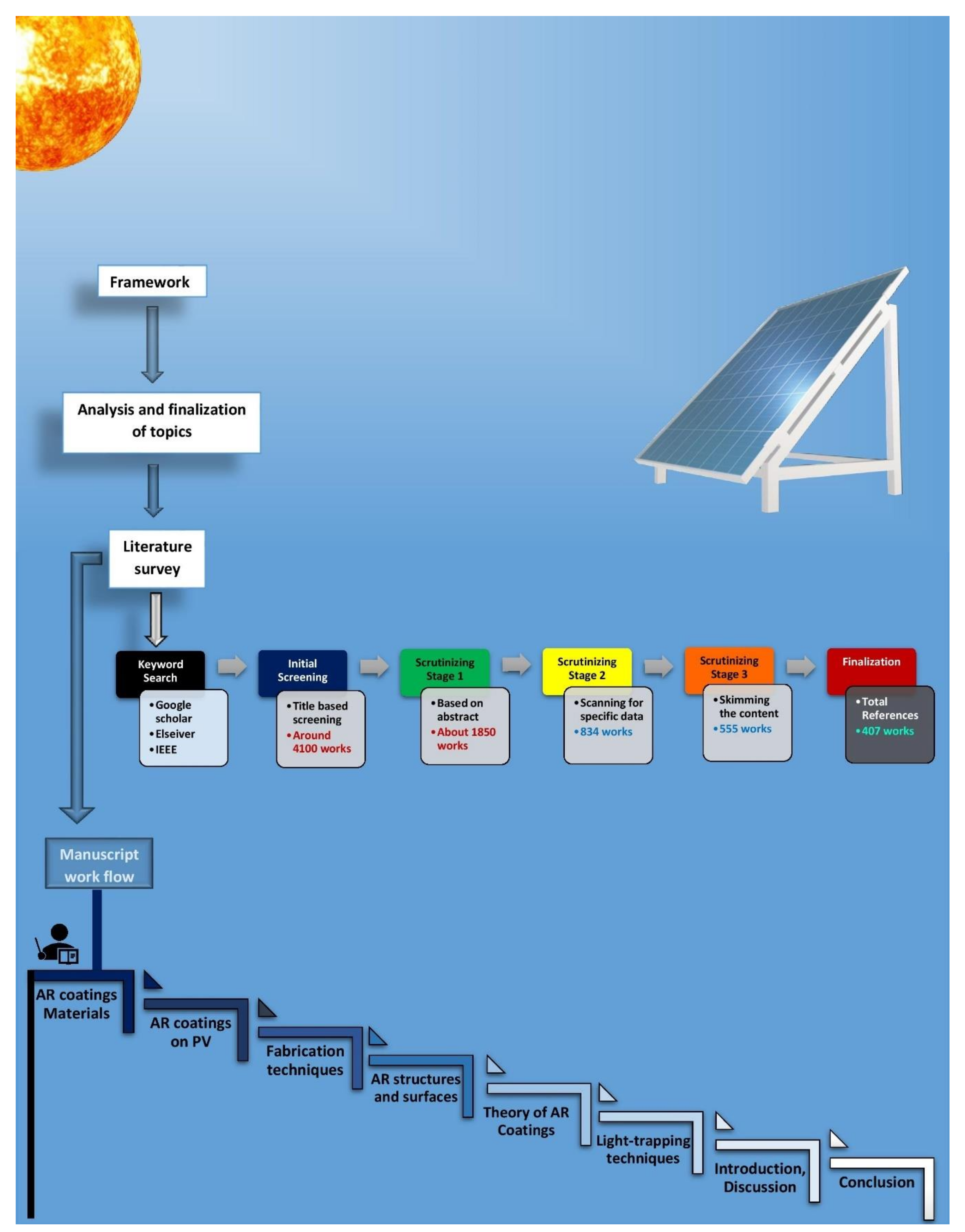
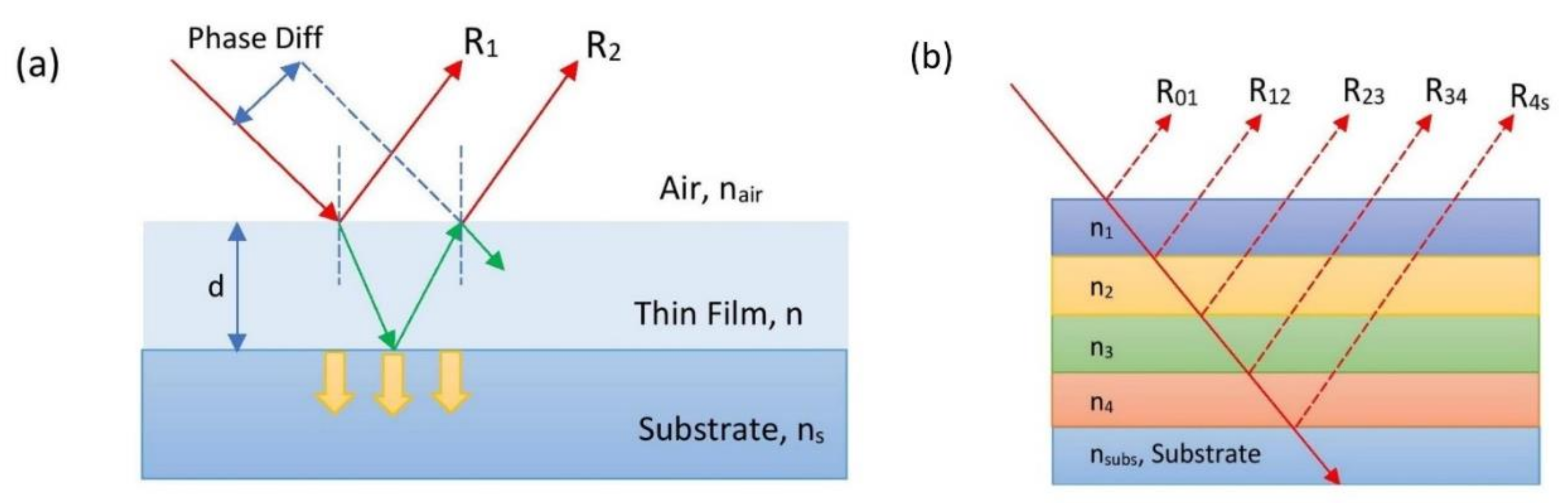
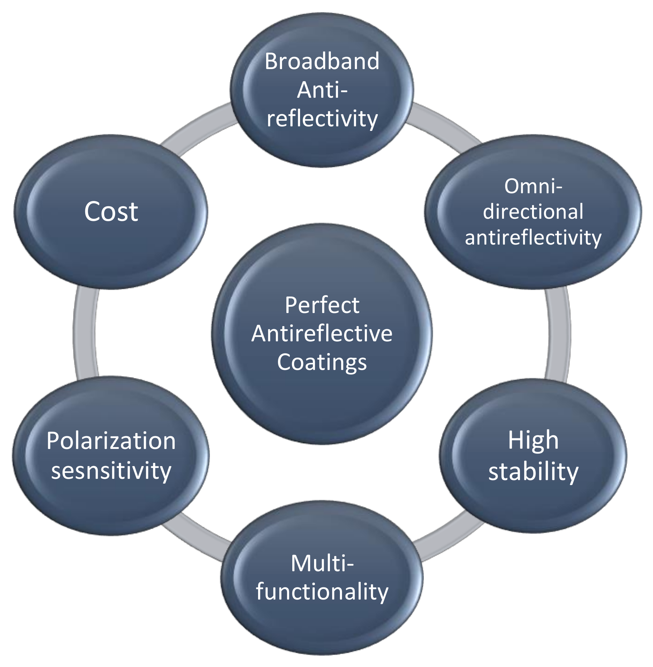
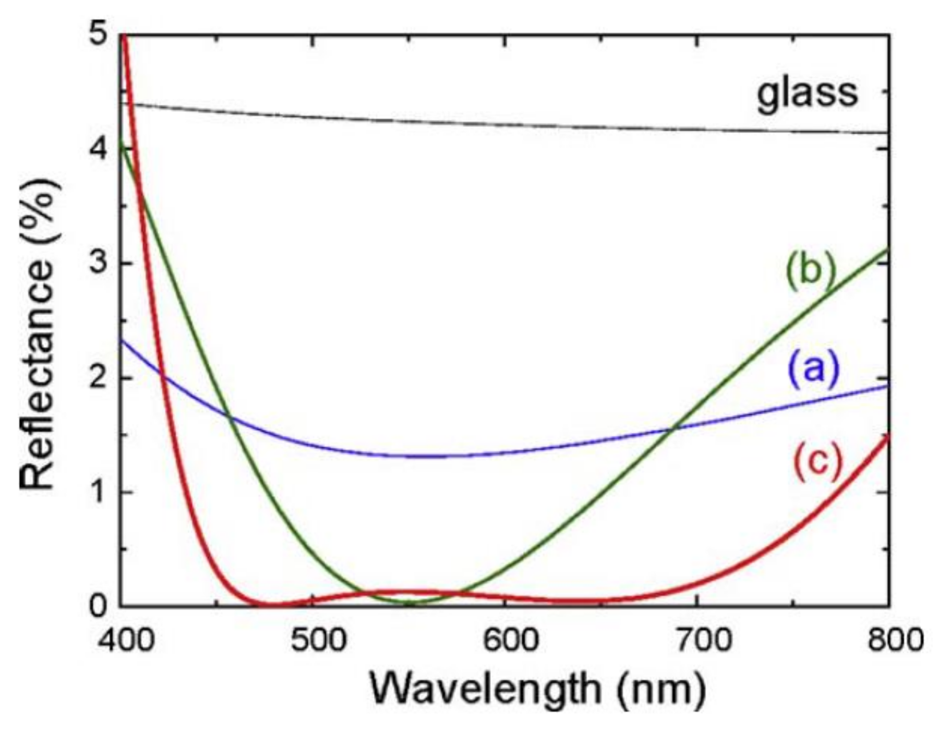
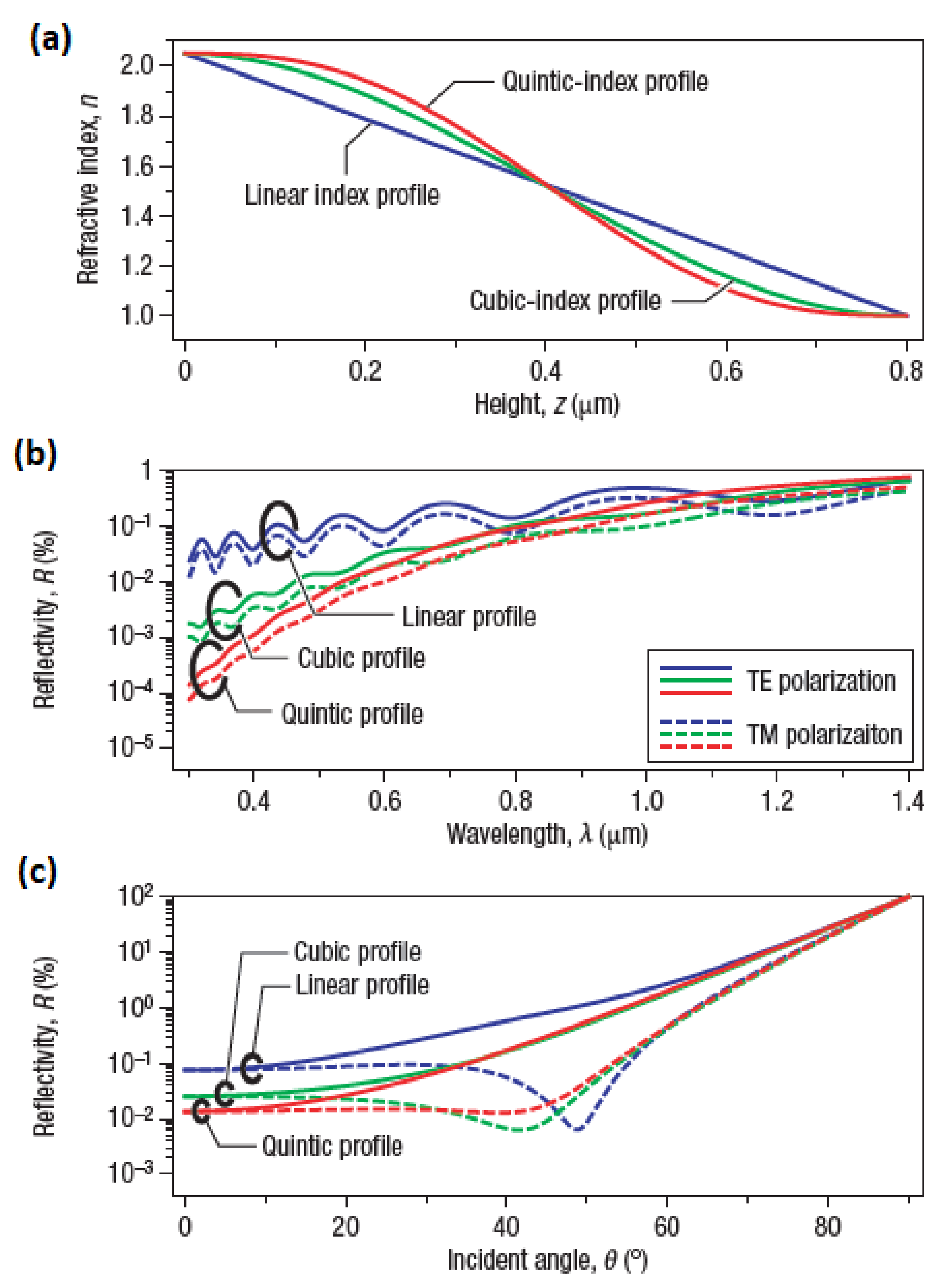
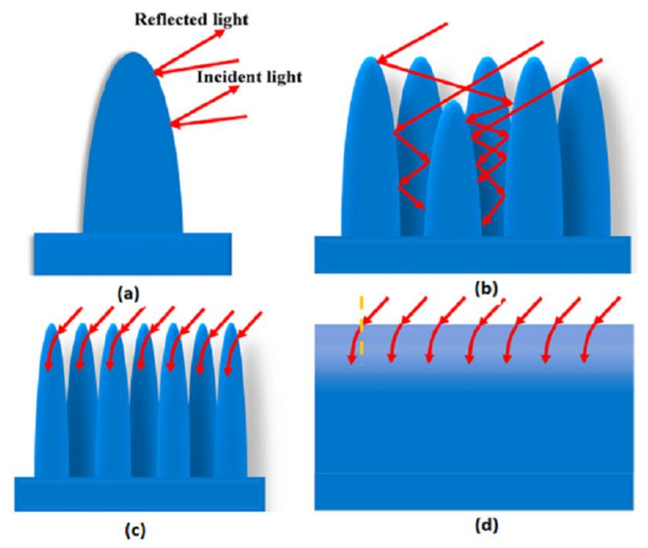
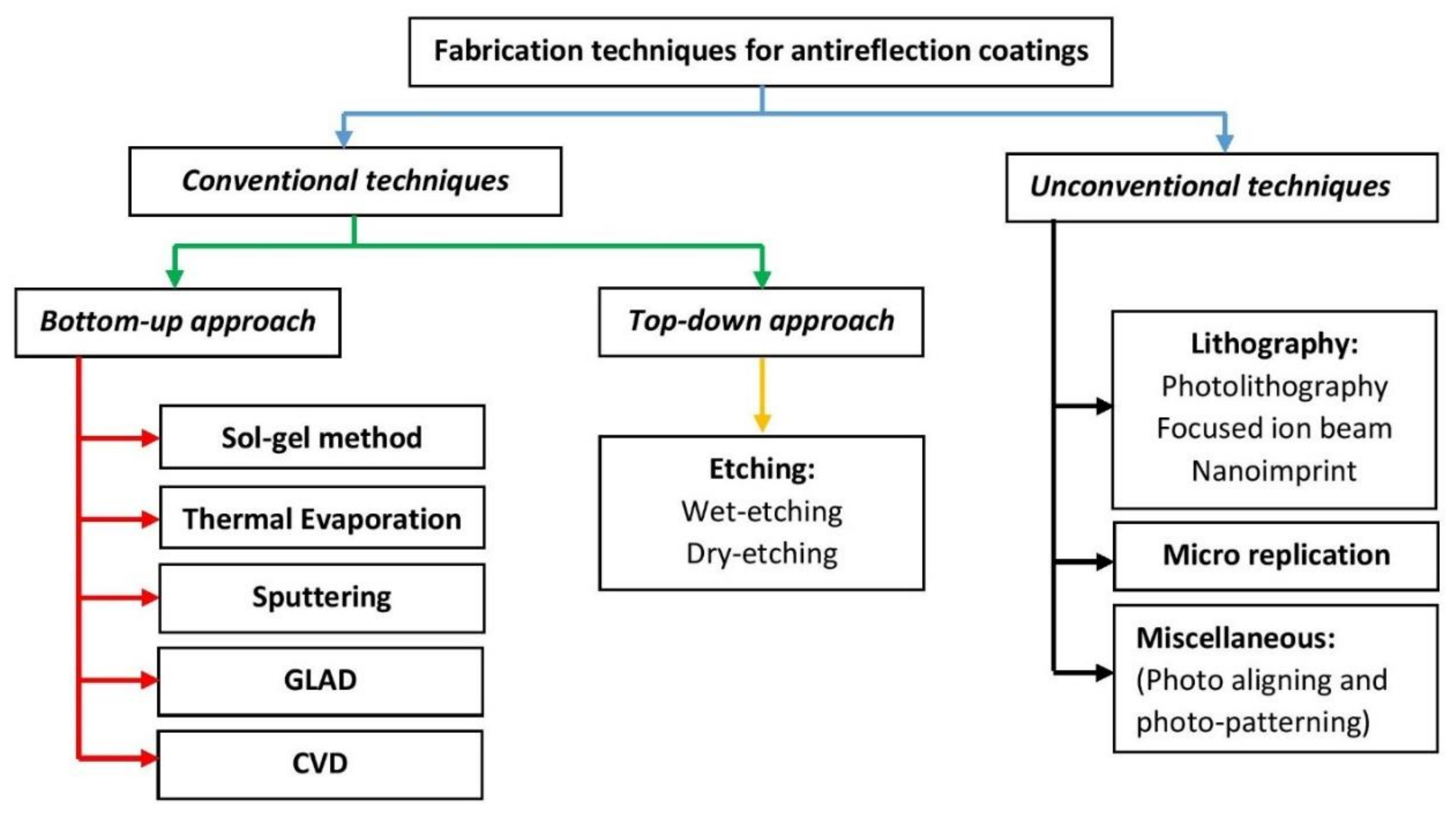
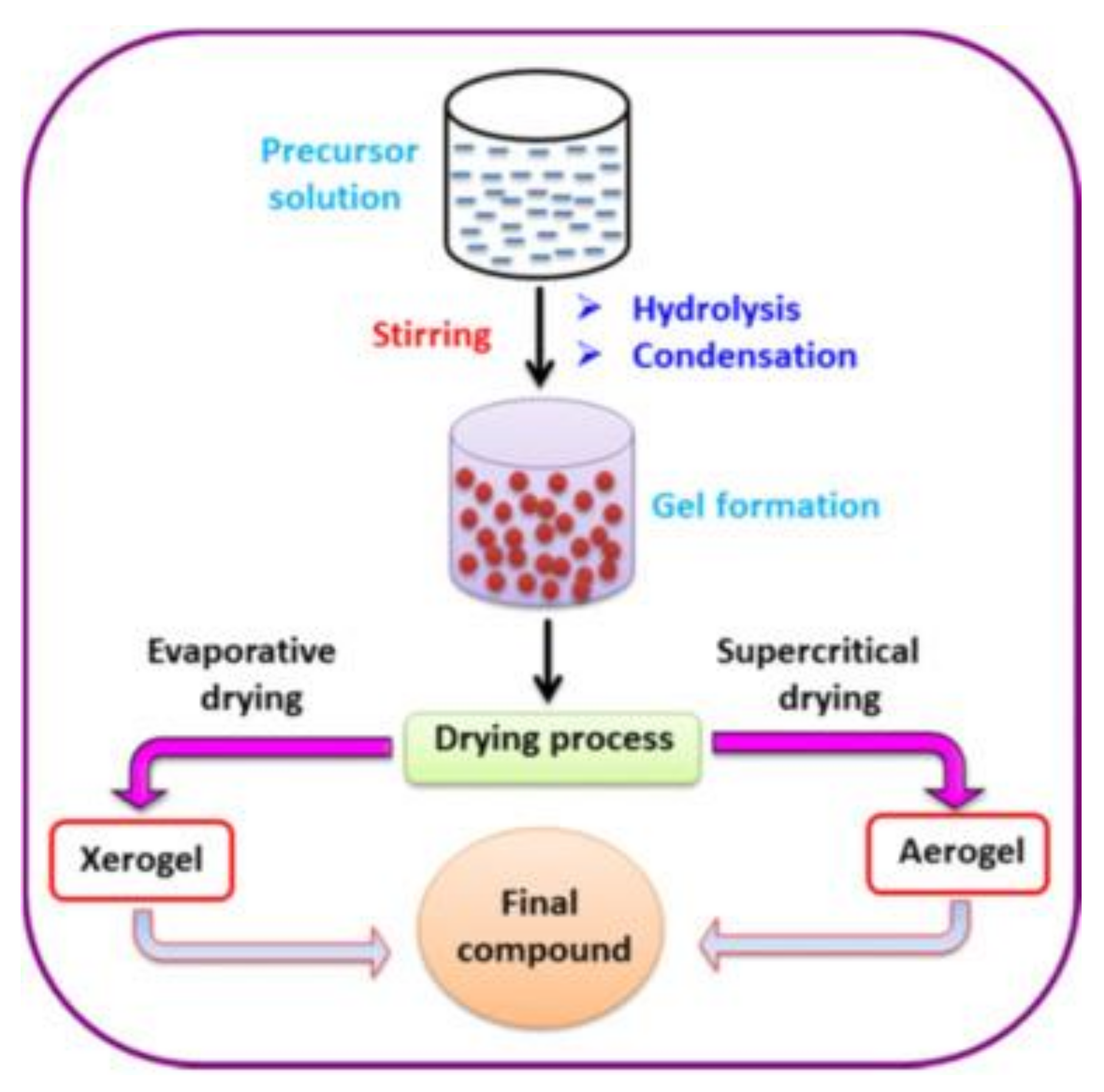
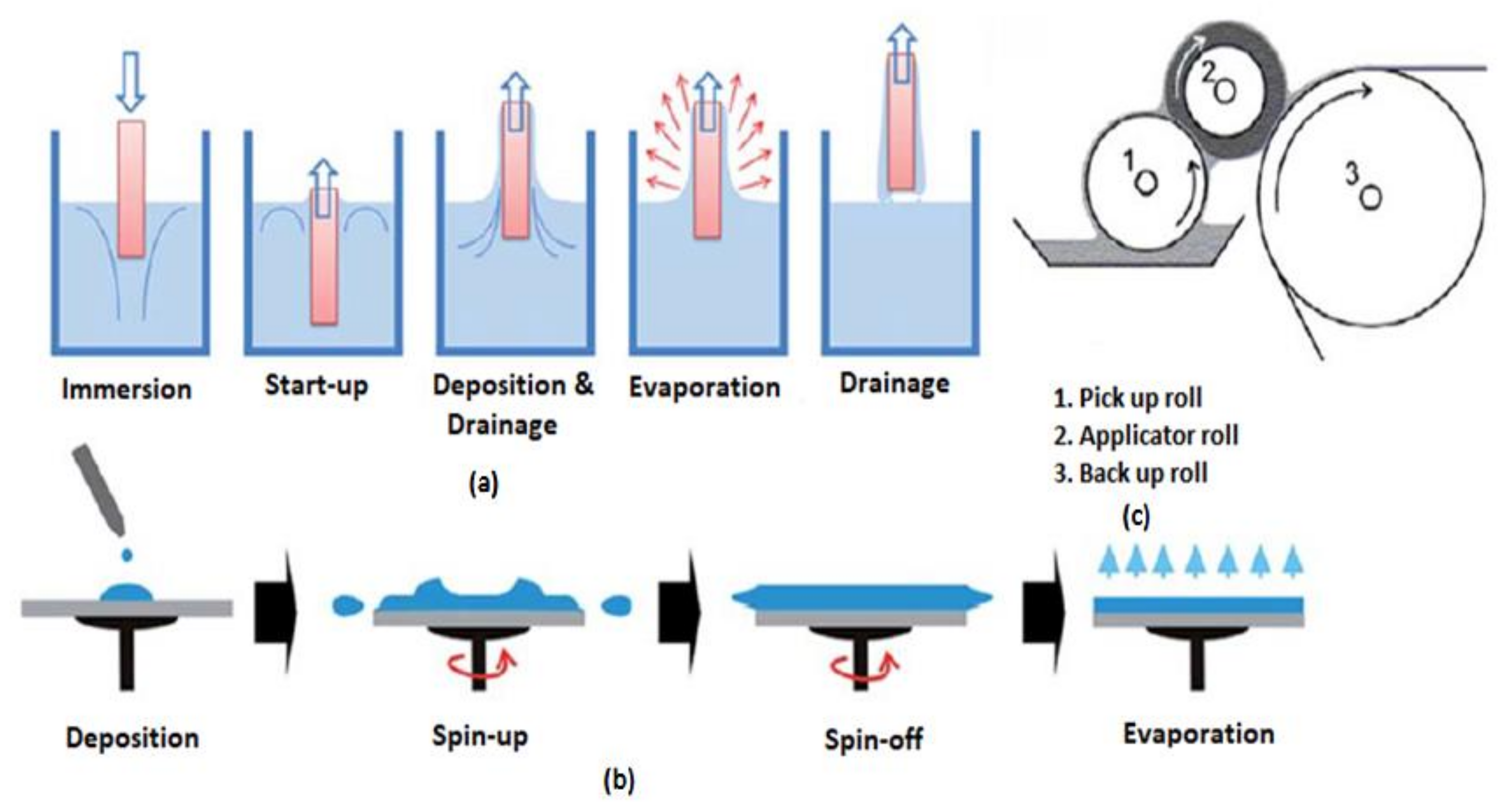
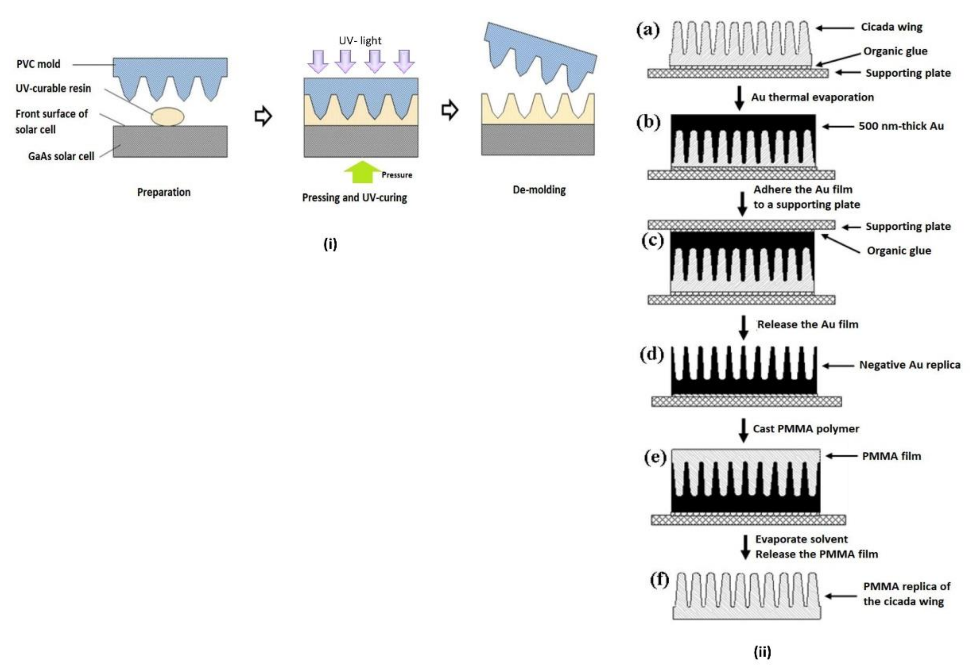
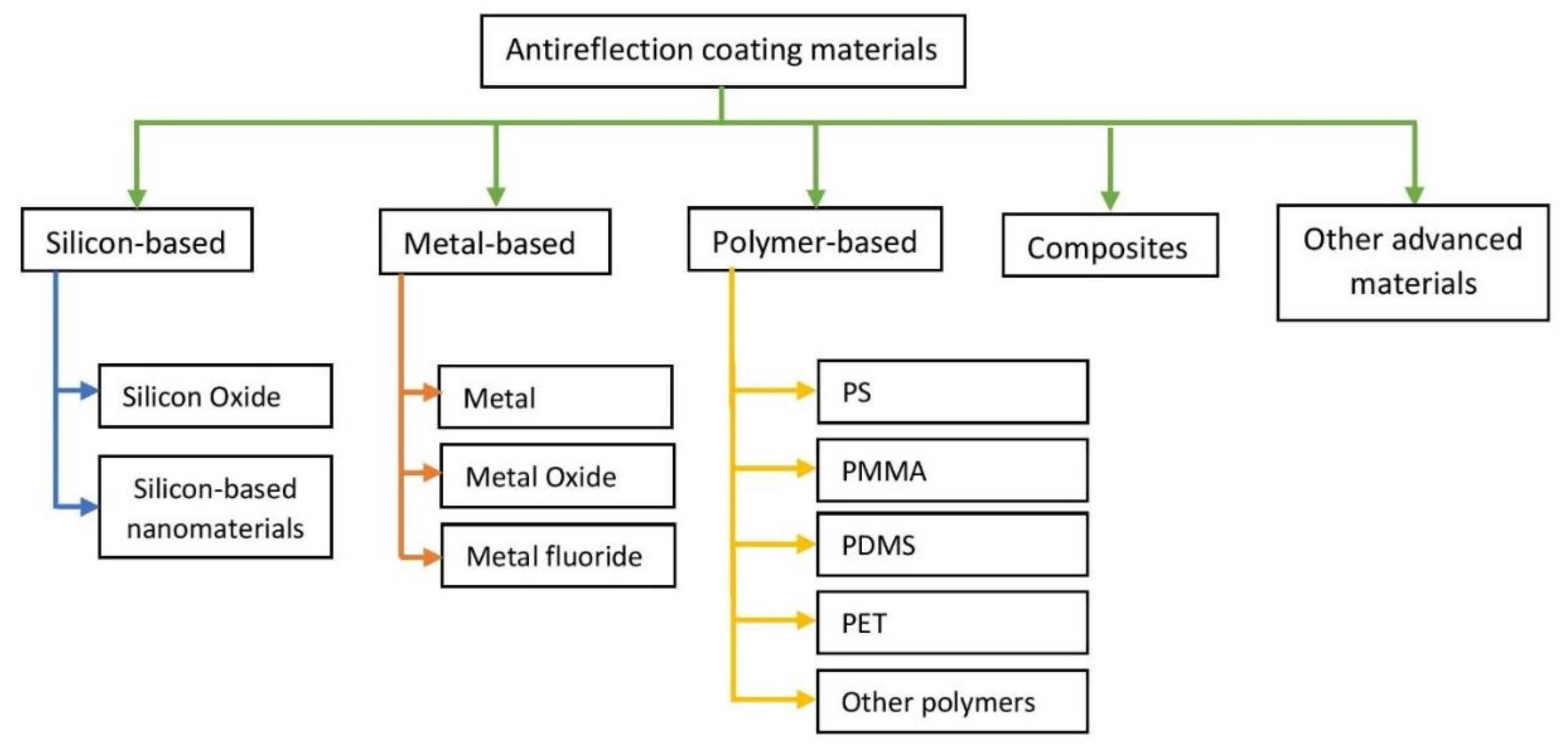
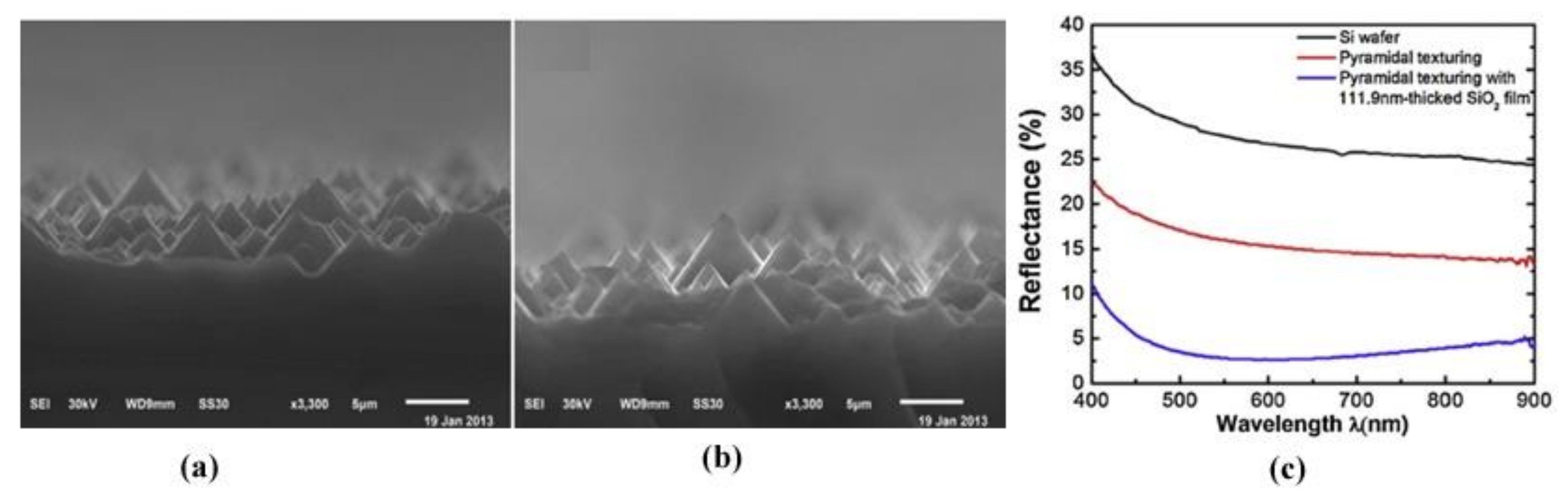
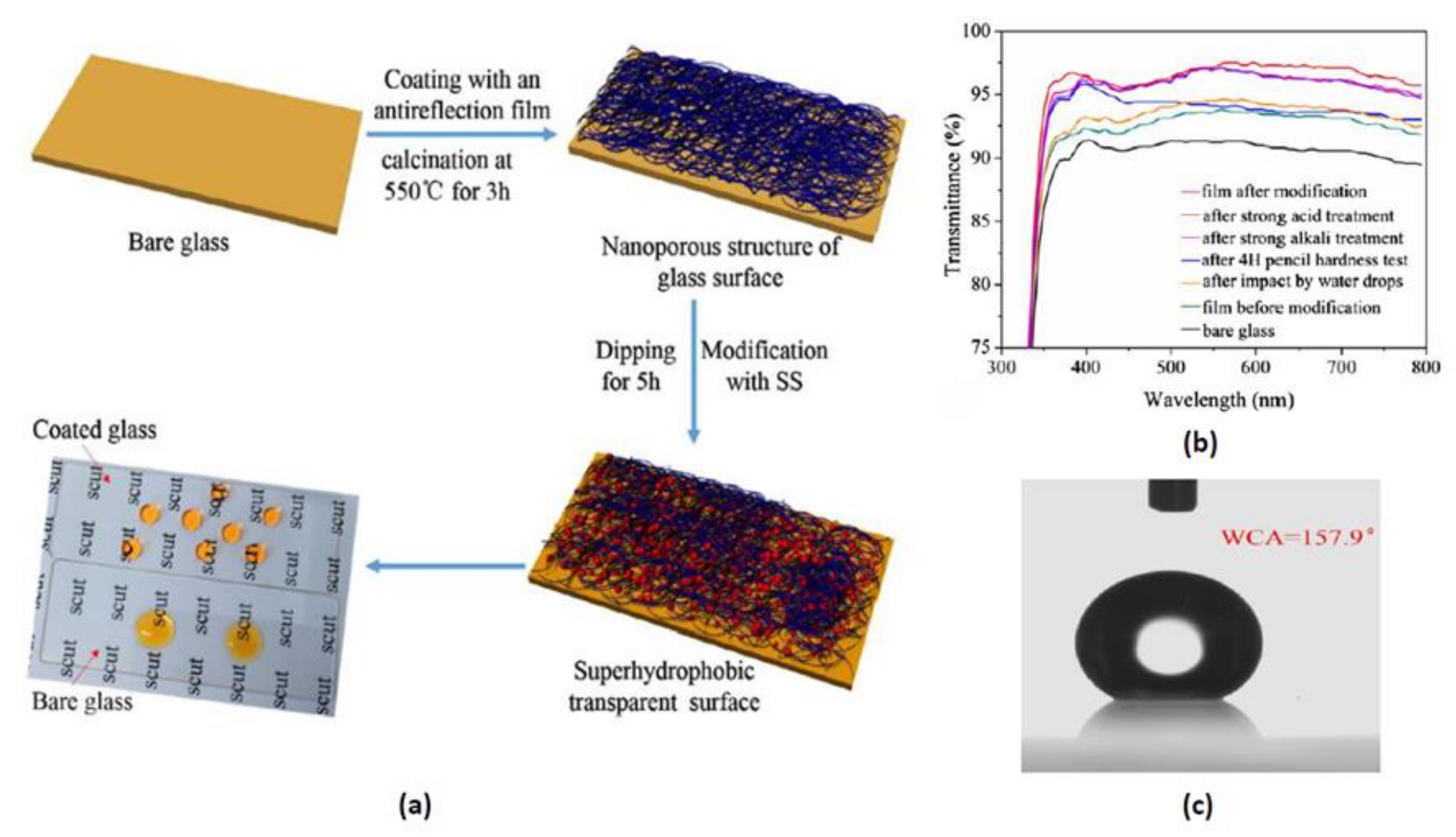
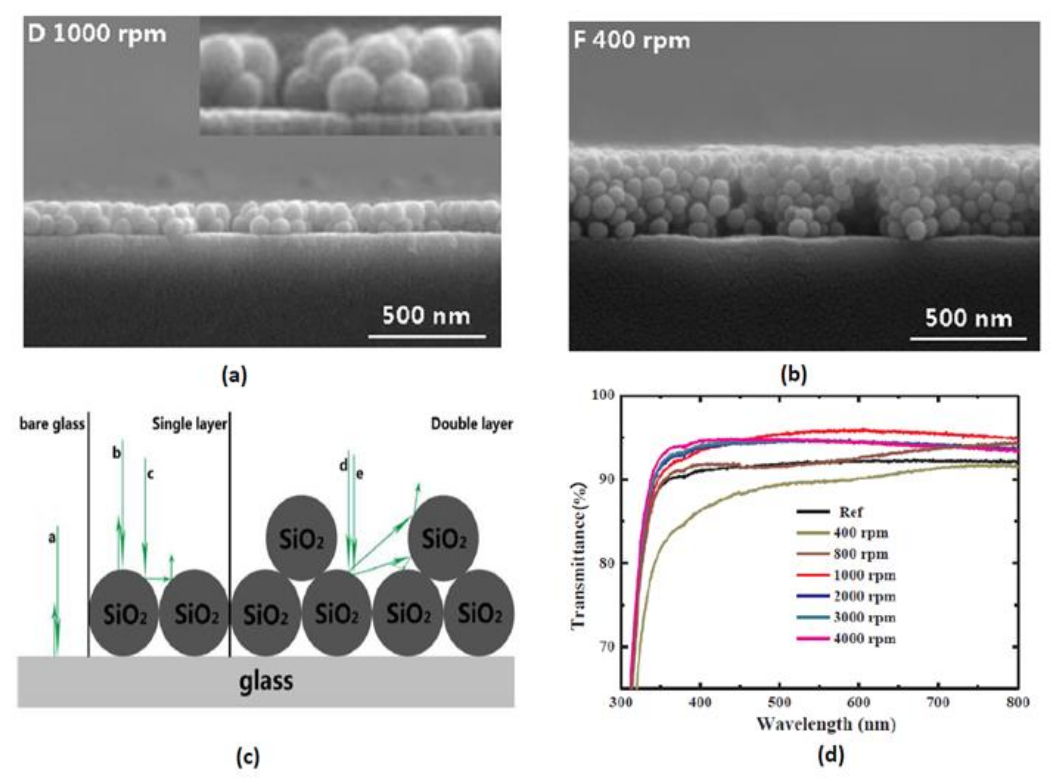
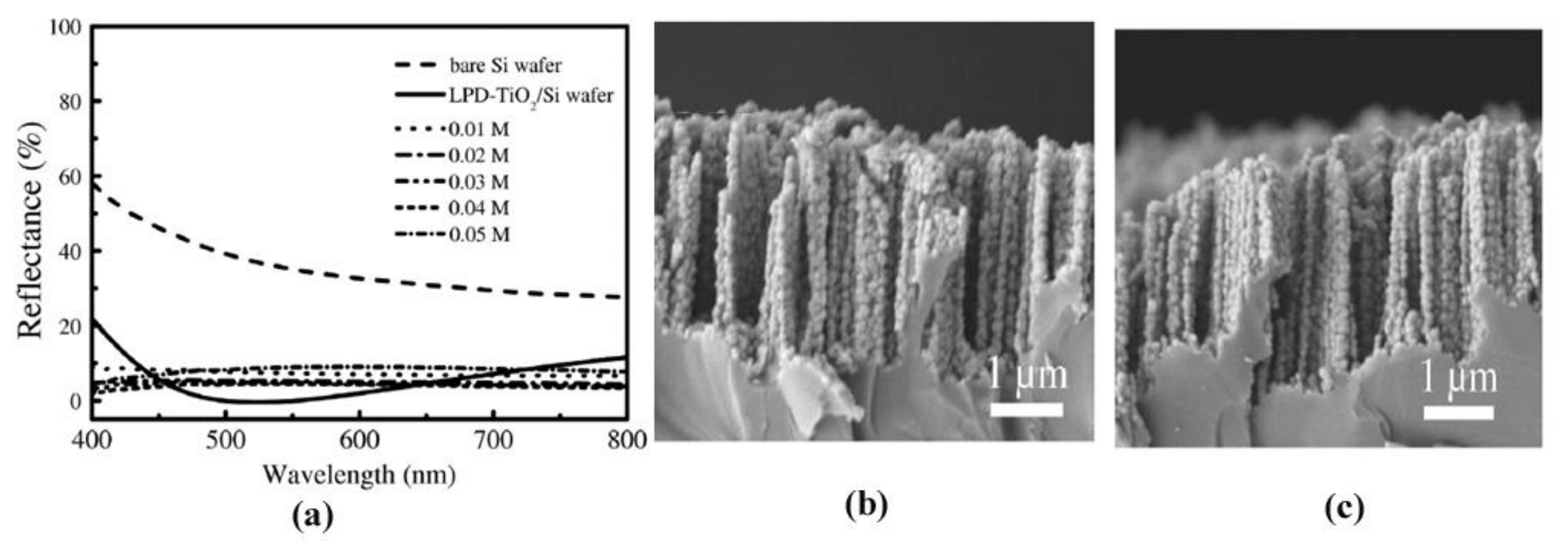
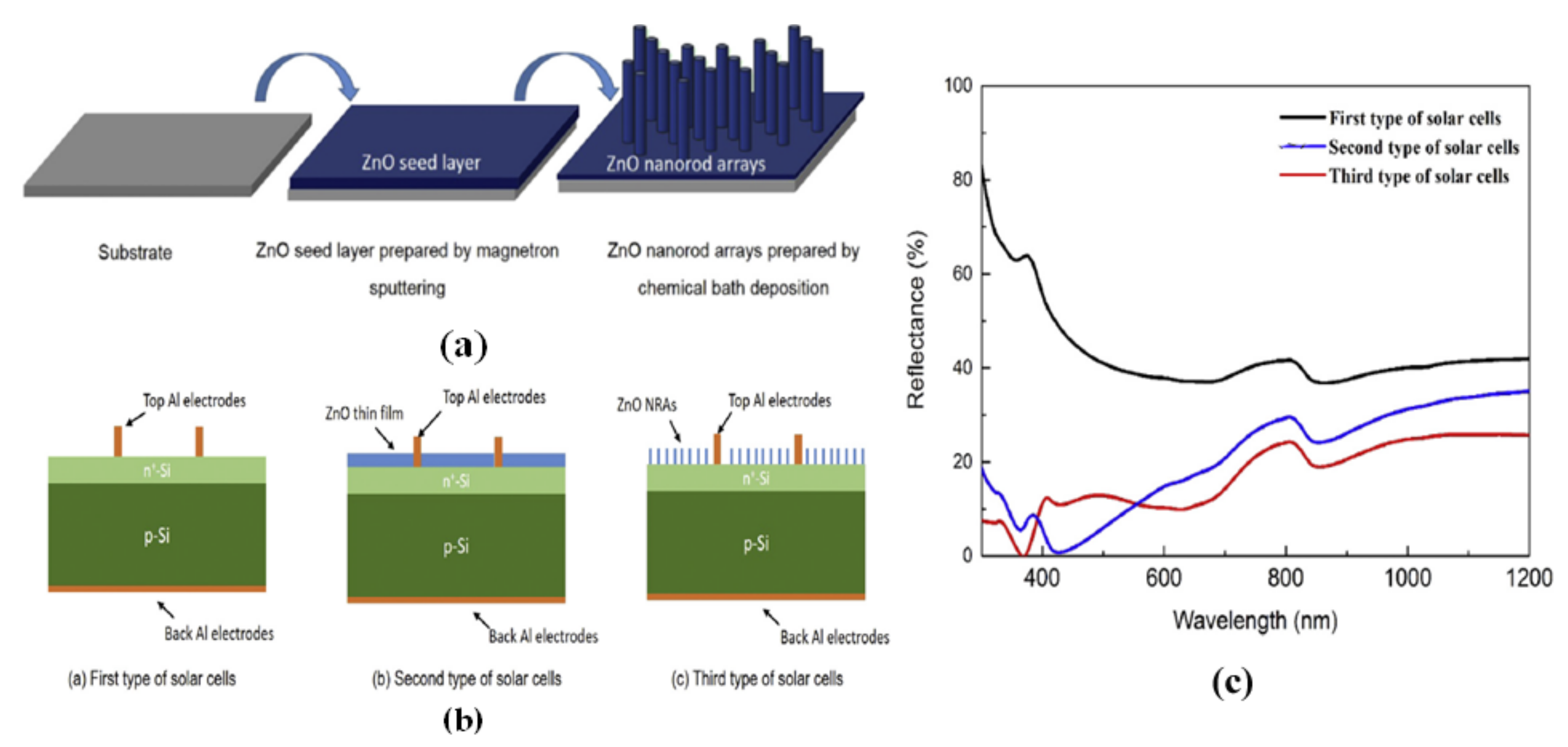
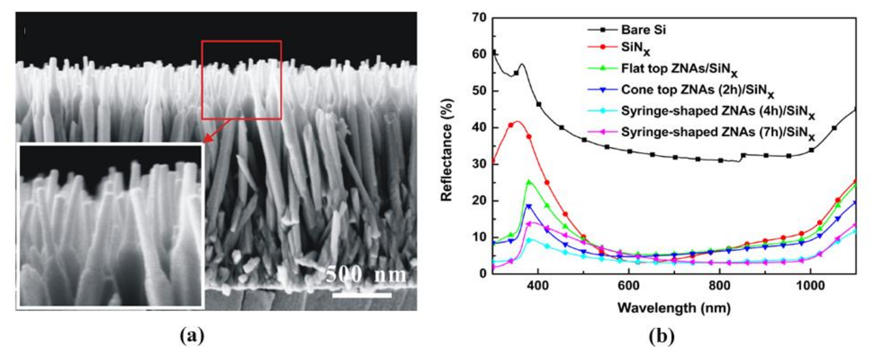
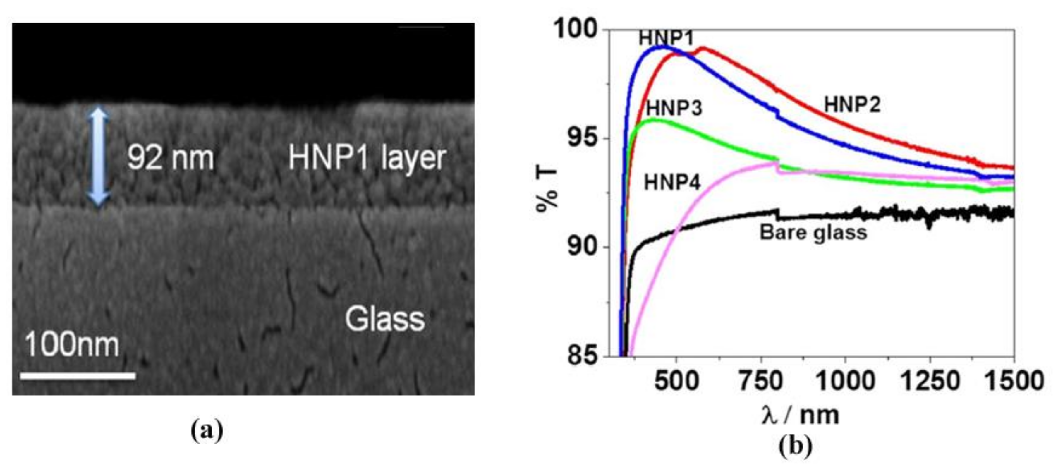
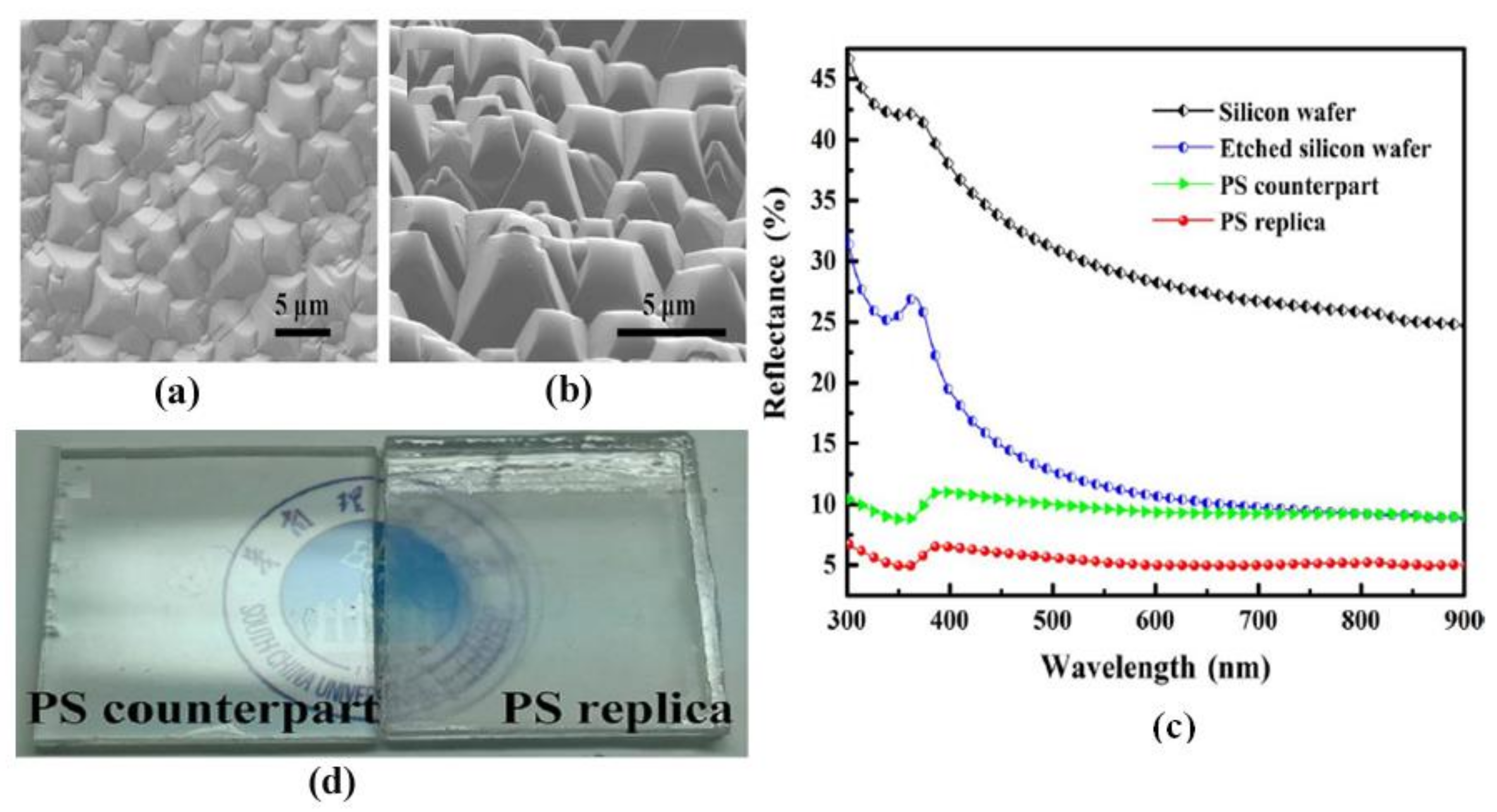
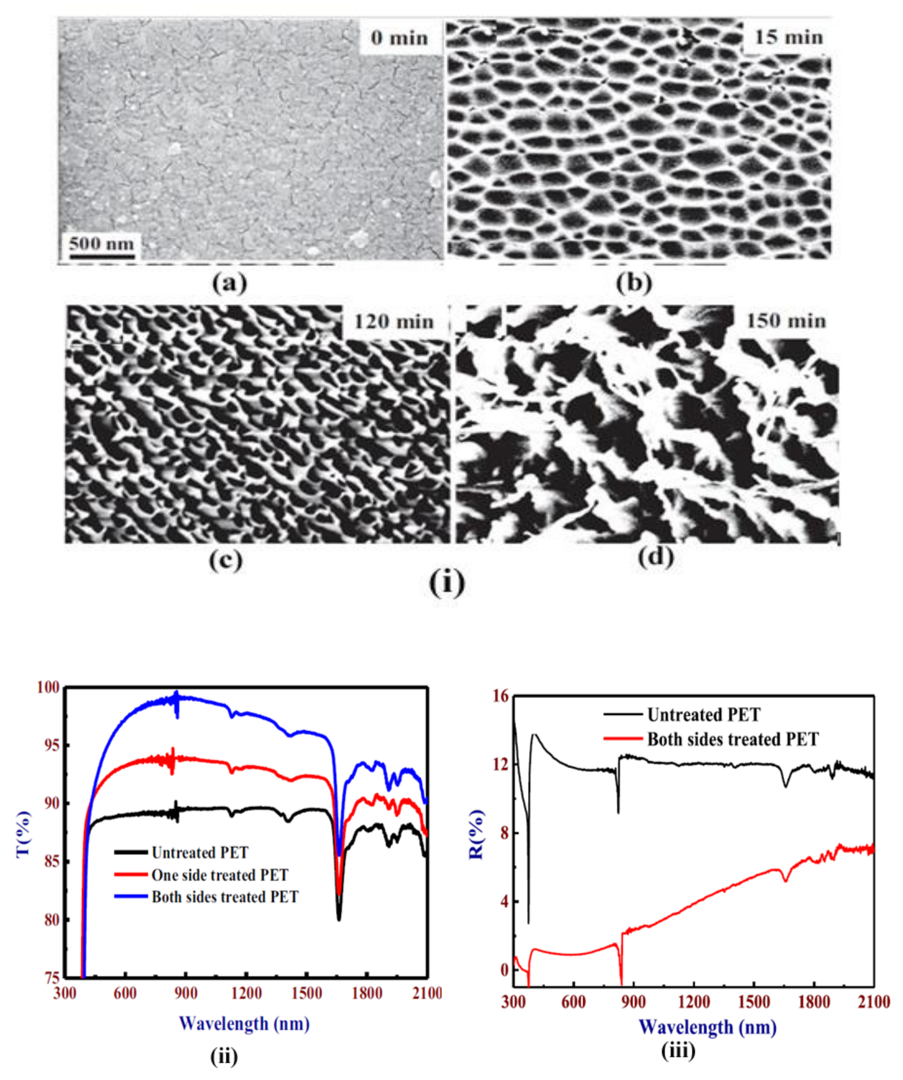
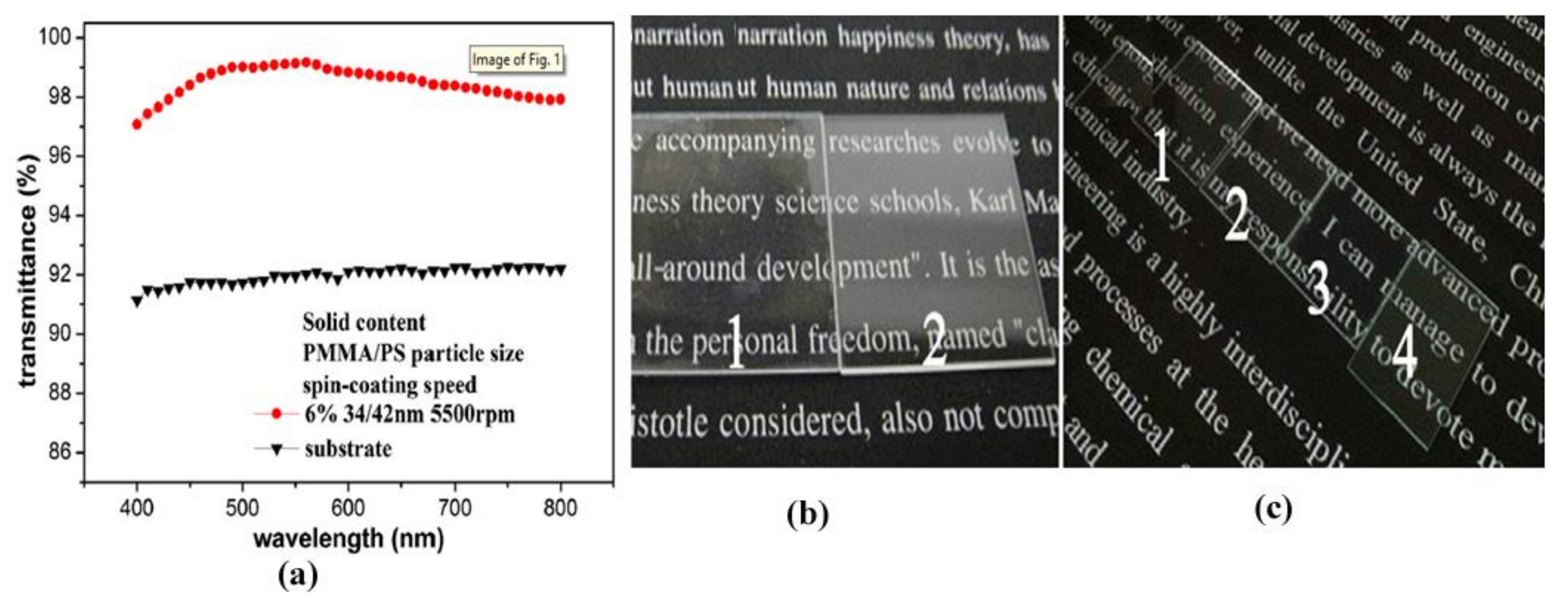
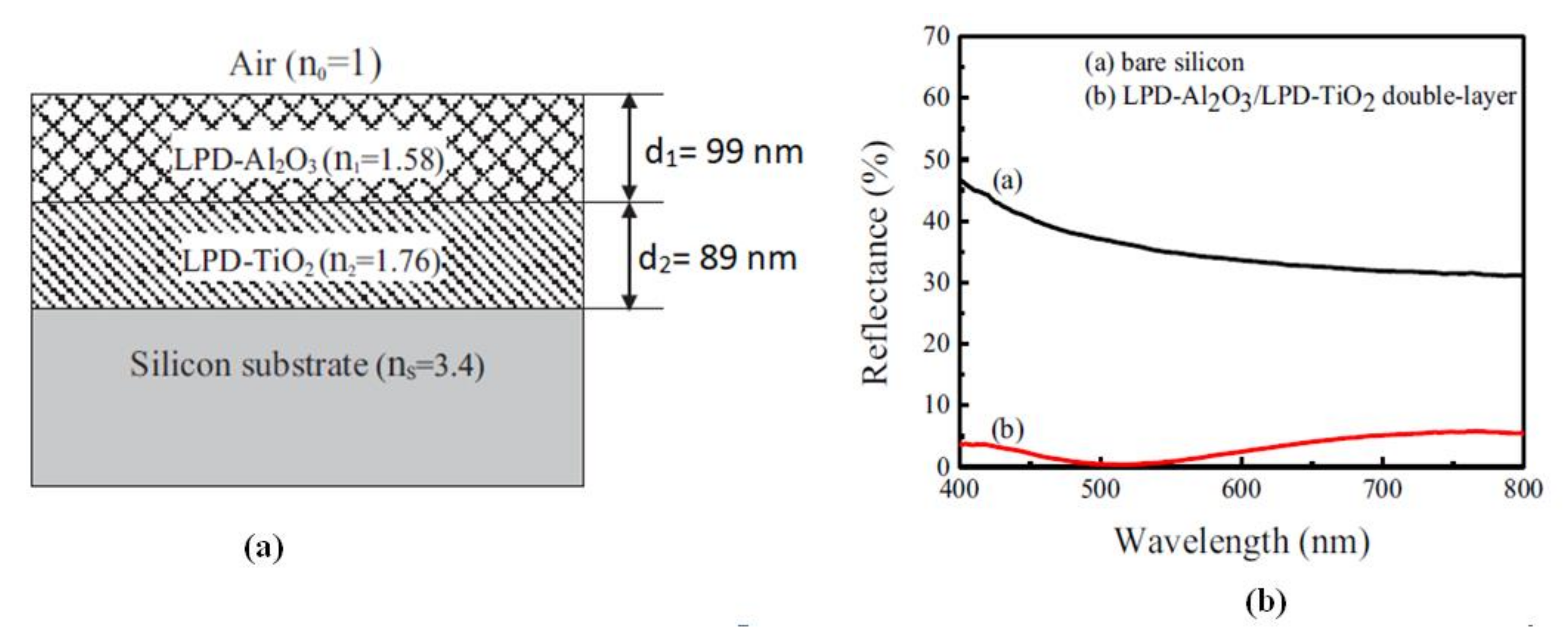
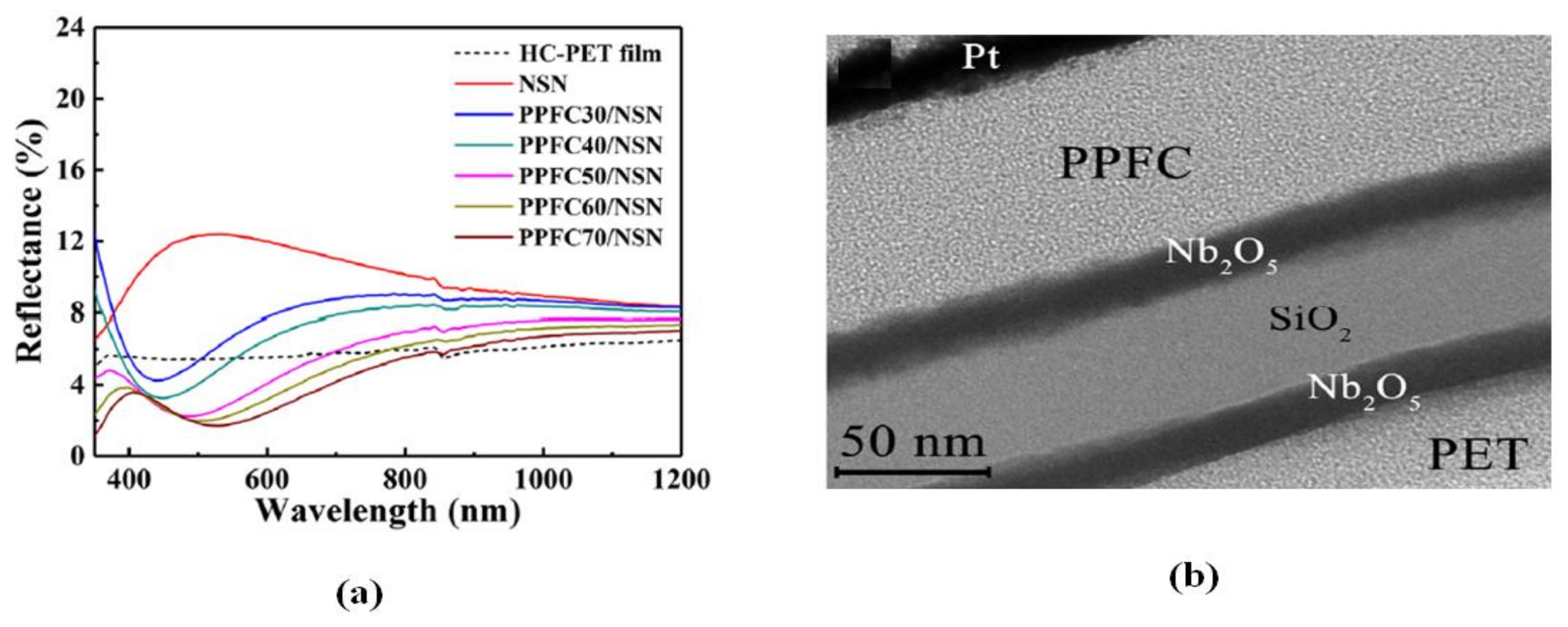
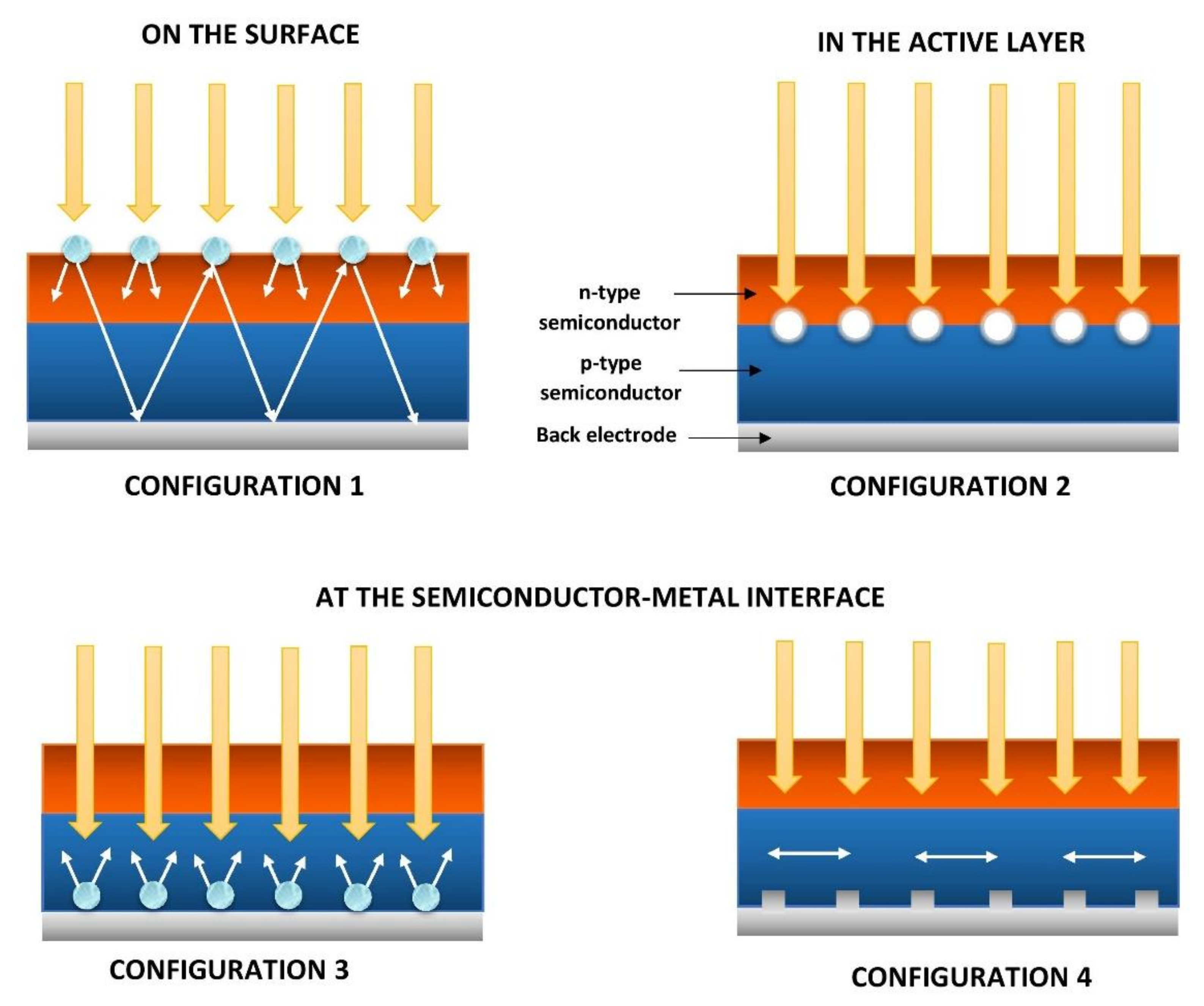
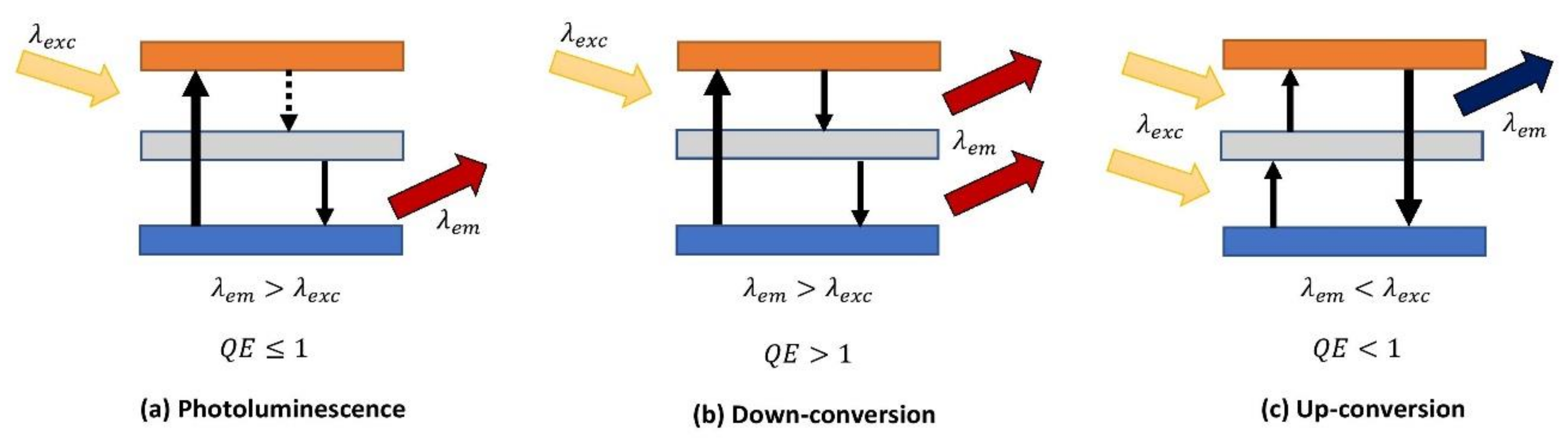
Figure 1. The framework of the study.
Energies 13 02631 g001
Figure 2. Schematic illustration of diffusion of light in (a) single layer film (ns > n) and (b) multiple layer film.
Energies 13 02631 g002
Figure 3. The various criterion for perfect antireflection coatings (ARCs).
Energies 13 02631 g003
Figure 4. Comparison of reflectance of (a) SLARC (b) DLARC (c) Three-layer ARC. Reprinted with permission [42]; 2010, Elsevier.
Energies 13 02631 g004
Figure 5. Comparison of various index profiles for gradient RI coating. (a) Variation of refractive index of linear, cubic and quantic -index profiles as a function of thickness (b) Variation of reflectance with respect to wavelength for linear, cubic and quantic-index profiles at normal incidence. (c) Variation of reflectance with respect to incident angle for linear, cubic and quantic-index profiles at 632.8 nm wavelength. Reprinted with permission [42]; 2010, Elsevier.
Energies 13 02631 g005
Figure 6. (a) Light interaction with macrostructure. (b) Multiple internal reflections resulted due to microstructure arrays. (c) Light interaction with nanostructure array. (d) Light interaction with GRIN structure resulting in bending of light rays. Reprinted with permission [36]; 2019, Elsevier.
Energies 13 02631 g006
Figure 7. Classification of commonly used fabrication techniques for ARCs.
Energies 13 02631 g007
Figure 8. The reaction pathway involved in sol-gel synthesis of metal oxide nanostructures. Reprinted with permission [74]; 2017, Elsevier.
Energies 13 02631 g008
Figure 9. Steps involved in various coating techniques (a) Dip-coating (b) Spin-coating (c) Meniscus-coating. Reprinted with permission [39]; 2016, Elsevier.
Energies 13 02631 g009
Figure 10. Typical thermal evaporation system representing resistive heating and electron beam heating. Reprinted with permission [75]; 2012, Elsevier.
Energies 13 02631 g010
Figure 11. (i) GLAD deposited microstructures (a) tilted structures, (b) Chevron or zig-zag structures, (c) helical structures, (d) vertical columns. (ii) (a) The angle of deposition α and the rotation angle of the substrate Ф to the deposition plane. (b) Typical GLAD apparatus implemented in the PVD system. (iii) Nuclei distributed across the surface leads to ballistic shadowing of the surrounding regions. Reprinted with permission [79]; 2007, AIP Publishing.
Energies 13 02631 g011
Figure 12. Schematic illustration of steps involved in photolithography.
Energies 13 02631 g012
Figure 13. (i) Illustration of various steps in the preparation of moth’s eye pattern using nano-imprint lithography methodology. Reprinted with permission from Ref. [93]; Copyright 2011, Elsevier (ii) Stepwise illustration of bio-replication method with cicada wing as a template. (a) Cicada wing structure. (b) Depositing Au on the Cicada wing structure through thermal evaporation. (c) Adhering the Au film to the supporting plate. (d) Releasing the Au plate to obtain the Au mold. (e,f) Replicating the cicada wing structure on the PMMA film through prepared Au mold. Reprinted with permission [42]; 2010, Elsevier.
Energies 13 02631 g013
Figure 14. Classification of antireflection coating materials.
Energies 13 02631 g014
Figure 15. Pyramidal textured SiO2 surface (a) before and (b) after thermal oxidation. (c) Comparison of reflectance in terms of wavelength for Si wafer surface, pyramidal textured Si surface without and with SiO2 coating Reprinted with permission [105]; 2015, Elsevier.
Energies 13 02631 g015
Figure 16. (a) Illustration of various steps in fabricating durable anti-reflection transparent superhydrophobic surfaces. (b) Comparison of transmittance for glass substrates with various coatings and without coatings with respect to wavelength. (c) Water droplet contact angle on the superhydrophobic coating. Reprinted with permission [116]; 2018, Elsevier.
Energies 13 02631 g016
Figure 17. (a,b) FESEM images of spherical SiO2 coating deposited on glass substrates with various spin-coating speeds. (c) Schematic illustration of the light interaction with SiO2 sphere-based ARCs. (d) Variation of transmittance for spherical SiO2 based AR coatings on glass substrate at various speeds (Ref—Glass sample without coating). Reprinted with permission [119]; 2018, Elsevier.
Energies 13 02631 g017
Figure 18. (a) The reflectance curve of LPD-TiO2 thin film on SiNWs with different H3BO3 concentration in 400 to 800 nm wavelength range. (b) SEM cross-sectional images of LPD-TiO2 (0.3 M)/SiNWs/Si, (c) LPD-TiO2 (0.4 M)/SiNWs/Si. Reprinted with permission [152]; 2017, Elsevier.
Energies 13 02631 g018
Figure 19. (a) Steps involved in the fabrication of ZnO nanorod arrays. (b) Schematic structures of fabricated three types of solar cells. (c) Variation of reflectance for the fabricated solar cells with respect to wavelength. Reprinted with permission [171]; 2017, Elsevier.
Energies 13 02631 g019
Figure 20. (a) Cross-section SEM image of the syringe-shaped ZnO nanorod arrays. (b) Comparison of reflectance of mc-Si PV cells with various surface conditions. Reprinted with permission [172]; 2018, Elsevier.
Energies 13 02631 g020
Figure 21. (a) FIB cross-sectional image of ARC consisting of hollow MgF2 nanoparticles (HNP-1 layer). (b) Transmittance spectra of AR films comprised of different hollow nanoparticles. Reprinted with permission [185]; 2018, Elsevier.
Energies 13 02631 g021
Figure 22. (a) Top and (b) tilted views of PS replica molded by micro-ICM (SEM images). (c) Comparison of reflectance spectra of silicon wafer, etched silicon wafer, PS counterpart, and PS replica. (d) Photograph of PS replica and PS counterpart exposed to white fluorescent light. Reprinted with permission [6]; 2017, Elsevier.
Energies 13 02631 g022
Figure 23. (i) FESEM micrographs of (a) untreated PET (0 min) (b) treated PET for 15 min (c) 120 min (d) 150 min; (ii) Transmittance spectra of untreated, one side treated and both sides treated PET. (iii) Variation of reflectance for untreated and both sides treated PET. Reprinted with permission [195]; 2016, Elsevier.
Energies 13 02631 g023
Figure 24. (a) Transmittance spectra of uncoated substrate and coated substrate in visible range (b) Images of substrate under bright light (1. Coated PMMA sheet; 2. bare PMMA sheet), (c) images of substrate under normal light (1. Uncoated PMMA sheet; 2. one-side coated PMMA sheet; 3. both sides coated PMMA sheet; 4. uncoated glass sheet). Reprinted with permission [213]; 2014, Elsevier.
Energies 13 02631 g024
Figure 25. (a) Structural diagram of double layer LPD-Al2O3/LPD-TiO2 ARCs. (b) Variation of measured reflectance for the LPD-Al2O3/LPD-TiO2 DLARCs on polished silicon substrate and bare silicon. Reprinted with permission [238]; 2015, Elsevier.
Energies 13 02631 g025
Figure 26. (a) Reflection spectra of HC-PET substrate film, trilayered NSN thin film, and quadrilayered PPFC/NSN thin films in 350 to 1200 nm wavelength range. (b) Cross-sectional TEM image of quadrilayered PPFC70/NSN thin film. Reprinted with permission [242]; 2019, Elsevier.
Energies 13 02631 g026
Figure 27. Various light-trapping configurations for plasmonic assisted solar cells.
Energies 13 02631 g027
Figure 28. Schematic illustration of various spectral modification methods.
Energies 13 02631 g028
Table 1. Various review works on antireflection coatings.
YOPTitle of the Review WorkOutcomeProvided Future Direction of ResearchReference
2020A review of anti-reflection and self-cleaning coatings on photovoltaic panels
  • Application of AR coatings on PV, various methods of preparation, material and surface aspects
  • Provided only the review of existing ARCs
[34]
2019Recent developments in multifunctional coatings for solar panel applications: A review
  • Self-cleaning and antireflective coatings for solar panels with their light transparency characteristics, surface morphology, electrical conductivity, and wettability
  • Polymeric AR and self-cleaning coatings developed using aqueous methods.
  • Smart hybrid coatings
[35]
2019Ascendant bioinspired antireflective materials: Opportunities and challenges coexist
  • The performance of bioinspired AR materials
  • Advantages, disadvantages, and limitations of various manufacturing techniques
  • Practical applications of ARC with nanostructures array
  • Challenges and opportunities of bio-inspired ARC
  • Natural novel structures, materials, and fabrication
  • Investigating a cost-effective, facile industrial method to prepare nano/micro-structured ARCs
[36]
2016Highly efficient antireflective and self-cleaning coatings that incorporate carbon nanotubes (CNTs) into solar cells: A review
  • Incorporation of CNTs into PV cell
  • Fabrication techniques for antireflection and self-cleaning coatings that include CNTs
  • Developments in AR and self-cleaning coatings involving CNTs
  • PCE comparison with allotropes of carbon and CNTs
  • CNT-polymer composites as electrode
  • Exploring in detail the optical characteristics of SWCNTs and DWCNTs
[37]
2016Antireflective surface inspired from biology: A review
  • Development of bionic antireflective structures
  • Fabrication techniques and the antireflective properties of bio-inspired structures
  • The challenge and prospects involved in bio-inspired structures
  • Optimization of materials performance
  • Environment-friendly and cheaper fabrication technology
[38]
2016Superhydrophobic surfaces with antireflection properties for solar applications: A critical review
  • Concepts of AR and self-cleaning coatings
  • Briefing AR surfaces with superhydrophobic properties
  • Mechanism and fabrication pathways of superhydrophobic and antireflective coatings
  • Challenges and future prospects
  • Surface formation mechanism and the composition, structure, and properties relationship analysis
  • Exploring cost-effective fabrication techniques for preparing high mechanical strength, abrasion-resistant ARCs
[39]
2014Recent progress in antireflection and self-cleaning technology—From surface engineering to functional surfaces
  • The basic principle, fabrication strategies and material aspects of self-cleaning AR coatings
  • The practical applications of self-cleaning ARCs with future development
  • Theoretical simulation to reveal the fabrication mechanism and to relate composition, structure, and properties
  • Environmental issues-oriented research for ARCs
[40]
2011Anti-reflective coatings: A critical, in-depth review
  • Strategies adopted for attaining antireflection and types of ARCs
  • Various fabrication methods and materials used
  • Challenges in AR coatings
  • Research towards decreasing the gap between affordability and durability
[41]
2010Anti-reflecting and photonic nanostructures
  • Structure and surface analysis of ARCs
  • Design and construction of photonic nanostructures
  • Material aspects and future trends of ARC
  • Antireflection coatings on deformable substrates and the application of CNTs
[42]
Table 2. Comparison of various fabrication technologies commonly used for antireflection coatings.
Fabrication TechniquesControlling ParametersType of Coatings Commonly FabricatedFacilenessUniformity of the Deposited CoatingFilm QualityDeposition Rate or Rate of FabricationCostAdvantagesDisadvantages
Sol-gelType of precursors, the concentration of precursors and additives, solvent nature, pH of the solution, pre- and post- heat treatmentMetal oxide and dielectric (silica) thin films, nanoporous filmsYesDepends on the coating used and the controlling parameters. Spin coating yields higher uniformityHigh homogenous films can be obtainedVery fast depositionLow-costSimple, fast, low temperature, and inexpensive techniquePrecise control in tuning the morphology and reproducibility is difficult
Thermal EvaporationPressure and substrate heat are the prime parameters. Also, the process can be assisted with microwave, plasma or electron resonance to have more controlPreferably low melting point metals and dielectricsYesUniformity is lessHigh impurities but low in case of E-beam heatingModerate deposition rate (10–100 nm/min)Cost-effective in large-scale productionFacile method of deposition, suitable for large-scale implementation, good reproducibility and scalable methodPoor uniformity, low dense films and becomes expensive when E-beam is used
SputteringIntense of vacuum pressure, sputter gas pressure, substrate and target temperature and sputter powerBoth metal and dielectric porous and thin filmsNoExcellent uniformityLess impurities and high-quality filmsVariable depositing rates depending on the type of sputtering usedExpensiveHigh-quality films, wide variety of materials can be deposited, scalable methodRequires sophisticated arrangements and cost-ineffective
Glancing angle depositionVacuum, deposition pressure, deposition rate, vapor flux incident angle and rotational speed of the substrateBoth metal and dielectric porous filmsYesUniformity is lessModerate to high quality structures can be formedVariable deposition rateModerate costMorphology and porosity can be accurately controlled. Highly suitable for porous filmsLow dense films
PECVDSubstrate material and temperature, gas composition, flow rate, temperature and pressure, frequencyMainly dielectric thin and porous filmsNoGood uniformityVery low impurities and high-quality filmsVariable and high deposition rateExpensive but APCVD is less expensive comparativelyIndustrial method, high deposition and uniformity, easily coated even on textured substratesExpensive method, high operating temperature
Wet EtchingConcentration of etchant, temperature and rate of waste product removalTextured surfacesYesIsotropic etching results in uniform etching-High etching rate. It depends on the etchant usedLow-costHigh selectivity, high etching rate and straight forward method. Often, used with other fabrication methodsMost cases are mask-assisted to protect the substrate and no precision control
Dry EtchingChamber pressure, gas flow rate and bias controlTextured surfacesYesUniformity is obtained in tradeoff with rate and selectivity-Etching rate depends on gas or ions usedLow-costCheap and eliminates the use of dangerous solvents and acidsNo precision control and some employed gases are corrosive and toxic
LithographyResist film thickness and uniformity, exposed radiationWide variety of structures and surfacesNoDepends on the etching after lithographic exposure--Depends on the radiation used. Low-cost approaches existProcess parameters can be precisely controlled. Time efficient, simple and high throughputSophisticated equipment is required. Inefficiency in generating 3D structures
Nano imprint lithographyPrecision of the mold, applied pressure.Wide variety of structures and surfaces, and biomimetic coatingsYesHigh uniformityQuality of the structures depends on the moldRapid fabrication if mold is readyCost-effective in large-scale productionSimple, cost-effective, time-effective and large area fabrication is possibleUsually, the cleaning of the compressed resist demands reactive ion etching process. Mold fabrication requires advanced technologies
Soft lithographyDepends on the elastomeric stamp, temperature and pressure appliedWide variety of nano-structures and surfaces. Preferably polymer coatingsYesExcellent surface uniformityGood quality structuresRapid fabricationLow-costSimple, fast, good adhesion, high resolution with high precisionIt depends on lithography techniques to create master patterns
Table 3. Silicon based antireflection coatings.
AR Coating MaterialARC StructureFabrication TechnologyReflectance (%)Transmittance (%)Wavelength (nm)FeaturesResearch PotentialReference
SiliconNanowires (NWs)Ag catalyzed chemical etching5.6-250–800Large scale SiNWs arrays can be prepared using MACE methodExperimental analysis of the increase in PCE using this coating[111]
Porous silicon (PSi)
(i)
Single layer PSi
(ii)
Doube layer PSi
Electrochemical process
(i)
~7
(ii)
~3
-400–1000Porosity can be varied by modulating current density in the electochemical processEffect of this coating on various solar cells to find its suitable application[102]
Porous silicon (PSi)Double PSi layerChemical stain etching5.8-400–1100Low reflectivity comparable to SiNx coatingEffect of this coating on various solar cells to find its suitable application[103]
Hydrogenated nanocrystalline SiNanorod arraysHigh frequency plasma enhanced vapor deposition<5-400–1100Broadband antrireflection coating with very low reflectanceExperimental analysis of the increase in PCE using this coating[121]
SilicaSingle layer nanoporousSol-gel dip-coating -97.5500Cost-effective and straight forward technique.Transmittance can be improved in the whole visible range[99]
SilicaDouble layer porous filmRemote PECVD-99.4400–1150The low refractive index of the order of 1.11 can be fabricatedPower conversion efficiency changes can be analyzed using this coating[100]
SilicaSingle layer SiO2Chemical etching and thermal oxidation15.6-400–900Uses pyramidal textured Si wafer on which SiO2 is depositedResearch can be performed to reduce the reflectance further[105]
Silica Closed-surface silica ARCAcid catalyst sol-gel method-97.1300–1200Robust mechanical properties with 5 H pencil hardness and high moisture and high-temperature resistanceEffect of this coating on various solar cells to find its suitable application[106]
Silica Multi-layer stacks of silicaSol-gel and evaporation induced self-assembly (EISA) technique-7.2% increase than bare glass300–2000Suitable for Concentrated photovoltaic (CPV) applicationStability, reliability and environmental effects of/on the coating can be analyzed[107]
Silica NanoporousDip or spray coating-3.1% increase than bare glass400–1100Large area and cost-effectiveARC for solar glassesTransmission can be enhanced further, and efficiency analysis can be made[112]
Silica NanocylinderSol-gel and softimprint lithography0.57-425–700Large area fabrication, cost-effective, and simple methodsImprovement of transmittance in broadband wavelength range and efficiency analysis can be considered[113]
SilicaFour-layer Nano-porous SiO2Glancing angle deposition technique0.04-400–800Very negligable reflectanceExperimental analysis of the increase in PCE using this coating[114]
Silica Five-layer hollow silica nanoparticlesDip coating method-99.04380–1600Broadband antrireflection coatingEffect of this coating on various solar cells to find its suitable application[115]
Silica NanoporePhase separation process, calcination, dip coating-97400–800The coating is resistant to water, strong alkali and acids possessing 4H pencil hardnessExperimental analysis of the increase in PCE using this coating[116]
Silica NanoparticlesStober and dip coating method-99.9550Robust and self-cleaning ARCsEffect of this coating on various solar cells to find its suitable application[117]
Silica Double function SiO2-DMS coatingSol-gel method-96.07300–800Fluorine-free materials were used as a modifier to obtain water repellent capabilityEffect of this coating on various solar cells to find its suitable application[118]
Silica NanosphereSpin coating -3.8% increase400–800PCE improved from 14.81 to 15.82% for PSC deviceImprovement of transmittance in broadband wavelength range and stability, the durability of the film can be considered[119]
SilicaMoth-eye like structureSol–gel dip-coating and electrostatic self-assembly technique-8.21% increase400–800PCE is icreased from 11.66% to 12.59% for CIGS deviceStability, durability and environmental effects of/on the coating can be analyzed[120]
Mesoporous silicon + SiOx layer
(i)
single layer Psi
(ii)
PSi layer + SiOx layer
Plasma enhanced chemical vapour deposition
(i)
9
(ii)
3.8
-400–1000Passivation property is also improvedExperimental analysis of increase in PCE using this coating[83]
SiO2 with boron doped Zinc oxide (BZO) substrateSiO2 AR coatings/glass/BZOSol-gel dip coating method-93.4400–1000The efficiency of the amorphous thin film Si PV cell enhanced from 9.83% to 10.24%Stability, reliabilty and environmental effects of/on the coating can be analyzed[104]
Silicon nitrideSingle layer SiNx on textured Si waferPlasma deposition2.597300–1000Good optical and excellent passivation propertiesStability, durability and environmental effects of/on the coating can be analysed[122]
Silicon nitrideSiNx coating on multicrystalline silicon waferPlasma texturization and chemical etching<10-350–800Perfomance enhancement of mc-Si solar cellsA comparative study with other ARC can be made considering, cost-effectiveness and efficiency enhancement[123]
Table 4. Metal based antireflection coatings.
AR Coating MaterialARC StructureFabrication TechnologyReflectance (%)Transmittance (%)Wavelength Range (nm)FeaturesResearch PotentialReference
AuNanocone arraysGold vapor deposition<1-450–950Broadband antireflective and light-absorbing propertiesEffect of this coating on various solar cells to find its suitable application[131]
TiO2Thin filmAtmospheric pressure chemical vapor deposition8.61-300–1150Simple, inexpensive methodology and attains a +3% gain in PCE relative to the reference cellStability, reliabilty and environmental effects of/on the coating can be analysed[147]
TiO2Porous film Sol-gel based self-assembly and plasma-based approach-95400–900Usage of a novel fabrication method involving a low-cost block copolymerExperimental analysis of increase in PCE using this coating[150]
Ni-doped TiO2Thin filmPulsed Laser Deposition-60300–1100Reflectance decreased with increasing Ni concentrations significantlyResearch to improve transmittance further can be considered[151]
TiO2TiO2 thin filmsLiquid phase deposition3.6-400–800Excellent compatibility, uniformity, large-scale production blended with cost-effectiveness. Experimental analysis of increase in PCE using this coating[152]
TiO2TiO2 thin films deposited on textured Si substrateHigh impulse power magnetron sputtering<3-400–1100HiPIMS deposited films show the lowest reflectance in comparison to the DC deposited samples of the same thicknessEffect of this coating on various solar cells to find its suitable application[153]
TiO2Double layer TiO2 filmAtmospheric pressure chemical vapor deposition6.5-350–11502.5 mA/cm2 improvement in the short-circuit current densityExperimental analysis of the increase in PCE using this coating[154]
ZnONanorod arrayElectrochemical deposition method6.1-340–760The size of the nanorod arrays can be easily controlledReflectance for increased bandwidth can be analyzed combined with PCE analysis[168]
ZnONanorodsHydrothermal method14.8-400–800Different morphologies of ZnO is obtained and observed for reflectanceResearch to reduce reflectance further can be considered[169]
ZnOThin filmSol-gel method3-650Enhancement in the PCE of GaAs p-n junction PV cell by 30%Reflectance for increased bandwidth can be analyzed[170]
ZnONanorod arrayChemical bath deposition15.9-300–1200PCE increases from 2.27% to 6.61% in polycrystalline Si solar cellsResearch to reduce reflectance further can be considered[171]
ZnOSyringe shaped NanorodTwo-step aqueous solution technique<5-300–1100Improvement of short-circuit current density and PCE by ~37% and ~41%, respectivelyEffect of this coating on various solar cells to find its suitable application[172]
ZnOMoth eye structure Aqueous solution method1.46-200–800The PCE of the PV cell enhanced from 10% to 11.5%Stability, reliability and environmental effects of/on the coating can be analyzed[188]
ZnO:AlThin filmRadio frequency magnetron sputtering<15-300–1050Increment achieved in the roughness of the film and decrease of its sheet resistance helps to enhance the efficiency of the devicesExperimental analysis of the increase in PCE using this coating[173]
ITONano-lens arrayUV nano-imprinting and oxygen etching4.7-400–1100Exhibited near-zero reflectance in wide incident anglesExperimental analysis of the increase in PCE using this coating[174]
ITONano-branched stucturesElectron beam deposition method-92500–800High transmittance and conductive materialTransmission can be analyzed and improved for broadband wavelength[175]
ITODouble layer ITO filmLong throw radio frequency magnetron sputtering technique + supercritical CO2 treatment4.386.2400–1000The low optical reflectance and excellent electrical conductance make it suitable for Si-based solar cell applicationsResearch to improve transmittance further can be considered, and together with PCE analysis can be considered[176]
MgF2Hollow nanoparticlesFormation–deformation-reformation approach-96.2300–1500High-performance AR coating with a low index of refraction, high durability, and economical coatingEffect of this coating on various solar cells to find its suitable application[185]
MgF2Mesoporous MgF2 nanoparticlesDeformation-reformation approach-97300–1500Broadband ARC is obtained with a simple method using ink-bottle MgF2.Effect of this coating on various solar cells to find its suitable application[186]
MgF2Mesoporous MgF2 nanoparticlesLyothermal and Dip coating process-97.03300–1500The hydrophilic surface of MgF2 AR films is advanced to hydrophobicityExperimental analysis of the increase in PCE using this coating[187]
Barium titanate Thin filmRadio frequency magnetron sputtering50% reduction-250–1100Usage of barium titanateStability, reliability and environmental effects of/on the coating can be analyzed[189]
Table 5. Polymer based antireflection coatings.
AR Coating MaterialARC StructureFabrication TechnologyReflectance (%)Transmittance (%)Wavelength (nm)FeaturesResearch PotentialReference
PolystyreneBiomimetic nanopillarsMicroinjection compression molding~4-400–1000Inspired from Cicada of wing nanostructures and has a water contact angle of 143° ± 2°Experimental analysis of the increase in PCE using this coating[197]
PolystyrenePyramid- arrayed PS filmMicroinjection compression molding~593400–900PS coated thin-film PV cell shown an improvement of 7.9% increase in PCEStability, reliability and environmental effects of/on the coating can be analyzed[6]
PMMA Nano-cone arrayVacuum-assisted surface wetting methodology0.6499.4400–800Antireflection coating of parabola shape made of PMMA with nano-cone arraysEffect of this coating on various solar cells to find its suitable application[193]
PMMA NanopatternsThermal nanoimprinting, laser lithography and dry etching<0.5-400–800Simple, large-scale and cost-effective productionExperimental analysis of the increase in PCE using this coating[5]
PDMSNano-domes Replica molding approach<295400–900Broadband AR PDMS film with a hemispherical nano-domes structureThe threshold of the nanopatterned PDMS film need to be investigated[206]
PDMSTappered nanoholes (NHs)Soft lithography~7.1-350–800When the film is used on a DSSC, the PCE enhanced to 7.56% from 7.15%Stability, reliability and environmental effects of/on the coating can be analyzed[94]
PETNano-cone arrayReactive-ion Etching~0.5~97300–900The film exhibits superhydrophobic propertiesEffect of this coating on various solar cells to find its suitable application[190]
PETNano-porous patternsPlasma etching-~98660–1100The coating showed broadband and quasi- omnidirectional antireflection performanceExperimental analysis of the increase in PCE using this coating[195]
Poly(methylsilsesquioxane) (PMSSQ)Nanoporous poly(methylsilsesquioxane) (PMSSQ) filmsSacrificial-porogen approach ->99.7400–800The refractive indices ranges from 1.44 to as low as 1.18Stability, reliability and environmental effects of/on the coating can be analyzed[212]
Poly(methyl methacrylate)/polystyrenePMMA/PS nanoparticlesSpin-coating method-99.17400–800Improved transmittance obtained from the modification of surface roughnessTransmission can be analyzed and improved for broadband wavelength, and PCE analysis can be considered[213]
Epoxy resinBiomimetic diodon-skin nanothorn (DSNT) epoxy resin ARCSoft imprint lithography~15.8-300–1100PCE of the silicon PV cell is increased from 18.99% to 19.88%Effect of this coating on various solar cells to find its suitable application[214]
Table 6. Composite material antireflection coatings.
AR Coating MaterialARC StructureFabrication
Technology
Reflectance (%)Transmittance (%)Wavelength (nm)FeaturesResearch PotentialReference
SiO2 and TiO2SiO2/TiO2 DLARCSol–gel dip-coating method-92350–800Super-hydrophilic with water contact angle less than 2°Experimental analysis of the increase in PCE using this coating[215]
SiO2 and TiO2
(i)
TiO2 SLARC
(ii)
SiO2/TiO2 DLARC
(iii)
SiO2/SiO2 -TiO2/TiO2 triple-layer
Sol-gel method
(i)
9.3
(ii)
6.2
(iii)
3.2
-400–1000An enhancement of 39% in PCE of a mono c-Si PV cell is obtained with triple-layer ARCEffect of this coating on various solar cells to find its suitable application[216]
SiO2 and TiO2SiO2/TiO2 DLARCSurface sol-gel process-97.7400–1200Multifunctional ARC with high performance, wide wavelength range, and high environmental stabilityExperimental analysis of the increase in PCE using this coating[223]
SiO2 and TiO2Five TiO2 and SiO2 thin filmsMicrowave assisted reactive magnetron sputtering process-97450–780Improved hardness, high photocatalytic activity, scratch-resistant, and hydrophobicTransmission can be analyzed and improved for broadband wavelength[224]
Ag and SiiO2Nanostructured Ag and silicaLocalized surface plasmon resonance-97.2400–800Low refractive index and high forward scattering is obtainedEffect of this coating on various solar cells to find its suitable application[233]
Ag and SiliconAg nanosphereson Si nanopillar arraysSimulation Research2.66-400–1100Practicable method for the optimization of antireflection in different device applicationsExperimental analysis of the increase in PCE using this coating[234]
ZnO and SiO2Nanoporous ZnO/SiO2 bilayer coatingSol-gel dip-coating method-6.5% increase300–1200Broadband antireflection performance of the bilayer structureStability, reliability and environmental effects of/on the coating can be analyzed[235]
ZnO and SiliconZnO/porous silicon layerPhotoelectrochemical etching methodology and radio frequency sputtering technique--400–1000Increased the efficiency of the solar cell to 18.15%Transmission and reflectance values can be obtained[236]
MgF2 and ZnODouble layer MgF2 and ZnO nanorods layerRF sputtering 5.5-300–1000An enhanced PCE of 17% in CIGS solar cellsStability, reliability and environmental effects of/on the coating can be analyzed[237]
Al2O3 and TiO2Al2O3/TiO2 DARCLiquid phase deposition3.3-400–800Highly favorable method for Si PV cellsExperimental analysis of the increase in PCE using this coating[238]
Al2O3, TiO2, SiO2 and MgF2
(i)
Single layer MgF2
(ii)
Multilayer Al2O3/TiO2/SiO2
E-beam deposition technique
(i)
5.28
(ii)
8.97
(i)
94.72
(ii)
91.03
400–700These filters can be used for applications such as transparent industrial display systems, relay optics in complex optical instrumentsTransmission can be analyzed and improved for broadband wavelength, and PCE analysis can be considered[239]
SiO2, Al2O3 and SiNx
(i)
Double layer SiNx:H
(ii)
Quadruple SiO2/SiNx/SiNx/SiO2
(iii)
Quadruple SiO2/SiNx/SiNx/Al2O3
DC reactive magnetron sputtering and PECVD
(i)
9.9
(ii)
5.4
(iii)
4.5%
-350–1100Optimal design of quadruple-layer antireflection coatingExperimental analysis of the increase in PCE using this coating[241]
PPFC and NSNPPFC on Nb2O5/SiO2/
Nb2O5 (NSN) trilayers
Roll to roll sputtering and plasma treatment1.71-528Possesses a water contact angle of 100°Effect of this coating on various solar cells to find its suitable application[242]
SiO2, PEG and polyvinyl pyrrolidone
(a)
SiO2 -Polyethylene glycol (PEG)
(b)
SiO2 polyvinyl pyrrolidone (PVP)
Sol-gel dip-coating method-97450–700The enhancement of PCE of SiO2—PVP and SiO2—PEG AR coatings are 8.33% and 7.27%, respectivelyStability, reliability and environmental effects of/on the coating can be analyzed[245]
Silica and PETSingle-layered porous silica films on polyethylene terephthalate (PET) substratesTemplate synthesis and spin-coating method<2-400–800ARC for efficient, large-scale flexible optoelectronics devicesResearch to improve transmittance further can be considered, and together with PCE analysis can be considered[246]
Table 7. Antireflection coatings on PV cell.
Type of PV CellAR Coating MaterialFabrication TechnologyPCE (%)Reference
Mono-crystalline solar cellsZnSChemical bath deposition13.80%[262]
Mono-crystalline solar cellsSiO2/SiO2–TiO2/TiO2 triple-layer ARCSol-gel method39% improvement[216]
Crystalline solar cellsMesoporous DLAR silicaSol-gel2.40 times increase[264]
Crystalline silicon solar cells
(i)
SiNx:H double layer
(ii)
SiNx:H and SiO2 quadruple layer
(iii)
SiNx:H, SiO2 and Al2O3 quadruple layer
DC reactive magnetron sputerring and PECVD
(i)
10.93%
(ii)
14.25%
(iii)
14.43%
[241]
Crystalline silicon solar cellsPolydimethylsiloxane (PDMS) Ion-beam etching and plasma treatment13.60%[211]
Crystalline silicon solar cellsMgF2Deformation-reformation approach6% improvement [186]
Crystalline silicon solar cellsZnO/PS layersPhotoelectrochemical etching and radio frequency sputtering method18.15%[236]
Multi-crystalline silicon solar cellsZnO nanorod arraysTwo-step aqueous solution methodenhancement of 41%[172]
Multi-crystalline silicon solar cellsTiO2Atmospheric pressure chemical vapor depositionincreased from 11.24% to 14.26%[147]
Multi-crystalline silicon solar cellsSilicon nitridePlasma texturization and chemical etchingimprovement up to ~2.4%[123]
Thin film solar cellsSiO2 and BZOSol-gel and MOCVD methodEnhanced from 9.83% to 10.24%[104]
Multi-junction solar cellsZnS and MgF2Glancing angle depositionimproved from 9.91% to 13.3%[302]
Multi-junction solar cells
(i)
Ta2O5 SLARC
(ii)
SiO2/Ta2O5 DLARC
Molecular beam epitaxy methodenhancement of (i) 6% and (ii) 19%[306]
GaAs p-n junction solar cellZnOSol-gel method32% enhancement[170]
CiGS solar cellsMgF2 and ZnORF sputtering and hydrothermal methodboosted by 17%[237]
CiGS solar cells
(a)
SiO2 -Polyethylene glycol (PEG)
(b)
SiO2 polyvinyl pyrrolidone (PVP)
Sol-gel dip coating process
(a)
increased by 7.27%
(b)
increased by 8.33%
[245]
CiGS solar cellsSiO2Sol–gel dip-coating and electrostatic self-assembly techniqueincreased from 11.66% to 12.59%[120]
CiGS solar cellsZnO nanorodsAqueous solution methodincreased from 10% to 11.5%[188]
DSSCSilicaLiquid phase depositionincreased from 4.76% to 6.03%[334]
DSSCSiO2 and ZnO Sol-gel and spraying techniqueenhanced from 4.67% to 5.79%[335]
Organic solar cellsPDMS filmSoft imprint lithographyincreased from 5.16% to 6.19%[18]
Organic solar cellsZnO moth-eye structureSoft imprint nanopatterningenhanced from 5.12% to 6.28%[159]
Perovskite solar cells PPFC and NSNRoll to roll sputtering and plasma treatment17%[242]
Perovskite solar cellsSilicaSpin coatingIncreased from 14.81% to 15.82%[119]
Table 8. Various plasmonic enhanced solar cells with different light trapping configurations.
ConfigurationMaterialSubstrateMaterial StructuresDimensionsCategoryResultsReference
1Ag and Au nanoparticlesSiliconCylinderd = 100 nm, h = 50 nmSimulationsCylindrical and hemispherical shapes exhibited improved path lengths than spherical shaped particles. Also, Ag particles provide better path length enhancements than Au particles[358]
Hemisphericald = 100 nm
Sphericald = 100 nm & 150 nm
Au and silica nanoparticlesSilicon-Au—d = 100 nm Simulation and experimentPhotocurrent enhancement of 2.8% and 8.8% in crystalline Si PV were obtained for Au and silica nanoparticles, respectively[360]
Silica—d = 150 nm
Aluminum nanoparticlesSiliconSpherical d = 100 ± 30 nmSimulation and experimentPhotocurrent improvement of 0.4 mA/cm2 was achieved due to the incorporation of Al nanoparticles in SiNx AR coatings deposited on textured multi-crystalline Si solar cells[362]
Aluminum nanoparticlesSilicon-d = Varied from 60 to 220 nmSimulationThe enhancement factor increase as the size of nanoparticles increases up to 100 nm. Maximum absorption enhancement of 40% is obtained for Al nanoparticles with d = 100 nm and 150 nm period[361]
2Ag nanoparticlesCrystalline Si, amorphous Si, polymer blend and Fe2O3-d = 5 to 60 nmSimulationSignificant Ohmic losses in the metal dominate the absorption in c-Si, a-Si, Fe2O3, and polymer blend. 5-fold enhancement in c-Si while a-Si cannot be sensitized. Absorption can be enhanced by 17–34% in the polymer blend[363]
Ag, Au and Al-Spherical metal nanoparticlesd = 10 nmSimulationEvaluation of the potential of spherical metal nanoparticles in enhancing the light absorption by embedding them into thin-film solar cells[366]
3Ag and TiO2Silicon Silver discs and titanium dioxide pillarsAg—d = 200 nm, h = 50 nm SimulationEnhancement of short circuit current of about 67% and 45% for silver and TiO2 nanoparticles, respectively[364]
TiO2—d = 400 nm, h = 300 nm
AuSiliconSpherical gold nano colloidsd = 100, 150 and 200 nmExperimentSuperior enhancements of photocurrent are obtained by incorporating plasmonic back reflectors with 150 and 200 nm Au metal nanoparticle[367]
4AluminumSiliconThin metal layer (SPP grating)Thickness = 20 nmSimulationImprovement in the absorption for an ultrathin Si solar cell is about 153% in the wavelength range of 400–1100 nm[365]
Length = 1.5 μm
Spacing = 100 nm
Distance from back metal = 30 nm
Silicon substrate thickness = 220 nm
d—Diameter of the structure, h—Height of the structure, Configuration 1—Nanoparticles on the surface, Configuration 2—Nanoparticles in the active layer, Configuration 3—Nanoparticles at the semiconductor- metal interface, Configuration 4—SPP grating structures at the semiconductor- metal interface.
Table 9. Comparison of various high-performance coatings with respect to perfect AR coating characteristics.
AR Coating MaterialAR StructureFabrication TechnologyOptical PerformanceBroadband AntireflectivityMultifunctionalityStability and DurabilityFeasibility and Cost-EffectivenessSource
Reflectance (%)Transmittance (%)Wavelength Range (nm)
Silica Closed-surface silica AR thin filmAcid catalyst sol-gel method-97.1300–1200YesNoHighly stable and durable. 5H pencil hardness, damp test showed excellent moisture and temperature resistanceDip-coating method is used. Simple, convenient and cost-effective method[106]
Silica Four layer Nanoporous SiO2Glancing angle deposition technique0.04-400–800NoNoNo informationInvolves complex fabrication of thin film layers[114]
Silica Five layer hollow silica nanoparticlesDip-coating method-99.04380–1600Omnidirectional broadband antireflectivityNoNo informationSimple method, feasible for large area manufacturing[115]
Porous silicon (PS)
(i)
Single layer PS
(ii)
doube layer PS
Electrochemical processSingle layer—~7 Double layer—~3-400–1000NoNoNo informationMultiple PSi layers can be formed in one step process[102]
Silicon nitrideSingle layer SiNx on textured Si waferPlasma deposition<2.5>97300–1000YesNoNo informationIndustrially used method of PECVD is used. Implementation will be easier[122]
TiO2TiO2 thin films deposited on textured Si substrateHigh impulse power magnetron sputtering<3-400–1100YesNoNo informationLarge scale manufacturing isn’t cost-effective with HiPIMS[153]
TiO2Double layer TiO2 filmAtmospheric pressure chemical vapor deposition6.5-350–1150Yes NoNo informationLow cost, US$0.05 per 100 mm × 100 mm wafer[154]
MgF2Mesoporous MgF2 nanoparticlesLyothermal synthesis and Dip coating process-97.03300–1500YesHydrophobic filmEnvironmentally and mechanically stable coatingSimple technique and cost-effective methodology[187]
ZnOMoth eye structureAqueous solution method1.46-200–800NoNoNo information-[188]
PolystyreneBiomimetic nanopillarsMicroinjection compression molding~4-400–1000NoHydrophobic coatingNo informationRapid fabrication and efficient replication method[197]
PMMANanopatternsThermal nanoimprinting, laser lithography and dry etching<0.5-400–800NoAntiwettability, antiadhesion and antimicrobial coatingNo informationComplicated fabrication technique[5]
PETNano-cone arrayReactive-ion Etching<0.5>97300–900NoSuperhydrophobic coatingNo informationFacile method but requires sophisticated equipment[190]
SiO2 and TiO2
(i)
TiO2 single layer
(ii)
SiO2/TiO2 double-layer
(iii)
SiO2/SiO2–TiO2/TiO2 triple-layer
Sol-gel method
(i)
9.3
(ii)
6.2
(iii)
3.2
-400–1000NoNoNo information Low-cost fabrication approach[216]
SiO2 and TiO2Double-layer SiO2/TiO2 coatingSurface sol-gel process-97.7400–1200Yes Photocatalytic and hydrophobic coatingMechanically robust, moisture resistance, long-term stability against temperature and durableSimple and facile fabrication method[223]
ZnO and SiO2Nanoporous ZnO/SiO2 bilayer coatingSol-gel dip-coating method2.496.1300–1200Yes NoNo informationCost-effective fabrication technique[235]
MgF2 and ZnODouble layer MgF2 and Zno nanorods layerRF sputtering5.5-300–1000Yes NoNo informationExpensive method[237]

