
Derivation of the Resonance Mechanism for Wireless Power Transfer Using Class-E Amplifier
by
 ,
,
Ching-Yao Liu
1 ,
,
Guo-Bin Wang
1,
Chih-Chiang Wu
2,
Edward Yi Chang
3,
Stone Cheng
1 and
Wei-Hua Chieng
1,* 1
Department of Mechanical Engineering, College of Engineering, National Chiao Tung University, Hsinchu 30010, Taiwan
2
Mechanical and Mechatronics Systems Research Laboratories, Industrial Technology Research Institute, Hsinchu 31040, Taiwan
3
Department of Material Science and Engineering, College of Engineering, National Chiao Tung University, Hsinchu 30010, Taiwan
*
Author to whom correspondence should be addressed.
Energies 2021, 14(3), 632; https://0-doi-org.brum.beds.ac.uk/10.3390/en14030632
Submission received: 24 November 2020
/
Revised: 9 January 2021
/
Accepted: 21 January 2021
/
Published: 26 January 2021
(This article belongs to the Special Issue Advanced Wireless Power Transfer Technologies)
Abstract
:In this study, we investigated the resonance mechanism of 6.78 MHz resonant wireless power transfer (WPT) systems. The depletion mode of a gallium nitride high-electron-mobility transistor (GaN HEMT) was used to switch the states in a class-E amplifier circuit in this high frequency. The D-mode GaN HEMT without a body diode prevented current leakage from the resonant capacitor when the drain-source voltage became negative. The zero-voltage switching control was derived according to the waveform of the resonant voltage across the D-mode GaN HEMT without the use of body diode conduction. In this study, the effect of the resonant frequency and the duty cycle on the resonance mechanism was derived to achieve the highest WPT efficiency. The result shows that the power transfer efficiency (PTE) is higher than 80% in a range of 40 cm transfer distance, and the power delivered to load (PDL) is measured for different distances. It is also possible to cover different applications related to battery charging and others using the proposed design.
1. Introduction
Wireless power transfer (WPT) provides a convenient and flexible method of transferring power cordlessly. Several studies have investigated WPT mechanisms [1,2]. In [1], an overview of WPT techniques with an emphasis on working mechanisms, technical challenges, metamaterials, and classical applications have been introduced. Besides, challenges including efficiency, power, distance, misalignment, Electromagnetic interference (EMI), security for various applications like Electric vehicles (EVs), biomedical implants, and portable electronics have also been discussed. In [2], an overview of power converter topologies and control schemes for inductive power transfer (IPT) systems in EV charging applications has been presented. Moreover, technical considerations and future trends for EV IPT have also been introduced such as enhancing the performance in terms of efficiency, power density, scalability, and reliability, adopting soft-switching technology, using wide bandgap device technology, and applying high-performance control schemes. Among the WPT topologies, the class-E power amplifier (PA) [3,4], which is simple yet highly efficient with high operating frequencies, is critical for various devices, such as drones [5], battery chargers [6], and electronics and sensors [7,8]. As to human physiology, the resonant frequency in the range of 3.8 to 6 MHz is regarded as a safe electromagnetic frequency for the human body to be exposed to, according to the International Commission on Non-Ionizing Radiation Protection (ICNIRP) and the Institute of Electrical and Electronics Engineers (IEEE) standards [9]. Moreover, wide bandgap power devices in class-E circuits have attracted considerable attention because of characteristics such as low capacitance and high switching [10,11]. Silicon carbide (SiC) and gallium nitride (GaN) wide bandgap devices, compared with silicon devices, have superior switching performance, therefore they can improve the efficiency of the WPT systems. In particular, due to the smaller gate-to-source capacitance and output capacitance, GaN devices have outstanding switching characteristics, which helps us reduce the gate driver and Coss-related losses of WPT converters in the megahertz band, and improve efficiency over a silicon device [10]. The wireless power transfer equivalent circuit and its efficiency analyses have been provided with great detail in [11] by Infineon Technologies.
However, class-E PAs still pose some challenges. Class-E circuits are sensitive to variations in load impedance [12,13,14,15]. Small deviations from the optimum load value would cause the inverter to operate under nonoptimal and inefficient switching conditions, whereas large deviations could cause permanent damage to its switch [13]. Therefore, the optimization of the inductive link must be dynamically performed to satisfy the zero voltage switching (ZVS) and zero voltage derivative switching conditions under varying loads. Tuning methods such as replacing a capacitor and adjusting the switching frequency [12], controlling the duty cycle and the value of the DC feed inductance [13,14], and implementing a voltage-controlled capacitor and a negative impedance converter have been proposed in the literature [15]. Furthermore, the impedance matching approach based on coupling tuning was proposed to maximize transfer efficiency [16]. Moreover, control and compensation strategies, such as tracking the maximum efficiency and charge/discharge of the ultracapacitor bank [17] and regulating self/mutual inductance [18], maintain high system efficiency under various uncertainties and improve system stability. Furthermore, the effects of the transistor’s parasitic elements should be considered to avoid the performance degradation of the class-E circuit [19,20]. The aforementioned literature shows there is a need for clarifying an optimization procedure to satisfy the zero voltage switching (ZVS) and so on. However, they did not introduce any general diagram regarding the optimization process, thus we attempt to provide a systematic procedure for the WPT design optimization in this paper.
In this study, first, a class-E amplifier circuit, comprising a switching power supply component and impedance loading component, was analyzed. Then, the resonant design for tuning resonant frequencies and duty cycle was presented to achieve high-efficiency WPT. The parasitic capacitances were also considered to realize the ZVS operation for WPT. Finally, the experimental results were presented to verify the proposed resonant design analysis. Using the D-mode GaN HEMT as the switching device, we derived the resonance mechanism for proper resonant frequency and the duty cycle settings based on the hypotheses of the zero voltage control (ZVS) and zero current control (ZCS) for the class-E amplifier as an extension work of [4]. In this paper, as a goal, we attempt to promote the power efficiency of WPT to above 80% as well as to extend the power transfer distance to the meter-level distance. They are done by adjusting both the duty cycle and resonant frequency to comply with the known phenomenon in GaN HEMT control including the Miller plateau and current clamp [21].
2. Materials and Methods
2.1. Wireless Power Transfer (WPT)
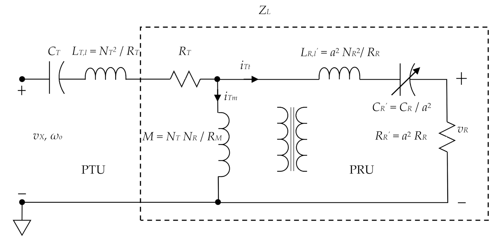
The equivalent circuit of wireless power transfer was shown in Figure 1. The resonant frequency ωo was selected to closely match to reduce the leakage reactance effect on the power transmitting unit (PTU). The power receiving unit (PRU) was used to adjust CR so that the resonance of leakage reactance matched the resonant frequency ωo. Therefore, ωo ≈ ≈ .
The load from the PTU is expressed as follows:
ZL = RT + jωoM ‖ (jωoLR,l’ + 1/(jωoCR’) + RR’)
If all the magnetic flux is transmitted through air with no low reluctance core, then LT,l + M = LT is a constant.
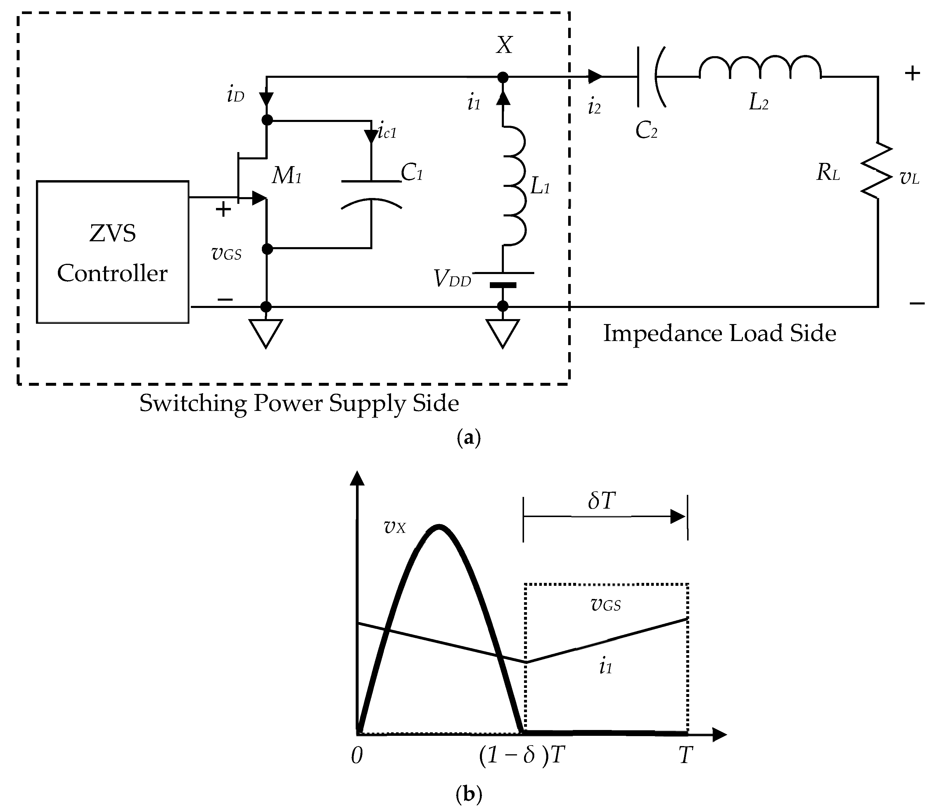
2.2. Class-E Amplifier Circuit Analysis
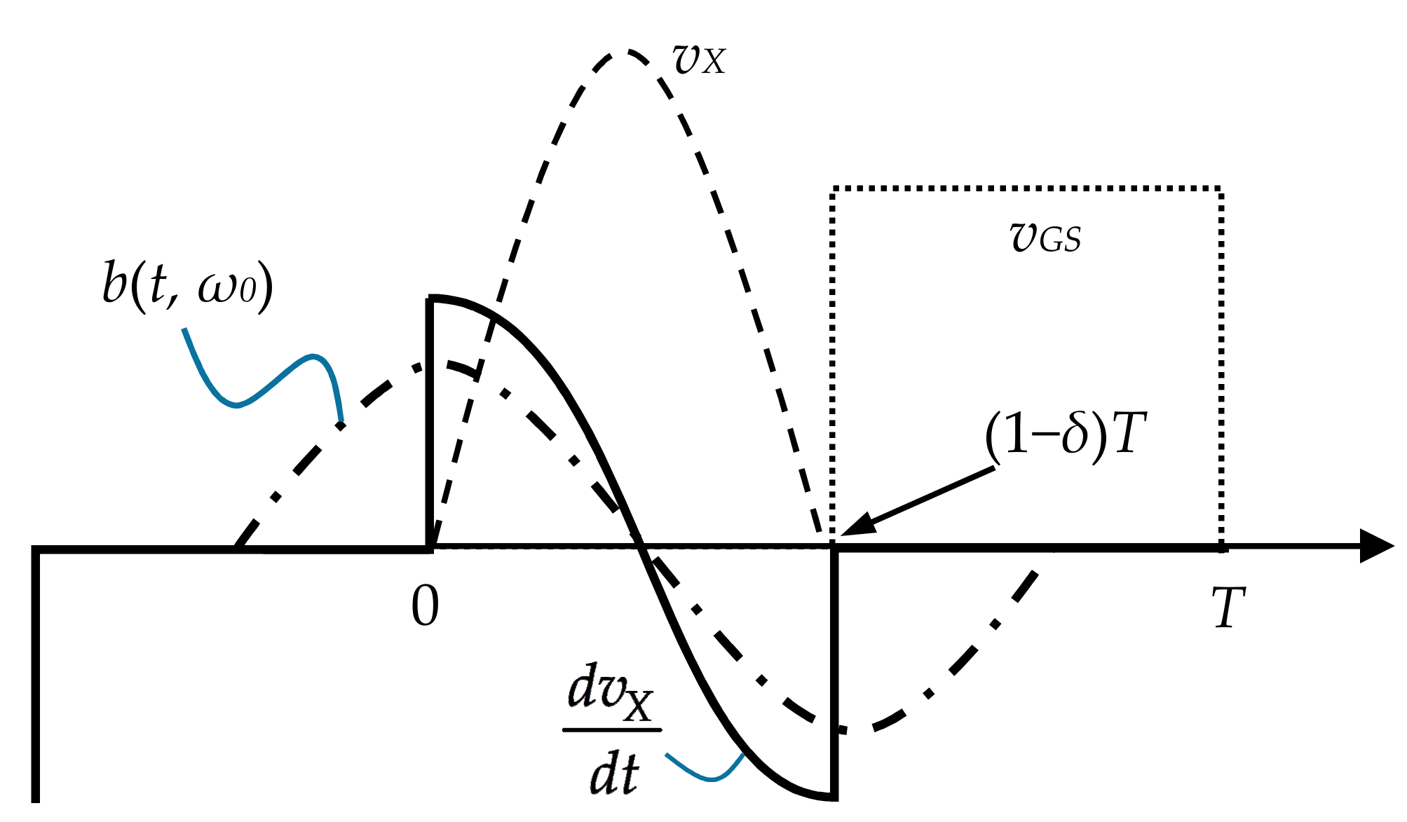
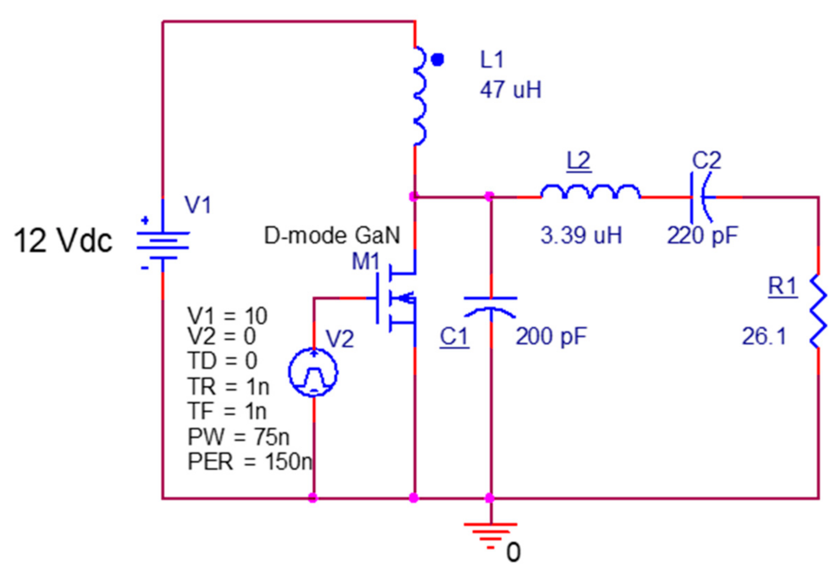
The class-E amplifier (Figure 2a) was used in the PTU to induce the resonance of the output voltage so that the flux density could increase without considerable input power. The actual load ZL for a WPT system is the mutual inductance that is parallel with the equivalent impedance of the receiver side. For simplicity of derivation, we assumed the load to be a purely resistive load and denoted it by RL. The class-E amplifier circuit is divided into the switching power supply and impedance loading. The duty cycle of switching is denoted by δ, and the pulse width is δT (Figure 2b). The conventional power Metal–Oxide–Semiconductor (MOS), Metal–Oxide–Semiconductor Field-Effect Transistor (MOSFET), and Insulated-Gate Bipolar Transistor (IGBT) have body diodes and the negative voltage of vX in the class-E amplifier will be clamped to the body diode threshold. The GaN HEMT transistor has no body diode, thus the voltage vX could be negative and we have to apply the zero current control (ZCS) condition in addition to the ZVS to eliminate this negative voltage situation for better efficiency [3,4].
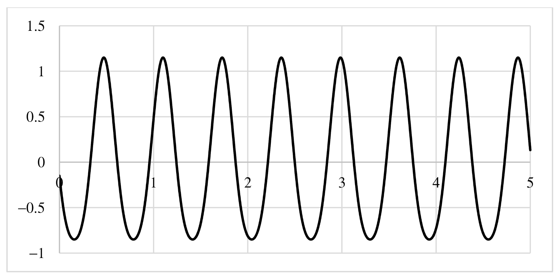
As observed in Figure 3, when the switch is operated at a frequency ωo = 2π/T, the output current is assumed i2 = I2 sin(ωot + β) + I2,a cos(2ωot + β) in steady state. This assumption is made from the observation of experiments. The high order terms I2,a << I2 cause the sinusoidal output to be asymmetrical. Considering β = −180°, I2 = 1, and I2,a = 0.15 as an example, the following assumptions were made to simplify the derivation:
Assumption 1: In the steady state, the output frequency is ωo = 2π/T, and the output current is i2 = I2 sin(ωot + β) + I2,k cos(2kωot + β), as displayed in Figure 3.
2.3. Switching Power Supply Side
For 0 < t < (1 − δ)T, when the transistor is switched off, the inductor current is expressed as follows:
On the basis of previous assumptions, the capacitor voltage can be expressed as follows:
Equation (1) becomes
where
The aforementioned equation may be approximated using the following expression:
The ω3 and are the parameters of input current waveform during the switch-off time derived in [3], and are the most fundamental parameters for the class-E amplifier circuit design. Both the current phase angle and frequency ω3 are functions of the duty ratio which will be derived in the later sequels.
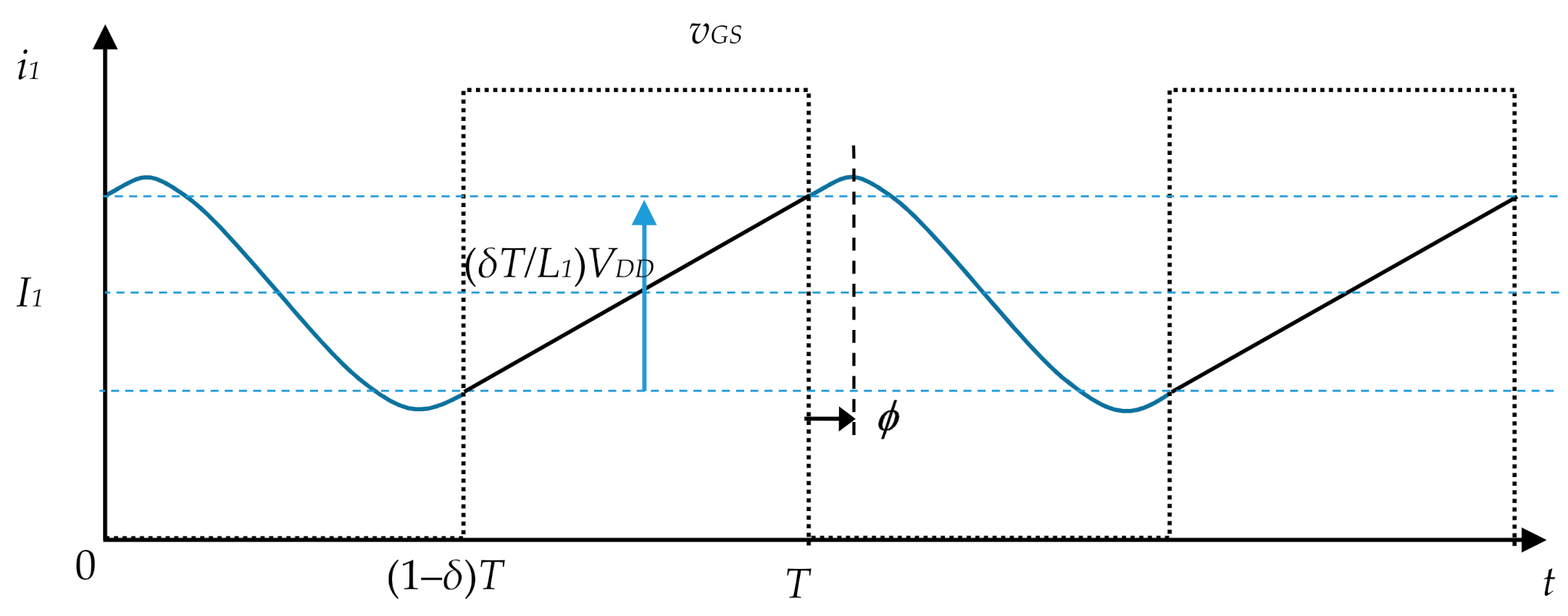
According to Figure 4, the initial conditions of the switch-off time can be calculated from the previous charging time, namely the switch-on time, as follows:
The first derivative of the current i1 must be continuous at the start of the switch-off time. From Equations (6) and (7), we obtain the following expression:
Furthermore:
The boundary condition for the inductor current should also satisfy the following equation:
Therefore,
Assumption 2: (ZVS): vX((1 − δ)T) = 0
The zero-voltage condition of vc1 in which the transistor is turned on again from Equation (2) yields the following equation:
Comparing Equations (9) and (13), we obtained the following equation:
Thus,
Equation (11) yields the following expression:
Combining this equation with Equation (9), we obtained the following expression:
The maximum voltage in the capacitor is derived from dvx(t)/dt = 0 that
Substituting the equation into Equation (12), we obtained the following expression:
and
Table 1 displays the lookup table for some variables versus the duty cycle. The 50% duty cycle is a well-known setting to obtain the nominal switch-voltage waveform [4]. In this paper, we attempt to transcend this conventional setting by varying the duty cycle as shown in Table 1 and not to limit to the 50% duty cycle. As a result, we can achieve better power efficiency for WPT. By adjusting both the duty cycle and resonant frequency, the class-E amplifier can comply with the known phenomenon in GaN HEMT control including the Miller plateau and current clamp [21]. When the maximum voltage in the capacitor is reached, then the following expression is applicable:
that is,
Here, η ≦ 1 is the distortion factor of i2 from the perfect sinusoidal function.
Here, the estimation of I1 in terms of I2,max can be expressed as follows:
Combining Equations (22) and (23), we obtained the following equation:
2.4. Impedance Loading Side
The impedance side has some unknown parameters, namely L2 and RL, to be identified during WPT. In the following derivations, we assumed that they are known.
Due to
We obtain
The input of the aforementioned equation is approximated using the following equation and presented in Figure 5.
The steady-state output current is expressed as follows:
where
Assuming ω0 = ω2 + Δω, , we obtain the following equation:
and
From Equation (22), the maximum voltage in the capacitor VX,max occurs in the middle of the switch-off time. Therefore, we obtain the following expression:
Then, we have the following expression:
which follows that Δω > 0. Thus, ω0 > ω2. Here, we define the proper resonant state, which indicates that Equation (37) is satisfied. The improper resonant state is when Equation (27) fails to hold.
From Equations (22) and (24), we obtain the following equation:
where
Therefore, a successful ZVS must follow that I1 = i2 ((1 − δ)T).
Assumption 3: To ensure proper resonance occurs, ω0 > ω2. Thus, Δω > 0 (see Equation (38)).
Assumption 4: To guarantee a resonance, ω1 << ω0.
Assumption 5: In a proper resonant state, A monotonically increases with the duty cycle δ when the switching frequency ω0 remains constant (see Table 1).
The coefficient η introduced in Equation (22) is the ratio between the input current and the output current. The condition of η = 0.99 implies that the input current is equal to the output current so that there is no other current loss, neither the loss from the power line, the inductor, nor the transistor. Simplified class-E amplifier circuit for the SPICE was shown in Figure 6. In the SPICE analysis, different from the experiment, we had simplified that circuit model, thus the equations used in Table 2 are assuming η = 0.99. Table 2 presents the benchmark of SPICE analyses.
2.5. ZVS Control
Without considerable loss of generality, the capacitor current during the transistor switch-off time is as follows:
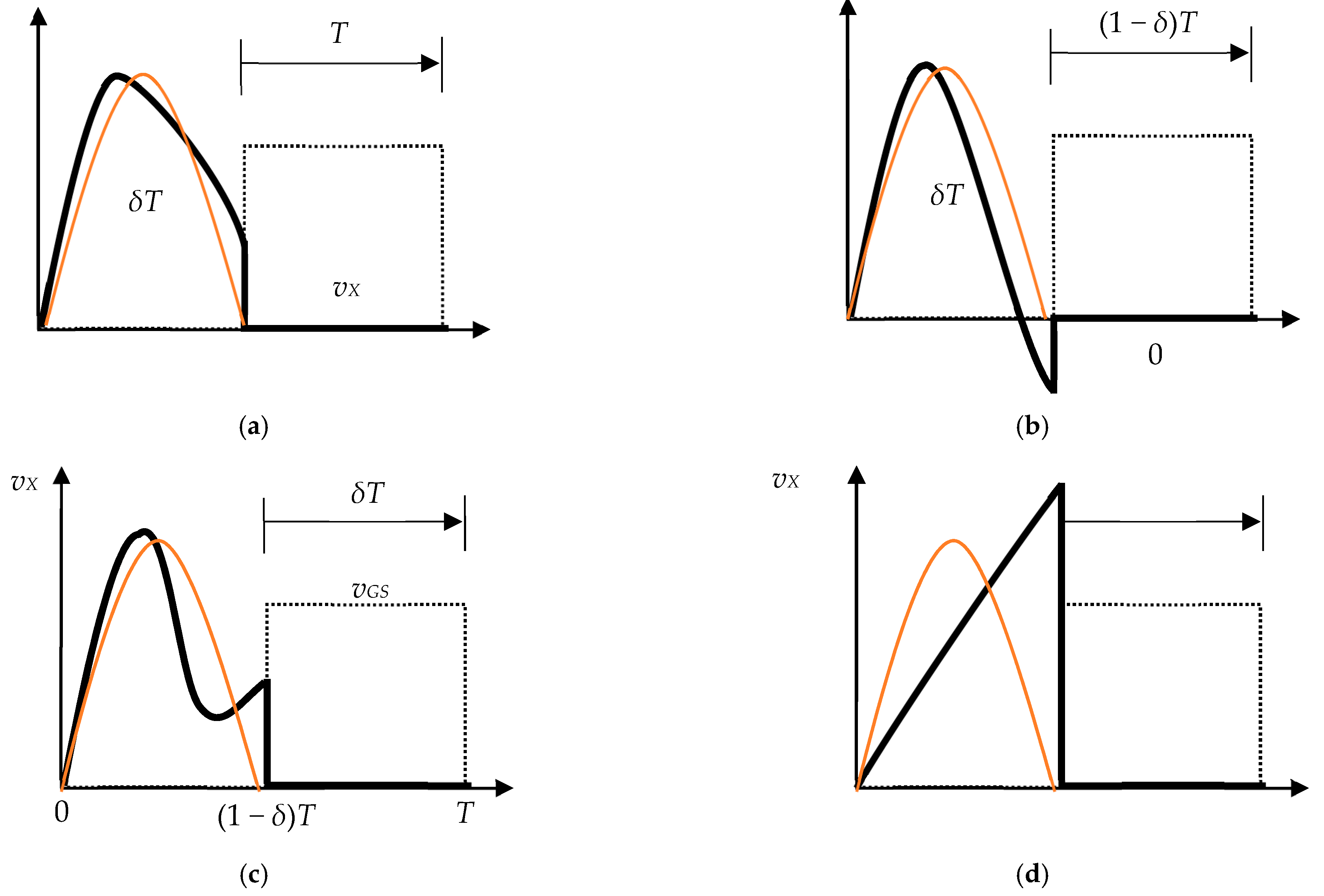
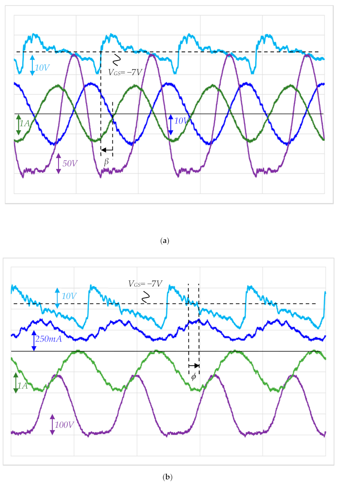
In a proper resonant state, the transistor switch-off time was typically . Thus, the current ripple of the switching power supply inductor A is small. β can affect the capacitor ic1 during the transistor switch-off time more than the current ripple A. In this case, ωo is tuned correctly [∠G2(jωo)]. However, if β is too large, we must decrease δ to obtain a favorable ZVS condition. The result is displayed in Figure 7a. If β is too negative, δ should be increased to obtain appropriate ZVS. The result is displayed in Figure 7b.
When ic1 = 0, the following stationary condition for vX is obtained:
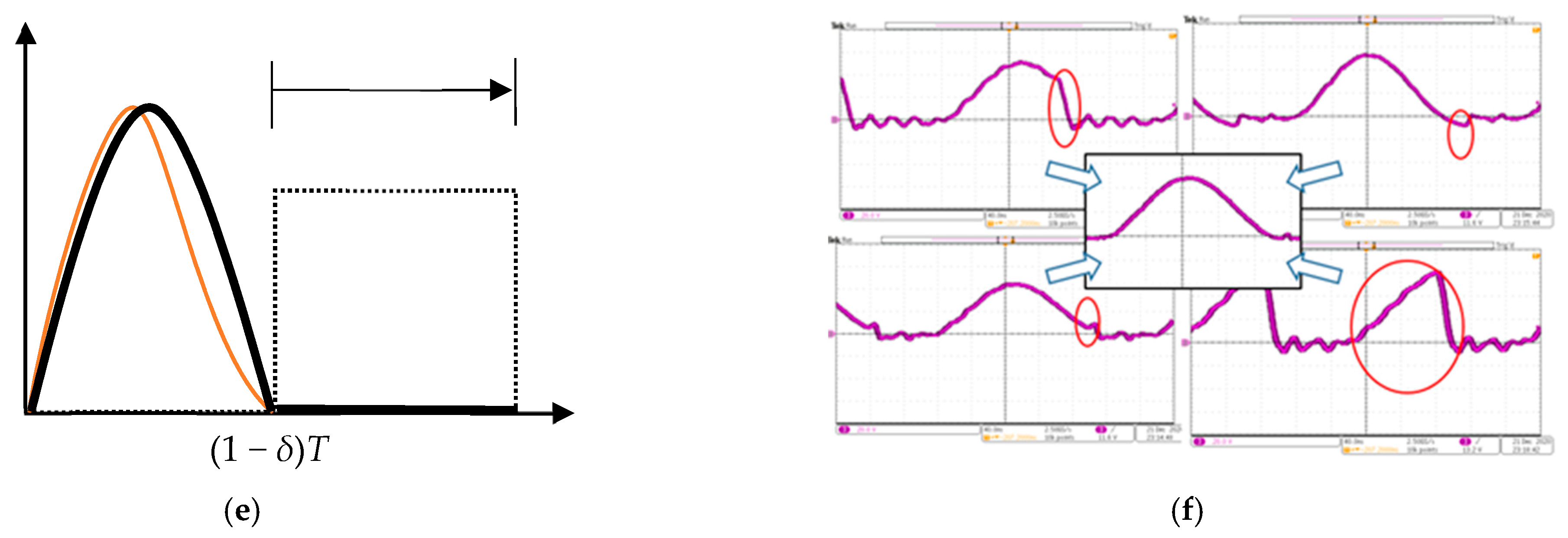
In a proper resonant state, A/I1 << 1 so that A/I1 sin(ω3t + ) + 1 > 0 and sin(ωot + β) = D = sin((1 − δ)π + β) yields the maximum capacitor voltage, which is consistent with the solution in Equation (18). If β is too small, then we may have multiple stationary values during the switch-off time. In this case, β should be increased by adding the switching power supply inductor charging time. Thus, δ should be increased to obtain a satisfactory ZVS. Furthermore, ωo should be increased and the equivalent switch-off time should be reduced to prevent a multiple stationary value situation. The result is displayed in Figure 7c. In other cases, no stationary value exists in the transistor switch-off time, as displayed in Figure 7d. Therefore, ωo should be increased to avoid an improper resonance state.
In a resonant state, at time t = (1 − δ)T for D = sin((1 − δ)π + β), we have the following expression:
The coherence of ZVS and ZCS depend on the current ripple percentage (A/I1%) in the switching power supply inductor. ZCS facilitates smooth turning on of the transistor without disturbing the impedance loading side. The following condition holds for ZCS:
The ZCS condition is provided in Equation (46). In addition, Figure 7b shows an extra ZVS control case with a negative voltage vx other than those found in [4], which needs to satisfy the ZCS condition. Achieving ZCS during ZVS, the resonant frequency ωo could be slightly decreased so that |G2(jωo)| and β increase I1 without affecting ZVS, as displayed in Figure 7e.
The ZVS control depicted in Figure 7a–e is applied to find the best operating condition for resonant frequency and duty cycle, and to control the gate of GaN HEMT. In this research, we used the function generator Tektronix AFG 3104, which is dual channel output equipment that sends 0 to 5V square wave signal to the gate drive [21]. The output of vx is taken from the class-E amplifier to show on the oscilloscope Tektronix MDO 3054. The demo of the ZVS manual operation is shown in Figure 7f.
2.6. D-Mode GaN HEMT
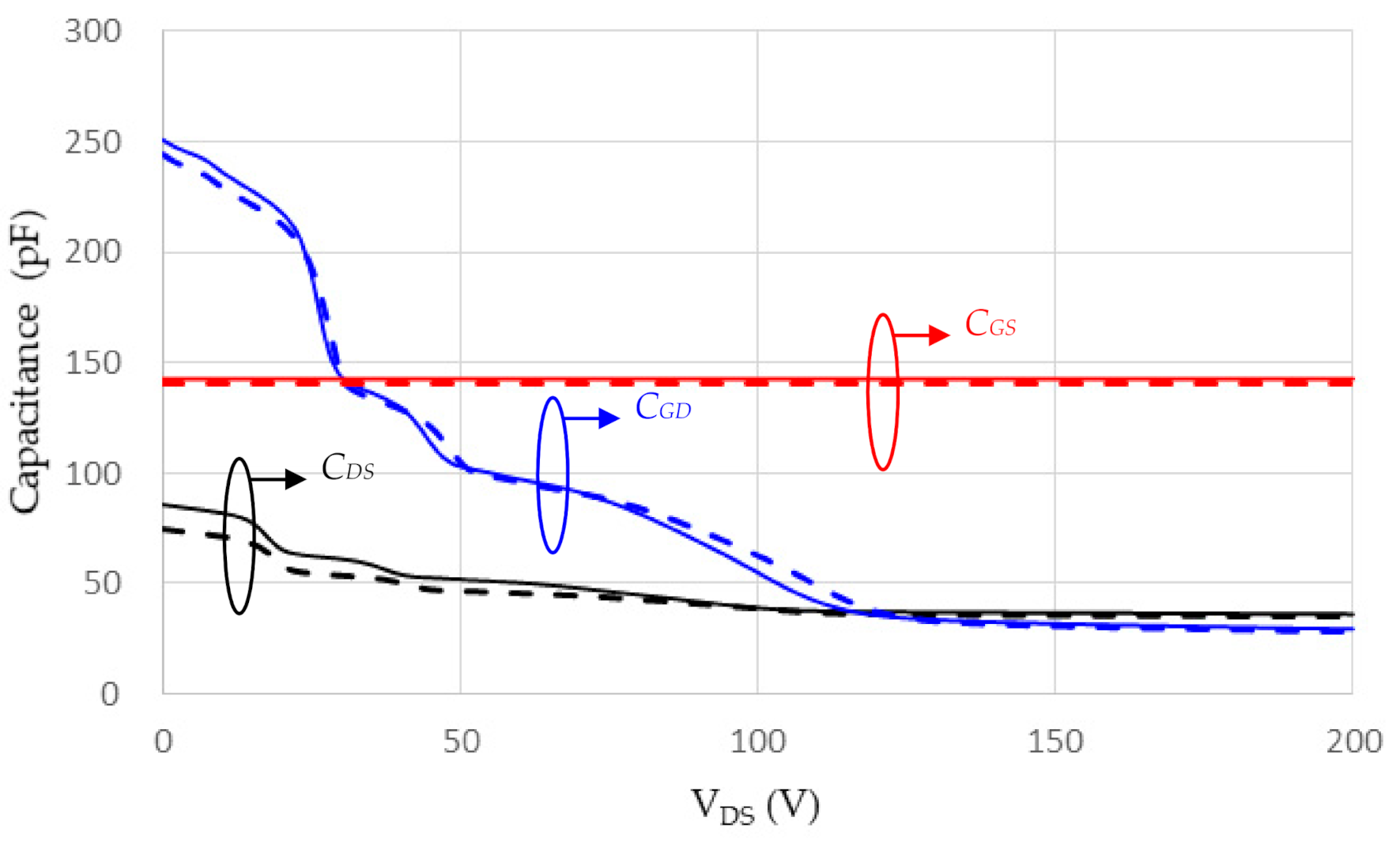
The experiment was based on a D-mode GaN HEMT. The characteristics of the GaN HEMT are displayed in Table 3. A charge pump-type gate drive was applied to switch the GaN HEMT. The parasitic capacitance measurement data are presented in Figure 8. The COSS is the most critical limiting factor for realizing ZVS operation for WPT. Completely eliminating hard switching is difficult for a large increase in COSS at a low drain-source voltage [9]. Here, COSS = CGD + CDS of the D-mode GaN HEMT is only five times that of the low to high drain-source voltages. Furthermore, the capacitances are not sensitive to the switching frequencies in the range 4–5 MHz. Here, CISS = CGD + CGS is three times that of asymmetric effects on the Miller plateau when the transistor is turned on and off.
3. Results
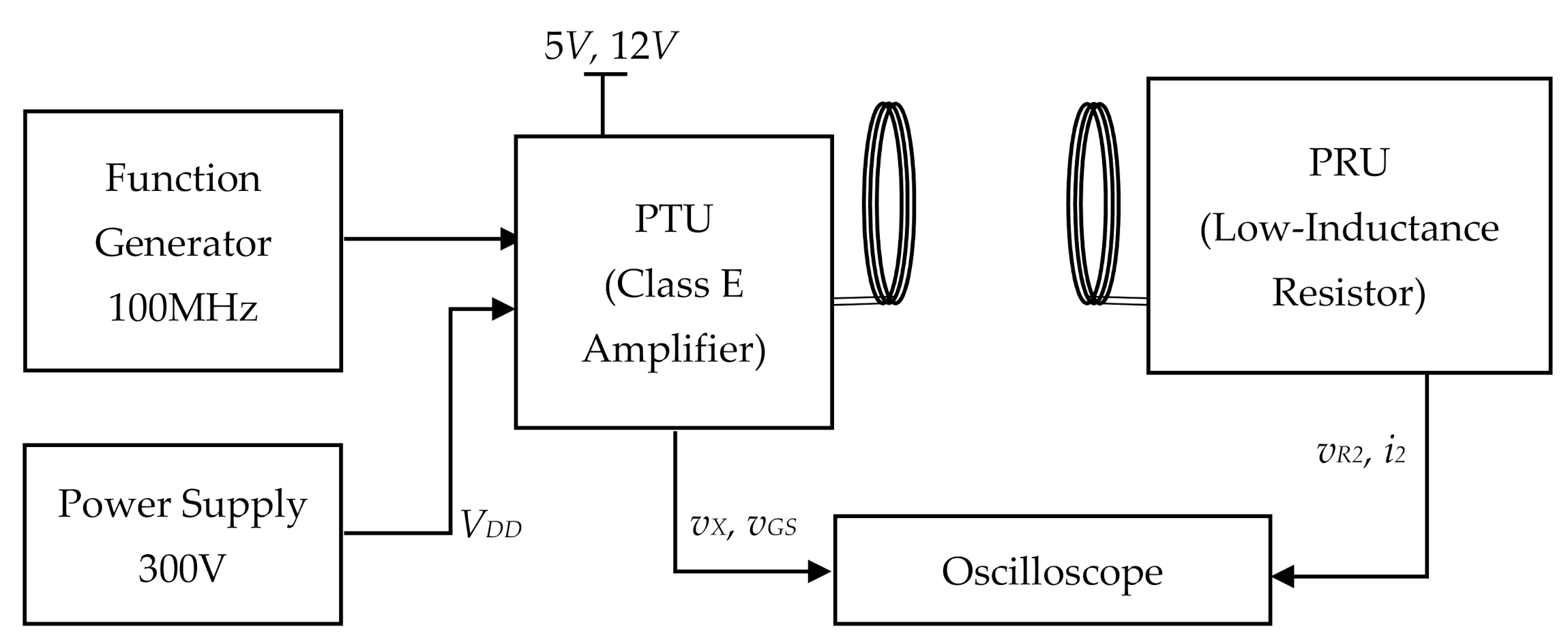
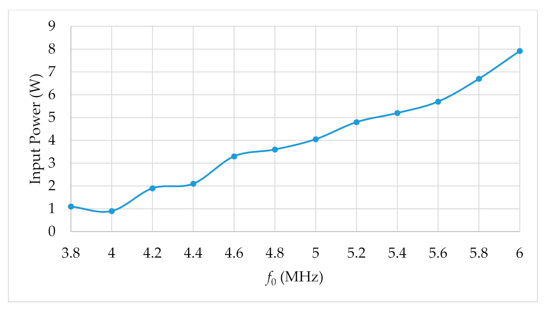
The experimental layout is displayed in Figure 9. The layout consists of a function generator that generates a rectangular pulse train with adjustable frequency and duty cycle in the output. The oscilloscope measures the output current and voltage on the PRU as well as the gate-source voltage and the resonant voltage of the PTU. The oscilloscope (Figure 10a) displays the result when VDD = 110 V such that the i2,PRU (green curve) and vR,PRU (blue curve) of the PRU differ by almost 90° under the resonant WPT condition; the angle β of Equation (33) can be estimated from the value of vGS,ON in Table 3 and the zero current point of i2,PRU. The ZVS control according to Figure 7a–e is applied to manually obtain the drain-source voltage vX (vDS; purple curve). The result is displayed in Figure 10a. Figure 10b reveals the other experiment result of iD,PRU (green curve) and i1 (blue curve) relative to vgs (cyan curve), in which the angle of Equation (17) can be estimated. In the first experiment, we fixed the values of the parameters (Table 4) and measured the input power with no PRU in front of the PTU. Figure 10a and b show two different operating conditions. Table 4 shows only the nominal parameters for the ZVS control used in this research. We have summarized more operating conditions into figures from Figure 11, Figure 12, Figure 13 and Figure 14 to prove the validity of this research. The ZVS control results for various frequencies are displayed in Figure 11. Most of the input power is subjected to the switching loss, which depends on the transistor characteristics, namely the input capacitance CISS = CGD + CGS and also the output capacitance COSS = CGD + CDS. As displayed in Figure 10, the blue curve indicates that the gate-source voltage is not symmetric because of a 30% rectangular gate signal. This is due to the difference in the drain-source voltage at various gate-source voltage states. When the gate is turned on, a successful ZVS occurs on the drain source such that the parasitic capacitor CGD accumulates limited charges. However, a tremendous amount of charge should flow through the gate drive from the ground when the gate turns off because of the high voltage on the drain source when the gate is turned off. The switching loss is the product of the drain current iD and vGS, and almost all of the switching power loss occurs during the gate turning-off time. With the same value of the resonant voltage vX, the higher the switching frequency ωo is, the higher the switching power loss is because it results in a larger ratio of Miller plateau time to the switching time period T. The switching power loss determines the power transfer efficiency. In the experiment displayed in Figure 11, the ZVS control is successful in the range of 3.8–6 MHz. The minimum power loss is at 4.0 MHz when the duty cycle is 30%. Thus, we set the switching frequency to 4.0 MHz for this GaN HEMT for the experiments.
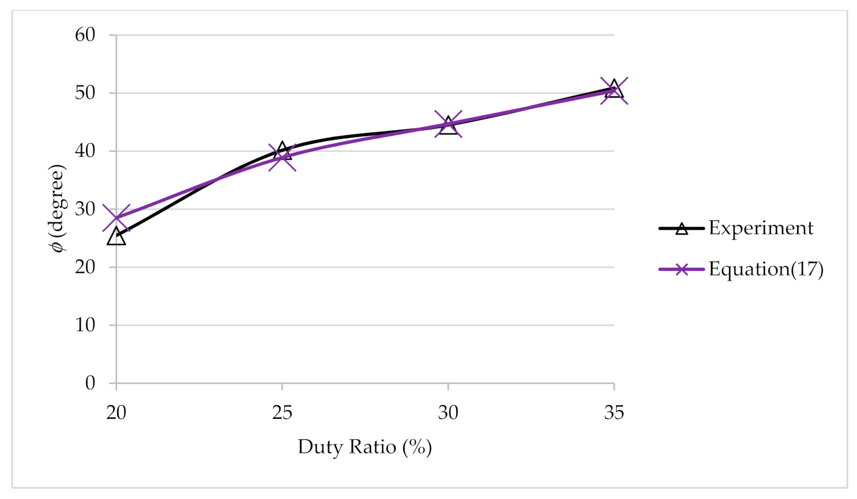
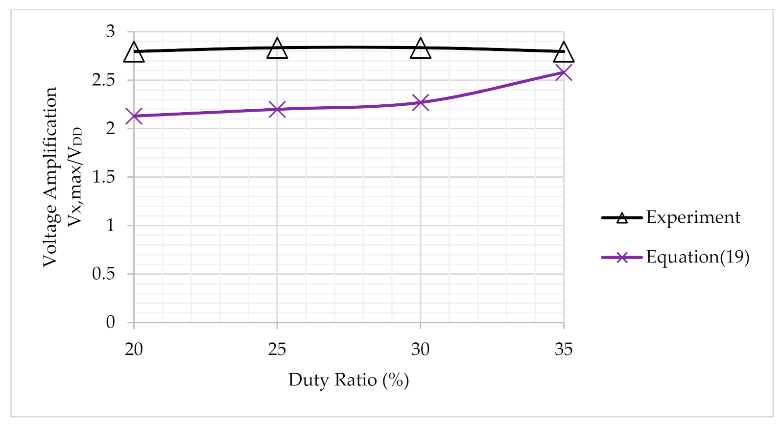
The switching loss is a complex function of the gate-drive parameters, switching frequency, duty cycle, GaN HEMT characteristics, and VDD. We verified the validity of the results in Table 1, which form a basis for ZVS control and a resonant mechanism; a comparison between the results of the experiment and values derived using Equation (17) is presented in Figure 12. The validity of Equation (17) is confirmed even when the switching loss is not included in the derivation. We verified the resonant voltage amplification VX,max/VDD and illustrated the comparison in Figure 13 when the resonant frequency was set to 4.0 MHz. The comparisons indicate that the experiment exhibited slightly higher voltage amplification than the analysis in Equation (19) because the turning-off time of the GaN HEMT was extended. Thus, the equivalent duty ratio percentage in the experiment was higher than the actual input duty ratio percentage. Furthermore, according to Table 1, the voltage amplification VX,max/VDD monotonically increases with an increase in duty ratio. However, the experiment revealed a maximum voltage amplification of approximately 28%. Furthermore, Table 1 provides a guideline for ZVS control.
Power transfer efficiency (PTE (%)) is defined as follows:
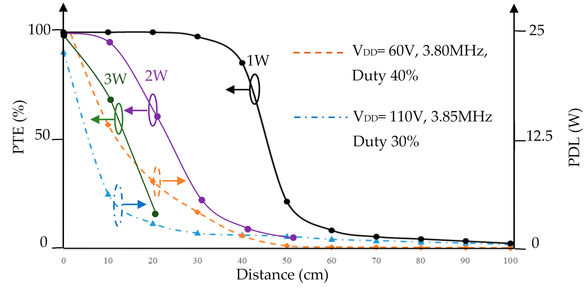
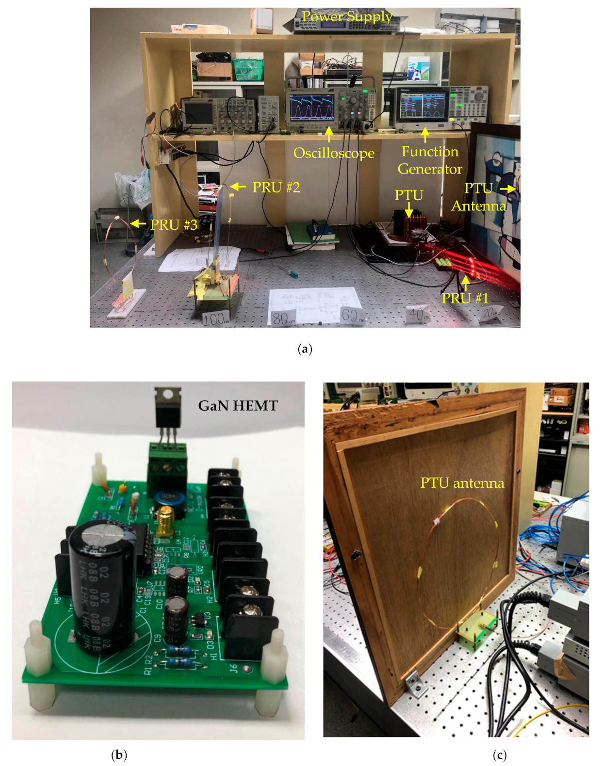
The values of VR,PRU and I2,PRU were obtained from the PRU directly. The experiment was performed with a single PTU, which transferred power to a single PRU. The power loss is calculated from the power difference between the input power sent to the PTU by the power supply CHROMA 62012P-600-8 and the output power measured from the current probe and voltage probe on the PRU taken from the oscilloscope Tektronix MDO3054. The results (Figure 14) revealed that for 1 W of WPT, the efficiency can be as high as 99% when the distance is 20 cm. The PTE (%) can be as high as 80% when the PRU is 40 cm away from PTU. The maximum distance of 1 W power transfer can be as long as 140 cm when VX is ≥700 V, when the corresponding input voltage VDD is around 300 V. The power delivered to load (PDL) is also depicted in Figure 14. It shows that the PDL from a single PTU to a single PRU varies with the distance apart from one another. In order to reach the constant power delivered to the PRU, a closed-loop feedback control mechanism shall be considered [8]; for example, controlling VDD to maintain the constant power is a feasible option. A live photo demonstrating the experiment of multiple PRUs charging is displayed in Figure 15. The design of PTU coils based on Biot–Savart’s law [22] was presented in Appendix A. Multiple PRUs for multiple-input multiple-output (MIMO) wireless power transfer can yield high PTE and the maximum amount of power delivered to the load (PDL) [23,24].
The 99% PTE obtained in our experiment is comparable to the experimental result shown in [16] which uses the coupling tuning-based impedance matching for maximum wireless power transfer efficiency. For 1 W power transfer application, the corresponding I1 on L1 inductor is 20 mA. The class-E amplifier in this paper uses only one GaN HEMT transistor with no body diode, thus no rectifier loss. The GaN HEMT with 100 mΩ RD,on loss is less than 0.1% of the total power input. The switching loss under the zero-voltage switching condition is also less than 1 mW. The high-frequency inductor L1 coil loss is 0.2 mW loss. The coil loss of L2 is a function of distance, which is not directly measurable, therefore Equation (47) is used instead to calculate the PTE. The systematic procedure for WPT design is shown in Figure 16. Following the systematic design procedure, the comparison through analyses, simulations, and experiments can be verified and the operating conditions can be adjusted according to the best power efficiency for various applications.
4. Conclusions
The resonance mechanism of the 6.78 MHz resonant WPT was analyzed. The D-mode GaN HEMT with no body diode can prevent the current leakage from C1 and enhance the voltage resonance. The ZVS control was derived in terms of the resonant frequency and duty cycle. The experiments agreed with the derivation of the ZVS control. For 1 W of WPT, the efficiency can be as high as 99% when the transfer distance is within 20 cm. The PTE can be as high as 80% when the PRU is 40 cm. The maximum distance of 1 W power transfer can be 140 cm when VX is ≥ 700 V. The GaN HEMT made in National Chiao Tung University (NCTU) has a breakdown voltage higher than 1000 V. The critical problem for the WPT is the switching loss of the GaN HEMT transistor. In the future, a detailed SPICE circuit analysis of the class-E amplifier should also consolidate the precise GaN HEMT transistor model and its gate-drive circuit to improve the power efficiency. In order to reach a constant PDL while the distance of the PRU is varying, the VDD may follow the corresponding distance change. In the closed control loop, the required feedback of the actual power reading of the PRU via a 2.4 GHz communication network is recommended by the Airfuel Alliance.
References
Author Contributions
Conceptualization, E.Y.C. and W.-H.C.; methodology, C.-Y.L., G.-B.W.; software, C.-C.W.; validation, C.-Y.L., G.-B.W., C.-C.W.; formal analysis, S.C.; resources, S.C.; writing—original draft preparation, W.-H.C.; writing—review and editing, C.-C.W.; visualization, E.Y.C.; supervision, E.Y.C.; project administration, E.Y.C.; funding acquisition, W.-H.C. All authors have read and agreed to the published version of the manuscript.
Funding
This research was funded by Ministry of Science and Technology, R.O.C., grant number MOST(NSC)109-3116-F009-001-CC1.
Institutional Review Board Statement
Not applicable.
Informed Consent Statement
Not applicable.
Data Availability Statement
Data sharing is not applicable.
Acknowledgments
This work was supported by Ministry of Science and Technology, R.O.C. The authors would also like to thank You-Chen Weng in CSD Lab for providing the fabrication of D-Mode MIS-HEMT chips, and IM Lab graduate students Yue-Cong Sie and Professor Li-Chuan Tang for their help in the experiment setup.
Conflicts of Interest
The authors declare no conflict of interest.
Nomenclature
| Symbol | Abbreviation |
|---|---|
| RT | reluctance of the leakage flux on the power transmitting unit (PTU) side |
| RR | reluctance of the leakage flux on the power receiving unit (PRU) side |
| RM | reluctance of the mutual flux link on both PTU and PRU sides |
| NT | number of turns of antenna on PTU side |
| NR | number of turns of antenna on PRU side |
| a | NT/NR is the turn ratio |
| ωo | frequency adopted in wireless power transfer |
| L1 | inductance on the switching power supply side of the PTU |
| C1 | resonant capacitance on the switching power supply side of the PTU |
| L2 | inductance on the impedance load side of the PTU |
| C2 | resonant capacitance on the impedance load side of the PTU |
| RL | equivalent load of PRU on the PTU side |
| T | switching period time ωo = 2π / T |
| M | mutual inductance of the WPT |
| LT,l | leakage inductance of the PTU |
| LT | total inductance of the PTU |
| LR,l | leakage inductance of the PRU |
| LR | total inductance of the PRU |
| ω1 | natural frequency of the LC tank in the PTU |
| ω2 | output current frequency |
| ω3 | input current frequency during the switch-off time |
| φ | input current phase angle during the switch-off time |
Appendix A. PTU Coil Specifications
Theoretically, the inductance of circular loops may be as though the magnetic field is everywhere in the interior plane of a single circular loop of wire carrying current I, where the loop has radius R = D/2 and the wire has radius a. According to Figure A1, we put the origin at the center of the loop and let the z-axis point normal to the plane of the loop. We can also orient the x-axis so that the point at which we want to find the magnetic field is located at coordinates 0 x < R − a, y = 0, and z = 0 as sketched below.
Figure A1.
The coil dimension.

The following equation is obtained based on Biot–Savart’s law [22].
On the other hand, the inductance can also be derived from Faraday’s law that
From an experiment using the RLC meter GWINSTEK LCR819, we measured three inductors using the AWG22 copper wire whose wire diameter was 0.643 mm with different arrangements. The result is shown in Table A1.

Table A1.
Measured three inductors with different arrangements.
| N (turns) | D (cm) | L (uH) |
|---|---|---|
| 3 | 33.5 | 10.5 |
| 4 | 19 | 8.6 |
| 21 | 8.5 | 46 |
The coefficient is calculated using
Comparing Equation (A1) with Equation (A2), we have
Figure A2 shows the comparison between the result from empirical Equation (A3) and that from theoretical Equation (A4). The result shows that the theoretical equation can only be valid for a range between 20 cm and 30 cm in the wireless power transfer application with flat coils. (A2) substituted with Equation (A3) is adopted in this paper for the coil design.
Figure A2.
Comparison between theoretical result and the experiments.

Two sets of PTU/PRU inductors are used in the experiments; we measured the parameters of the coils on the GW/Instek LCR-819 100 KHz LCR Meter and calculated the self-resonant frequency (SRF) for individual coils. The data are provided in Table A2.
Table A2.
Coil specifications used in the WPT experiments in this paper.
| Inductor ID | Inductance (uH) | Capacitance (pF) | Resistor (Ohm) | Q Factor | SRF (MHz) |
|---|---|---|---|---|---|
| Tx1 | 8.87 | 28.54 | 0.128 | 4.364 | 10.00 |
| Tx2 | 8.88 | 28.53 | 0.128 | 4.342 | 9.99 |
| Rx1 | 9.03 | 27.7 | 0.081 | 7.06 | 10.06 |
| Rx2 | 9.05 | 27.9 | 0.074 | 7.66 | 10.02 |
References
- Zhang, Z.; Pang, H.; Georgiadis, A.; Cecati, C. Wireless power transfer—An overview. IEEE Trans. Ind. Electron. 2018, 66, 1044–1058. [Google Scholar]
- Huynh, P.S.; Ronanki, D.; Vincent, D.; Williamson, S.S. Overview and Comparative Assessment of Single-Phase Power Converter Topologies of Inductive Wireless Charging Systems. Energies 2020, 13, 2150. [Google Scholar]
- Sokal, N.O.; Sokal, A.D. Class E—A new class of high-efficiency tuned single-ended switching power amplifiers. IEEE J. Solid-State Circuits 1975, 10, 168–176. [Google Scholar]
- Sokal, N.O. Class-E RF power amplifiers. Qex Commun. Quart. 2001, 204, 9–20. [Google Scholar]
- Arteaga, J.M.; Aldhaher, S.; Kkelis, G.; Kwan, C.; Yates, D.C.; Mitcheson, P.D. Dynamic capabilities of multi-MHz inductive power transfer systems demonstrated with batteryless drones. IEEE Trans. Power Electron. 2018, 34, 5093–5104. [Google Scholar]
- Dai, W.; Tang, W.; Cai, C.; Deng, L.; Zhang, X. Wireless power charger based on class E amplifier with the maximum power point load consideration. Energies 2018, 11, 2378. [Google Scholar]
- Wen, F.; Cheng, X.; Li, Q.; Ye, J. Wireless Charging System Using Resonant Inductor in Class E Power Amplifier for Electronics and Sensors. Sensors 2020, 20, 2801. [Google Scholar]
- Green, P.B. Class-E Power Amplifier Design for Wireless Power Transfer. August 2018. Rev 1.2. Infineon, Appl. Note 1803. pp. 1–51. Available online: https://www.infineon.com/wirelesscharging (accessed on 10 August 2018).
- Christ, A.; Douglas, M.; Nadakuduti, J.; Kuster, N. Assessing Human Exposure to Electromagnetic Fields from Wireless Power Transmission Systems. Proc. IEEE 2013, 101, 1482–1493. [Google Scholar]
- Paolucci, M.; Green, P.B. Benefits of GaN e-Mode HEMTs in Wireless Power Transfer—GaN Power Devices in Resonant Class D and Class E Radio Frequency Power Amplifiers. October 2018. Rev 1.0. Infineon, White Paper. Available online: https://www.infineon.com/wirelesscharging (accessed on 17 October 2018).
- Stephan, S.; Matthias, B. Resonant Wireless Power Transfer, Infineon, White Paper. Available online: www.infineon.com/wirelesscharging (accessed on 29 May 2018).
- Pinuela, M.; Yates, D.C.; Lucyszyn, S.; Mitcheson, P.D. Maximizing DC-to-load efficiency for inductive power transfer. IEEE Trans. Power Electron. 2013, 28, 2437–2447. [Google Scholar]
- Aldhaher, S.; Luk, P.C.K.; Whidborne, J.F. Tuning class E inverters applied in inductive links using saturable reactors. IEEE Trans. Power Electron. 2013, 29, 2969–2978. [Google Scholar]
- Aldhaher, S.; Luk, P.C.K.; Bati, A.; Whidborne, J.F. Wireless power transfer using Class E inverter with saturable DC-feed inductor. IEEE Trans. Ind. Appl. 2014, 50, 2710–2718. [Google Scholar]
- Porto, R.W.; Brusamarello, V.J.; Pereira, L.A.; de Sousa, F.R. Fine tuning of an inductive link through a voltage-controlled capacitance. IEEE Trans. Power Electron. 2016, 32, 4115–4124. [Google Scholar]
- Barman, S.D.; Reza, A.W.; Kumar, N. Coupling Tuning Based Impedance Matching for Maximum Wireless Power Transfer Efficiency. J. Comput. Sci. Comput. Math. 2016, 6, 91–96. [Google Scholar]
- Fu, M.; Yin, H.; Liu, M.; Ma, C. Loading and power control for a high-efficiency class E PA-driven megahertz WPT system. IEEE Trans. Ind. Electron. 2016, 63, 6867–6876. [Google Scholar]
- Zhang, S.; Zhao, J.; Wu, Y.; Mao, L.; Xu, J.; Chen, J. Analysis and Implementation of Inverter Wide-Range Soft Switching in WPT System Based on Class E Inverter. Energies 2020, 13, 5187. [Google Scholar]
- Hayati, M.; Roshani, S.; Kazimierczuk, M.K.; Sekiya, H. Analysis and design of class E power amplifier considering MOSFET parasitic input and output capacitances. IET Circuitsdevices Syst. 2016, 10, 433–440. [Google Scholar]
- Wen, F.; Li, R. Parameter Analysis and Optimization of Class-E Power Amplifier Used in Wireless Power Transfer System. Energies 2019, 12, 3240. [Google Scholar]
- Weng, Y.C.; Wu, C.C.; Edward, C.Y.; Chieng, W.H. Minimum Power Input Control for Class-E Amplifier Using Depletion-Mode Gallium Nitride High Electron Mobility Transistor. Energies. plan to resubmit.
- Edward, B.R.; Louis, C. On the Self-Inductance of Circles, U.S. Department of Commerce and Labor, Bureau of Standards; University of Michigan: Michigan, MI, USA, 1907; pp. 149–159. [Google Scholar]
- Kim, J.W.; Son, H.C.; Kim, K.H.; Park, Y.J. Efficiency Analysis of Magnetic Resonance Wireless Power Transfer with Intermediate Resonant Coil. IEEE Antennas Wirel. Propag. Lett. 2011, 10, 389–392. [Google Scholar]
- Ahn, D.; Hong, S. Effect of Coupling between Multiple Transmitters or Multiple Receivers on Wireless Power Transfer. IEEE Trans. Ind. Electron. 2013, 60, 2602–2613. [Google Scholar]
Figure 1.
Wireless power transfer equivalent circuit.

Figure 2.
(a) Class-E amplifier of the PTU; (b) Pulse Width Modulation (PWM) control of D-mode GaN HEMT.
Figure 2.
(a) Class-E amplifier of the PTU; (b) Pulse Width Modulation (PWM) control of D-mode GaN HEMT.

Figure 3.
Output current (i2) waveform of the class-E amplifier.

Figure 4.
Input current (i1) of the switching power supply side of the class-E amplifier.

Figure 5.
Excitation function to the impedance load side of the class-E amplifier.

Figure 6.
Simplified class-E amplifier circuit for the Simulation Program with Integrated Circuit Emphasis (SPICE) analysis.
Figure 6.
Simplified class-E amplifier circuit for the Simulation Program with Integrated Circuit Emphasis (SPICE) analysis.

Figure 7.
(a) ωo should be fixed and δ should be decreased; (b) ωo should be fixed and δ should be increased; (c) both ωo and δ should be increased; (d) ωo should be increased and δ should be fixed; (e) slightly decrease ωo and fix δ for ZCS; (f) the experiment correspondences.
Figure 7.
(a) ωo should be fixed and δ should be decreased; (b) ωo should be fixed and δ should be increased; (c) both ωo and δ should be increased; (d) ωo should be increased and δ should be fixed; (e) slightly decrease ωo and fix δ for ZCS; (f) the experiment correspondences.


Figure 8.
Parasitic capacitance measurement of the D-mode GaN HEMT. CGS (red curve), CGD (blue curve), CDS (black curve), parasitic capacitance under 5 MHz (solid line), under 4 MHz (dashed line).
Figure 8.
Parasitic capacitance measurement of the D-mode GaN HEMT. CGS (red curve), CGD (blue curve), CDS (black curve), parasitic capacitance under 5 MHz (solid line), under 4 MHz (dashed line).

Figure 9.
Experiment layout with a single PTU transferring power to multiple PRUs. The PTU antenna is hidden behind the painting shown in Figure 9.
Figure 9.
Experiment layout with a single PTU transferring power to multiple PRUs. The PTU antenna is hidden behind the painting shown in Figure 9.

Figure 10.
(a) Oscilloscope screen dump showing i2,PRU (green curve), vDS (purple curve), vR,PRU (blue curve), and vgs (cyan curve). (b) Oscilloscope screen dump showing iD,PRU (green curve), i1 (blue curve), and vgs (cyan curve).
Figure 10.
(a) Oscilloscope screen dump showing i2,PRU (green curve), vDS (purple curve), vR,PRU (blue curve), and vgs (cyan curve). (b) Oscilloscope screen dump showing iD,PRU (green curve), i1 (blue curve), and vgs (cyan curve).

Figure 11.
Input power versus resonant frequency.

Figure 12.
Comparison between experimental values and those obtained using Equation (17).

Figure 13.
Comparison between the experiment and Equation (19).

Figure 14.
Power transfer efficiency and PDL versus the distance between PTU and PRU.

Figure 15.
Live example of WPT to multiple PRUs. (a) Experiment setup with a single PTU transferring power to multiple PRUs. The PTU antenna is hidden behind the painting. The layout is shown in Figure 15; (b) the close picture of class-E PA, and (c) the close picture of PTU antenna.
Figure 15.
Live example of WPT to multiple PRUs. (a) Experiment setup with a single PTU transferring power to multiple PRUs. The PTU antenna is hidden behind the painting. The layout is shown in Figure 15; (b) the close picture of class-E PA, and (c) the close picture of PTU antenna.

Figure 16.
Flowchart of a systematic procedure for WPT design.

Table 1.
Lookup table for various parameters versus the duty cycle.
| δ | φ (Degree) | ||||
|---|---|---|---|---|---|
| 10% | 16 | 0.91 | 1.01 | 2.04 | 1.03 |
| 20% | 28.5 | 0.84 | 1.05 | 2.13 | 1.08 |
| 30% | 38 | 0.79 | 1.12 | 2.27 | 1.12 |
| 40% | 55.3 | 0.69 | 1.15 | 2.75 | 1.53 |
| 50% 1 | 64 | 0.64 | 1.3 | 3.28 | 1.78 |
| 60% | 71 | 0.61 | 1.5 | 4.07 | 2.01 |
| 70% | 76.5 | 0.58 | 1.9 | 5.28 | 2.22 |
| 80% | 81.5 | 0.55 | 2.7 | 7.67 | 2.46 |
| 90% | 86 | 0.52 | 5.2 | 15.33 | 2.76 |
1 Reference [4].
Table 2.
Benchmark between equations and the SPICE result with η = 0.99.
| Equation | Symbol | Unit | Analysis Result | SPICE Result | Error (%) |
|---|---|---|---|---|---|
| RL | Ω | 26 | |||
| C1 | pF | 200 | |||
| C2 | pF | 220 | |||
| L1 | uH | 47 | |||
| L2 | uH | 3.4 | |||
| ω1/2π | MHz | 2.32 | |||
| ω0/2π | MHz | 6.66 | |||
| T | ns | 150 | |||
| ω2/2π | MHz | 5.8 | |||
| Δω/2π | MHz | 0.866 | |||
| δ | 0.5 | ||||
| (17) | degree | 64 | 63 | 1% | |
| (15) | ω3/2π | MHz | 8.65 | 8.5 | 2% |
| (19) | VX,max | V | 39.36 | 42 | 6% |
| (20) | A | mA | 10.8 | 10 | 8% |
| (32) | β | degree | −53 | −55 | 2% |
| (24) | I2,max | A | ±553 | 0.5/−0.421 | 10% |
| (30) | B | mA | 219 | 239 | 8% |
| (22) | I1 | mA | 332 | 235 | 35% |
Table 3.
Characteristic summary of the D-mode GaN HEMT.
| Symbol | Parameter | Value | Unit |
|---|---|---|---|
| vGS,ON | Turn-on voltage | −7 | V |
| CDS | Drain-source parasitic capacitance | 75 | pF |
| CGD | Gate-drain Parasitic capacitance | 245 | pF |
| CGS | Gate-source Parasitic capacitance | 140 | pF |
| VGS,max | Maximum gate-source voltage | 8 | V |
| VDS,BD | Drain-source breakdown voltage | 1000 | V |
| id,max | Maximum drain current | 35 | A |
Table 4.
Nominal parameters for ZVS control.
| Symbol | Value | Unit |
|---|---|---|
| RL,2 (PRU) | 50 | Ω |
| C1 | 320 | pF |
| C2 | 100 | pF |
| L1 | 47 | µH |
| L2 | 8 | µH |
| δ | 30 % | - |
| VDD | 36 | V |
Publisher’s Note: MDPI stays neutral with regard to jurisdictional claims in published maps and institutional affiliations. |
© 2021 by the authors. Licensee MDPI, Basel, Switzerland. This article is an open access article distributed under the terms and conditions of the Creative Commons Attribution (CC BY) license (http://creativecommons.org/licenses/by/4.0/).
Share and Cite
MDPI and ACS Style
Liu, C.-Y.; Wang, G.-B.; Wu, C.-C.; Chang, E.Y.; Cheng, S.; Chieng, W.-H. Derivation of the Resonance Mechanism for Wireless Power Transfer Using Class-E Amplifier. Energies 2021, 14, 632. https://0-doi-org.brum.beds.ac.uk/10.3390/en14030632
AMA Style
Liu C-Y, Wang G-B, Wu C-C, Chang EY, Cheng S, Chieng W-H. Derivation of the Resonance Mechanism for Wireless Power Transfer Using Class-E Amplifier. Energies. 2021; 14(3):632. https://0-doi-org.brum.beds.ac.uk/10.3390/en14030632
Chicago/Turabian StyleLiu, Ching-Yao, Guo-Bin Wang, Chih-Chiang Wu, Edward Yi Chang, Stone Cheng, and Wei-Hua Chieng. 2021. "Derivation of the Resonance Mechanism for Wireless Power Transfer Using Class-E Amplifier" Energies 14, no. 3: 632. https://0-doi-org.brum.beds.ac.uk/10.3390/en14030632
Note that from the first issue of 2016, this journal uses article numbers instead of page numbers. See further details here.