
A Physics-Based Analytical Model for Current–Voltage Characteristics of Perovskite Solar Cells Incorporating Bulk Recombination


Department of Electrical and Computer Engineering, Concordia University, 1455 Blvd. de Maisonneuve West, Montreal, QC H3G 1M8, Canada
Energies 2021, 14(13), 3868; https://0-doi-org.brum.beds.ac.uk/10.3390/en14133868
Submission received: 27 May 2021
/
Revised: 18 June 2021
/
Accepted: 24 June 2021
/
Published: 27 June 2021
(This article belongs to the Special Issue Nano-Structured Solar Cells 2020-2022)
Abstract
:A physics-based compact analytical model for studying the current–voltage characteristics of perovskite solar cells has been proposed by considering the external voltage-dependent carrier transport, exponential photon absorption, and bulk charge carrier recombination. The explicit analytical expressions for both the forward dark and photocurrents in perovskite solar cells are derived. The current in the external circuit is calculated considering the actual solar spectrum. The mathematical models are verified and useful physical parameters are extracted by comparing the model calculations with the published experimental results on various perovskite solar cells. The proposed model shows excellent agreement with the experimental results. The power conversion efficiency can be improved further by enhancing the carrier transport in the perovskite layer. The improvement in charge carrier transport enhances the fill factor and hence the power conversion efficiency.
1. Introduction
Halide perovskite solar cells (PSCs) have attracted widespread attention in recent years due to their high power conversion efficiency and solution-based easy fabrication [1,2]. The power conversion efficiency (PCE) of these PSCs has reached above 20% within only 5 years of research and development [3,4]. To date, the following three perovskite halides have shown very promising photovoltaic characteristics: (i) methylammonium lead triiodide (MAPbI3, where MA is CH3NH3), (ii) mixed halide MAPbI3−xClx, and (iii) formamidinium-based (FAPbI3)0.85 (MAPbBr3)0.15, where FA is NH2CHNH2. Among these perovskites, MAPbI3 is the most studied material [5,6]. The reported bandgap of MAPbI3 is 1.55–1.6 eV. Cl doping to MAPbI3 improves the stability of the perovskite film and thus MAPbI3−xClx is commercially more stable. The bandgap of MAPbI3−xClx is 1.55 eV and it shows light absorption at a wavelength of up to 790 nm [1]. The bandgap of FAPbI3 is 1.47 eV. FAPbI3 shows broader light absorption of the solar spectrum than MAPbI3. However, FAPbI3 is less stable than MAPbI3. The perovskite (FAPbI3)0.85 (MAPbBr3)0.15 shows a stable perovskite phase, having a bandgap of 1.55 eV, and absorbs light at a wavelength of up to 840 nm. The optical gap is slightly lower (~40 meV) than the fundamental electronic bandgap [7].
The above polycrystalline perovskites show good carrier transport properties. The electron and hole mobilities are in the range of 2–10 and 5–15 cm2V−1s−1, respectively [8,9]. Although some of the perovskite solar cells exhibit visible hysteresis in the current–voltage (J-V) characteristics under forward and reverse bias sweep [10], this hysteresis behavior depends on the perovskite materials (FAPbI3 or MAPbI3) and cell architecture (n-i-p or p-i-n) [2,3]. For example, the ITO/PEDOT:PSS/MAPbI3/PCBM/Ag or ITO/PCBM/MAPbI3/TaTm/Au solar cell structure shows negligible hysteresis [10,11]. In these two structures, PEDOT:PSS or TaTm is the hole transport layer (HTL) and PCBM is the electron transport layer (ETL). FAPbI3-based PSCs with a n-i-p architecture show insignificant hysteresis [2]. FAPbI3-based perovskite solar cells show a state-of-the-art power conversion efficiency of 20.8% [3]. Though PSCs show high PCE in a small area, their efficiency degrades in large-area cells [12]. Therefore, it is vital to understand the physics of device operation to identify the factors that limit their efficiency and determine methods to improve their performance further. In this context, a physics-based model for the voltage-dependent photo- and dark currents is vital for improving the required areas of material properties and device structure.
A limited number of attempts have been made in the literature to model the current–voltage characteristics of perovskite solar cells [13,14]. Richardson et al. [13] described extensively the hysteresis phenomenon in perovskite solar cells by considering the motion of ions. Sherker et al. [14] proposed a drift-diffusion model by numerically solving the continuity and Poisson’s equations. They did not show the physics of the dark current, and the model fitting showed a significant deviation from the experimental results. Sun et al. [15] developed an analytical model for perovskite solar cells but their model did not consider bulk carrier recombination. The bulk recombination has a significant effect on both the dark and photocurrents.
The photogenerated electrons and holes drift across the perovskite layer by the built-in electric field and some of these carriers are lost by bulk recombination. The large dielectric constant of perovskite materials screens the presence of electrons and holes, which results in a very low bimolecular recombination coefficient in perovskites [16]. The polycrystalline perovskite is close to an intrinsic semiconductor [16]. The dominant recombination mechanism in PSCs is the non-radiative trap-assisted Shockley–Read–Hall (SRH)-type recombination [3]. At the operating output voltage, the built-in effective electric field is decreased, which reduces the charge collection efficiency of the photogenerated carriers. Moreover, the forward diode-like current (which is considered the dark current) increases simultaneously. Since there exist quasi-Fermi levels all over the active layer (with an increase in both electron and hole concentrations), the bulk recombination current should be the dominant dark current mechanism in perovskite solar cells [17]. Both the photo- and dark currents critically depend on the charge carrier transport properties of the bulk perovskite material and cell structure. Thus, the power conversion efficiency is mainly dominated by the photon absorption, SRH-type recombination, and dark current.
In this paper, an analytical model for a voltage-dependent photocurrent has been proposed considering external voltage-dependent charge carrier transport through the bulk perovskite, exponential photon absorption, carrier trapping (SRH-type recombination), and actual solar spectrum. The incident solar radiation is taken as the air mass (AM) 1.5 global spectrum. An analytical expression for the voltage-dependent forward dark current is also proposed by considering monomolecular recombination in the bulk layer. The model calculations of both the dark and net current–voltage behaviors are compared with the published experimental results on three perovskites solar cells mentioned above, which facilitates the extraction of important carrier transport and cell parameters.
2. Theoretical Model
Under an external load, the net external current density from a solar cell can be written as [18,19]
where V is the external voltage, and Jd(V) and Jph(V) are the forward dark current and photocurrent densities, respectively. Here, Rs and Rp are the effective series and shunt area resistances, respectively. The effective series resistance includes all contact resistances including the ETL and HTL layers.
The work function differences in two electrodes at both ends of the structure create a built-in voltage Vbi. However, the value of Vbi greatly depends on the surface states along the interfaces of the cathode and anode electrodes. Since these interface states are not precisely known, Vbi is considered as a fitting parameter in this paper.
At thermal equilibrium, the energy band tilts to make the Fermi level flat. Once there exists an external voltage across the cell structure, the tilting of the band is reduced, which creates a separation of Fermi levels that are called quasi-Fermi levels [17]. The creation of the quasi-Fermi levels enhances the recombination and thus increases the dark current. In the majority of the perovskite layer, the difference between two quasi-Fermi levels EFn–EFp ≈ eV [17]. In this context, Saleheen et al. [17] developed a physics-based mathematical model for an external voltage-dependent forward dark current by considering SRH recombination in the bulk layer. Considering Vbi >> Vt (thermal voltage), the voltage-dependent excess recombination current can be expressed as [17]
where e is the elementary charge, ni is the intrinsic carrier concentration in the perovskite layer, L is the perovskite layer’s thickness, Vt = kT/e is the thermal voltage, k is the Boltzmann constant, T is the absolute temperature, τe and τh are the lifetimes of electrons and holes, respectively. It is assumed in Equation (2) that Vbi >> Vt. Here, ϕe and ϕh are the effective injection barrier heights to the perovskite layer for electrons and holes. The interface states between various layers are not precisely known and thus these barrier heights may not be accurately determined. Moreover, the contacts are not purely ohmic. Therefore, all the voltage-independent terms in Equation (2) can be combined into a fitting parameter Jc. Thus, Equation (2) becomes
The n- and p-layer thicknesses in the n-i-p or p-i-n structure are much smaller than the i-layer thickness. Therefore, the incident photons are mainly absorbed in the perovskite active layer (i-layer) and free electron–hole pairs (EHPs) are created there. The movements of these free carriers contribute to the external current. The EHP generation rate (G) in the perovskite layer can be expressed as [20]
and
where x is the distance from the radiation-receiving contact (top contact), G0 is the carrier generation rate at x = 0, I0 is the intensity of the solar radiation (W/cm2-nm), c is the speed of light, h is the Plank constant, α(λ) is the absorption coefficient of perovskite, and λ is the incident photon wavelength. Here, R is the surface reflection and other loss factor. The other losses include shading from the grid, absorption in the top layers, the blackbody radiation, and incomplete EHP generation in the perovskite layer.
The photogenerated electrons and holes are moved in opposite directions by the built-in electric field in the perovskite layer. In the n-i-p structure, electrons drift towards the radiation-receiving electrode (top contact) and holes drift towards the bottom electrode. Considering the nearly uniform electric field across the perovskite layer, the steady-state continuity equations for holes and electrons are
where p and n are the concentrations of holes and electrons, respectively. The solutions of Equations (6) and (7) give the profiles of electron and hole concentrations across the perovskite layer. The external photocurrent can be calculated from these charge carrier profiles using the Shockley–Ramo theorem [21,22]. The analytical expression of the external voltage-dependent photocurrent for incident photons of wavelength λ is derived, which is given by [20]
where μe and μh are the mobilities of electrons and holes, respectively. Hernandez-Garcia et al. [23] showed that the electric field distribution is almost uniform across the bulk layer if the layer thickness is in the submicron range. Therefore, the electric field F is considered uniform across the active layer. The electric field F can be written as
The photocurrent density due to the total incident sun spectra can be obtained by integrating the photocurrent for all photon wavelengths of the solar spectrum, i.e.,
For p-i-n type structures, the electron and hole transport parameters (μ and τ) must be interchanged in Equation (8).
3. Results and Discussion
The external voltage-dependent dark and photocurrent densities are calculated using Equations (3) and (10), respectively. Then, the net external current density J for a particular external voltage V is determined by solving Equation (1) using MATLAB equation solver. The incident photon flux I0(λ) is taken as the air mass (AM) 1.5 global spectrum from the ASTM G-173-03 standard [24]. The theoretical model is applied to all three perovskite solar cells mentioned earlier. Both the dark and net (sum of the dark and photocurrent) current behaviors as a function of the external voltage in perovskite solar cells are examined by comparing the theoretical calculations with published experimental results. The active layer thickness of the cells is ~0.5 μm. For simplicity, both electron and hole mobilities are assumed to be 8 cm2V−1s−1.
In polycrystalline perovskites, the hole mobility is slightly higher than the electron mobility. In most of the samples, the hole mobility is less than two times higher than the electron mobility. Since the electron–hole pair generation is exponential across the thickness, the charge collection efficiency mainly depends on the carrier type (electrons or holes) that moves towards the bottom electrode. Therefore, the photocurrent is quite insensitive to the transport properties of the other types of carriers. Moreover, the mobility lifetime products of electrons and holes are quite comparable (within one order of magnitude) in perovskite materials. Considering all the above, and to reduce the number of variables in the fitting to experimental data, the electron and hole mobilities are considered equal in this paper. The fitted value of mobility lifetime product mentioned in Table 1 represents the carrier type that moves towards the bottom electrode (holes in n-i-p and electrons in p-i-n structure). The change in current–voltage characteristics is not traceable as long as the mobility lifetime of the other types of carriers remains within the same order, which is the case in perovskite materials [16].
3.1. MAPbI3-Based Cells
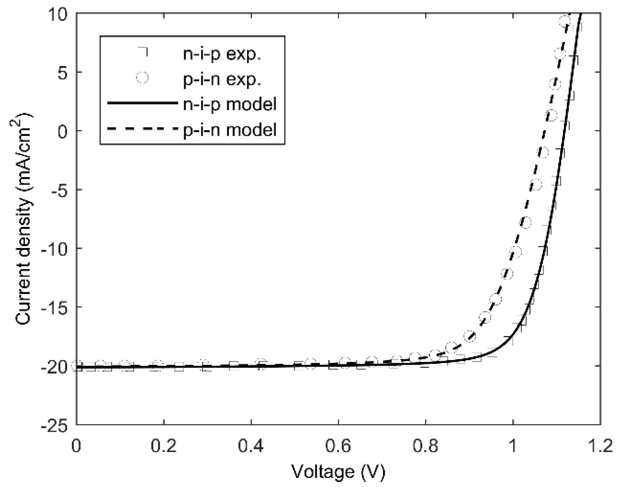
Figure 1 shows the J-V curves of MAPbI3-based cells having both p-i-n and n-i-p structures [11]. The compositions of p-i-n and n-i-p structures are ITO/TaTm/MAPbI3/PCBM/Ag and ITO/PCBM/MAPbI3/TaTm/Au, respectively. The experimental data are extracted from Figure 4 of Ref. [25]. The symbols, dashed, and solid lines represent the experimental results and the model fit to the experimental results of p-i-n and n-i-p structures, respectively. The extracted physical parameters for the p-i-n structures, by fitting the experimental data, are Rs = 5 Ω·cm2, Rp > 104 Ω·cm2, Jc = 2.06 × 10⁻⁸ mAcm−2 and τe = τh = 15 ns, whereas, for the n-i-p structure, the parameters are Rs = 3 Ω·cm2, Rp > 104 Ω·cm2, Jc = 7.15 × 10⁻⁹ mAcm−2 and τe = τh = 20 ns. The dark current is three times larger and the transport property is slightly inferior in the p-i-n structure. As such, both the open circuit voltage and the power conversion efficiency (PCE) are higher in the n-i-p structure (PCE = 17.9 and 16.06 in n-i-p and p-i-n structures, respectively). The performance improvement in the n-i-p structure is due to the reduction in forward dark current via better heterojunction alignment.
3.2. MAPbI3−xClx-Based Cells
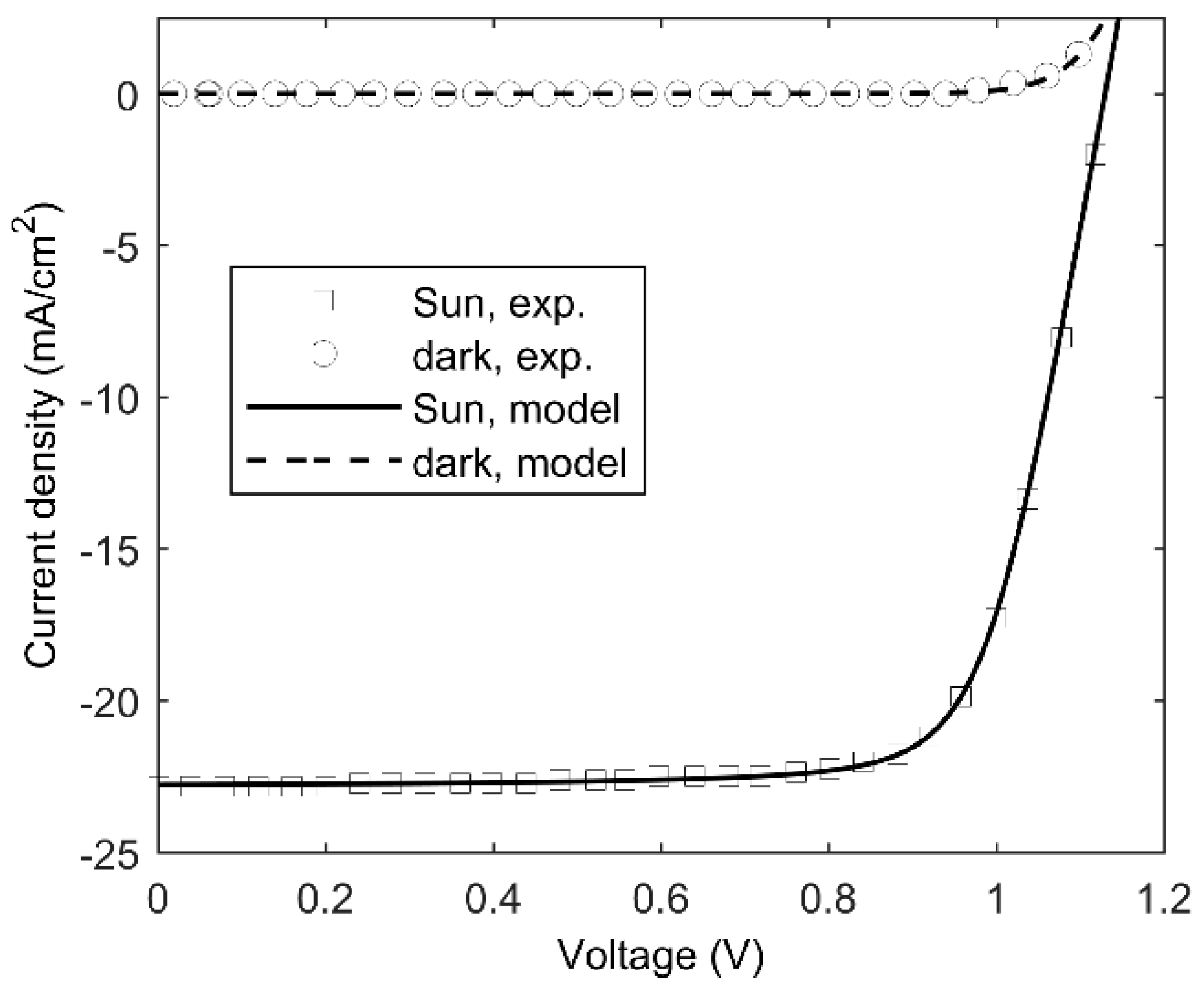
The current–voltage characteristics of a MAPbI3−xClx-based solar cell are shown in Figure 2. The composition of the n-i-p structure is ITO/TiO2/MAPbI3−xClx/spiro-OMeTAD/Au. The experimental data are extracted from Figure 3 of Ref. [1]. The symbols, dashed, and solid lines represent the experimental results and the model fit to the experimental results of dark and sun illumination, respectively. The extracted physical parameters are Rs = 6.5 Ω·cm2, Rp > 2 × 10⁴ Ω·cm2, Jc = 2.62 × 10⁻⁹ mAcm−2, and τe = τh = 12 ns. The power conversion efficiency (PCE) is 19.4%. The PCE improvement in this cell as compared to previous MAPbI3 cells is due to the slightly broader-spectrum absorption and lower dark current. The model shows excellent agreement with the experimental results on both the dark and net currents.
3.3. FAPbI3-Based Cells
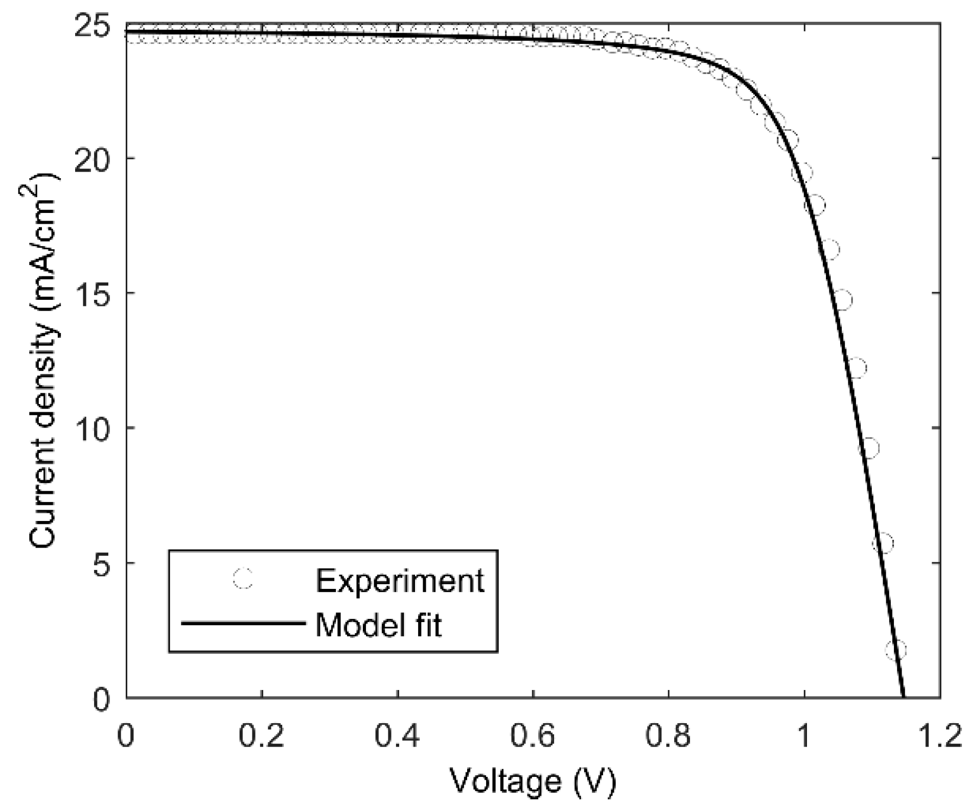
Figure 3 shows the current–voltage characteristics of a FAPbI3-based solar cell. The composition of the n-i-p structure is ITO/TiO2/(FAPbI3)0.85 (MAPbBr3)/spiro-OMeTAD/Au. The experimental data are extracted from Figure 3 of Ref. [3]. The net current is considered positive in Figure 3. The symbols and solid line represent the experimental results and the model fit to the experimental results, respectively. The extracted physical parameters are Rs = 5.7 Ω·cm2, Rp > 2 × 10⁴ Ω·cm2, Jc = 2.99 × 10⁻⁹ mAcm−2, and τe = τh = 15 ns. The power conversion efficiency (PCE) is 20.8%. The further improvement in PCE is due to further absorption of the lower spectrum. The extracted value of the mobility lifetime product is 1.2 × 10⁻⁷ cm2V−1. The extracted parameters for these three types of perovskite solar cells are summarized in Table 1.
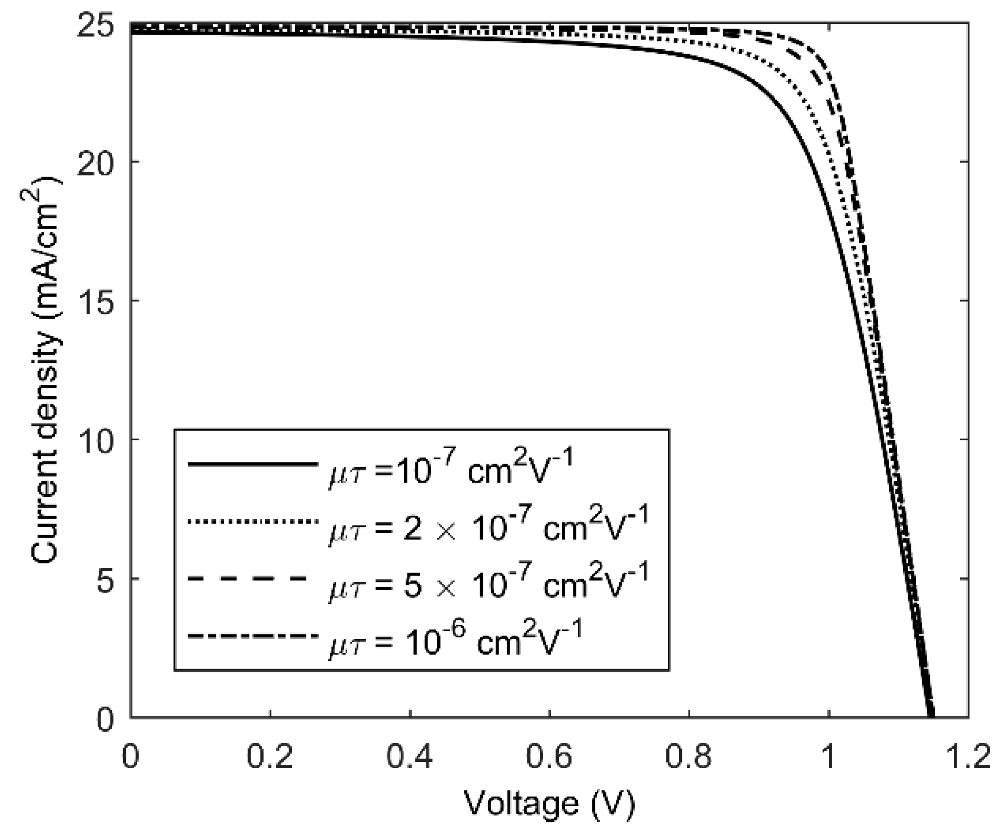
The fill factor and PCE can be improved further by simply improving the carrier transport. The expected effect of carrier transport on the J-V characteristics of the same cell is shown in Figure 4. The improvement in charge carrier transport mainly enhances the fill factor and PCE. The PCE is enhanced to a value of 23.4% by one order of magnitude, improving the mobility lifetime product of carriers. There is also a slight increase in the short circuit current.
4. Conclusions
In this paper, physics-based compact mathematical models for the external voltage-dependent forward dark and photocurrent in perovskite solar cells have been developed by considering the charge carrier transport properties in the bulk material. The theoretical models are verified by comparing the model calculations with published experimental results on various perovskite solar cells, which reveals useful carrier transport and cell parameters. The model shows excellent agreement with the experimental results. Further improvement in the charge carrier transport in the perovskite layer will enhance the fill factor and hence the power conversion efficiency. The physics-based compact model of this paper can serve as a tool for extracting charge carrier transport and cell parameters and improving the required areas of material properties and device structure.
Funding
This research received no external funding.
Institutional Review Board Statement
Not applicable.
Informed Consent Statement
Not applicable.
Data Availability Statement
The study did not report any data.
Conflicts of Interest
The author declares no conflict of interest.
References
- Zhou, H.; Chen, Q.; Li, G.; Luo, S.; Song, T.; Duan, H.S.; Hong, Z.; You, J.; Liu, Y.; Yang, Y. Interface engineering of highly efficient perovskite solar cells. Science 2014, 345, 542–546. [Google Scholar] [CrossRef] [PubMed]
- Yang, W.S.; Noh, J.H.; Jeon, N.J.; Kim, Y.C.; Ryu, S.; Seo, J.; Seok, S. High-performance photovoltaic perovskite layers fabricated through intramolecular exchange. Science 2015, 348, 1234–1237. [Google Scholar] [CrossRef]
- Bi, D.; Tress, W.; Dar, M.I.; Gao, P.; Luo, J.; Renevier, C.; Schenk, K.; Abate, A.; Giordano, F.; Baena, J.P.C.; et al. Efficient luminescent solar cells based on tailored mixed-cation perovskites. Sci. Adv. 2016, 2, 1501170. [Google Scholar] [CrossRef] [PubMed] [Green Version]
- Wahid, S.; Islam, M.; Rahman, M.S.S.; Alam, M.K. Transfer matrix formalism-based analytical modeling and performance evaluation of perovskite solar cells. IEEE Tran. Elec. Devices 2017, 64, 5034–5041. [Google Scholar] [CrossRef]
- Lu, Y.B.; Yang, H.; Cong, W.Y.; Zhang, P. Temperature dependence of the effective mass of the hybrid organic-inorganic perovskites CH3NH3PbI3. Appl. Phys. Lett. 2017, 111, 253902. [Google Scholar] [CrossRef]
- Llanos, A.; Thibau, E.S.; Lu, Z.H. Abnormal thin film structures in vapor-phase deposited methylammonium lead iodide perovskite. J. Vac. Sci. Technol. A 2016, 34, 060601. [Google Scholar] [CrossRef]
- Bokdam, M.; Sander, T.; Stroppa, A.; Picozzi, S.; Sharma, D.D.; Franchini, C.; Kresse, G. Role of polar phonons in the photo excited state of metal halide perovskites. Sci. Rep. 2016, 6, 28618. [Google Scholar] [CrossRef] [Green Version]
- Motta, C.; El-Mellouhi, F.; Sanvito, S. Charge carrier mobility in hybrid halide perovskites. Sci. Rep. 2015, 5, 12746. [Google Scholar] [CrossRef]
- Brenner, T.M.; Egger, D.A.; Kronik, L.; Hodes, G.; Cahen, D. Hybrid organic–inorganic perovskites: Low-cost semiconductors with intriguing charge-transport properties. Nat. Rev. Mater. 2016, 1, 15007. [Google Scholar] [CrossRef]
- Kim, H.S.; Jang, I.H.; Ahn, N.; Choi, M.; Guerrero, A.; Bisquert, J.; Park, N.G. Control of I-V hysteresis in CH3NH3PbI3 perovskite solar cell. J. Phys. Chem. Lett. 2015, 6, 4633–4639. [Google Scholar] [CrossRef]
- Momblona, C.; Escrig, L.G.; Bandiello, E.; Hutter, E.M.; Sessolo, M.; Lederer, K.; Nimoth, J.B.; Bolink, H.J. Efficient vacuum deposited p-i-n and n-i-p perovskite solar cells employing doped charge transport layers. Energy Environ. Sci. 2016, 9, 3456. [Google Scholar] [CrossRef]
- Asif, A.A.; Singha, R.; Alapattb, G.F. Technical and economic assessment of perovskite solar cells for large scale manufacturing. J. Renew. Sustain. Energy 2015, 7, 043120. [Google Scholar] [CrossRef] [Green Version]
- Richardson, G.; O’Kane, S.E.J.; Niemann, R.G.; Peltola, T.A.; Foster, J.M.; Cameron, P.J.; Walker, A.B. Can slow-moving ions explain hysteresis in the current–voltage curves of perovskite solar cells? Energy Environ. Sci. 2016, 9, 1476–1485. [Google Scholar] [CrossRef] [Green Version]
- Sherkar, T.S.; Momblona, C.; Gil-Escrig, L.; Bolink, H.J.; Koster, L.J.A. Improving Perovskite Solar Cells: Insights From a Validated Device Model. Adv. Energy Mater. 2017, 7, 1602432. [Google Scholar] [CrossRef] [Green Version]
- Sun, X.; Asadpour, R.; Nie, W.; Mohite, A.D.; Alam, M.A. A Physics-based analytical model for perovskite solar cells. IEEE J. Photovolt. 2015, 5, 1389–1394. [Google Scholar] [CrossRef]
- Huang, J.; Yuan, Y.; Shao, Y.; Yan, Y. Understanding the physical properties of hybrid perovskites for photovoltaic applications. Nat. Rev. Mater. 2017, 2, 17042. [Google Scholar] [CrossRef]
- Saleheen, M.M.; Arnab, S.M.; Kabir, M.Z. Analytical model for voltage-dependent photo and dark currents in bulk heterojunction organic solar cells. Energies 2016, 9, 412. [Google Scholar] [CrossRef] [Green Version]
- Nelson, J. The Physics of Solar Cells; Imperial College Press: London, UK, 2003. [Google Scholar]
- Mannan, M.A.; Anjan, M.S.; Kabir, M.Z. Modeling of the current-voltage characteristics of thin film solar cells. Solid State Electronics 2011, 63, 49–54. [Google Scholar] [CrossRef]
- Anjan, M.S.; Kabir, M.Z. Modeling of current-voltage characteristics of CdS/CdTe solar cells. Phys. Status Solidi A 2011, 208, 1813–1816. [Google Scholar] [CrossRef] [Green Version]
- Shockley, W. Currents to conductors induced by a moving point charge. J. Appl. Phys. 1938, 9, 635–636. [Google Scholar] [CrossRef]
- He, Z. Review of the shockley-ramo theorem and its application in semiconductor gamma-ray detectors. Nucl. Instr. Meth. Phys. Res. A 2001, 463, 250–267. [Google Scholar] [CrossRef]
- Hernández-García, L.F.; Cabrera-Arenas, V.; Reséndiz-Mendoza, L.M. On the convergence of the algorithm for simulating organic solar cells. Comput. Phys. Commun. 2015, 196, 372–379. [Google Scholar] [CrossRef]
- National Renewable Energy Laboratory. Available online: http://rredc.nrel.gov/solar/spectra/am1.5/ (accessed on 24 June 2021).
- Sherkar, T.S.; Momblona, C.; Gil-Escrig, L.; Ávila, J.; Sessolo, M.; Bolink, H.J.; Koster, L.J.A. Recombination in perovskite solar cells: Significance of grain boundaries, interface traps, and defect ions. ACS Energy Lett. 2017, 2, 1214–1222. [Google Scholar] [CrossRef] [PubMed]
Figure 1.
Current−voltage characteristics of a MAPbI3-based solar cell. The experimental data are extracted from Figure 4 of Ref. [25].
Figure 1.
Current−voltage characteristics of a MAPbI3-based solar cell. The experimental data are extracted from Figure 4 of Ref. [25].

Figure 2.
Current−voltage characteristics of a MAPbI3−xClx-based solar cell. The experimental data are extracted from Figure 3 of Ref. [1].
Figure 2.
Current−voltage characteristics of a MAPbI3−xClx-based solar cell. The experimental data are extracted from Figure 3 of Ref. [1].

Figure 3.
Current−voltage characteristics of a FAPbI3-based solar cell. The net current is considered positive here. The experimental data are extracted from Figure 3 of Ref. [3].
Figure 3.
Current−voltage characteristics of a FAPbI3-based solar cell. The net current is considered positive here. The experimental data are extracted from Figure 3 of Ref. [3].

Figure 4.
Effect of carrier transport on current–voltage characteristics of a FAPbI3-based solar cell. The net current is considered positive here.
Figure 4.
Effect of carrier transport on current–voltage characteristics of a FAPbI3-based solar cell. The net current is considered positive here.


Table 1.
The extracted parameters for various perovskite solar cells.
| Cell Materials/Structure | Vbi (V) | Jc (mA/cm2) | Rs (Ω·cm2) | µτ (cm2/V) | PCE (%) |
|---|---|---|---|---|---|
| MAPbI3/p-i-n [25] | 1.2 | 20.6 × 10⁻⁹ | 5 | 1.2 × 10⁻⁷ | 16.06 |
| MAPbI3/n-i-p [25] | 1.12 | 7.15 × 10⁻⁹ | 3 | 1.6 × 10⁻⁷ | 17.9 |
| MAPbI3−xClx/n-i-p [1] | 1.15 | 2.62 × 10⁻⁹ | 6.5 | 0.96 × 10⁻⁷ | 19.4 |
| (FAPbI3)0.85 (MAPbBr3)/n-i-p [3] | 1.15 | 2.99 × 10⁻⁹ | 5.7 | 1.2 × 10⁻⁷ | 20.8 |
Publisher’s Note: MDPI stays neutral with regard to jurisdictional claims in published maps and institutional affiliations. |
© 2021 by the author. Licensee MDPI, Basel, Switzerland. This article is an open access article distributed under the terms and conditions of the Creative Commons Attribution (CC BY) license (https://creativecommons.org/licenses/by/4.0/).
Share and Cite
MDPI and ACS Style
Kabir, M.Z. A Physics-Based Analytical Model for Current–Voltage Characteristics of Perovskite Solar Cells Incorporating Bulk Recombination. Energies 2021, 14, 3868. https://0-doi-org.brum.beds.ac.uk/10.3390/en14133868
AMA Style
Kabir MZ. A Physics-Based Analytical Model for Current–Voltage Characteristics of Perovskite Solar Cells Incorporating Bulk Recombination. Energies. 2021; 14(13):3868. https://0-doi-org.brum.beds.ac.uk/10.3390/en14133868
Chicago/Turabian StyleKabir, M. Zahangir. 2021. "A Physics-Based Analytical Model for Current–Voltage Characteristics of Perovskite Solar Cells Incorporating Bulk Recombination" Energies 14, no. 13: 3868. https://0-doi-org.brum.beds.ac.uk/10.3390/en14133868
Note that from the first issue of 2016, this journal uses article numbers instead of page numbers. See further details here.