Article

Misalignment-Tolerant Series Hybrid with Active Adjustable Constant Current and Constant Voltage Output Wireless Charging System

1
School of Electrical Engineering, Xi’an University of Technology, 58, Yanxiang Rd., Xi’an 710054, China
2
School of Electronic Information Engineering, Xi’an Technological University, 2, Xuefu Rd., Xi’an 710021, China
*
Author to whom correspondence should be addressed.
Submission received: 12 October 2021 / Revised: 5 November 2021 / Accepted: 10 November 2021 / Published: 13 November 2021

Abstract

:
This paper presents a series hybrid wireless charging system with an active adjustable circuitry offering constant current and constant voltage output characteristics. The series hybrid system consists of the inductor–capacitor–capacitor (LCC) and series-series (SS) networks are used for improving charging pad misalignment tolerance. An active switch is employed to provide an adjustable CC and CV output for different battery charging stages. To demonstrate the performance of the proposed method, a 310 W prototype was built. A systematic optimization in the parameter of the proposed topology to achieve relative constant output was analyzed within a certain range of the designed operating region. The experimental results indicate that the output current fluctuation is less than 5% with load variations, and the output voltage fluctuation is less than 5% with load varying from 19 to 70 Ω, as the pick-up pads misaligned within 50% of the pad outer diameter.

1. Introduction

Wireless power transfer (WPT) systems using an alternating magnetic field to transfer power across a relatively large air gap have been adopted in numerous industrial and commercial applications. In comparison to traditional plug-in charging technology, WPT is safe offering galvanic isolation, maintenance free with dirt and moisture environments [1,2,3,4,5,6], and has great potential to be used in, for example, electric vehicle (EV) charging, portable electronics, autonomous underwater vehicles (AUVs), and implantable biomedical devices [7,8,9,10,11], etc.
As for practical battery charging applications, the equivalent resistance of the battery varies significantly when considering the entire charging process. Thus, charging with a wide range of loading conditions to achieve the constant current (CC) output and constant voltage (CV) output is essential for most of the li-ion battery charging applications [12]. Specific to wireless charging scenarios, misalignment between magnetic couplers results in variation of the self and mutual inductance, and poses a negative impact on the current, voltage outputs, and transfer efficiency. Thus, the motivation of this paper is to design a WPT system, which is able to provide CC output and CV output with a wide range of loads and high misalignment tolerance between the primary and pickup magnetic couplers.
In the past few years, many approaches have been investigated to realize the desired current or voltage under different loading conditions for a WPT system. The DC-DC converter at the primary side or the secondary side is employed to regulate the current or voltage output [13,14]. However, this additional cascading DC-DC converter will result in extra converter loss and cost, and need extra space for setting up the device. Variable frequency control and phase shift control of the WPT system can also be used to realize the CV or CC output against load and coupling variations [15,16,17]. However, variable frequency control may result in the frequency bifurcation phenomenon in a certain loading condition with a reduced power transmission capability [18]. In addition, the phase shift control has difficulty realizing the input zero phase angle (ZPA). Furthermore, these closed-loop control methods all require feedback signals from the pick-up side, which may result in control failure when wireless communication is disturbed. To solve these drawbacks, compensation topologies to obtain relative CC or CV output without the complicated control approaches have also been investigated. A variable coil structure for WPT system CC and CV output, which consists of two DD coils and one Q coil on the transmitter side, is systematically analyzed in [19]. In [20], a variable-parameter T-circuit on the primary side is used to regulate the output current and voltage, reducing the number of passive components. However, these variable structures on the transmitter side allow the WPT system to operate with the desired CC and CV output at the expense of extra wireless communication, which can result in additional system cost and control failure due to external interference. In order to solve the deficiency of wireless communication, some new variable compensation topologies at the receiver side, such as series–series (SS) and series–inductor–capacitor–capacitor (S-LCC), or inductor–capacitor–capacitor–series (LCC-S) and LCC-LCC topologies for CC and CV outputs, are introduced in [21,22]. Nonetheless, all the compensation topologies aforementioned can achieve desired CC and CV outputs when the magnetic couplers are perfectly aligned at a fixed position. Otherwise, the misalignment may seriously affect the current and voltage output due to parameter variations.
The misalignment of the coupling pads is expected in practical applications, which may result in decreasing power transmission capability, reducing the transmission efficiency, and instability of the system. Thus, to maintain constant power when the misalignment occurs, a practical WPT application is necessary. Numerous approaches, such as control techniques, proper magnetic structures, and hybrid circuit topologies, have been used to mitigate this problem.
Many new control strategies have been proposed [23,24,25,26] to maintain stable outputs under pad misalignment conditions. However, these controllers usually need wireless communication to obtain the feedback signals from the secondary side, and regulate the power flow. The communications may result in instability of the WPT systems, regardless of the extra volume and cost. In order to solve these defects, considerable efforts have been made to design proper magnetic couplers, such as three-dimensional (3D) quadrature-shaped coils [27], bipolar and double-D (DD) coils [28], quadruple-D quadrature pads (QDQP) [29], and an unsymmetrical coupling structure [30]. These magnetic couplers can provide a relatively uniform magnetic field distribution to improve the misalignment tolerance. Meanwhile, hybrid topologies, which are an alternative method used to improve the misalignment tolerance, have recently been introduced in [29,31,32,33]. For example, in [29], an input-parallel–output-series hybrid system was built, which consists of LCC-S and S-LCC topologies. The new compensation topology can maintain the output voltage within 5% fluctuations, when 50% longitudinal misalignment occurs. The series-hybrid and parallel-hybrid topologies are presented in [31,32], with the combination of LCC-LCC and SS topologies, which were connected in series and parallel types of the primary and pick-up sides, separately, to achieve constant power throughput. A family of hybrid WPT topologies is discussed in detail in [33], which can extend the tolerant misalignment. However, all these approaches above cannot achieve both CC output and CV output with high misalignment.
An input-parallel–output-series hybrid and configurable system is proposed in [34], which can provide relatively constant CC and CV outputs, within 50% longitudinal misalignment. However, when the pick-up pads move out of the operating region, the current of the parallel SS compensation network in the primary side may increase too much to break down the inverter, which is caused by the decrease in reflected impedance due to the decreasing coupling. Although using a closed-loop controller can suppress this increase current and protect the inverter, it may significantly reduce the system efficiency and reliability.
This paper presents a novel series hybrid and configurable compensation topology to achieve CC and CV outputs with high misalignment tolerance. Additionally, the main contributions of this paper are summarized as follows:
(1) The proposed series hybrid compensation topology can achieve load-independent CC output, and realize operation without pickup side coils, which can overcome the aforementioned drawbacks associated with [34], and limit the current of the inverter without extra controllers. In addition, a set of parameter optimization is proposed to improve the constancy in output power when misalignment occurs.
(2) A variable structure T-circuit is employed to transfer CC output to CV output without an additional cascade converter, and owns a native load-independent character, which can simplify the control schemes.
Specifically, Section 2 analyzes the mathematical model of the series hybrid and configurable topology. The changes in the inductances of the DDQ pads between primary and pick-up sides, and the parameter optimization are presented in Section 3. In Section 4, a 310 W prototype that was built to verify the theoretical analysis is described. Finally, the conclusion is drawn in Section 5.

2. Theoretical Analysis

Figure 1 shows the proposed series hybrid and configurable topology. The high frequency inverter and full-bridge rectifier consists of four MOSFETs (Q1–Q4) and four diodes (D1–D4), respectively. An inductor L0 and capacitors C0 and C1 (L5, C5 and C2) constitute the LCC-LCC compensation topology, while capacitor C3 (C4) is part of the SS compensation topology. LCC-LCC and SS topologies of the primary and pick-up sides are both connected in series, together making up the LCC-S series hybrid topology, and the configurable topology is formed with inductors Lf1 and Lf2 and capacitor Cf, together with switches S1 and S2. M12 and M34 are the main mutual inductances, while M13, M14, M23, and M24 are the cross mutual inductances. The analysis of the proposed system is based on the fundamental harmonic approximation method and the influence of the higher harmonics is ignored.

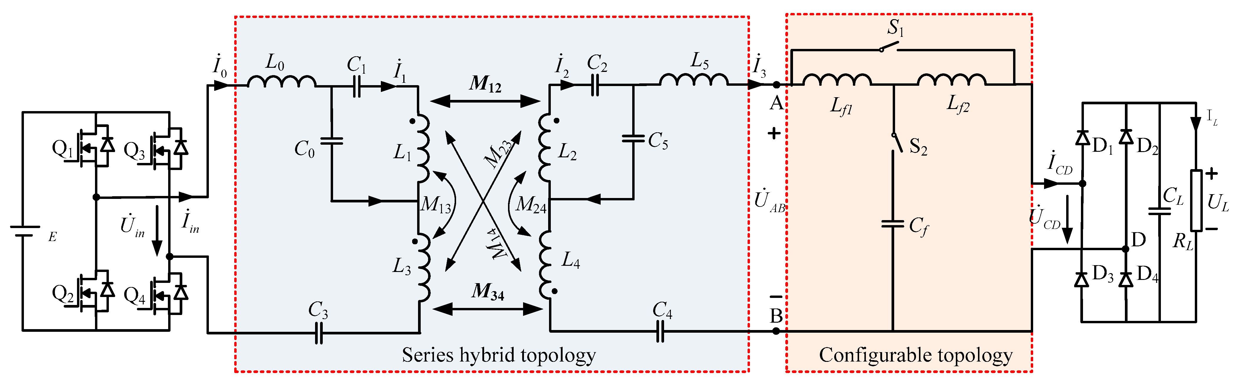
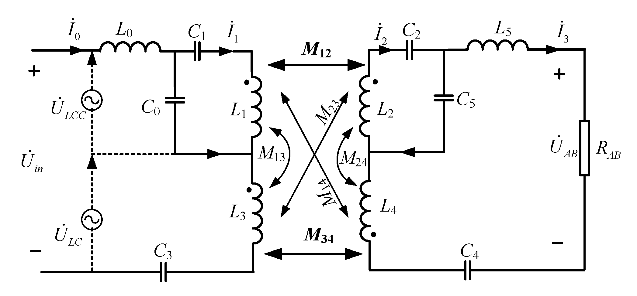
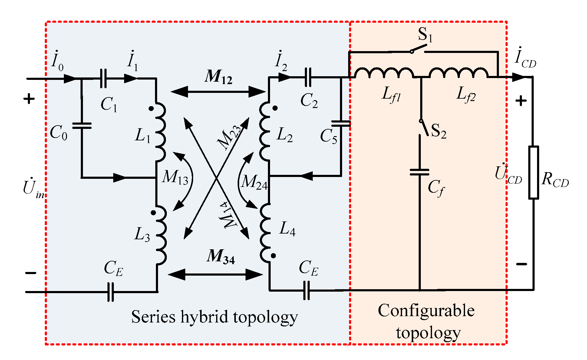
2.1. Analysis of the Series Hybrid Topology

Figure 2 illustrates the series hybrid topology, which is driven by a resonant inverter with angular frequency ω. In order to tune the LCC-S series hybrid compensation network in the primary and pick-up sides to the constant resonant frequency, the resonant parameters are designed to satisfy the following equations:
{ ω 2 L 0 C 0 = ω 2 L 1 C 0 C 1 C 0 + C 1 = 1 ω 2 L 5 C 5 = ω 2 L 2 C 2 C 5 C 2 + C 5 = 1 . ω 2 L 3 C 3 = ω 2 L 4 C 4 = 1
According to Figure 2, Kirchhoff’s voltage law is used to describe the relationship of voltages in the series hybrid circuit; therefore, we can obtain:
[ Z 00 Z 01 Z 02 Z 03 Z 10 Z 11 Z 12 Z 13 Z 20 Z 21 Z 22 Z 23 Z 30 Z 31 Z 32 Z 33 ] [ I ˙ 0 I ˙ 1 I ˙ 2 I ˙ 3 ] = [ U ˙ i n 0 0 0 ]
where:
Z 00 = j ω L 0 + ( j ω C 0 ) 1 + j ω L 3 + ( j ω C 3 ) 1   , Z 01 = ( j ω C 0 ) 1 + j ω M 13 , Z 02 = j ω M 23 , Z 03 = j ω M 34 , Z 10 = j ω M 13 ( j ω C 0 ) 1 , Z 11 = j ω L 1 + ( j ω C 0 ) 1 + ( j ω C 1 ) 1 , Z 12 = j ω M 12 , Z 13 = j ω M 14 , Z 20 = j ω M 23 , Z 21 = j ω M 12   , Z 22 = j ω L 2 + ( j ω C 2 ) 1 + ( j ω C 5 ) 1 , Z 23 = ( j ω C 5 ) 1 + j ω M 24 , Z 30 = j ω M 34   , Z 31 = j ω M 14 , Z 32 = ( j ω C 5 ) 1 j ω M 24 , Z 33 = j ω L 5 + ( j ω C 5 ) 1 + j ω L 4 + ( j ω C 4 ) 1 + R A B .
In order to simplify the analysis, only the main couplings (M12 and M34) are taken into consideration, while the cross couplings (M13, M14, M23, and M24) can be ignored by designing proper coupling structures, which will be discussed in Section 3. Hence, the current of the inverter, the current of the L1 transmitter, the current of the L2 receiver, and the current of the RAB load are obtained as:
{ I ˙ 0 = U ˙ i n ω 2 M 12 2 R A B ( L 0 L 5 + M 12 M 34 ) 2 I ˙ 1 = U ˙ i n j ω L 5 L 0 L 5 + M 12 M 34 I ˙ 2 = U ˙ i n ω 2 L 0 M 12 R A B ( L 0 L 5 + M 12 M 34 ) 2 I ˙ 3 = U ˙ i n j ω M 12 L 0 L 5 + M 12 M 34
Then, according to the current I ˙ 0 of the inverter, the input equivalent impedance Zin of the system can be deduced as:
Z i n = ω 2 ( L 0 L 3 + M 12 M 34 ) 2 M 12 2 R A B  
According to (3) and (4), the current I ˙ 0 is in the same phase with the inverter output voltage U ˙ i n , and the input impedance of the system is pure resistance. When the whole system works in the full tuned condition, the input reactive power is zero, which can improve the transmission efficiency of the system. In addition, the current I ˙ 0 and the input equivalent impedance Zin clearly indicate that the inverter current is close to zero when the pick-up sides move far away, which means the mutual inductance is close to zero. Therefore, the series hybrid system can avoid the extreme situation that the inverter output current is too high to burn down due to the no-load operation of the parallel SS structure, and improve the reliability of the system.
Equation (3) shows that the output current I ˙ 3 is load independent and lags the inverter output voltage by 90°.

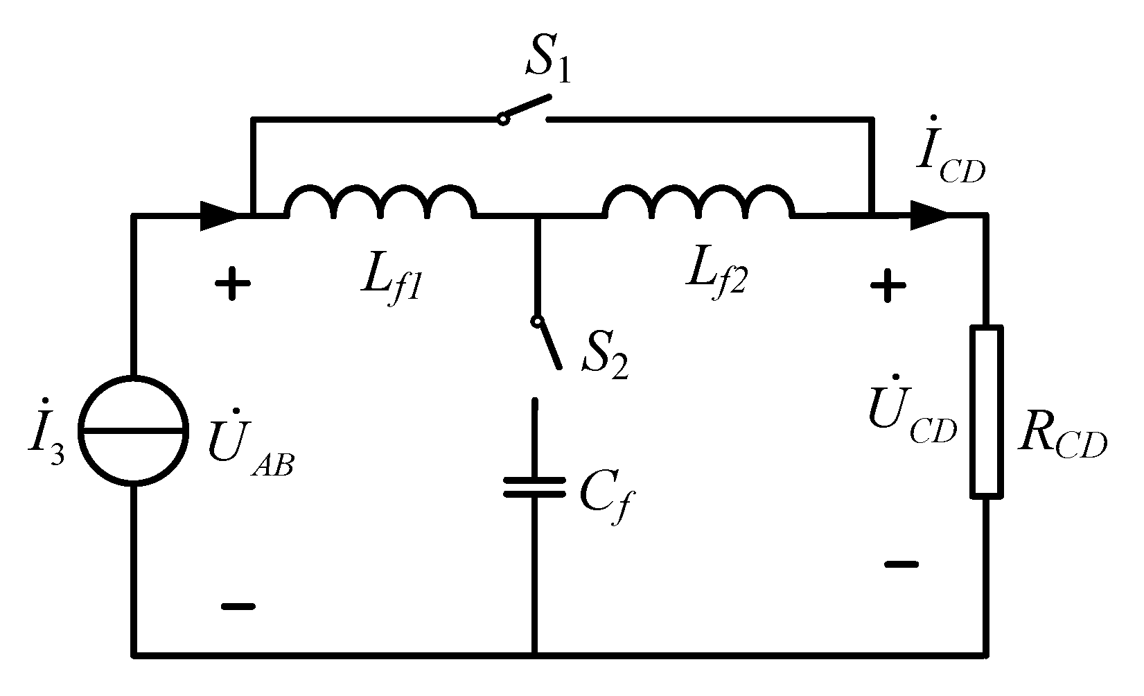
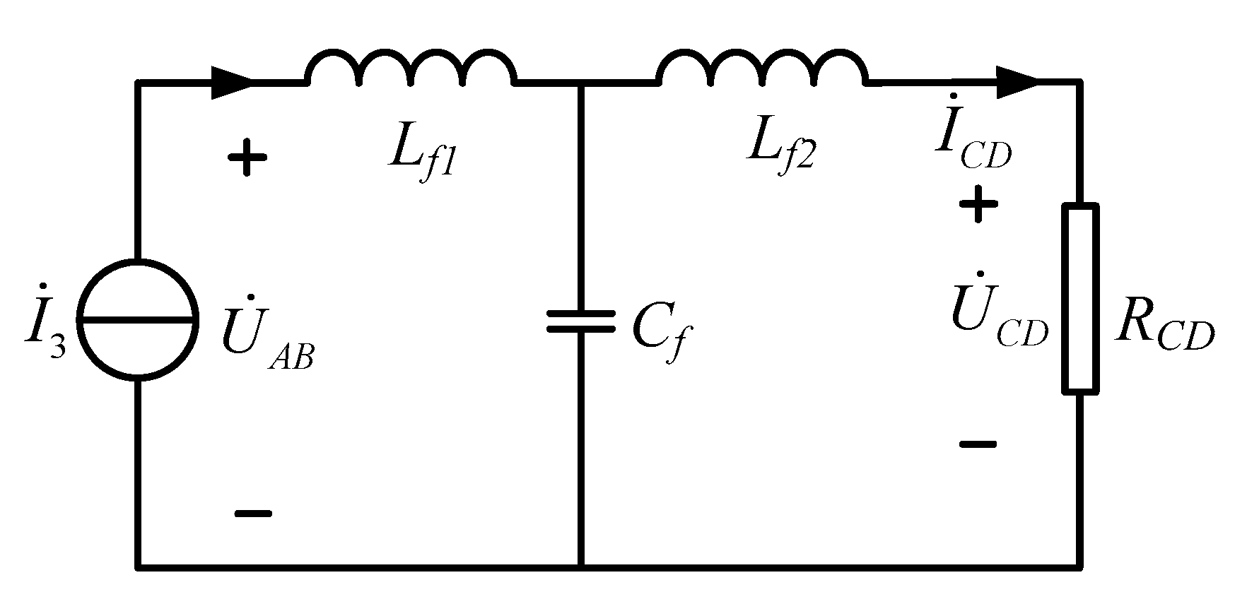
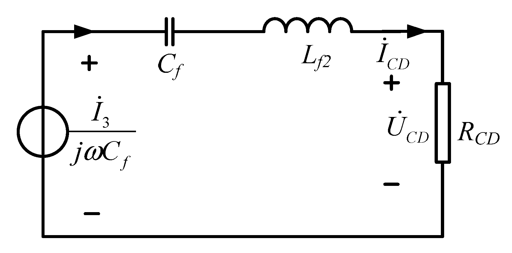
2.2. Analysis of the Configurable Topology

Figure 3 shows the equivalent circuit of the configurable topology is driven by a current source, because the series hybrid topology circuit can obtain load-independent constant current output. When the function switch S1 is ON and S2 is OFF, the system provides CC output, and the output current I ˙ C D is shown as:
I ˙ C D = I ˙ 3
The input equivalent impedance Zcc-AB is expressed as:
Z c c - A B = R C D
When the S1 is OFF and S2 is ON, the system provides CV output, as is shown in Figure 4. The relationship between inductors Lf1 and Lf2 and capacitor Cf satisfies the following equations, i.e.,
{ j ω L f 1 + 1 j ω C f = 0 j ω L f 2 + 1 j ω C f = 0
Then, according to Thevenin–Norton theorems, the input voltage shown in Figure 5 can be described by:
U ˙ A B = I ˙ 3 j ω C f
Equation (6) indicates that the inductor Lf2 and capacitor Cf form the resonant network tank; therefore, the output voltage is:
U ˙ C D = I ˙ 3 j ω C f
The input equivalent impedance Zcv-AB is expressed as:
Z c v - A B = L f 1 C f R C D

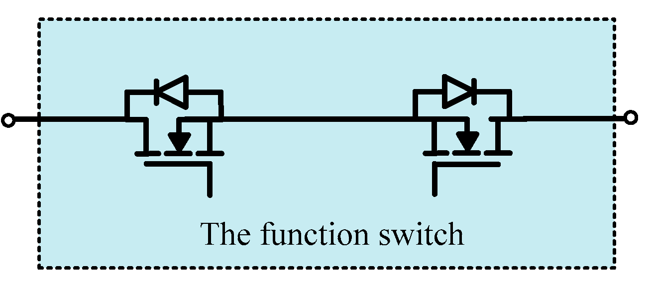
2.3. The Proposed Combination of Series Hybrid and Configurable Topology

Figure 6 shows the equivalent circuit with the series hybrid and the configurable topology. Comparing Figure 1 with Figure 6, the capacitor CE is used to substitute the inductor L0 (L5) and capacitor C3 (C4). The component CE can be expressed by:
j ω L 0 + 1 j ω C 3 = 1 j ω C E
or:
j ω L 5 + 1 j ω C 4 = 1 j ω C E
From (3) and (5), when the system operates in CC output, the output current is:
I ˙ C D = U ˙ i n j ω M 12 L 0 L 5 + M 12 M 34
Additionally, the corresponding input impedance Zin-cc is expressed by:
Z i n - c c = ω 2 ( L 0 L 5 + M 12 M 34 ) 2 M 12 2 R C D
From (3) and (8), when the system operates in CV output, the output voltage is:
U ˙ C D = U ˙ i n M 12 ω 2 C f ( L 0 L 5 + M 12 M 34 )
Additionally, the corresponding input impedance Zin-cv is expressed by:
Z i n - c c = ω 2 ( L 0 L 5 + M 12 M 34 ) 2 C f R C D M 12 2 L f 1
According to (12) and (14), the value of L0L5/M12 will increase, while the value of M34 will decrease, when the main mutual inductances M12 and M34 decrease with pad misalignment. Thus, the sum of L0L5/M12 and M34 can remain relatively constant within a certain range of misalignment when the parameters are properly designed. Then, a constant current and voltage output with pad misalignment can be achieved.
From (13) and (15), it illustrates that the input impedance of the system is pure resistance when the series hybrid and configurable topology works in CC output and CV output, which means the output voltage and current of the inverter can achieve a zero phase angle (ZPA).

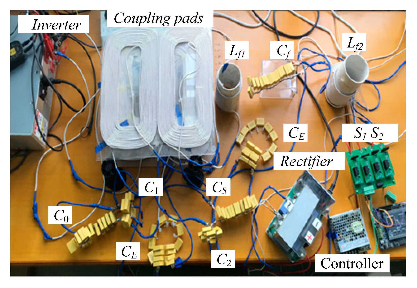
3. Design and Implementation of the Hybrid and Configurable Topology
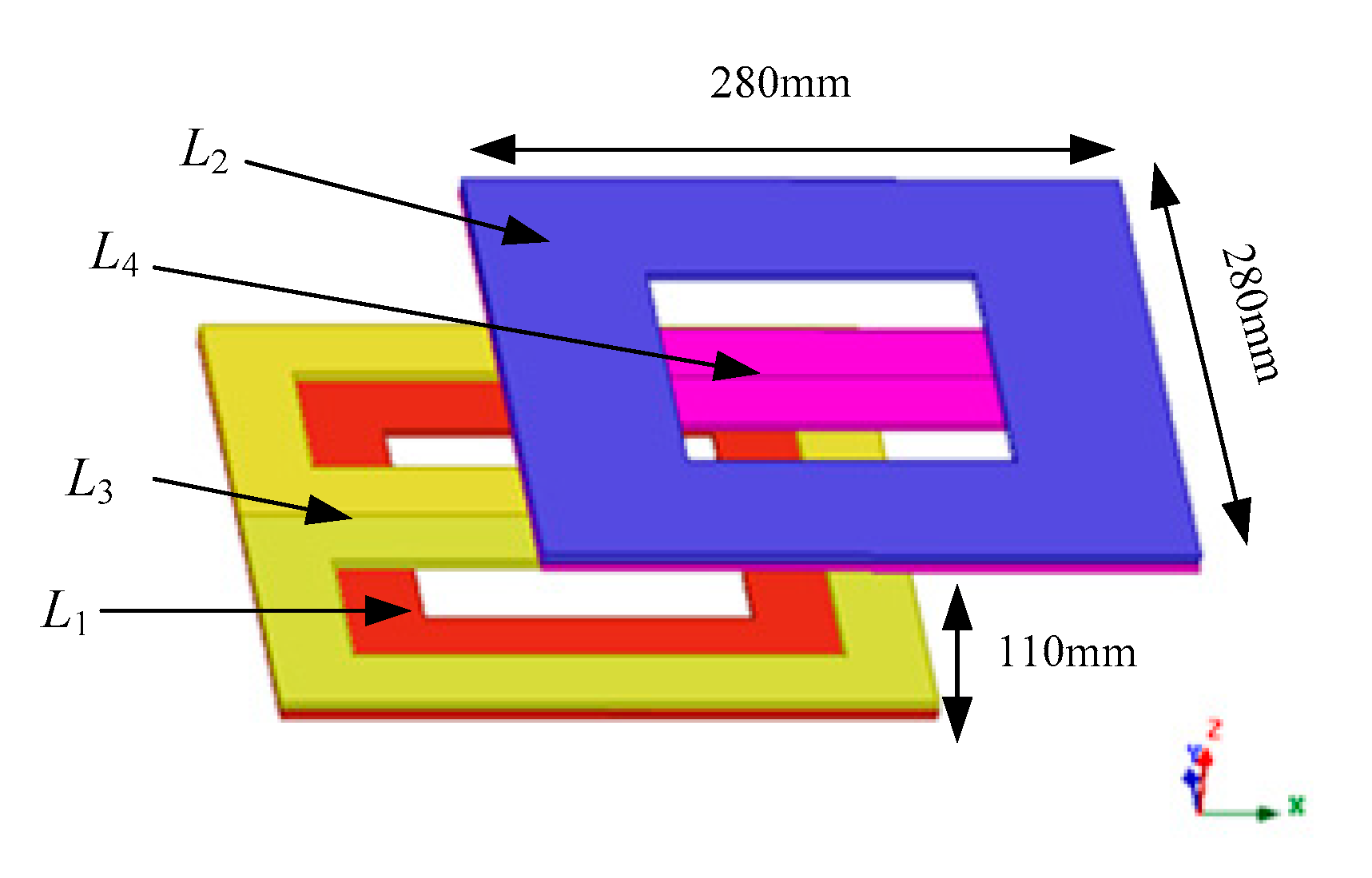
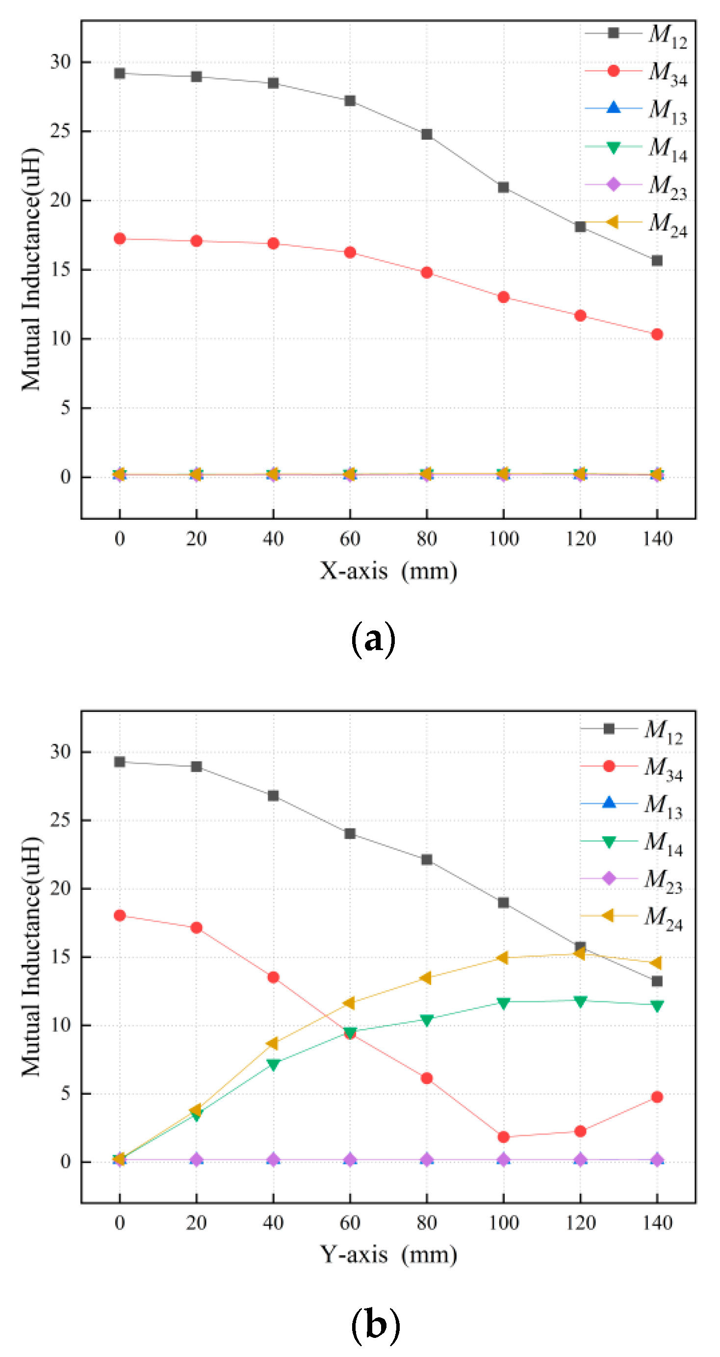
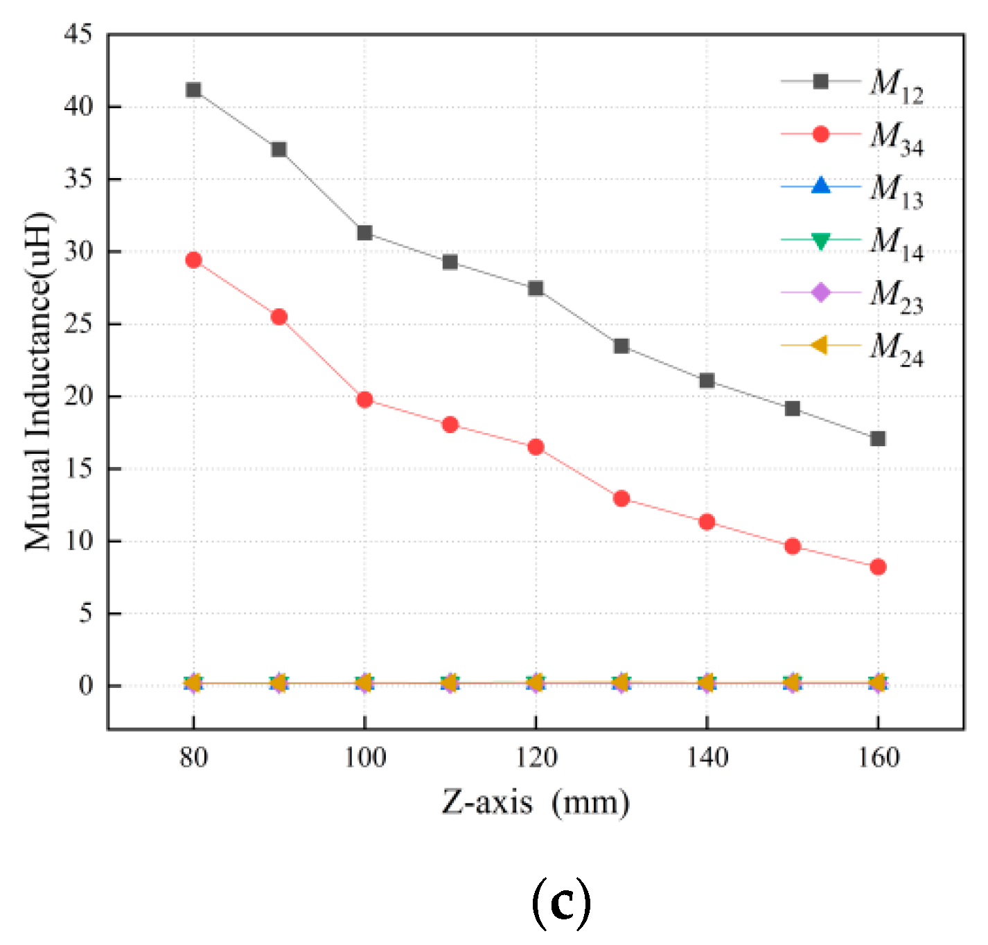
3.1. Coupler Design

According to (3), constant current output can be achieved only when the cross couplings (M13, M14, M23, and M24) are too small to be negligible. Therefore, only the main mutual inductances M12 and M34 are taken into consideration when the magnetic coupler is in misalignment. Additionally, the DDQ and DD structures can satisfy these desired requirements as discussed in [32,33]. Hence, the DDQ structure is used and shown in Figure 7. The Q pad structure is formed by the transmitter L1 and receiver L2, while the DD pad structure is formed by the transmitter L3 and receiver L4. Meanwhile, the misalignment occurrence between the primary and pick-up pads is unavoidable in the charging system, including X-axis misalignment, Y-axis misalignment, and Z-axis misalignment. All the mutual inductances of the DDQ coils are measured when the pick-up pads are moved along the X-axis, Y-axis, and Z-axis, separately.
As is shown in Figure 8, the main mutual inductances M12 and M34 decrease apparently with the increase of X-axis and Z-axis misalignments, while the cross coupling mutual inductances are too small to be neglected, because the Q pad and the DD pad are symmetrically placed in the primary and pick-up side, so that the amount of the magnetic flux that flows into the Q (DD) pad equals the flows out of it. However, when Y-axis misalignment occurs, the main mutual inductances M12 and M34 and the cross coupling mutual inductances M23 and M14 vary significantly, so the proposed system cannot achieve CC output and CV output in the Y-axis misalignment.

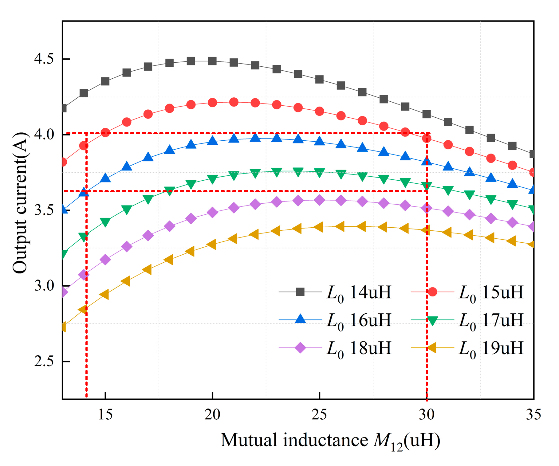
3.2. Parameter Optimization Design

In accordance with the analysis in Section 2, designing proper compensation parameters is of great significance to achieve the relative constant output current and voltage within a certain range of misalignment. In this article, a parameter optimization design method based on inductance L0 and L5 is proposed to ensure relative constant current output of the system.
According to Figure 8a of the X-axis misalignment curves, the relationship between M12 and M34 can be approximately regarded as a linear function:
M 34 = a M 12 + b
where a and b are the coefficients. When the structural parameters of the DDQ coil of the system, such as the material, size, and spacing height of the coil, are changed, resulting in the change trend of main mutual inductances M12 and M34, the parameters a and b need to be recalculated, respectively.
From Figure 8a of the X-axis misalignment curves, the calculated parameters a and b are 0.52 and 2.17 × 10⁻⁶, respectively, and the variation range of the main mutual inductance M12 is [14 uH, 30 uH], then the output current can be expressed as:
I 3 = U i n M 12 ω ( L 0 L 5 + M 12 ( 0.52 M 12 + 2.17 × 10 - 6 ) )
To simplify the analysis, it is assumed that the parameter values of inductance L0 and L5 are equal. Figure 9 shows the output current curves of the system with different inductors L0. It can be found that when the inductor L0 decreases, the output current of the system will increase. In addition, when the main mutual inductance M12 decreases, the system output current shows a trend of increasing first and then decreasing. In this article, the maximum output current of the system is designed to be 4 A, and the allowable deviation of the current is 5%. In other words, the area in the red region of Figure 9 can meet the constant current output under the condition of 50% X-axis offset. Therefore, the inductors L0 and L5 are selected as 16 uH.
According to the measured self-inductance L1 and L2 of Q coils, self-inductance L3 and L4 of DD coils, system resonant angular frequency ω, and inductance L0 and L5 with optimized parameters, the parameters of components, such as capacitors C0, C1, C2, C3, C4, and C5, can be obtained from (1).

4. Experimental Results and Discussion

Figure 10 shows the proposed series hybrid and configurable wireless charging system. The inverter switching devices Q1–Q4 MOSFETs use C2M0080120 and the function switching devices S1–S2 MOSFETs use SPW47N60C3. An electronic load is used to verify the performance of the CC and CV output. The system parameters are listed in Table 1.

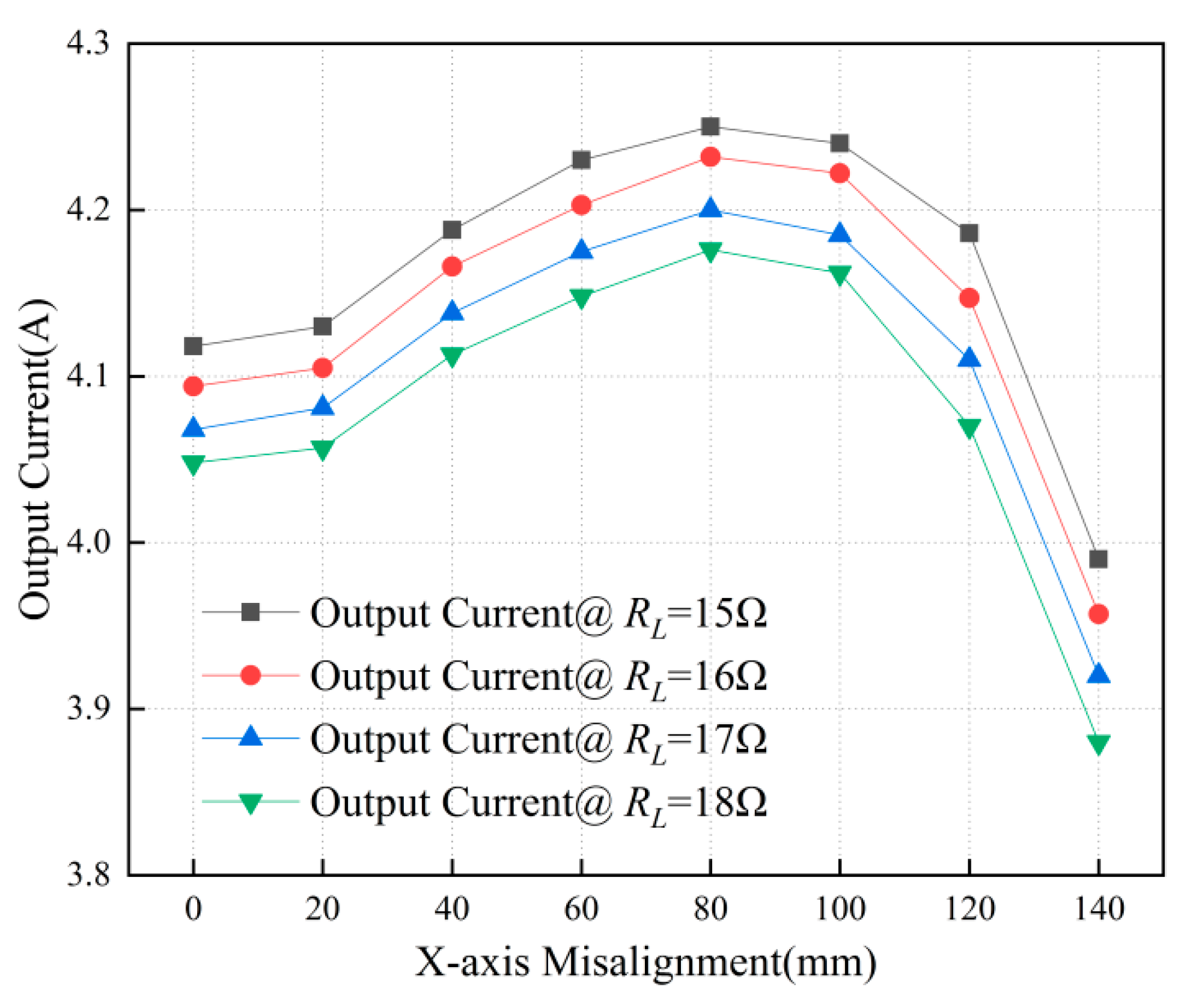
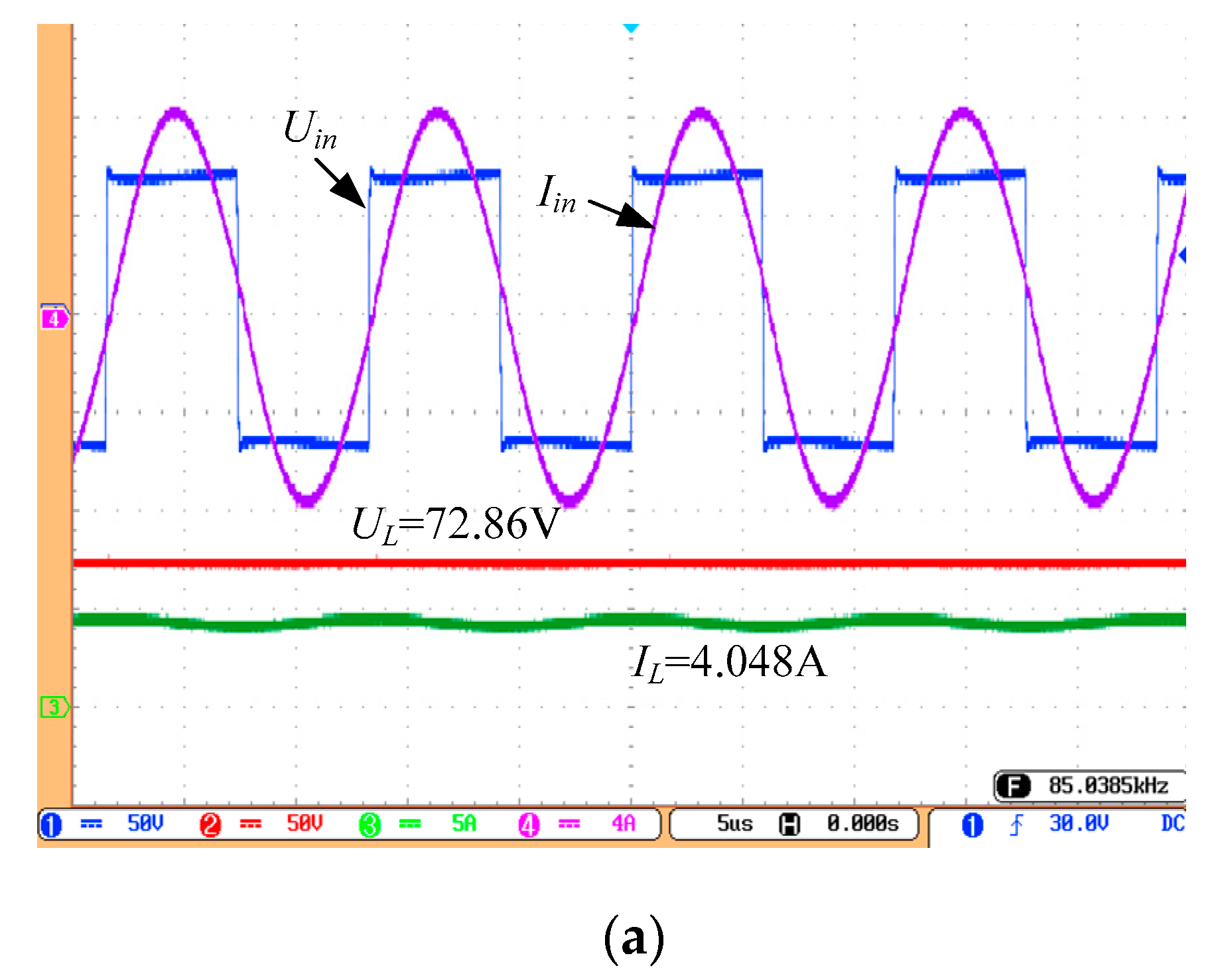
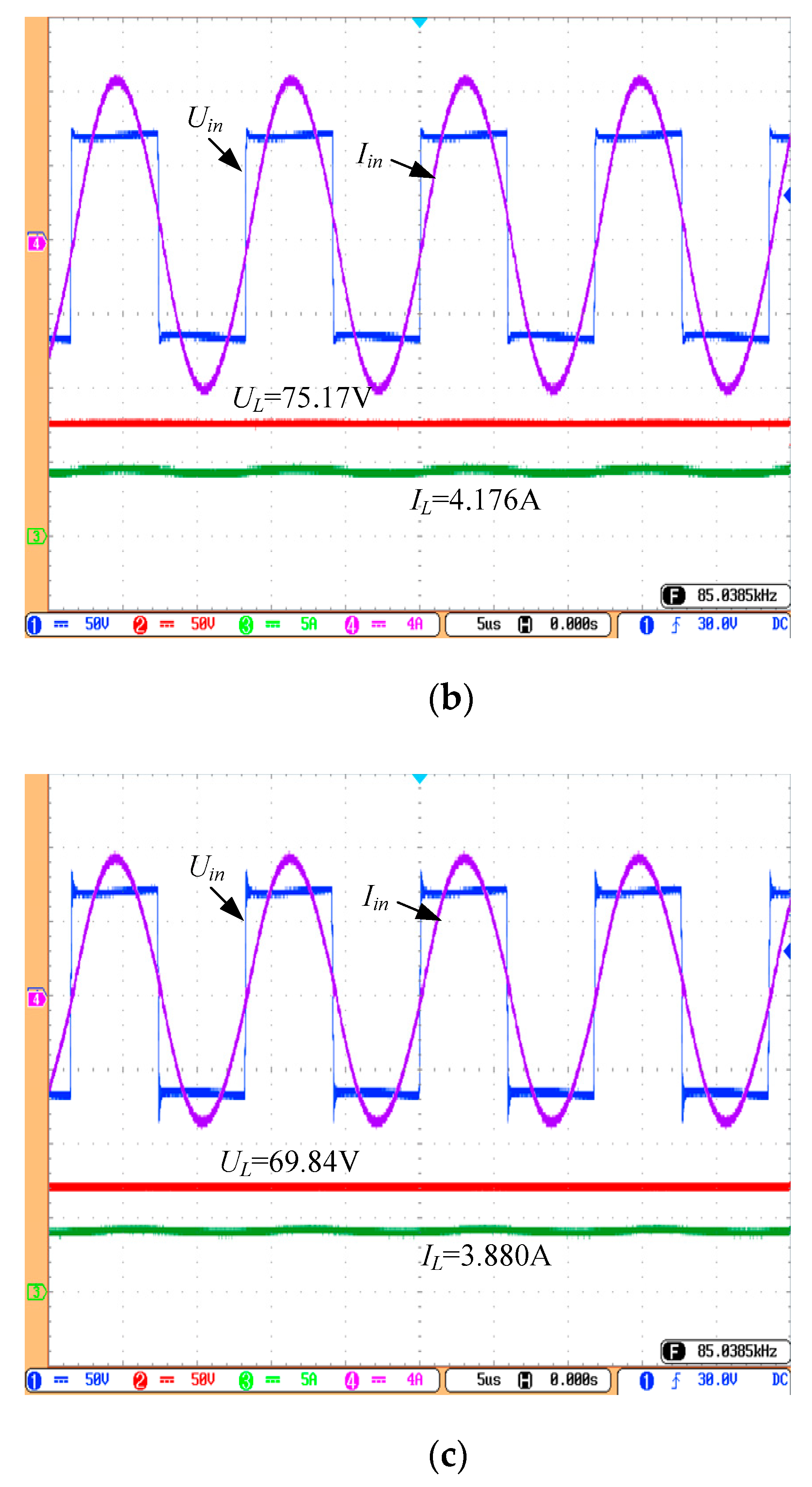
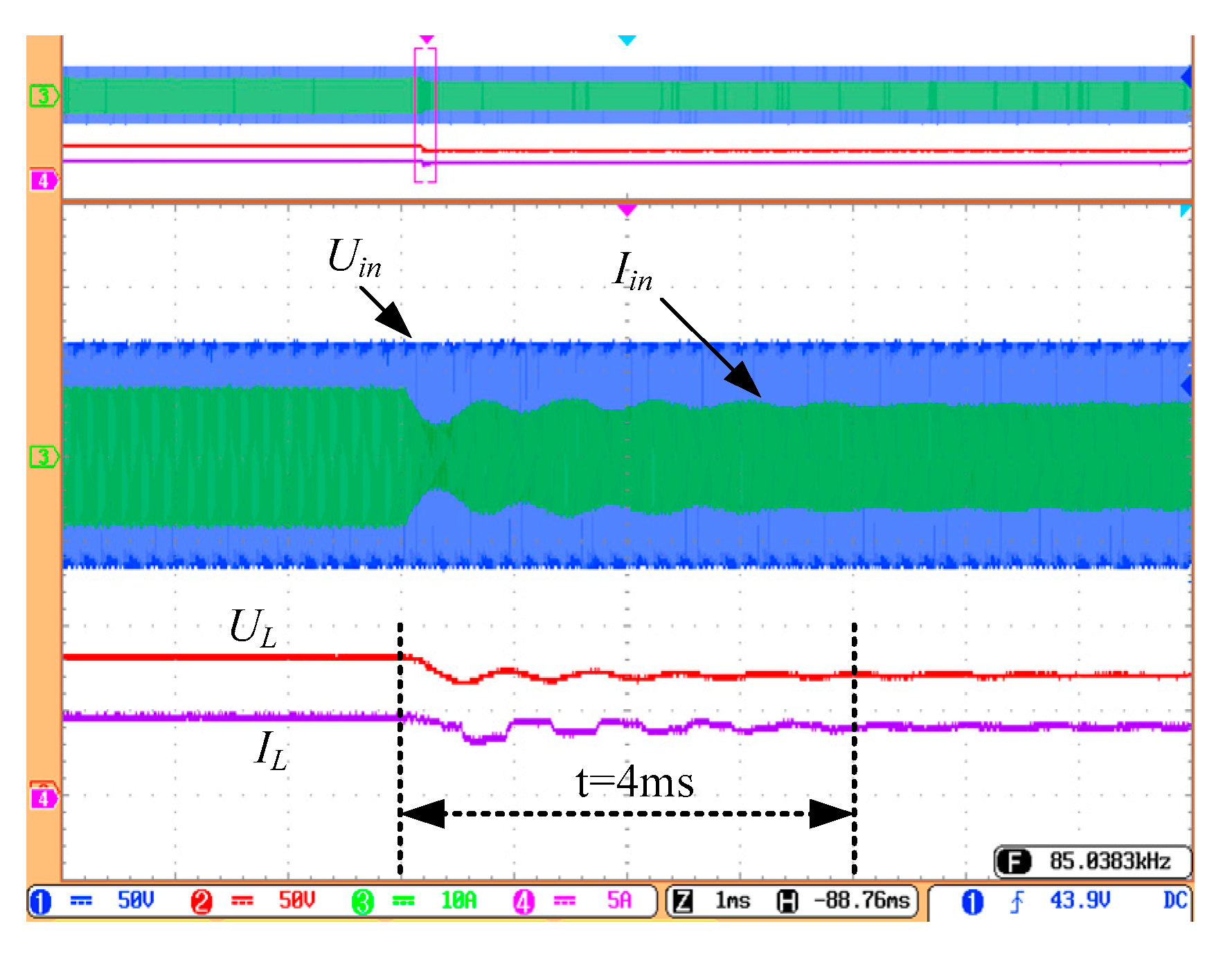
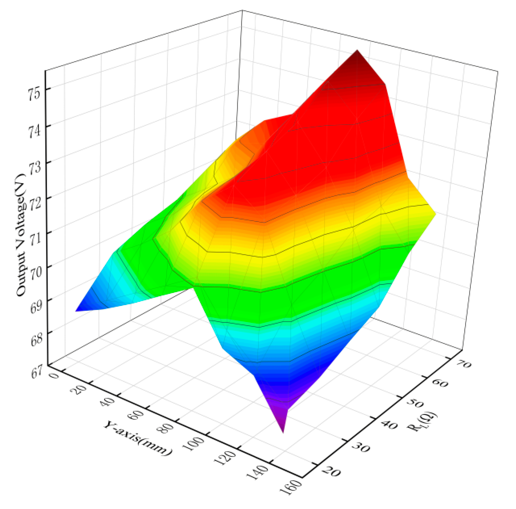
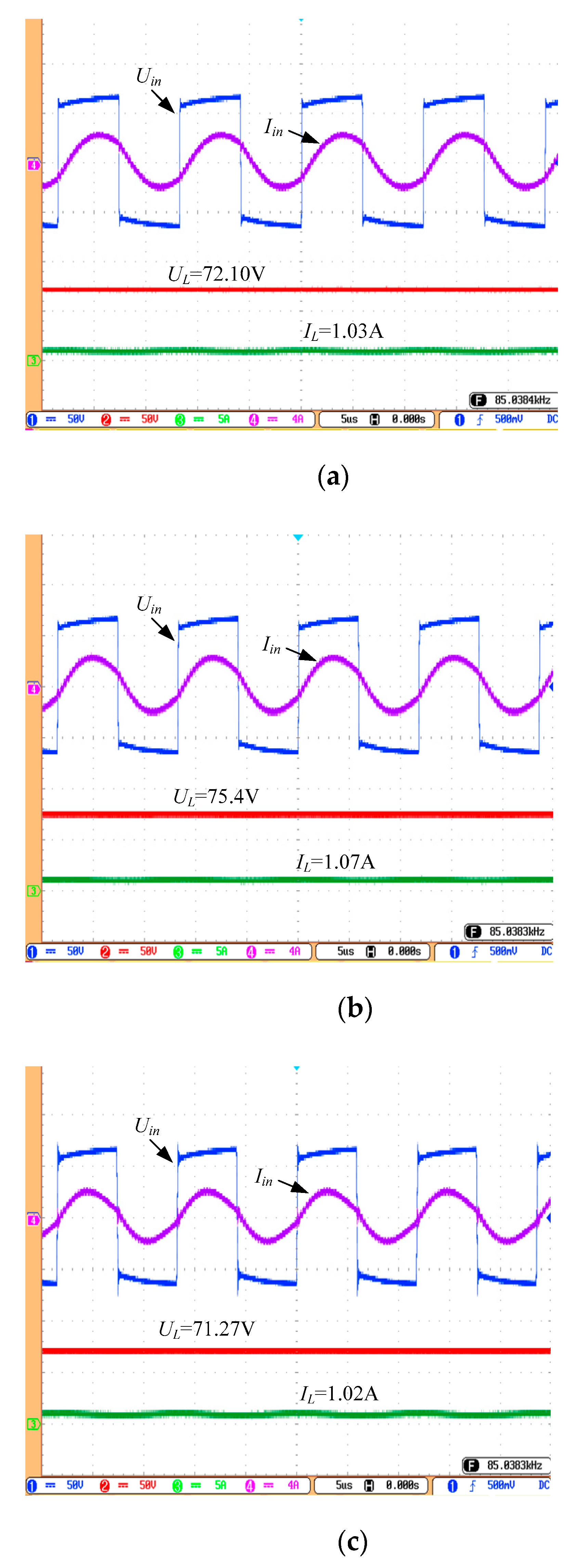
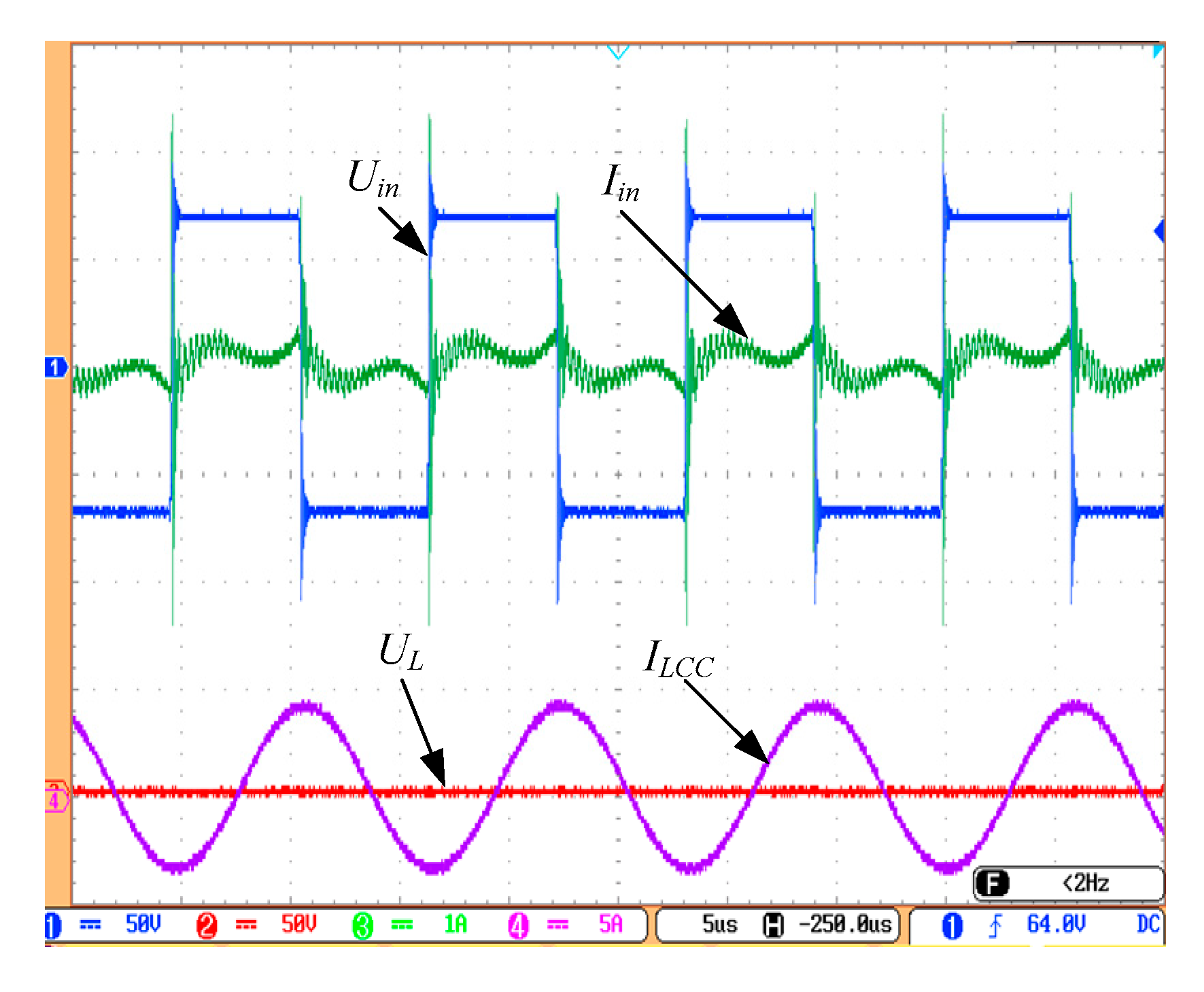
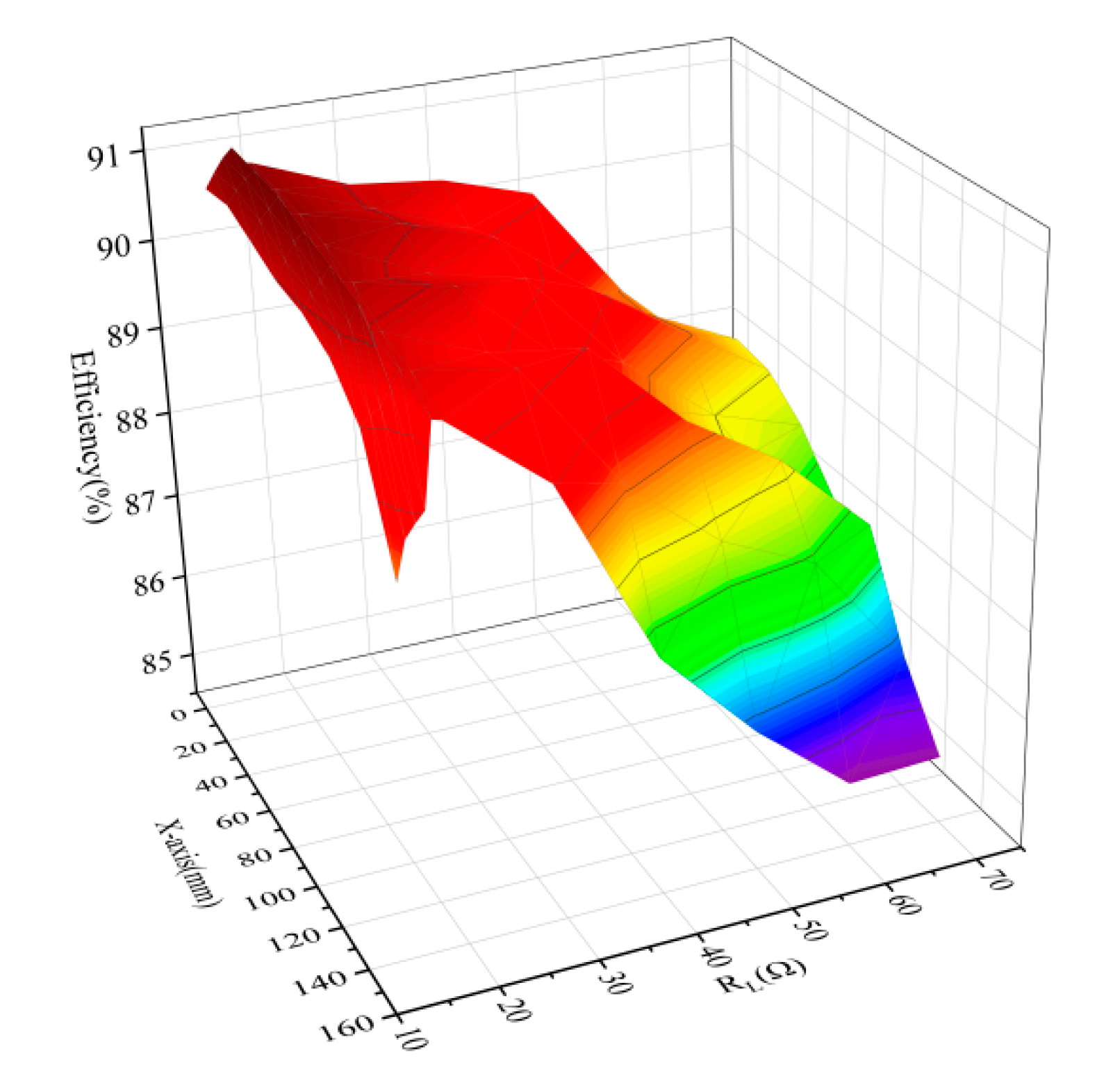
4.1. CC Output Performance of the System

Figure 11 plots the measured output current varying with the loads and X-axis misalignment. Within 140 mm X-axis misalignment, the output current of the system is between 3.85 and 4.25 A, meeting the requirement of 5% deviation. Under the same misalignment condition, the output current of 15 Ω is largest, and the output current of 18 Ω slightly decreased. If the load becomes lighter, the current fluctuation will exceed the limitation of 5%. In addition, the system output current is minimum when the receiving coil is offset to 140 mm. Additionally, it is clearly found that the load current increases first and then decreases with the increase of the offset distance, which is beneficial to improve the anti-offset ability of the system.
As is shown in Figure 12, the output voltage Uin and the output current Iin of the inverter are almost in the same phase, which indicates that near zero reactive power is achieved. Additionally, the output voltage UL and output current IL, indicate that the system can achieve a relative constant current output within 50% X-axis misalignment.
The function switches consist of two anti-series-connected MOSFETs, which are shown in Figure 13. When the S1 switch is ON and the S2 switch is OFF, the system works in CC mode. Otherwise, the system works in CV mode. Figure 14 shows the sudden transient waveforms. There are some oscillations when the charging mode changes from CC to CV output. In CC mode, the output current is around 4 A, and the output voltage is about 72 V in CV mode. In addition, the system only takes about 4 ms to reach the new steady state.

4.2. CV Output Performance of the System

As is shown in Figure 15, the output voltage of the system is between 68.5 and 75.5 V within 140 mm X-axis misalignment, meeting the requirement of 5% deviation, when the loads vary from 19 to 70 Ω. In addition, if the load becomes lighter, the voltage fluctuation will exceed the limitation of 5%. Additionally, the system output voltage climbs to the peak when the receiving coil is offset to 80 mm, which is consistent with the trend of the output current.
Figure 16 shows that there is a small phase angle between the voltage and the current of the inverter, which indicates that ZVS is achieved within 50% X-axis misalignment. Additionally, the output voltage UL and output current IL indicate that the system can achieve relative constant voltage output within 50% X-axis misalignment.
Figure 17 shows the experiment waveforms when the pick-up sides moved far away. The output voltage of the system is zero, and the current of the inverter is near zero, which indicates that the proposed system can work without the pick-up sides, and increase the stability of the system without any extra controllers.
Figure 18 shows that the efficiency in CC mode is between 91.0% and 89.2%, while the efficiency in CV mode is between 90.5% and 85.2%. In addition, the efficiency drops with the increase of the X-axis misalignment, because the increasing current flows into the L1 coil, resulting in increasing corresponding conductance loss.

4.3. Comparison with Other Methods

The performance of the proposed approach was compared with methods using control schemes and compensation topologies, as listed in Table 2. Compared with methods using control schemes, such as [14,16,17], the proposed WPT system can realize CC-CV output without an additional control scheme. Compared with methods using variable compensation topologies, such as [19,20], the proposed WPT system can both realize CC-CV output and misalignment tolerance. Among [31,32,33], the hybrid topologies are employed to improve misalignment tolerance. However, they can only achieve CC or CV output. Compared with [34], the proposed WPT system uses fewer components, and can operate without the pickup side, which improves the reliability of the system. Therefore, the proposed WPT system is superior to the other approaches in terms of CC and CV output, misalignment tolerance, and the ability of operating without a pickup pad.

5. Conclusions

In this article, a series hybrid wireless charging system with an active adjustable circuitry is proposed to obtain CC and CV outputs with high misalignment tolerance. The system is combined with series LCC-S topology in the primary side and pick-up side and T-type configurable topology, which can limit the current of the inverter without an extra controller when the pick-up pad moves out of the operating region. Besides, the function switch is employed to transfer CC output to CV output without complicated control schemes. Moreover, a parameter optimization design method is presented to provide high misalignment tolerance. The experimental results demonstrate that the system can maintain the output current fluctuation to be less than 5% with the load varying from 15 to 18 Ω, and the output voltage fluctuation less than 5% with the load varying from 19 to 70 Ω, when the pick-up pads are within 50% misalignment. The results demonstrate the theoretical analysis, and indicate that the series hybrid and configurable wireless charging system offers a reliable solution to wireless EV charging applications.

Author Contributions

Conceptualization, Z.-W.G.; Data curation, J.-G.L.; Formal analysis, Z.-W.G.; Funding acquisition, Z.-W.G.; Investigation, X.-Q.T.; Methodology, J.-G.L.; Project ministration, J.-G.L.; Resources, J.-G.L. and X.-Q.T.; Software, Z.-W.G.; Supervision, J.-G.L.; Validation, J.-G.L.; Visualization, Z.-W.G.; Writing—original draft, Z.-W.G. and J.-G.L.; Writing—review & editing, J.-G.L. and X.-Q.T. All authors have read and agreed to the published version of the manuscript.

Funding

This research was funded by Project number: 2020KJRC0035 from Xi’an Science and Technology Bureau, (China).

Institutional Review Board Statement

Not applicable.

Informed Consent Statement

Not applicable.

Data Availability Statement

Not applicable.

Acknowledgments

This work was supported by the Key Research Project of Shaanxi Province of China under Grant 2021KWZ-20.

Conflicts of Interest

The authors declare no conflict of interest.

References

  1. Ke, G.; Chen, Q.; Gao, W. Research on IPT Resonant Converters with High Misalignment Tolerance Using Multicoil Receiver Set. IEEE Trans. Power Electron. 2020, 35, 3697–3712. [Google Scholar] [CrossRef]
  2. Kan, T.; Mai, R.; Mercier, P.-P.; Mi, C.-C. Design and Analysis of a Three-Phase Wireless Charging System for Lightweight Autonomous. IEEE Trans. Power Electron. 2018, 33, 6622–6632. [Google Scholar] [CrossRef]
  3. Wang, X.; Xu, J.; Leng, M. Individually Regulated Dual—Output IPT System Based on Current—Mode Switching Cells. IEEE Trans. Ind. Electron. 2021, 68, 12930–12934. [Google Scholar] [CrossRef]
  4. Dai, X.; Li, X.; Hu, A.-P. Maximum Efficiency Tracking for Wireless Power Transfer Systems with Dynamic Coupling Coefficient Estimation. IEEE Trans. Power Electron. 2018, 33, 5005–5015. [Google Scholar] [CrossRef]
  5. Choi, S.-Y.; Gu, B.-W.; Jeong, S.Y. Advances in Wireless Power Transfer Systems for Roadway-Powered Electric Vehicles. IEEE Trans. Power Electron. 2015, 3, 18–36. [Google Scholar] [CrossRef]
  6. Lu, J.; Zhu, G.; Member, S.; Lin, D. Load-Independent Voltage and Current Transfer Characteristics of High-Order Resonant Network in IPT System. IEEE J. Emerg. Sel. Top. Power Electron. 2019, 7, 422–436. [Google Scholar] [CrossRef]
  7. Madawala, U.-K.; Thrimawithana, D.-J. A Bidirectional Inductive Power Interface for Electric Vehicles in V2G Systems. IEEE Trans. Ind. Electron. 2011, 58, 4789–4796. [Google Scholar] [CrossRef]
  8. Mi, C.; Buja, G.; Choi, S.; Su, Y. Modern Advances in Wireless Power Transfer Systems for Roadway Powered Electric Vehicles. IEEE Trans. Ind. Electron. 2016, 63, 6533–6545. [Google Scholar] [CrossRef]
  9. Su, Y.; Chen, L.; Wu, X. Load and Mutual Inductance Identification from the Primary Side of Inductive Power Transfer System with Parallel-Tuned Secondary Power Pickup. IEEE Trans. Power Electron. 2018, 33, 9952–9962. [Google Scholar] [CrossRef]
  10. Thrimawithana, D.-J.; Madawala, U.-K.; Neath, M. A Synchronization Technique for Bidirectional IPT Systems. IEEE Trans. Ind. Electron. 2013, 60, 301–309. [Google Scholar] [CrossRef]
  11. Vu, V.-B.; Phan, V.-T.; Dahidah, M. Multiple Output Inductive Charger for Electric Vehicles. IEEE Trans. Power Electron. 2019, 34, 7350–7368. [Google Scholar] [CrossRef] [Green Version]
  12. Weerasinghe, S.; Madawala, U.-K.; Thrimawithana, D.-J. A Matrix Converter-Based Bidirectional Contactless Grid Interface. IEEE Trans. Power Electron. 2017, 32, 1755–1766. [Google Scholar] [CrossRef]
  13. Dai, X.; Li, X.; Li, Y.; Hu, A.-P. Impedance-Matching Range Extension Method for Maximum Power Transfer Tracking in IPT System. IEEE Trans. Power Electron. 2018, 33, 4419–4428. [Google Scholar] [CrossRef]
  14. Li, Z.; Zhu, C.; Jiang, J.; Song, K.; Wei, G. A 3-kW Wireless Power Transfer System for Sightseeing Car Supercapacitor Charge. IEEE Trans. Power Electron. 2017, 32, 3301–3316. [Google Scholar] [CrossRef]
  15. Yao, Y.; Wang, Y.; Liu, X. Analysis Design and Optimization of LC/S Compensation Topology with Excellent Load-Independent Voltage Output for Inductive Power Transfer. IEEE Trans. Transp. Electrif. 2018, 4, 767–777. [Google Scholar] [CrossRef]
  16. Song, K.; Li, Z.; Jiang, J. Constant Current/Voltage Charging Operation for Series—Series and Series—Parallel Compensated Wireless Power Transfer Systems Employing Primary-Side Controller. IEEE Trans. Power Electron. 2018, 33, 8065–8080. [Google Scholar] [CrossRef]
  17. Li, Z.; Song, K.; Jiang, J.; Zhu, C. Constant Current Charging and Maximum Efficiency Tracking Control Scheme for Supercapacitor. IEEE Trans. Power Electron. 2018, 33, 9088–9100. [Google Scholar] [CrossRef]
  18. Wang, C.; Covic, G.-A.; Stielau, O.-H. Power Transfer Capability and Bifurcation Phenomena of Loosely Coupled Inductive Power Transfer Systems. IEEE Trans. Ind. Electron. 2004, 51, 148–157. [Google Scholar] [CrossRef]
  19. Li, Y.; Hu, J.; Chen, F.; Liu, S.; Yan, Z.; He, Z. A New-Variable-Coil-Structure-Based IPT System with Load-Independent Constant Output Current or Voltage for Charging Electric Bicycles. IEEE Trans. Power Electron. 2018, 33, 8226–8230. [Google Scholar] [CrossRef]
  20. Chen, Y.; Li, M.; Yang, B.; Chen, S.; Li, Q. Variable-Parameter T-Circuit Based IPT System Charging Battery with Constant Current or Constant Voltage Output. IEEE Trans. Power Electron. 2020, 35, 1672–1684. [Google Scholar] [CrossRef]
  21. Mai, R.; Chen, Y.; Li, Y.; Zhang, Y. Inductive Power Transfer for Massive Electric Bicycles Charging Based on Hybrid Topology Switching with a Single Inverter. IEEE Trans. Power Electron. 2017, 32, 5897–5906. [Google Scholar] [CrossRef]
  22. Wang, D.; Qu, X.; Yao, Y.; Yang, P. Hybrid Inductive-Power-Transfer Battery Chargers for Electric Vehicle Onboard Charging with Configurable Charging Profile. IEEE Trans. Intell Transp. 2021, 22, 592–599. [Google Scholar] [CrossRef]
  23. Liu, Y.; Mai, R.; Yue, P.; Li, Y.; He, Z. Efficiency Optimization for Wireless Dynamic Charging System with Overlapped DD Coil Arrays. IEEE Trans. Power Electron. 2018, 33, 2832–2846. [Google Scholar] [CrossRef]
  24. Miller, J.-M.; Onar, O.-C.; Chinthavali, M. Primary-Side Power Flow Control of Wireless Power Transfer for Electric Vehicle Charging. IEEE J. Emerg. Sel. Top. Power Electron. 2015, 3, 147–162. [Google Scholar] [CrossRef]
  25. Park, C.; Lee, S.; Jeong, S.-Y.; Cho, G.; Rim, C.-T. Uniform Power I-Type Inductive Power Transfer System with DQ -Power Supply Rails for On-Line Electric Vehicles. IEEE Trans. Power Electron. 2015, 30, 6446–6455. [Google Scholar] [CrossRef]
  26. Zhao, J.-I.; Zhang, N.-J.; Zhu, Y. A Flexible Wireless Power Transfer System with Switch Controlled Capacitor. IEEE Access. 2019, 7, 106873–106881. [Google Scholar] [CrossRef]
  27. Zhang, Z.; Zhang, B. Angular-Misalignment Insensitive Omnidirectional Wireless Power Transfer. IEEE Trans. Ind. Electron. 2020, 67, 2755–2764. [Google Scholar] [CrossRef]
  28. Kim, S.; Covic, G.-A.; Boys, J.-T. Tripolar Pad for Inductive Power Transfer Systems for EV Charging. IEEE Trans. Power Electron. 2017, 32, 5045–5057. [Google Scholar] [CrossRef]
  29. Chen, Y.; Yang, B.; Zhou, X.; Li, Q.; He, Z. A Hybrid Inductive Power Transfer System with Misalignment Tolerance Using Quadruple-D Quadrature Pads. IEEE Trans. Ind. Electron. 2020, 35, 6039–6049. [Google Scholar] [CrossRef]
  30. Yao, Y.; Wang, Y.; Liu, X.; Pei, Y. A Novel Unsymmetrical Coupling Structure Based on Concentrated Magnetic Flux for. IEEE Trans. Power Electron. 2019, 34, 3110–3123. [Google Scholar] [CrossRef]
  31. Zhao, L.; Thrimawithana, D.-J.; Madawala, U.-K. Hybrid Bidirectional Wireless EV Charging System Tolerant to Pad Misalignment. IEEE Trans. Ind. Electron. 2017, 64, 7079–7086. [Google Scholar] [CrossRef]
  32. Zhao, L.; Member, S.; Thrimawithana, D.-J.; Member, S.; Madawala, U.-K.; Hu, A.-P.; Member, S.; Mi, C.-C. A Misalignment-Tolerant Series-Hybrid Wireless EV Charging System with Integrated Magnetics. IEEE Trans. Power Electron. 2019, 34, 1276–1285. [Google Scholar] [CrossRef]
  33. Qu, X.; Yao, Y.; Wang, D.; Wong, S.; Tse, C.-K. A Family of Hybrid IPT Topologies with Near Load-Independent Output and High Tolerance to Pad Misalignment. IEEE Trans. Ind. Electron. 2020, 35, 6867–6877. [Google Scholar] [CrossRef]
  34. Chen, Y.; Yang, B.; Kou, Z.; He, Z. Hybrid and Reconfigurable IPT Systems with High-Misalignment Tolerance for Constant-Current and Constant-Voltage Battery Charging. IEEE Trans. Power Electron. 2018, 33, 8259–8269. [Google Scholar] [CrossRef]
Figure 1. Series hybrid and configurable topology.
Energies 14 07594 g001
Figure 2. Equivalent circuit of the series hybrid topology.
Energies 14 07594 g002
Figure 3. Equivalent circuit of the configurable topology.
Energies 14 07594 g003
Figure 4. Equivalent circuit of the configurable topology with CV output.
Energies 14 07594 g004
Figure 5. Simplified circuit model using the Thevenin equivalent circuit.
Energies 14 07594 g005
Figure 6. Equivalent circuit with the series hybrid and configurable topology.
Energies 14 07594 g006
Figure 7. Magnetic coupler using the DDQ structure.
Energies 14 07594 g007
Figure 8. Measured mutual inductances misalignments: (a) X-axis misalignment; (b) Y-axis misalignment; (c) Z-axis misalignment.
Energies 14 07594 g008aEnergies 14 07594 g008b
Figure 9. The function of I3 and M12 in X-axis misalignment.
Energies 14 07594 g009
Figure 10. Experimental setup of the series hybrid and configurable wireless charging system.
Energies 14 07594 g010
Figure 11. Measured output current varying with the RL loads and X-axis misalignment.
Energies 14 07594 g011
Figure 12. Experimental waveforms of Uin, Iin, UL, IL with RL = 18 Ω: (a) at a well-aligned position; (b) at the 80 mm X-axis misaligned position; and (c) at the 140 mm X-axis misaligned position. (Uin: 50 V/div; Iin: 4 A/div; UL: 50 V/div; IL: 5 A/div; t: 5 us).
Energies 14 07594 g012aEnergies 14 07594 g012b
Figure 13. The function switch with two anti-series-connected MOSFETs.
Energies 14 07594 g013
Figure 14. Experimental waveforms of Uin, Iin, UL, IL with RL = 19 Ω from the CC mode to the CV mode. (Uin: 50 V/div; Iin: 4 A/div; UL: 50 V/div; IL: 5 A/div; t: 1 ms).
Energies 14 07594 g014
Figure 15. Measured output voltage varying with RL loads and X-axis misalignment.
Energies 14 07594 g015
Figure 16. Experimental waveforms of Uin, Iin, UL, IL with RL = 70 Ω in the CV mode: (a) at the well-aligned position; (b) at the 80 mm X-axis misaligned position; and (c) at the 140 mm X-axis misaligned position. (Uin: 50 V/div; Iin: 4 A/div; UL: 50 V/div; IL: 5 A/div; t: 5 us).
Energies 14 07594 g016
Figure 17. Experimental waveforms of Uin, Iin, UL, ILCC when the pick-up sides moved far away (mutual inductance M12 and M34 are zero) (Uin: 50 V/div; Iin: 1 A/div; UL: 50 V/div; ILCC: 5 A/div; t: 5 us).
Energies 14 07594 g017
Figure 18. Measured efficiency curves varying with RL loads and X-axis misalignment.
Energies 14 07594 g018
Table 1. Configurations of the WPT system.
ParameterValueParameterValue
f85 kHzC126.6 nF
L1150.1 uHC2220.1 nF
L2149.8 uHC322.5 nF
L3156.1 uHC422.5 nF
L4156.0 uHC526.5 nF
CE25.0 nFE70 V
C0220.2 nF
Table 2. Comparison with methods using control schemes and compensation topologies.
Proposed inRef. [14]Ref. [16]Ref. [17]Ref. [19]Ref. [20]Ref. [31]Ref. [32]Ref. [33]Ref. [34]This Work
Control schemeYesYesYesNoNoNoNoNoNoNo
Number of Component2 + dc-dc
converter
22 + semi-active
rectifier
458681211
k0.20.20.150.220.170.18–0.300.15–0.350.08–0.160.1–0.20.1–0.2
Max. power3 kW103 W66 W105 W400 W3.3 kW3.3 kW3.5 kW1 kW280 W
CC or CVCCCC-CVCCCC-CVCC-CVCCCCCVCC-CVCC-CV
Peak efficiency88%75%86%91%94%91%94%93%94%91%
Frequency (kHz)85.585.585.5500858585858585
Misalignment toleranceNoNoNoNoNoYesYesYesYesYes
Wireless communicationYesNoNoYesYesNoNoNoNoNo
Operate without pickup pad\\\\\NoYesYesNoYes
Publisher’s Note: MDPI stays neutral with regard to jurisdictional claims in published maps and institutional affiliations.

