Article

Amorphous Silicon Thin Film Deposition for Poly-Si/SiO2 Contact Cells to Minimize Parasitic Absorption in the Near-Infrared Region

1
Department of Materials Science and Engineering, Korea University, Seoul 02841, Korea
2
Photovoltaics Laboratory, Korea Institute of Energy Research, Daejeon 34129, Korea
3
Meiji Renewable Energy Laboratory, Meiji University, 1-1-1 Higashimita, Tama-ku, Kawasaki 214-8571, Japan
4
Hanwha Q CELLS GmbH, Sonnenallee 17-21, Bitterfeld-Wolfen OT Thalheim, 06766 Bitterfeld-Wolfen, Germany
5
KU-KIST Graduate School of Energy and Environment, Green School, Korea University, 145, Anam-ro, Seongbuk-gu, Seoul 02841, Korea
*
Authors to whom correspondence should be addressed.
Submission received: 26 October 2021 / Revised: 23 November 2021 / Accepted: 29 November 2021 / Published: 7 December 2021
(This article belongs to the Special Issue Recent Development of Silicon Solar Cells)

Abstract

:
Tunnel oxide passivated contact (TOPCon) solar cells are key emerging devices in the commercial silicon-solar-cell sector. It is essential to have a suitable bottom cell in perovskite/silicon tandem solar cells for commercial use, given that good candidates boost efficiency through increased voltage. This is due to low recombination loss through the use of polysilicon and tunneling oxides. Here, a thin amorphous silicon layer is proposed to reduce parasitic absorption in the near-infrared region (NIR) in TOPCon solar cells, when used as the bottom cell of a tandem solar-cell system. Lifetime measurements and optical microscopy (OM) revealed that modifying both the timing and temperature of the annealing step to crystalize amorphous silicon to polysilicon can improve solar cell performance. For tandem cell applications, absorption in the NIR was compared using a semitransparent perovskite cell as a filter. Taken together, we confirmed the positive results of thin poly-Si, and expect that this will improve the application of perovskite/silicon tandem solar cells.

1. Introduction

The commercial solar-cell market is largely based on silicon wafers, and silicon accounts for approximately 80% of annual production in the photovoltaic market [1]. However, as crystalline silicon, single-junction solar cells are approaching the 29.4% limit of power convention efficiency (PCE) [2], many researchers and companies are beginning to develop silicon-based tandem devices as next-generation commercial solar cells to achieve better energy yield across the solar spectrum, and to reach an improved theoretical efficiency potential [3,4]. Among these emerging devices, perovskite/silicon tandem solar cells represent an attractive technology for commercial use due to advantages of perovskite, such as wide bandgap tunability, relatively simple design, and low cost. Together, these features enable a much-improved theorical efficiency potential of approximately 46% [5,6].
For commercial application of tandem solar cells, silicon solar cells should enable the manufacturing of inexpensive, mass-produced cells that tolerate high temperatures [7]. The silicon solar-cell technology that has garnered the most attention is the carrier-selective contact structure, using a thin tunnel oxide and polysilicon [8,9]. This structure was first unveiled by Fraunhofer ISE as a tunnel oxide passivated contact (TOPCon) structure, and achieved 26.0% conversion efficiency over an area of 4 cm2 by incorporating a phosphorus-doped polysilicon layer and a passivated, thin silicon oxide (SiO2) film on the silicon surface to selectively transfer electrons [10]. TOPCon solar cells, which exhibit high efficiency with a simple structure, are gradually being applied to the solar industry, and have been highlighted as suitable bottom cells for next-generation perovskite/silicon tandem solar cells [11,12].
For TOPCon structures with high-quality passivation characteristics, it is important to optimize the SiO2/poly-Si contacts deposited on the rear side of the solar cell [13]. However, because of the large absorption coefficient of polysilicon at long wavelengths [14], if the polysilicon layer is thick, parasitic absorption of long-wavelength light (in the near-infrared region (NIR)) increases [15], and limits the current of both the silicon and perovskite/silicon devices. Reducing this parasitic absorption in the NIR is particularly important in a tandem device because the silicon cell absorbs the light passing through the perovskite top cell [16,17].
In this study, thin amorphous silicon was deposited through plasma-enhanced chemical vapor deposition (PECVD) to reduce parasitic absorption of polysilicon on the back side of the cell, and a TOPCon structure was fabricated by crystallizing the amorphous film into poly-Si through an additional high-temperature heat treatment. With PECVD, high current can be obtained, and the heat treatment temperature of polysilicon can be lowered [18]. In addition, single-sided deposition simplifies solar cell manufacturing [19]. To reduce the hydrogen blistering that occurs during this process [20], a step-by-step heat treatment process was applied. Furthermore, the feasibility of perovskite/silicon tandem solar cells was confirmed by measuring the external quantum efficiency (EQE) of the bottom cell with light transmitted through the perovskite top cell.

2. Materials and Methods

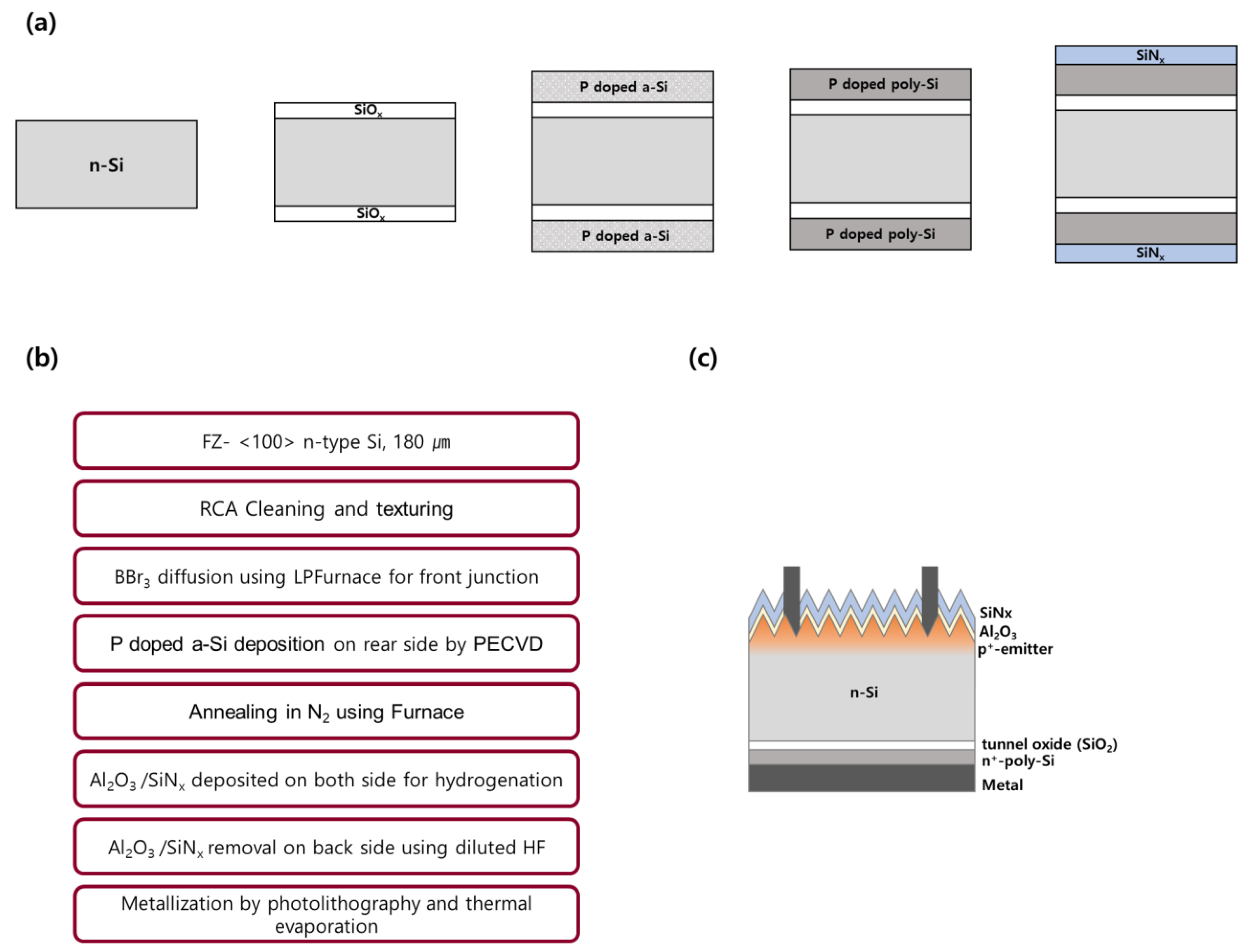
2.1. Sample Preparation

The silicon wafers used in this study have a designated illumination area of 2 × 2 cm2. Specifically, phosphorus-doped, float-zone, 3-inch, polished (100) n-type silicon wafers, with a resistivity of approximately 2 Ω·cm and a thickness of 300 μm, were prepared. All samples were cleaned using standard Radio Corporation of America (RCA) solutions and dipped in hydrofluoric acid to remove the native oxide.

2.2. Passivation Test

To measure the implied open-circuit voltage for passivation quality, samples were prepared in a double-sided symmetrical structure. A thin silicon oxide layer for tunneling oxide with a thickness of 1–1.5 nm was grown on the silicon surface by dipping the wafer into an H2O2 solution at 80 °C for 10 min. Next, annealing was performed at 550 °C for 30 min by a tube furnace under ambient N2. After tunnel oxide formation, a phosphorus-doped, amorphous silicon thin film was deposited with H2, SiH4, and PH3 through PECVD, and then annealed in a tube furnace under various conditions. This sample was passivated with 80 nm SiNx via PECVD. For the hydrogenation process, N2 annealing was performed at 550 °C for 15 min by a rapid thermal process. A schematic diagram of the sample preparation process is shown in Figure 1a.

2.3. Cell Fabrication

The front side of the silicon featured an alkali-etched, random pyramidal texture, which was etched at 80 °C for 30 min using a DI:KOH:additive solution to form a random pyramidal texture. A boron-doped p+ emitter was formed by BBr3 diffusion at 1010 °C in a liquid propane furnace (centrotherm). The sheet resistance showed characteristics of 100–120 Ω/sq. After removing the borosilicate glass using a dilute hydrofluoric acid (DHF) solution, poly-Si/SiOx stacks were formed under the conditions mentioned above (e.g., p+ emitter/Si/SiOx/n+ poly-Si). For hydrogenation, SiNx was deposited on the rear side by PECVD. Approximately 10 nm of Al2O3 was deposited on both sides at 220 °C using trimethyl aluminum (TMA, Al(CH3)3) and H2O as precursors by thermal atomic layer deposition (ALD). Then, the front side was additionally coated with SiNx as an antireflection layer (e.g., the structure contained SiNx/Al2O3/p+ emitter/Si/SiOx/n+ poly-Si/SiNx/Al2O3). After annealing to activate the Al2O3 surface passivation and hydrogenation, the SiNx/Al2O3 stack layer was etched in a DHF solution for full-area rear contact. The back electrode was formed by depositing 1 µm Ag using thermal evaporation and the front-side contact process was based on lithography and the lift-off technique. Forming gas annealing (FGA) was performed in the furnace at 350 °C for 30 min for metal contact. The cell fabrication process sequence is shown in Figure 1b, and the completed cell structure is shown in Figure 1c.

2.4. Semitransparent Perovskite Solar Cells

2.4.1. Materials

Acetone, ethanol, and isopropanol were purchased from Duksan (Gyeonggi-do, Korea). Chlorobenzene, dimethylformamide (DMF), dimethyl sulfoxide (DMSO), diethyl ether, 4-tert-butylpyridine (tBP), acetonitrile, and Bis(trifluoromethane)sulfonimide lithium salt (Li-TFSI) were purchased from Sigma-Aldrich. Next, 2,2′,7,7′-tetrakis-(N,N-di-4-methoxyphenylamino)-9,9′-spirobifluorene (spiro-OMeTAD) was purchased from Lumtec Technology Corp., New Taipei City, Taiwan. Methylammonium chloride (MACl), methylammonium bromide (MABr), and Formamidinium iodide (FAI) were purchased from Greatcell solar. Lead bromide (PbBr2) and lead iodide (PbI2) were purchased from TCI.

2.4.2. Methods

Fluorine tin oxide (FTO) substrates were sonicated with acetone, ethanol, and isopropanol for 10 min each. The surface of the cleaned substrate was treated with UV-Ozone for 30 min. The perovskite precursor solution (1.43 M FAI, 0.08 M MABr, 0.50 M MACl, 1.56 M PbI2, and 0.08 M PbBr2 in 8:1 DMF:DMSO by volume) was spin coated at 1000 rpm for 10 s and 5000 rpm for 40 s. During the spin coating, 700 μL of diethyl ether was dispensed after 30 s, and the sample was annealed at 120 °C for 20 min. The hole transfer layer (HTL) precursor solution consisted of 136.4 mg Spiro-OMeTAD, 39 μL tBP, 23 μL Li-TFSI solution (1.88 M in acetonitrile), and 1.5 mL chlorobenzene. The HTL precursor solution was spin-coated at 4000 rpm for 20 s. Next, the 15 nm MoOx buffer layer was deposited by thermal evaporation, and ITO was deposited on it by DC magnetron sputtering as a transparent electrode.

2.5. Characteristics

The current–voltage parameters of the photovoltaic cells were obtained using a Xe lamp solar simulator (WACOM WXS-155S10 class AAA) under standard testing conditions (in-house 1-sun, 25 °C). The passivation quality of the samples was determined by the quasi-steady-state photoconductance (QSSPC) measurement on a Sinton Lifetime Tester, model WCT-120. The quantum efficiency (QE) of solar cells was determined using an EQE system (PV measurement Inc., QEX7, WA 98281, USA) without any light/potential bias.

3. Results and Discussion

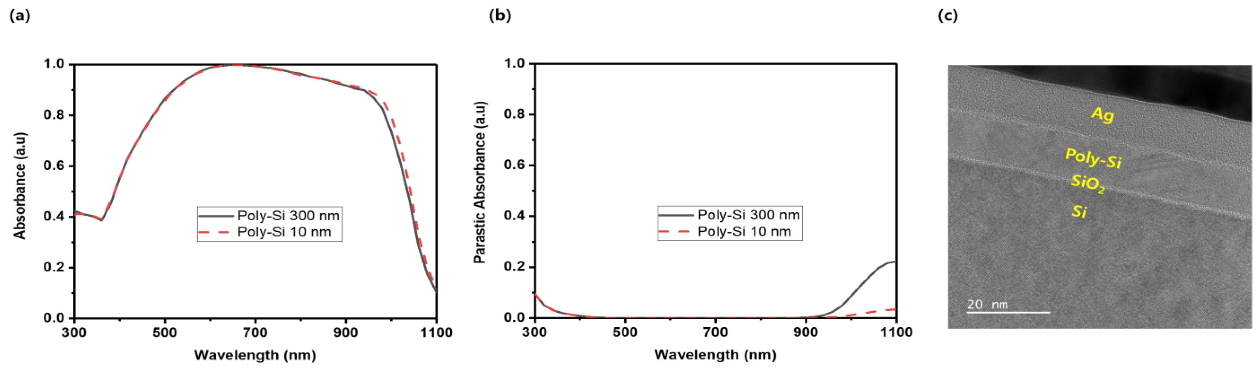
3.1. Optical Properties According to Poly-Si Thickness on the Rear Side
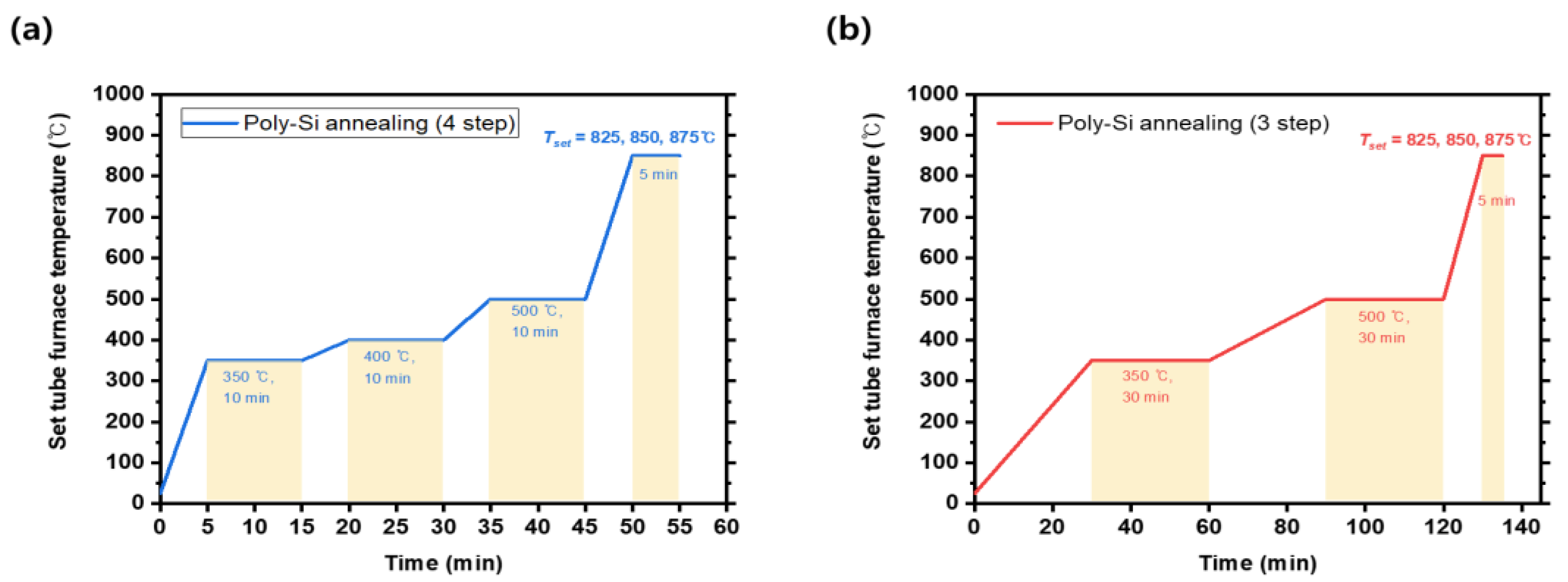
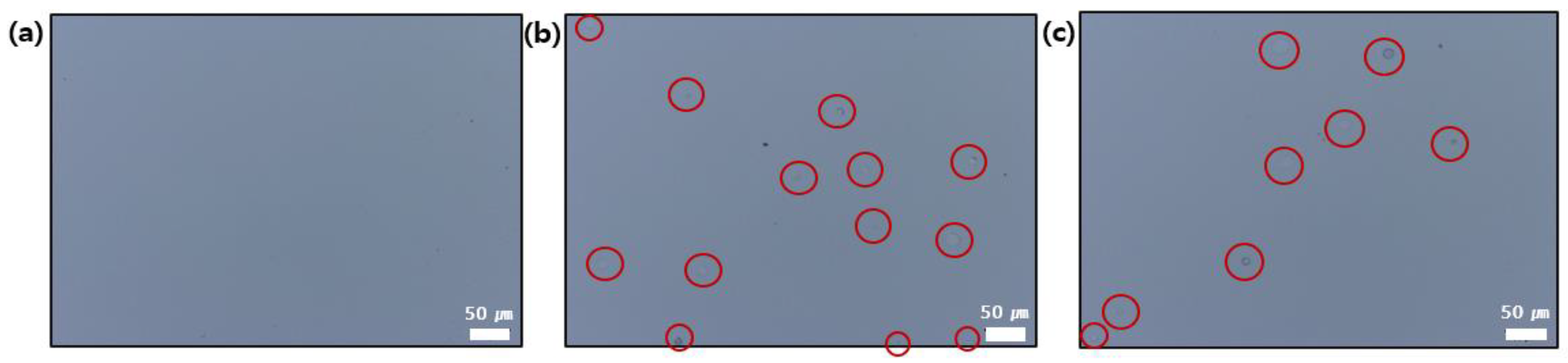
We investigated the optical properties according to the thickness of the poly-Si on the back of the TOPCon solar cells. To this end, we performed numerical optical simulations on TOPCon structures with various poly-Si thicknesses, using SunSolve Ray Tracer software in the PV light house. In this simulation, thickness was the only variable for poly-Si deposited with the same equipment, and the results are shown in Figure 2a. This simulation revealed the characteristics of absorption and parasitic absorption in the silicon wavelength region. As the poly-Si thickness increased, parasitic absorption appeared to increase in the wavelength range of 900 nm or more. There was a difference in the total light absorption at long wavelengths, due to the difference in poly-Si thickness. In a perovskite/silicon tandem device, the wavelength range of the Si bottom cell corresponds to approximately 730 nm and above (ideal perovskite bandgap is approximately 1.7 eV); therefore, the increase in light absorption of silicon cells at long wavelengths is crucial to ensure optimal performance of tandem solar cells. Based on the simulation, we analyzed the TOPCon cell with a poly-Si thickness of 10 nm. Figure 2b is a transmission electron microscopy image (TEM) of a poly-Si/SiOx cross-section from a TOPCon cell fabricated with 10 nm poly-Si, and the measurement result shows that poly-Si was deposited to a thickness of approximately 12 nm.

3.2. Annealing

To improve the conductivity of the carrier in the TOPCon structure, a process of converting the phosphorus-doped, amorphous silicon layer into polycrystalline silicon through a high-temperature heat treatment at approximately 800–900 °C is required. Through this process, it was confirmed that the passivation characteristics deteriorated, due to hydrogen blistering that occurred in the amorphous silicon film, based on the heat treatment profile. The bond between silicon and hydrogen begins to break at roughly 300 °C, and almost all hydrogen escapes at temperatures above 550 °C [21]. If this process proceeds quickly, blistering occurs in the polysilicon film. As the time of the heat treatment increased, at the temperature where the bond between silicon and hydrogen was broken during the dehydrogenation process, the resultant hydrogen blistering could be minimized, as shown in Figure 3.
In Figure 3a, peak-temperature annealing was performed following 5 min annealing steps at 350, 400, and 500 °C at the hydrogen-escape temperature. In Figure 3b, the peak-temperature annealing was performed after extending the heat treatment times from 350 °C to 500 °C. Blistering was minimized by increasing the annealing time in the hydrogen-escape temperature range, and was observed by optical microscopy, as shown in Figure 4. Figure 4a shows that blistering was not observed where amorphous silicon was deposited on the silicon surface; however, hydrogen blistering was observed in poly-Si that had undergone a high-temperature annealing process. In the case of the four-step annealing, Figure 4b shows hydrogen blistering that was not observable by the naked eye. However, in the case of the three-step annealing shown in Figure 4c, where the heat treatment time was increased in the temperature range where dehydrogenation occurs, hydrogen blistering was reduced by approximately 77% when compared to the 4-step annealing process shown in Figure 4b.
QSSPC measurements were performed on samples annealed with both the four- and three-step processes to confirm the effect of blistering on the passivation properties following heat treatment of amorphous silicon. As shown in Figure 5a, both four-step and three-step processes showed the highest implied open-circuit voltage (iVoc) of 716 and 727 mV, when the process was performed at a peak temperature of 850 °C for 5 min. The samples with extensive hydrogen blistering had low implied Voc values and high J0 values, as shown in Figure 5b. Samples with minimal hydrogen blistering exhibited uniform high quality passivation characteristics, with an implied Voc of more than 700 mV and a saturation current of less than 10 mA/cm2. In TOPCon structures deposited with 12 nm poly-Si, hydrogen blistering was minimized, and high implied Voc values and J0 values of 727 mV and 5, respectively, were obtained.
Solar cells were fabricated using the optimized TOPCon structure by heat treatment at 850 °C for 5 min on a 12 nm thin, amorphous silicon film, deposited through PECVD. Figure 6a shows the conversion efficiency of solar cells to which 12 nm thin n+ poly-Si was applied, compared with that of solar cells to which 300 nm thin n+ poly-Si was deposited by low-pressure chemical vapor deposition (LPCVD). The 300 nm poly-Si-deposited solar cell showed a conversion efficiency of 0.66 V, 40 mA/cm2, 0.75 FF, and 20%, whereas the 12 nm poly-Si-deposited solar cell (three-step annealing process) exhibited a conversion efficiency of 0.55 V, 38 mA/cm2, 0.6 FF, and 15%.
When the thin film was deposited through PECVD, we expected that the voltage would be reduced. This could be due to the metal being deposited at the location where hydrogen blistering occurred. Therefore, it showed that the series resistance increased due to the lifting of the metal and the direct contact on the Si interface, and the parallel resistance decreased as the non-uniform n+ polysilicon layer was formed [22]. In order to confirm the blistering phenomenon, Nemeth et al. confirmed that the device deteriorated as the metal penetrated the poly-Si through the PL images [23]. To address this issue, deposition conditions and the blistering phenomenon were optimized. The amount of blistering observed on the surface had been minimized by reducing the steps to reach high temperatures and by providing sufficient annealing time for each heat treatment section. Figure 6b compares the QE data of 12 nm and 300 nm TOPCon on solar cells. Although the overall QE value of 12 nm polysilicon was low, owing to Voc degradation due to hydrogen blistering, it was nevertheless confirmed that the QE val ue was high at wavelengths above 1000 nm. If the blistering problem of 12 nm polysilicon is fully optimized, it is expected that there will be an advantage in terms of Jsc.

3.3. Filtered Si Bottom Cell for Application of Perovskite/Silicon Tandem Solar Cells

To confirm these effects in a tandem device, a thin film with a perovskite cell structure was prepared as a filter. For measuring in the 4-terminal method, the filter was prepared in a semitransparent structure in which a transparent conductive oxide was deposited on the Spiro-OMeTAD. As shown in Figure 7a, the silicon cell was measured with transmitted light through a top cell with a 1.55 eV bandgap. Figure 7b shows the EQE results. The filtered poly-300 nm TOPCon cell showed a current of 11.6 mA/cm2, and the poly-12 nm TOPCon cell showed a current of 10.9 mA/cm2. The poly-12 nm cell exhibited a lower overall EQE than the 300 nm cell because recombination was increased by blistering, as shown above. However, the EQE value of the poly-12 nm cell was higher than that of the poly-300 nm cell at wavelengths ≥1000 nm, which was consistent with the simulation results. This result confirmed that the thinner the poly thickness, the higher the absorption at long wavelengths. However, because it still showed a low EQE value in regions other than the long wavelength, it became important to optimize a good quality, thin poly-Si thickness.
In future work, we plan to further improve the tandem cell design to not only solve the device degradation issue due to blistering in cells deposited with thin poly-Si, but also to maximize the use of long wavelengths when applied as a tandem device.

4. Conclusions

In this study, we investigated a method to improve the current in silicon solar cells of TOPCon structure and perovskite/silicon tandem solar cells. After confirming that the thickness of poly-Si influences solar cell optical properties, we confirmed this trend based on the heat treatment conditions using 12 nm poly-Si. This revealed that the cell showed reduced performance as the time to reach the heat treatment temperature was shortened, and this difference was found to be related to the number of blistering distributions developed in the poly-Si layer during the heat treatment process. Using a perovskite/silicon tandem cell, the characteristics of the lower cell were measured using the light transmitted through the upper cell. This confirmed that the thinner the poly-Si, the greater the light absorption in the long wavelength range of 1000 nm or greater. In the future, we plan to improve cell performance by reducing blistering and plan to fabricate monolithic perovskite/silicon tandem solar cells that can efficiently use light absorbed at long wavelengths.

Author Contributions

C.L. and J.H. contributed equally to this work. Conceptualization: C.L., J.H. and H.L.; methodology: J.H., C.L., S.-H.J. and H.S.; formal analysis: C.L. and J.H.; data verification: J.H., C.L., J.N. and S.B.; writing—original draft preparation: C.L. and J.H.; review & editing: J.S.; supervision: H.-S.L., D.K. and Y.K. All authors have read and agreed to the published version of the manuscript.

Funding

This work was supported by the New and Renewable Energy Core Technology Program of the Korea Institute of Energy Technology Evaluation and Planning (KETEP) through a grant from the Ministry of Trade, Industry and Energy, Korea (No.20188550000450), (No. 20203030010300).

Institutional Review Board Statement

Not applicable.

Informed Consent Statement

Not applicable.

Data Availability Statement

The data can be accessed upon request from any of the authors.

Acknowledgments

The authors are grateful to the reviewers and editors for their helpful comments and suggestions.

Conflicts of Interest

The authors declare no conflict of interest.

References

  1. VDMA Photovoltaic Equipment. Latest Results of the 12th Edition of the International Technology Roadmap for Photovoltaic and new System Calculation Models. In Proceedings of the the 12th ITRPVT Seminar, online, 29 April 2021. Available online: https://itrpv.vdma.org/en/ (accessed on 2 December 2021).
  2. Richter, A.; Hermle, M.; Glunz, S.W. Reassessment of the Limiting Efficiency for Crystalline Silicon Solar Cells. IEEE J. Photovolt. 2013, 3, 1184–1191. [Google Scholar] [CrossRef]
  3. Bush, K.; Palmstrom, A.F.; Yu, Z.J.; Boccard, M.; Cheacharoen, R.; Mailoa, J.P.; McMeekin, D.P.; Hoye, R.L.Z.; Bailie, C.D.; Leijtens, T.; et al. 23.6%-efficient monolithic perovskite/silicon tandem solar cells with improved stability. Nat. Energy 2017, 2, 17009. [Google Scholar] [CrossRef]
  4. Werner, J.; Weng, C.H.; Walter, A.; Fesquet, L.; Seif, J.P.; De Wolf, S.; Niesen, B.; Ballif, C. Efficient Monolithic Perovskite/Silicon Tandem Solar Cell with Cell Area > 1 cm2. J. Phys. Chem. Lett. 2016, 7, 161–166. [Google Scholar] [CrossRef]
  5. Eperon, G.E.; Hörantner, M.T.; Snaith, H. Metal halide perovskite tandem and multiple-junction photovoltaics. Nat. Rev. Chem. 2017, 1, 0095. [Google Scholar] [CrossRef]
  6. Yeom, K.M.; Kim, S.U.; Woo, M.Y.; Noh, J.H.; Im, S.H. Recent Progress in Metal Halide Perovskite-Based Tandem Solar Cells. Adv. Mater. 2020, 32, 2002228. [Google Scholar] [CrossRef]
  7. Fertig, F.; Lantzsch, R.; Mohr, A.; Schaper, M.; Bartzsch, M.; Wissen, D.; Kersten, F.; Mette, A.; Peters, S.; Eidner, A.; et al. Mass production of p-type Cz silicon solar cells approaching average stable conversion efficiencies of 22 %. Energy Procedia 2017, 124, 338–345. [Google Scholar] [CrossRef]
  8. Yan, D.; Cuevas, A.; Michel, J.I.; Zhang, C.; Wan, Y.; Zhang, X.; Bullock, J. Polysilicon passivated junctions: The next technology for silicon solar cells? Joule 2021, 5, 811–828. [Google Scholar] [CrossRef]
  9. Song, H.; Lee, C.; Hyun, J.; Lee, S.-W.; Choi, D.; Pyun, D.; Nam, J.; Jeong, S.-H.; Kim, J.; Bae, S.; et al. Monolithic Perovskite-Carrier Selective Contact Silicon Tandem Solar Cells Using Molybdenum Oxide as a Hole Selective Layer. Energies 2021, 14, 3108. [Google Scholar] [CrossRef]
  10. Richter, A.; Müller, R.; Benick, J.; Feldmann, F.; Steinhauser, B.; Reichel, C.; Fell, A.; Bivour, M.; Hermle, M.; Glunz, S.W. Design rules for high-efficiency both-sides-contacted silicon solar cells with balanced charge carrier transport and recombination losses. Nat. Energy 2021, 6, 429–438. [Google Scholar] [CrossRef]
  11. Hermle, M.; Feldmann, F.; Bivour, M.; Goldschmidt, J.C.; Glunz, S.W. Passivating contacts and tandem concepts: Approaches for the highest silicon-based solar cell efficiencies. Appl. Phys. Rev. 2020, 7, 021305. [Google Scholar] [CrossRef]
  12. Yan, L.; Han, C.; Shi, B.; Zhao, Y.; Zhang, X. A review on the crystalline silicon bottom cell for monolithic perovskite/silicon tandem solar cells. Mater. Today Nano 2019, 7, 100045. [Google Scholar] [CrossRef]
  13. Hyun, J.Y.; Bae, S.; Nam, Y.C.; Kang, D.; Lee, S.-W.; Kim, D.; Park, J.; Kang, Y.; Lee, H.-S. Surface Passivation of Boron Emitters on n-Type Silicon Solar Cells. Sustainability 2019, 11, 3784. [Google Scholar] [CrossRef] [Green Version]
  14. Reiter, S.; Koper, N.; Reineke-Koch, R.; Larionova, Y.; Turcu, M.; Krügener, J.; Tetzlaff, D.; Wietler, T.; Höhne, U.; Kähler, J.-D.; et al. Parasitic Absorption in Polycrystalline Si-Layers for Carrier-Selective Front Junctions. Energy Procedia 2016, 92, 199–204. [Google Scholar] [CrossRef] [Green Version]
  15. Fırat, M.; Payo, M.R.; Duerinckx, F.; Luchies, J.-M.; Lenes, M.; Poortmans, J. Characterization of Absorption Losses in Rear Side N-Type Polycrystalline Silicon Passivating Contacts, Proceedings of the AIP Conference, Kraków, Poland, 8–12 September 2019; AIP Publishing: College Park, MD, USA, 2019; p. 040004. [Google Scholar]
  16. Zhu, S.; Hou, F.; Huang, W.; Yao, X.; Shi, B.; Ren, Q.; Chen, J.; Yan, L.; An, S.; Zhou, Z.; et al. Solvent Engineering to Balance Light Absorbance and Transmittance in Perovskite for Tandem Solar Cells. Sol. RRL 2018, 2, 1800176. [Google Scholar]
  17. Mazzarella, L.; Lin, Y.H.; Kirner, S.; Morales-Vilches, A.B.; Korte, L.; Albrecht, S.; Crossland, E.; Stannowski, B.; Case, C.; Snaith, H.J.; et al. Infrared light management using a nanocrystalline silicon oxide interlayer in monolithic perovskite/silicon heterojunction tandem solar cells with efficiency above 25%. Adv. Energy Mater. 2019, 9, 1803241. [Google Scholar] [CrossRef]
  18. Bagri, R.; Neudeck, G.; Klaasen, W.; Pak, J.; Logsdon, J. A comparison of different deposition techniques for fabricating polysilicon contacted emitter bipolar transistors. J. Vac. Sci. Technol. B Microelectron. Process. Phenom. 1988, 6, 1537–1541. [Google Scholar] [CrossRef]
  19. Polzin, J.-I.; Feldmann, F.; Steinhauser, B.; Hermle, M.; Glunz, S. Realization of TOPCon Using Industrial Scale PECVD Equipment, AIP Conference Proceedings 1999; AIP Publishing: College Park, MD, USA, 2018; p. 040018. [Google Scholar]
  20. Li, Q.; Tao, K.; Sun, Y.; Jia, R.; Wang, S.-M.; Jin, Z.; Liu, X.-Y. Replacing the amorphous silicon thin layer with microcrystalline silicon thin layer in TOPCon solar cells. Sol. Energy 2016, 135, 487–492. [Google Scholar] [CrossRef]
  21. de Calheiros Velozo, A.; Lavareda, G.; de Carvalho, C.N.; Amaral, A. Thermal dehydrogenation of amorphous silicon deposited on c-Si: Effect of the substrate temperature during deposition. Phys. Status Solidi C 2012, 9, 2198–2202. [Google Scholar] [CrossRef]
  22. Park, S.; Kim, Y.D.; Bae, S.; Kim, S.; Song, J.; Kim, H.; Park, H.M.; Kim, S.; Tark, S.J.; Kim, D. Effects of rapid thermal process on the junction properties of aluminum rear emitter solar cells. Met. Mater. Int. 2012, 18, 731–734. [Google Scholar] [CrossRef]
  23. Nemeth, W.; LaSalvia, V.; Page, M.R.; Warren, E.L.; Dameron, A.; Norman, A.G.; Lee, B.G.; Young, D.L.; Stradins, P. Implementation of Tunneling Pasivated Contacts into Industrially Relevant N-Cz Si Solar Cells, Proceedings of the 2015 IEEE 42nd Photovoltaic Specialist Conference (PVSC), New Orleans, LA, 14–19 June 2015; IEEE: Manhattan, NY, USA, 2015; pp. 1–3. [Google Scholar]
Figure 1. Schematic of the experimental process. (a) Schematic cross-section of the passivation test process for the amorphous Si-doped sample. (b) Cell fabrication for tunnel oxide passivated contact cells (TOPCon). (c) Cell structure (not to scale).
Energies 14 08199 g001
Figure 2. Effects of varying poly-Si thicknesses. Optical simulation results for (a) absorbance and (b) parasitic absorbance according to poly-Si thickness of TOPCon cells. (c) Transmission electron microscopy image of poly-Si/SiOX in TOPCon cells fabricated based on simulation results.
Energies 14 08199 g002
Figure 3. Set temperature profile in the tube furnace for poly-Si annealing (a) with a 4-step process and (b) with a 3-step process.
Energies 14 08199 g003
Figure 4. Optical microscopy images of poly-Si surfaces (a) as deposited, (b) after annealing with the 4-step process, and (c) after annealing with the 3-step process.
Energies 14 08199 g004
Figure 5. Effects of Poly-Si annealing conditions on photovoltaic parameters. (a) Implied open-circuit voltage (iVoc). (b) Saturation current densities (J0).
Energies 14 08199 g005
Figure 6. TOPCon solar cell results according to poly-Si deposition conditions. (a) J-V curves. (b) Corresponding external quantum efficiency (EQE) spectra of different cells with poly-Si 300 nm and poly-Si 12 nm (3-step).
Energies 14 08199 g006
Figure 7. Results of TOPCon solar cells transmitted through the semitransparent 1.55 eV perovskite top cell. (a) Architecture of the perovskite/silicon device (not to scale). (b) EQE spectra of filtered TOPCon solar cells.
Energies 14 08199 g007
Publisher’s Note: MDPI stays neutral with regard to jurisdictional claims in published maps and institutional affiliations.

