
Parasitic Capacitance Effects on Active Clamp Flyback Output Characteristics: Application to IPOP Connection


Automatic and Electrical Engineering and Electronic Technology Department, Universidad Politécnica de Cartagena, 30202 Cartagena, Spain
*
Author to whom correspondence should be addressed.
Energies 2022, 15(9), 3201; https://0-doi-org.brum.beds.ac.uk/10.3390/en15093201
Submission received: 28 February 2022
/
Revised: 22 March 2022
/
Accepted: 24 April 2022
/
Published: 27 April 2022
(This article belongs to the Special Issue New Topologies, Design, Modeling and Control of DC-DC Converters in Power Systems)
Abstract
:Different mechanisms for balancing power between parallel connected modules have been presented in recent years. They have been broadly classified into active and passive methods. The high output impedance of topologies, including active clamp networks, suggests that they can achieve output current sharing passively when they are connected in parallel. However, some parasitic elements, such as stray capacitances and leakage inductances, have not been considered in the theoretical analyses. Moreover, these need to be taken into account when a high step-up ratio is required because they modify the behavior and output impedance of a module, which changes the current balance. This paper presents a detailed analysis of the influence of parasitic capacitances on active clamp flyback converters that were parallel connected, using the output impedance as a current self-balance method. The proposed solution to alleviate the negative effects on current balance was also studied and validated as a successful method that did not increase the complexity of the controller. Finally, the results that were obtained using an experimental prototype with two 100W modules helped to verify the theoretical results.
1. Introduction
Systems that are based on DC–DC converters aim to obtain improved efficiency, high energy density and integration [1]. Improvements can be made when the overall system is split into modules or smaller subsystems that manage parts of the total power [2,3]. In that way, a scalable system can be produced, which, is more reliable as more identical modules can be added in order to achieve redundancy, which is easier to repair in the event of the failure of a module. To obtain the maximum benefits from the modular system, it is necessary for the different modules to manage the power equally [4]. Any differences between the modules, components or even the layout can cause differences in the power sharing; hence, it is a challenge to achieve an equal power distribution, which could otherwise lead to overloads in some of the modules and even the complete failure of the system. Therefore, the system must be provided with some sort of mechanism to ensure an equal power distribution.
When modules are input-parallel output-parallel connected (IPOP), which is the most popular connection [5], all of the modules have the same input and output voltages. Under this condition, the power balance mechanism focuses on the equal distribution of the current between the modules [6]. The use of the same duty cycle for all modules avoids its influence on load sharing, but current imbalance exists due to differences between module components [7]. Nonetheless, load sharing is feasible even in the presence of mismatches of 10% between various converter parameters.
Current sharing methods can be classified into active and passive methods [8,9]. In an active current sharing method, a module adjusts its own current using information from the other modules. In this case, perfect current sharing and a good regulation of output voltage are achieved. Nevertheless, both additional circuitry and a dedicated current sharing control loop are needed, which leads to the higher complexity and lower reliability of the overall system. Recently, some efforts have been made to reduce the complexity of control techniques and improve efficiency in IPOP systems [10].
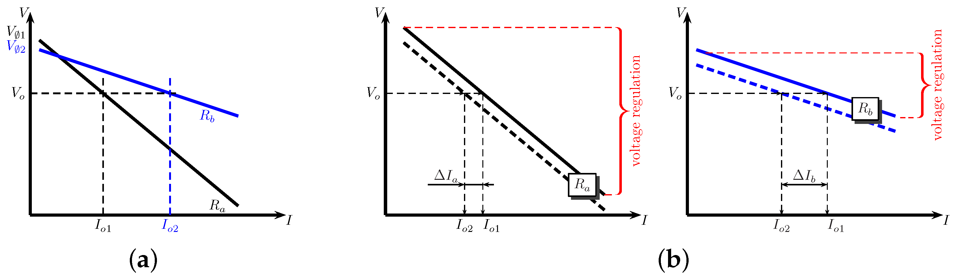
On the other hand, a passive method that is called the “droop” method is implemented by linearly reducing the DC output voltage as the output current increases, without the use of external information. It can be easily carried out by connecting a resistor to the module output. Even though it is so simple, the resistor adds losses into the system. Figure 1a shows the V–I output characteristics for two modules when resistors are connected to the outputs. It is represented assuming that the resistance, and , and the output voltage with no load, and , are different.
When modules are parallel connected, they have an equal output voltage (Vo), so each has a different output current ( and ). When both modules have the same added resistance, output characteristics can be obtained as shown in Figure 1b, in which it can be seen that current sharing depends on impedance. The smaller the difference between the elements, the better the current distribution and its effects can be minimized by increasing the slope, although the voltage regulation would become worse.
Another way to achieve this interdependency between voltage and current is through the existing control loop [11]. This behavior is a characteristic that can be found in some DC–DC topologies, such as resonant converters [12] that have high output impedances [13] or converters in discontinuous conduction mode (DCM) [14]. In these cases, the converter behaves as if it had a resistive element connected to its output, but without added losses.
Active clamp topologies [15] have high impedances [16,17], which makes them suitable for parallel connection and able to achieve passive current sharing within a modular system. In these topologies, zero voltage switching (ZVS) is possible under certain conditions, which reduces switching losses and improves converter efficiency. To extend the ZVS to lower power levels, an additional inductance is usually added.
After all of these considerations, the active clamp flyback (ACF) becomes a potential candidate for use as a module for an IPOP multiphase converter, through which the load sharing would be guaranteed without increasing the complexity of the control loop.
Nevertheless, the influence of the transformer must be taken into account, as it adds parasitic elements into the circuit and causes resonances with other elements. Moreover, when the transformation ratio is high, the resonances are magnified. The resonances can change the behavior of the converter [18] by modifying the expected current sharing.
Therefore, to improve current sharing in an ACF multiphase converter, the resonances must be minimized. Different approaches have been proposed: the RC–RCD snubber [19], which has the drawback of increasing losses; the inclusion of an additional diode to clamp the voltage and avoid resonances [20,21], although this has not been applied to a flyback; and the use of a voltage doubler for the integrated boost flyback topology [22]. In the last case, resonances are minimized and the transformation ratio is reduced. A similar solution has been used in an ACF topology as first stage of a solar micro-inverter design in [23].
In a previous paper [24], it was detected that the load sharing was not as good as existing models predicted. Resonances were identified as the cause, but were not modeled or analyzed in detail. In that paper, experimental results were obtained for the proposed solution that were based on the use of a diode to clamp the voltage, which showed a better current sharing between modules.
This paper deals with the reasons for bad current sharing in depth and demonstrates how minimal differences between parasitic capacitances have a great impact on power distribution. In this paper, we analyzed the following topics, which have not been studied before:
- Obtaining an analytical expression that relates the output voltage to the output current when there are no parasitic elements, i.e., the converter output characteristics, which show how modules can share the current and the effects of the tolerances;
- Obtaining the output characteristics, including the parasitic terms, and comparing them to data that were obtained using simulations (since they are based on parameters that are difficult to measure in practice);
- An in-depth analysis of the new topology using the clamp that was proposed in [24], which describes and studies the stages within a cycle;
- Obtaining an analytical expression of the output characteristics when the clamp diode is incorporated, including the parasitic elements, and its validation using simulations;
- Comparing the output characteristics when the clamp diode and parasitic elements are included to find the ideal configuration. Using this, it can be checked that they are quite close, even for large variations in the parasitic capacities.
The paper is organized as follows. In Section 2, the principles of the operation of an ACF and the effects of resonances in load sharing are explained. This section also includes how to obtain the analytical expression of the output characteristics, including the expression for when parasitic elements are incorporated. A modified topology to alleviate these effects is shown in Section 3. In Section 4, the experimental results are presented and our conclusions are reported in Section 5.
2. Analysis of Active Clamp Flyback Converter
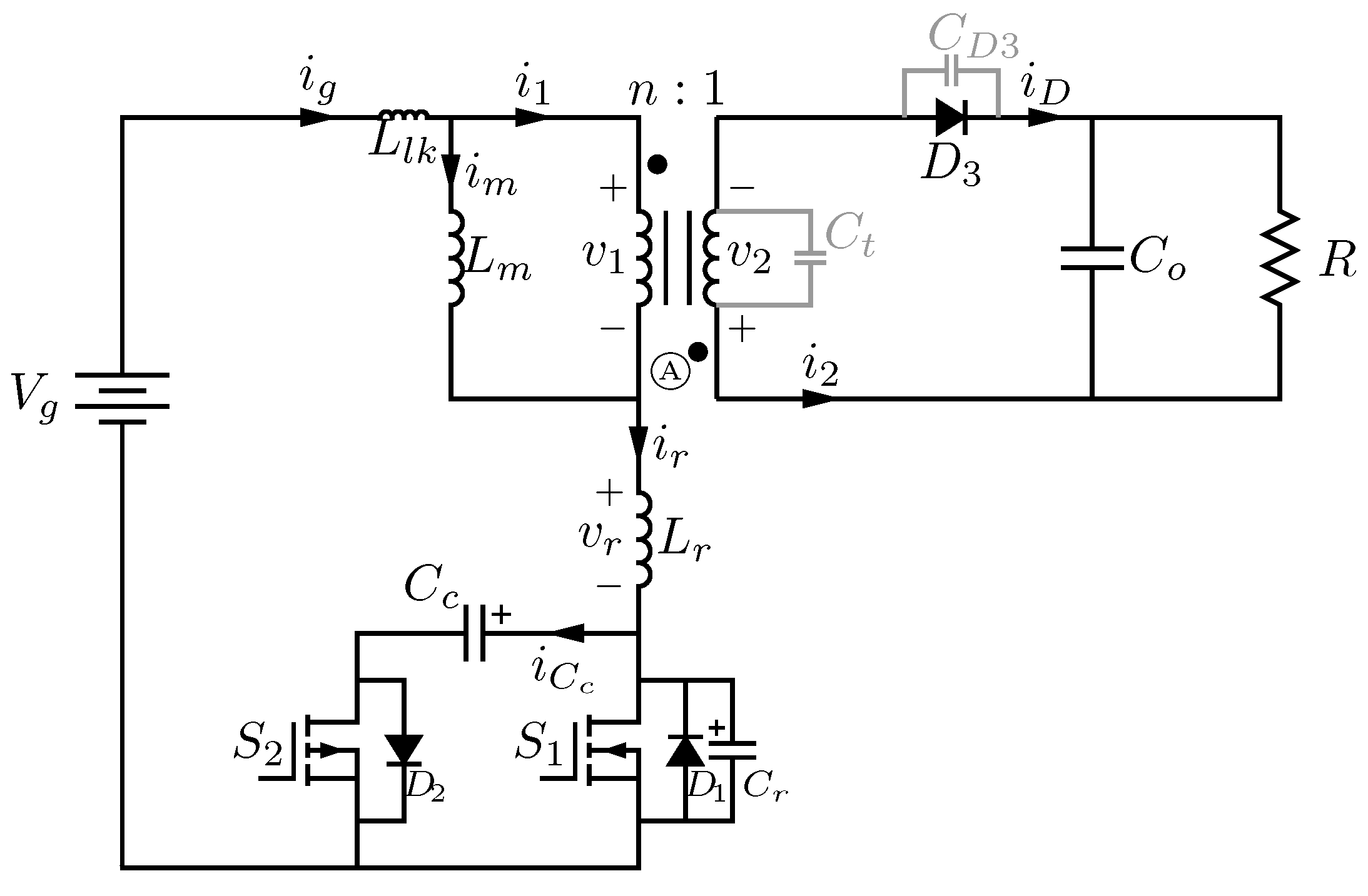
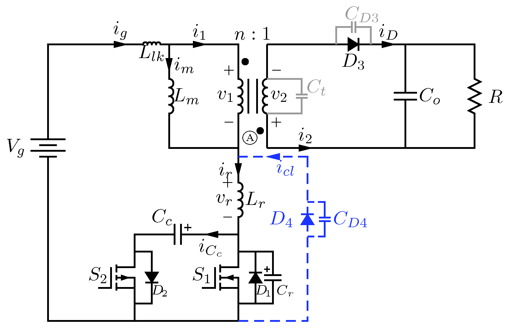
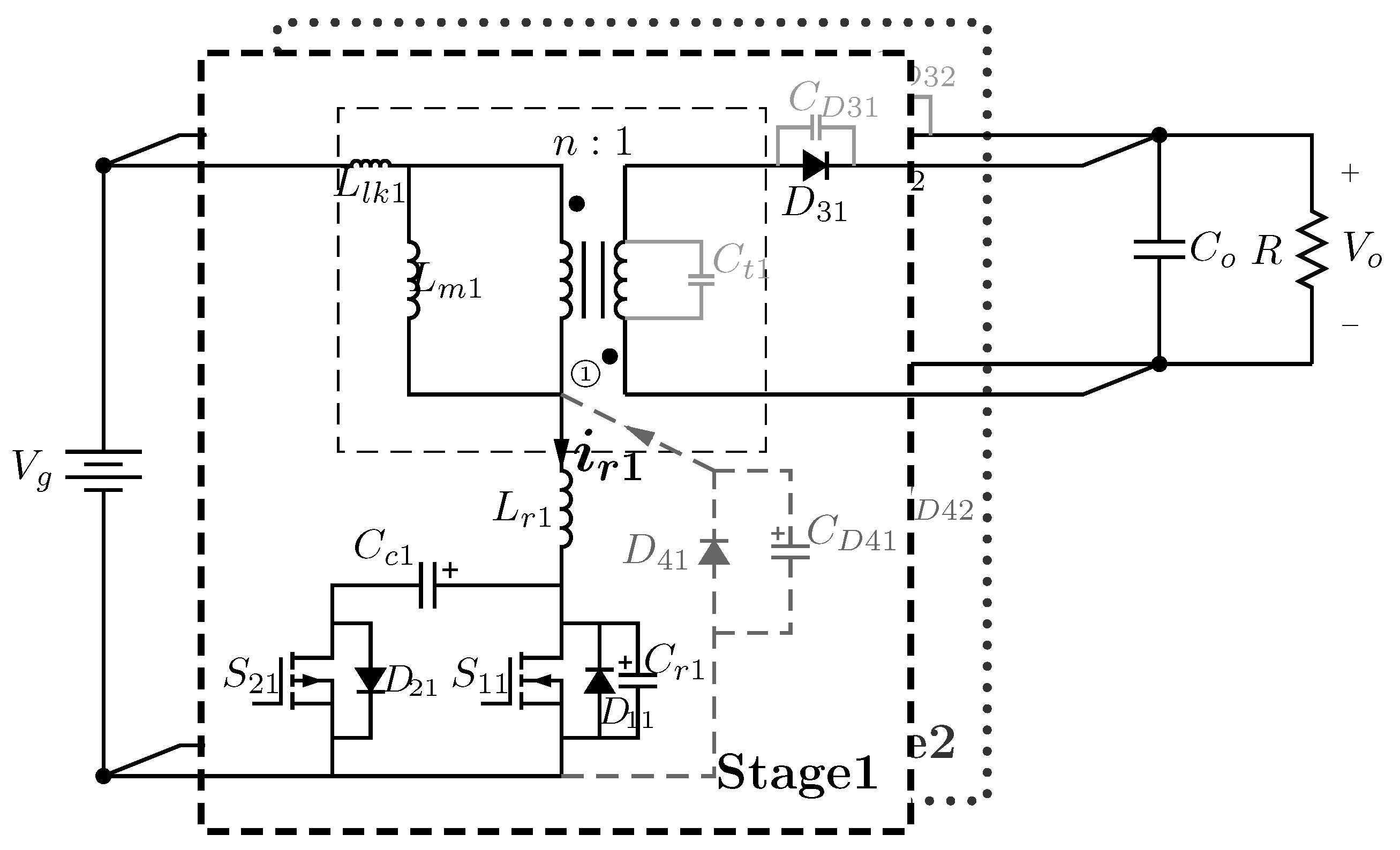
ACF converters have been previously analyzed in [25] and the topology that was selected in this paper is shown in Figure 2. It comprises a main switch (which includes its body diode ), a magnetizing inductance , with m being the transformer ratio and an output diode . The active clamp network includes an auxiliary switch (which includes its body diode ) and a clamp capacitor . An additional inductor could be included to extend the ZVS for a wider load range. The parasitic components are also shown in the same figure: the transformer parasitic components and and the junction capacitance of the output diode . A resonant capacitance represents the parallel combination of the parasitic capacitances of the two switches.
To understand how the parasitic components affect the current sharing between power stages in steady-state conditions, we explored how the currents are distributed among simplified ideal converters and what happens when they are taken into account.
2.1. Load Sharing under Ideal Behavior
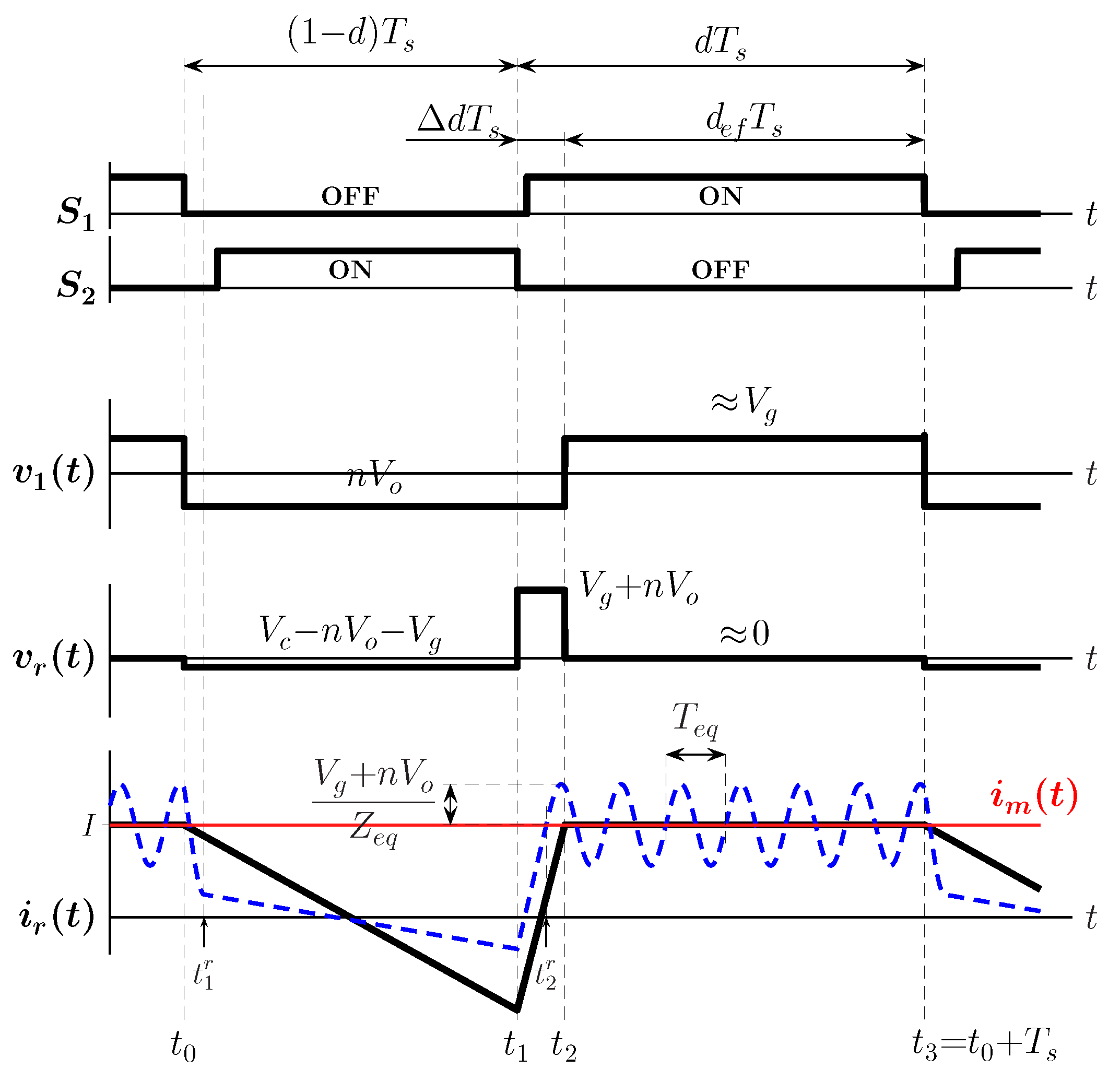
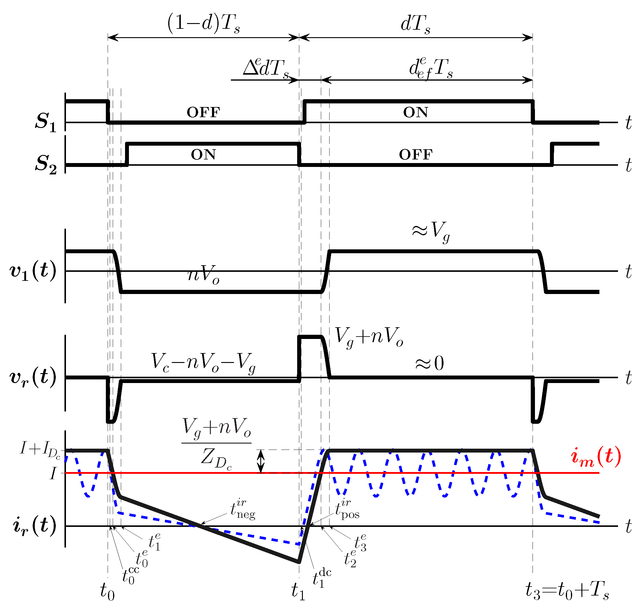
In Figure 3, the voltages to be applied to the magnetizing inductance and resonant inductor, and , respectively, are represented for an ideal converter. Curves for the resonant inductor when the converter is ideal (solid line) and when parasitic elements are considered (dashed line) are also included in the same figure.
The following simplifications were made. The magnetizing inductance was high enough to consider a ripple-free magnetizing current that was only compromised by its average value I, as can be seen in Figure. was much less than and the leakage inductance was assumed to be small enough to be included in . The output and clamp capacitors were also high enough to have constant voltages and , respectively. On the other hand, the main and auxiliary switches were treated as ideal components. They operated in a complementary way with a constant duty cycle d. The circuit behavior could be divided into six time intervals over the switching period . In the following description, three of them are neglected because they were short amounts of time and the resonant intervals were very fast at charging–discharging . These operations are only cited when they took place.
- Time interval : Prior to , was on and the same constant current was passing through and and . When the main switch was turned off at , the resonant current charged very quickly. After that, the current was directed to the clamp capacitor through the auxiliary diode and the auxiliary switch could be switched on at zero voltage. The output diode was forward-biased at this point and energy could be transferred to the output through the coupled inductors. The current was identified as the reversed secondary side current and was related to the primary current by a factor of n. On the other side, and exchanged energy in a resonant way. The resonant current became reversed and had a negative value at the end of this interval.
- Time interval : At , was switched off and the resonant current evolved from , a negative value, into a positive value under constant voltage for the majority of the time. Firstly, the resonant current helped to discharge very quickly. Secondly, the resonant current flowed across , thereby allowing a zero voltage switching of the main switch before became a zero value. Finally, when obtained a positive value, it flowed through until it matched to magnetizing current at . The output diode was reverse-biased at this moment.
- Time interval : From to the end of the switching period at , the same current was passing through and , which increased their stored energy.
By applying the volt-second balance in over the switching period, the output voltage was derived as (1), considering as the duty cycle variation. It was related to :
The output voltage of the ACF seemed to be similar to the output voltage of the conventional flyback in CCM when the term was collected in a single term , which named the effective duty cycle. It was related to the time interval during which was effectively charged.
The charge balance in led to . Then, an expression for was deduced from the current variations in at the time interval as (2). It revealed a direct dependence of duty cycle variation on the average value of the magnetizing current:
By combining Kirchhoff’s current law in node A with the current ratio in the coupled inductors, (3) was obtained:
By averaging (3) over one switching period and assuming ideal components, the output current and magnetizing current were related by (4). Then, depended on the output current in (5):
The last expression indicated that when the output current became higher, increased. Therefore, at a constant duty cycle value, the output voltage decreased when the output current increased. It looked as though a lossless resistance was placed at the converter output. Nevertheless, this dependence came from the existence of additional elements, which managed a portion of the processed energy even though it passed to the output. As more output power was required, more time to manage the stored energy was also needed.
The relationship between the duty cycle, output current and output voltage (6) could be deduced by combining (5) and (1):
The output impedance was obtained from the derivation of (6) with respect to . A more compact expression could be deduced when was isolated from (6) and introduced into the new expression, as shown in (7):
It revealed that the output impedance in steady-state conditions depended on and the input and output voltages, but there was no dependence on the duty cycle. Moreover, when N ideal ACF modules were parallel connected and used the same duty cycle, the output current for the k stage depended on every resonant inductor, as stated in (8):
2.2. Introducing the Effects of Parasitics
When parasitic capacitances were considered, exchanged energy with them in a resonant way after was switched off. The resonances modified the behavior of the converter and also affected the duty cycle variation . To bring together and on the primary side, an equivalent capacitance was defined as (9). A high turn ratio contributed toward enlarging its value:
The resonant current could be expressed as (10) during time interval , which is shown by the dashed line in Figure 3:
where
Two remarkable instants of time should be cited here. After was opened, the point in time where the resonant current equaled the changed from to and the point at which the voltage in reached using part of the current that was stored in was stated at . The output diode was forward-biased at the same time.
It must be stressed that the current at instant depended on the current at , which in turn depended on the current at . However, , as a consequence of the high value of , presented large variations, although only changed slightly.
By analyzing the current over the new intervals, the duty cycle variation under resonances was obtained using (12):
where , and are the time intervals and the clamp voltage in is .
By the charge balance at and , some relationships between the intervals were obtained:
The uncontrollable nature of resulted in nearly random changes in because it depended on the time intervals. They were interrelated with the circuit parameters, as is stated in the latter expressions.
It was very useful to show how the parasitic capacitances influence the output voltage–current relationship. A procedure to obtain the paired values of output voltage and output current was developed. An equation system comprising (12) and (13) mhad to be solved to obtain and values. Then, the output current value was calculated by combining (4) and (14).
2.3. Output Characteristic Curves
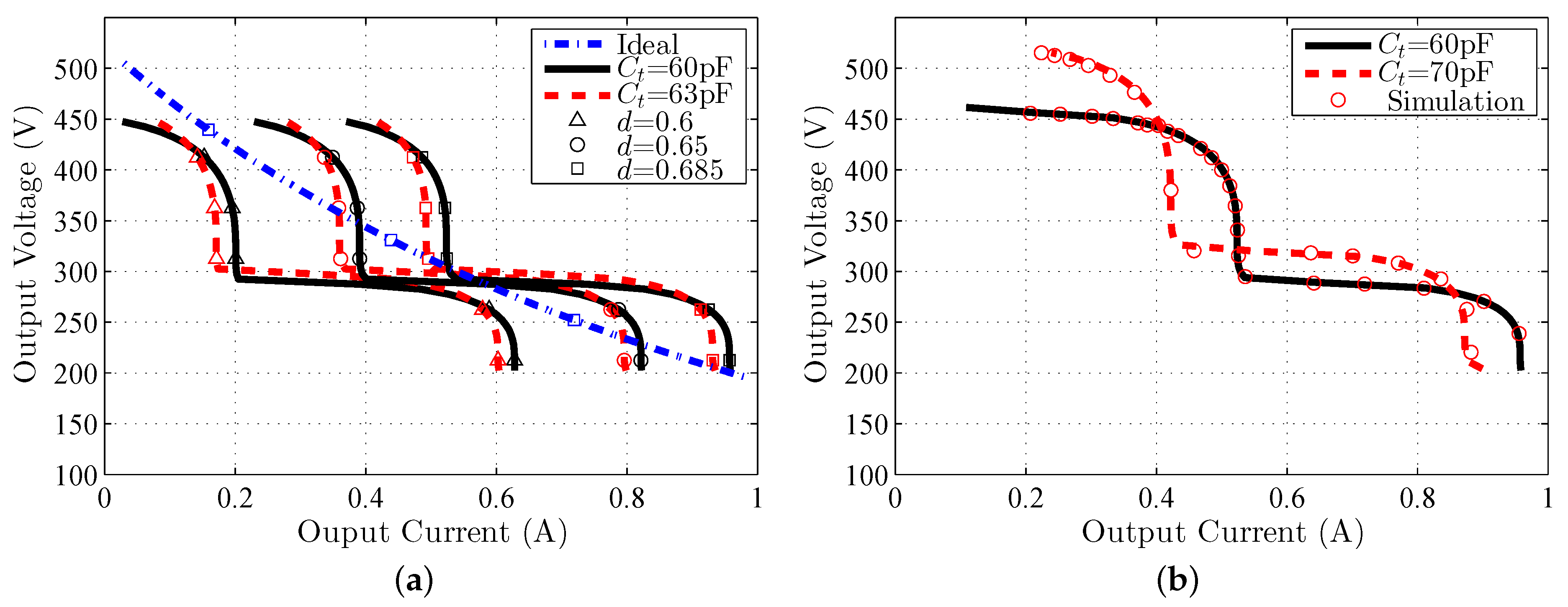
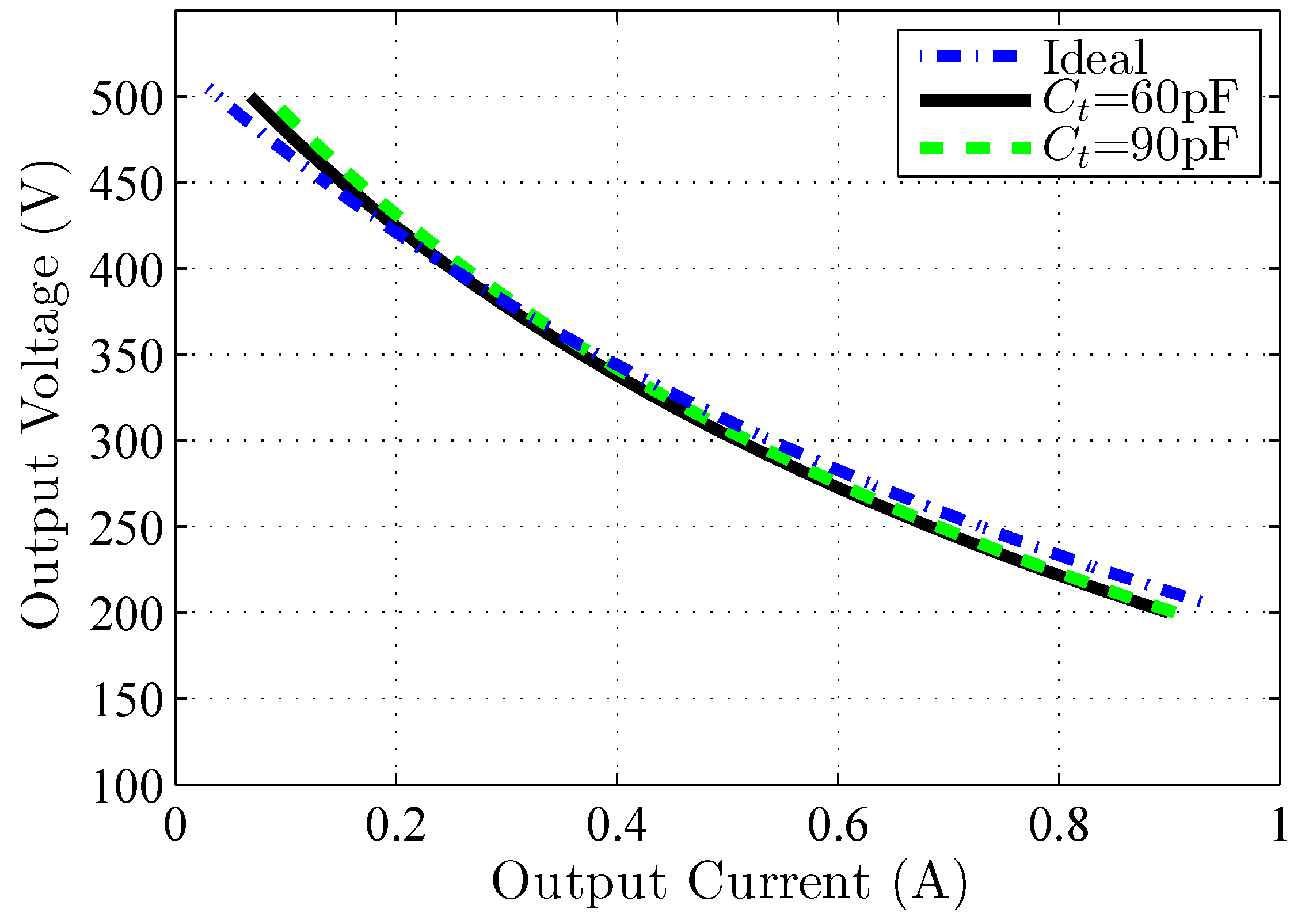
The output characteristics of the ideal case (6) is plotted in Figure 4a using the parameters that are included in Table 1. The ideal duty cycle was obtained by adding two terms: the effective duty cycle derived from (1) and the duty cycle variation in (5), considering an output current of A. In this way, , and .
Using the same parameters and duty cycles as the ideal case, the paired values were determined using the method that was described in the previous section when the parasitic capacitances were taken into account. The curves for 60 F and 63 F (a five percent variation) are shown in the same Figure while F. This method was repeated with duty cycle values of 0.6 and 0.65 and the curves were added to the same graph. The computer simulations of ACF with the parasitic elements showed a good agreement with the numerical calculations, as shown in Figure 4b.
As can be seen in all of the plotted curves, the output voltage generally decreased when the output current increased as an output impedance behavior. While a monotonous decreasing trend of the output impedance was observed in the represented ideal curve, when the parasitic capacitances were included, the output impedance evolved in a different way: it increased and decreased based upon the output voltage levels. For example, the slope of the curve was nearly flat at the output voltage around 300 V, regardless of the duty cycle value. A higher slope was also observed when the voltage was taken beyond or below this value for the same curves. The curves showed that a change in duty cycle did not alter the tendency for non-ideal curves but did produce a displacement.
Another interesting phenomena was the high sensitivity to parasitic capacitances in the same duty cycle. As depicted in Figure 4, a five percent variation in value was enough to cause a displacement in the output characteristics, while sustaining the output impedance trend. In this case, was chosen but the same effects were observed when was selected.
3. Enhanced ACF Topology
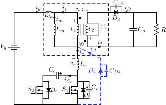
The proposed solution in this paper employed an unique diode to eliminate the resonances. This diode was considered to be ideal with no voltage drops. It was placed on the primary side between node A and the ground, as shown by the dashed line in Figure 5. The whole topology was an enhanced active clamp flyback (EACF). The added junction capacitance had a minor influence on the new circuit, but the voltage was fixed at a constant value after was turned on and the output impedance had a similar variation to the ideal case in Section 2.3. This solution was feasible because the resonant inductor was included in the ACF topology. When was not required, ringing between the parasitic capacitances and the leakage inductance could be mitigated, as exposed in [22].
3.1. Operating Principles
Prior to the present operation of the EACF, the parasitic capacitances and and the capacitance of the new diode were merged into and were fitted instead of , which had a value of (15):
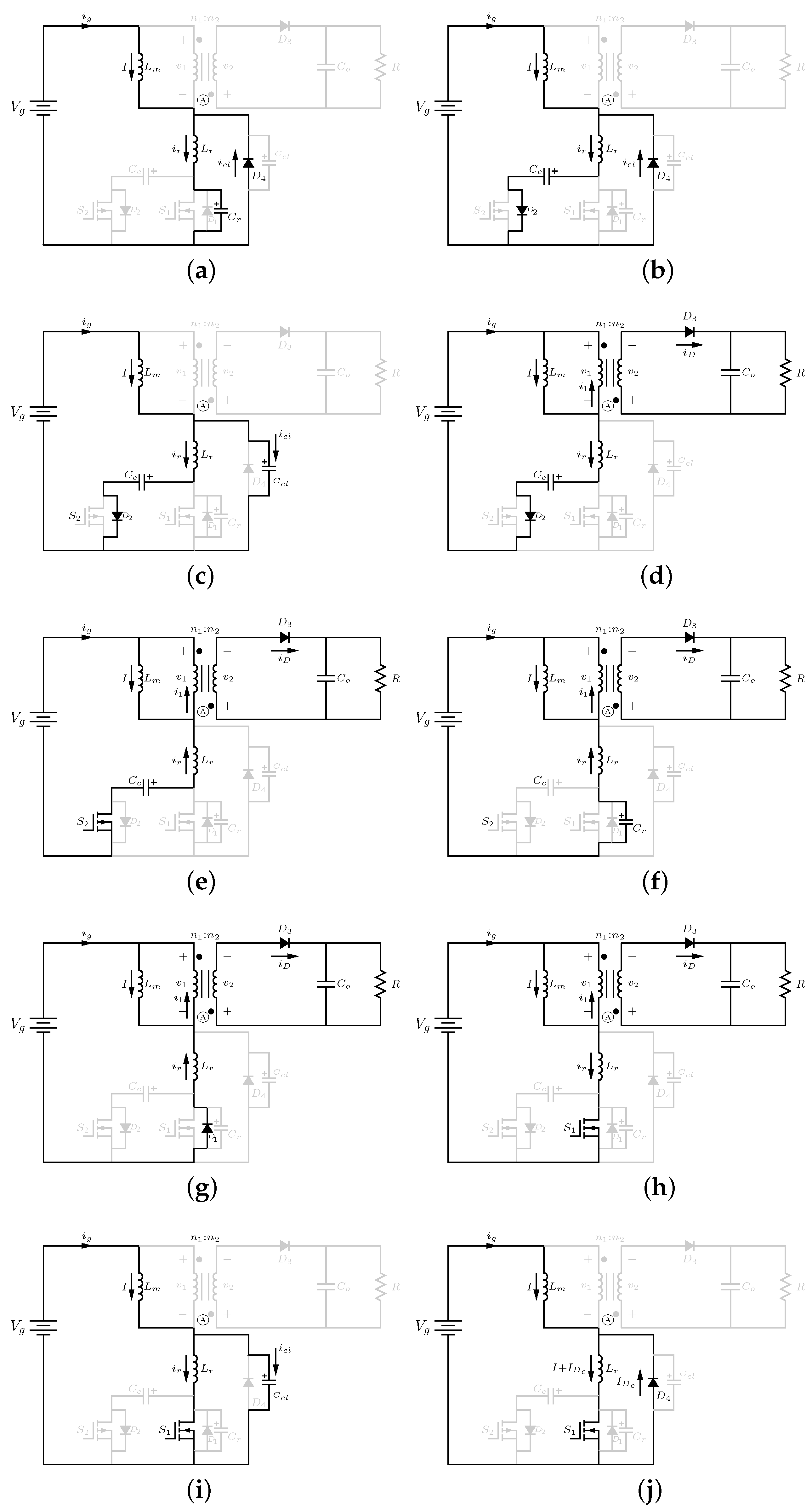
One switching period was divided into ten time intervals and the equivalent circuits of the EACF during each time interval are shown in Figure 6. The converter operated in continuous conduction mode (CCM) and the magnetizing inductance was high enough to consider a ripple-free current with a value of . The leakage inductance was included into the resonant inductor . The output and clamp capacitors were also high enough to have constant voltages and , respectively. The main and auxiliary switches were treated as ideal components. They operated in a complementary way with a constant duty cycle d.
The time intervals were detailed as follows:
- Time interval 1 ( Figure 6a): Prior to , the same current flowed through and . It comprised the magnetizing current I and the current from the diode branch . The main switch was turned off at and the resonant current rapidly charged until its voltage reached .
- Time interval 2 ( Figure 6b): After charging , the resonant current was redirected to through the auxiliary diode . exchanged energy with the clamp capacitor while the current decreased linearly to arrive at the value of I at . At this point, the current through became zero and was off.
- Time interval 3 ( Figure 6c): The resonant current decreased through capacitors and until the voltage in reached at . At this moment, was forward biased.
- Time interval 4 ( Figure 6d): Once started to conduct, energy was transferred to the output and the voltage that was applied to the resonant inductor became a negative value . Then, the resonant current was flowing through and decreased linearly until it reached zero value. To achieve the zero voltage switching of the auxiliary switch , it was necessary to turn on the transistor before the end of this interval, i.e., while its body diode was conducting.
- Time interval 5 ( Figure 6e): During this interval, circulated through the main body of until was switched off at . The resonant current decreased from zero to a negative value of .
- Time interval 6 ( Figure 6f): During this short time interval, the resonant current helped to discharge very quickly to zero voltage and barely changed its value.
- Time interval 7 ( Figure 6g): During this interval, the resonant current initially flowed across . It evolved from a negative value into a zero value under the constant voltage . To achieve the zero voltage switching of , it was required to turn on the transistor before the end of this interval.
- Time interval 8 ( Figure 6h): The resonant current evolved from a zero value into a positive value under the constant voltage and it circulated through the main body of until , at which point the resonant and magnetizing current equaled I. The output diode was reverse-biased.
- Time interval 9 ( Figure 6i): The energy that was stored in during interval 3 was returned to in a resonant form, which led to a current increment that was equal to at the final instant .
- Time interval 10 ( Figure 6j): From to the end of the switching period at , the same current was passing through and . The energy that was stored in and increased at the same time.
The expressions for the currents and voltages were obtained and the main theoretical curves are represented in Figure 7. It is worth noting that the point in time at which the resonant current equaled the magnetizing current changed from (or under ideal behavior) to . The point at which the voltage in reached was also stated at . The output diode was forward-biased during these two instants.
3.2. Steady-State Analysis
The relationship between the current and output voltage could be obtained from the steady-state analysis. Prior to that, it was necessary to calculate the duration the intervals. Time intervals 1 and 6 were neglected due to their short durations.
By using the volt-second balance in the magnetizing and resonant inductors, the clamp voltage in was derived as:
where , and are the time durations for the second, third and fourth intervals, respectively.
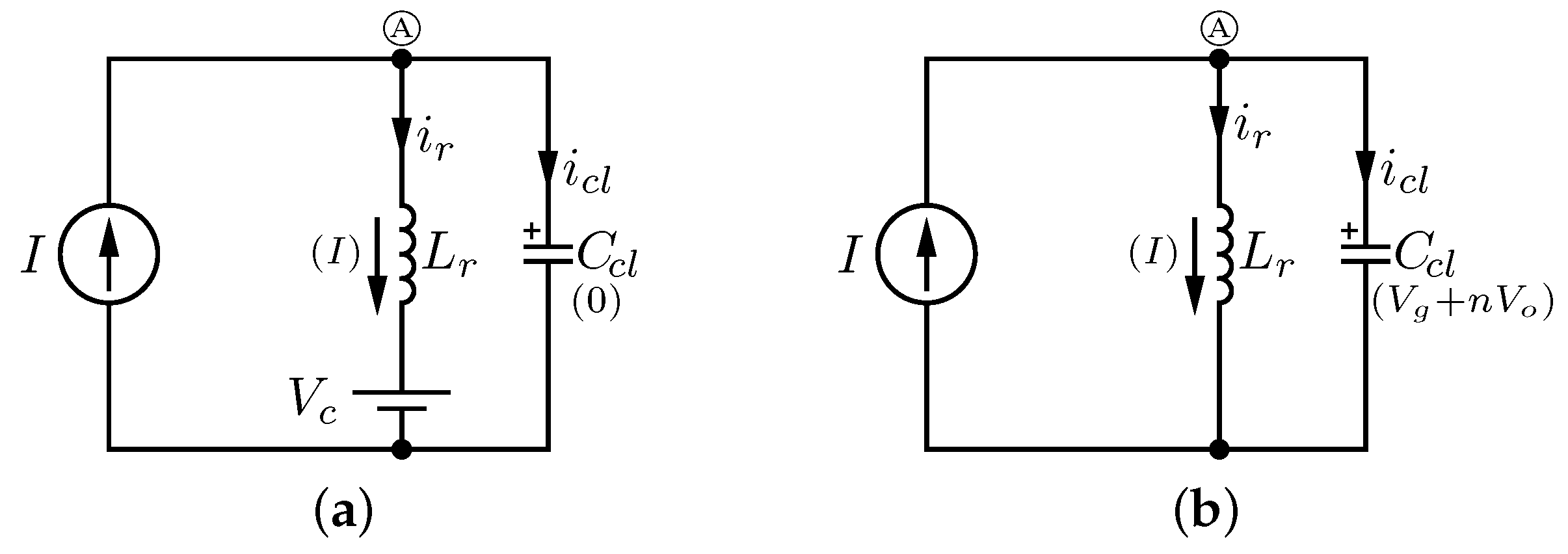
From the equivalent circuit for the third interval, as shown in Figure 8a, the charging time of could be derived using the knowledge that the voltage at the end of this stage was . Then, the voltage expression was indicated as (17):
where
Then:
Alternatively, for the equivalent circuit in Figure 8b, the discharging time of and its final current could be derived.
The voltage and current were expressed by expressions (20) and (21), respectively.
Assuming that was discharged at the end of this interval, the duration time denoted by became as in (22). The final current was deduced using (23) when a zero initial current was considered at the beginning:
During the second interval, variations in the resonant current under a constant voltage was accorded to . Then:
Knowing that and were both I, a relationship between , and was obtained:
3.3. Output Characteristic Curves
The relationship between the output voltage and output current (26) was obtained by combining the charge balances in and (4):
This curve is plotted in Figure 9 using the parameters that are included in Table 1 for a nominal output current of A. The duty cycle was the solution for (26) after replacing the clamp voltage and time intervals as a function of d. The resulting value was . Then, the output current values could be determined for every output voltage, while maintaining the duty cycle but recalculating the time intervals for the new output voltages.
In the same figure, the plot for a different value for is shown, which employed the same procedure but preserved the duty cycle. This comparison was interesting because identical duty cycles are used in parallel connected modules. Both curves were validated by the computer simulations. On the other hand, the output characteristics for the ideal ACF in Figure 4 were also included in order to compare the curves. It could be observed that:
- Regarding the real ACF curves, there was an important difference when the clamp diode was employed. Horizontal zones did not appear for the EAC when the parasitics were considered, which was an advantage when equal load sharing was required;
- The EACF curves were slightly affected by substantial changes in the parasitic capacitances. Then, load sharing was feasible independently of the parasitics because of its minor influence;
- The EACF curves had similar trends to those of the ideal ACF. Nevertheless, the duty cycle was different, although the operation parameters were identical. Moreover, for the enhanced topology, a smaller duty cycle was required to reach the same output voltage and current.
4. Experimental Results
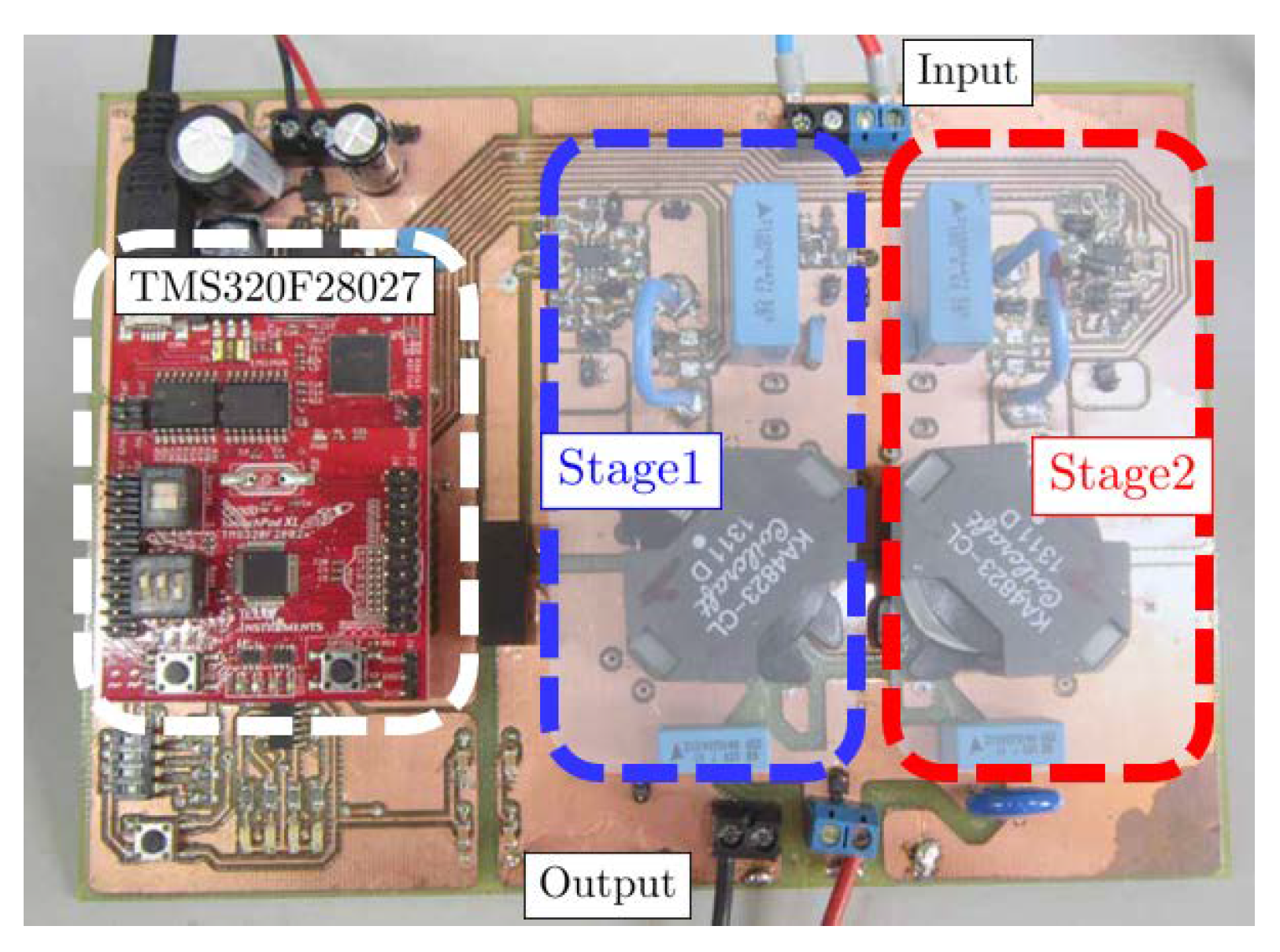
A laboratory prototype was built to verify the theoretical conclusions that were drawn in the previous sections. The prototype included two stages that were connected in parallel, as indicated in Figure 10, which shared the output capacitor. The prototype can be seen in Figure 11 and the main components are listed in Table 2. A TMS320F28027 microcontroller was employed to generate the PWM. Both stages were interleaved and shared the same duty cycle. Each stage was designed according to the specifications in Table 1. In order to check how the current sharing was affected by , different values were tested.
It was stated that theoretically EACF topologies have nearly the same output characteristics, i.e., for the same output voltage, they have nearly the same output current. In the other way, converters without clamp diodes cannot follow the same trend and the current sharing becomes worse in some regions of the I–V curve. To check this hypothesis, the voltage and current at the output were measured for both stages of the prototype when was included and when it was not. The measurements are graphically represented and compared in Figure 12a,b.
It must be noted that neither selection of passive components to minimize mismatches nor the identical printed circuit board design for each stage had been developed during the implementation stage of the prototype.
In all of the experiments, the output voltage decreased as the load increased, which implied that the converter exhibited an output impedance behavior. Nevertheless, the ACF stages presented substantial differences that could have led to a noticeable current imbalance. For example, the selection of for the output voltage of 205 V led to a current imbalance, without the clamp diode, of 71 mA over a total current of 686 mA. The current imbalance decreased to 12 mA over 637 mA when the clamp diode was introduced.
When a higher value for the resonant inductor was selected, the output impedance increased, as established in (7), and the current sharing was improved. This was only true for the EACF topology, but it was not be true for the ACF topology because the resonances altered the converter behavior and the output impedance increased or decreased depending on the region. Again, the measurements validated these findings, as shown in Figure 12b, where is 2 . A current difference of 9 mA was measured for the EACF but the difference for the ACF became worse, up to 103 mA. In this case, an output voltage of 185 V was chosen.
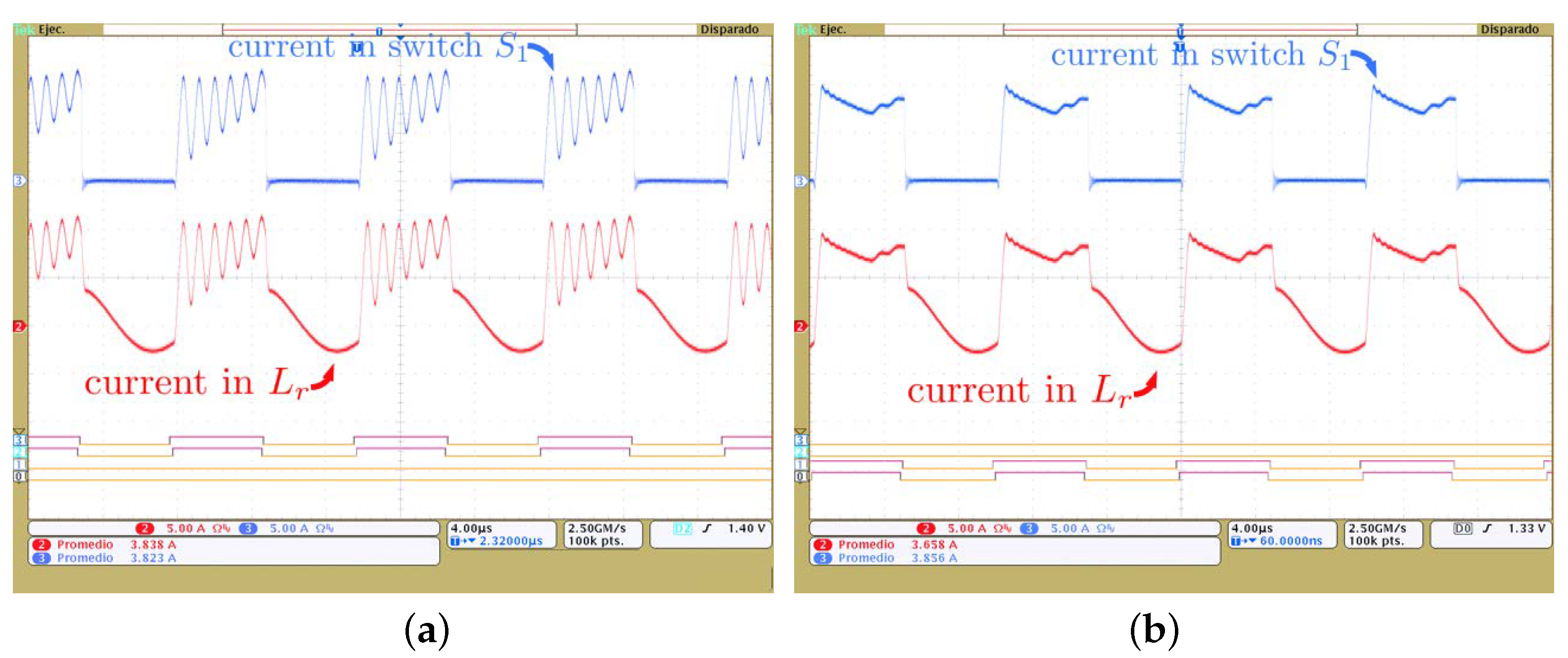
The resonances in and appeared when no clamp diode was used, as can be seen in Figure 13a. When it was introduced, both resonances were mitigated, as can be seen in Figure 13b.
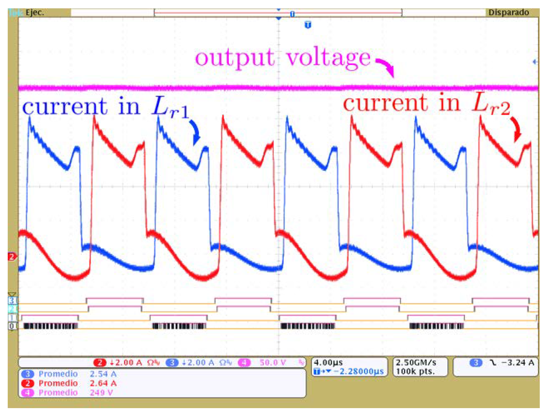
We noticed that when the main switch was closed (time interval 10), the currents did not evolve as expected. They resembled an inverted triangle. This difference was a consequence of the assumption of an ideal clamp diode in the theoretical analysis. In the laboratory, the forward voltage drop of the diode forced a slight decrease in the resonant current until equaled . After that, the current increased again until the end of the time interval. Nevertheless, although the current in the resonant inductors could be seen for the two stages that the EACF interleaved, the load sharing was not affected, as can be seen in Figure 14. It could be checked both for similar shapes and values, according to a good current sharing in steady-state conditions.
As the ZVS condition stage depended on the managed power, the number of active stages could be a function of the output power. Then, the stages could be switched on or off to ensure zero voltage switching (ZVS) in a higher power range.
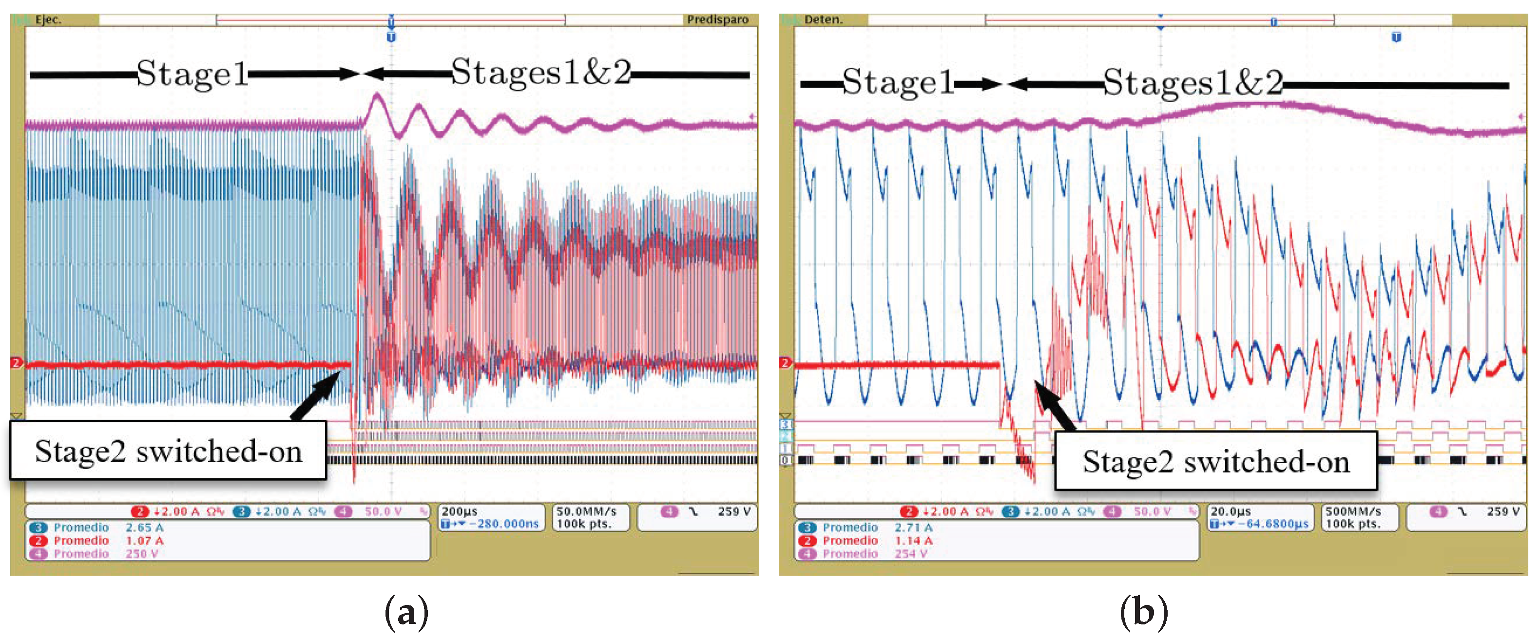
This mechanism was tested to check how the current sharing and converter behavior was affected. A good dynamic current balance was observed when stage2 was turned off, as shown in Figure 15, and when stage 2 was turned on, as shown in Figure 16. During both transients, the controller set up the converter in the new steady-state conditions without any additional mechanisms to preserve the individual currents in the stages. Finally, the efficiency was measured and was close to 94% for a wide load range.
5. Conclusions
In this paper, a solution to improve the static load sharing of active clamp flyback modules when connected in parallel was proposed. It was necessary to alleviate the ringing between the parasitic capacitances of the output diode and coupled inductors and the resonant inductor of the active clamp network because the converter behavior was altered and compromised the load sharing between the connected modules.
In order to develop a solution to that problem, the effects of parasitics in steady-state current balancing was studied in depth within a theoretical framework. A solution that was based on the placement of an additional diode was also analyzed theoretically. It was concluded that the proposed solution was valid and could help to minimize resonances and, therefore, help to obtain a better current balance than without the diode.
The theoretical conclusions were checked with a laboratory prototype. The experimental measurements that were carried out using the two-stage prototype showed a good agreement with the theoretical analysis. Moreover, a good current sharing was achieved in open loop without any dedicated methods being used to assure the current sharing once the resonances disappeared due to the added diode. Finally, this solution suggested that the IPOP connection of multiple active clamp flyback modules did not need any additional mechanisms for current balancing in the converter control loop.
Author Contributions
J.M.J.-M. performed the theoretical analysis, circuit implementation and experimental testing and wrote the original draft paper; E.d.J. helped in the investigation and contributed to the theoretical analysis; J.V. was responsible for funding acquisition, investigation, supervision, conceptualization, experimental testing and the reviewing and editing of the paper. All authors have read and agreed to the published version of the manuscript.
Funding
This research was funded by the Ministerio de Economia y Competitividad, grant number TEC2016-80136P.
Institutional Review Board Statement
Not applicable.
Informed Consent Statement
Not applicable.
Data Availability Statement
Not applicable.
Conflicts of Interest
The authors declare no conflict of interest.
References
- Knabben, G.C.; Zulauf, G.; Schäfer, J.; Kolar, J.W.; Kasper, M.J.; Azurza Anderson, J.; Deboy, G. Conceptualization and Analysis of a Next-Generation Ultra-Compact 1.5-kW PCB-IntegratedWide-Input-Voltage-Range 12V-Output Industrial DC/DC Converter Module. Electronics 2021, 10, 2158. [Google Scholar] [CrossRef]
- Kasper, M.; Bortis, D.; Kolar, J.W. Scaling and balancing of multi-cell converters. In Proceedings of the IEEE International Power Electronics Conference (IPEC-Hiroshima 2014—ECCE ASIA), Hiroshima, Japan, 18–21 May 2014; pp. 2079–2086. [Google Scholar] [CrossRef]
- Luo, S. A review of distributed power systems part I: DC distributed power system. IEEE Aerosp. Electron. Syst. Mag. 2005, 20, 5–16. [Google Scholar] [CrossRef]
- Roy, S.; Joisher, M.; Hanson, A.J. A Decentralized Nonlinear Control Scheme for Modular Power Sharing in DC-DC Converters. In Proceedings of the 2021 IEEE Energy Conversion Congress and Exposition (ECCE), Vancouver, BC, Canada, 10–14 October 2021; pp. 2798–2805. [Google Scholar] [CrossRef]
- Chen, W.; Ruan, X.; Yan, H.; Tse, C.K. DC/DC Conversion Systems Consisting of Multiple Converter Modules: Stability, Control, and Experimental Verifications. IEEE Trans. Power Electron. 2009, 24, 1463–1474. [Google Scholar] [CrossRef]
- Cheng, J.; Shi, J.; He, X. A novel input-parallel output-parallel connected DC-DC converter modules with automatic sharing of currents. In Proceedings of the 7th International Power Electronics and Motion Control Conference, Harbin, China, 2–5 June 2012; Volume 3, pp. 1871–1876. [Google Scholar] [CrossRef]
- Shi, J.; Zhou, L.; He, X. Common-Duty-Ratio Control of Input-Parallel Output-Parallel (IPOP) Connected DC-DC Converter ModulesWith Automatic Sharing of Currents. IEEE Trans. Power Electron. 2012, 27, 3277–3291. [Google Scholar] [CrossRef]
- Luo, S.; Ye, Z.; Lin, R.L.; Lee, F. A classification and evaluation of paralleling methods for power supply modules. In Proceedings of the 30th Annual IEEE Power Electronics Specialists Conference (PESC 99), Charleston, SC, USA, 1 July 1999; Volume 2, pp. 901–908. [Google Scholar] [CrossRef]
- Balogh, L. Paralleling Power-Choosing and Applying the Best Technique for Load Sharing. In Texas Instruments/UNITRODE Power Design Seminar SLUP207; Texas Instruments: Dallas, TX, USA, 2002; pp. 6-1–6-30. [Google Scholar]
- Vazquez, A.; Rodriguez, A.; Lamar, D.G.; Hernando, M.M. Advanced Control Techniques to Improve the Efficiency of IPOP Modular QSW-ZVS Converters. IEEE Trans. Power Electron. 2018, 33, 73–86. [Google Scholar] [CrossRef] [Green Version]
- Anand, S.; Fernandes, B. Modified droop controller for paralleling of DC-DC converters in standalone dc system. IET Power Electron. 2012, 5, 782–789. [Google Scholar] [CrossRef]
- Ahmad, U.; Cha, H.; Naseem, N. Integrated Current Balancing Transformer Based Input-Parallel Output-Parallel LLC Resonant Converter Modules. IEEE Trans. Power Electron. 2021, 36, 5278–5289. [Google Scholar] [CrossRef]
- Alemdar, O.S.; Keysan, O. Design and implementation of an unregulated DC-DC transformer (DCX) module using LLC resonant converter. In Proceedings of the 8th IET International Conference on Power Electronics, Machines and Drives (PEMD 2016), Glasgow, UK, 19–21 April 2016; pp. 1–6. [Google Scholar] [CrossRef]
- de Jesus Kremes, W.; Ewerling, M.V.M.; Illa Font, C.H.; Lazzarin, T.B. Analysis of Self-sharing of Currents in Steady-state of IPOP Connected Modular SEPIC Converter in DCM. In Proceedings of the 2018 9th IEEE International Symposium on Power Electronics for Distributed Generation Systems (PEDG), Charlotte, NC, USA, 25–28 June 2018; pp. 1–7. [Google Scholar] [CrossRef]
- Duarte, C.; Barbi, I. A family of ZVS-PWM active-clamping DC-to-DC converters: Synthesis, analysis, design, and experimentation. IEEE Trans. Circuits Syst. I Fundam. Theory Appl. 1997, 44, 698–704. [Google Scholar] [CrossRef]
- De Jodar, E.; Villarejo, J.; Suardiaz, J.; Soto, F. Effect of the Output Impedance of Active Clamp Topology in Multiphase Converters. In Proceedings of the 2007 IEEE International Symposium on Industrial Electronics, Vigo, Spain, 4–7 June 2007; pp. 566–571. [Google Scholar] [CrossRef] [Green Version]
- Villarejo, J.; de Jodar, E.; Soto, F.; Moreno, M. Multistage Active-Clamp High Power Factor Rectifier with passive lossless current sharing. In Proceedings of the Energy Conversion Congress and Exposition, ECCE 2009, San Jose, CA, USA, 20–24 September 2009; pp. 948–953. [Google Scholar] [CrossRef]
- Spiazzi, G.; Mattavelli, P.; Costabeber, A. Effect of parasitic components in the integrated boost-flyback high step-up converter. In Proceedings of the 35th Annual Conference of IEEE Industrial Electronics (IECON ’09), Porto, Portugal, 3–5 November 2009; pp. 420–425. [Google Scholar] [CrossRef]
- Hren, A.; Korelic, J.; Milanovic, M. RC-RCD clamp circuit for ringing losses reduction in a flyback converter. IEEE Trans. Circuits Syst. Express Briefs 2006, 53, 369–373. [Google Scholar] [CrossRef]
- Duarte, C.; Barbi, I. An improved family of ZVS-PWM active-clamping DC-to-DC converters. IEEE Trans. Power Electron. 2002, 17, 1–7. [Google Scholar] [CrossRef]
- Masihuzzaman, M.; Lakshminarasamma, N. An improved ZVS-PWM, active clamp/reset forward converter: Analysis, design and dynamic model. In Proceedings of the IEEE 12th Workshop on Control and Modeling for Power Electronics (COMPEL), Boulder, CO, USA, 28–30 June 2010; pp. 1–8. [Google Scholar] [CrossRef]
- Spiazzi, G.; Mattavelli, P.; Costabeber, A. High Step-Up Ratio Flyback ConverterWith Active Clamp and Voltage Multiplier. IEEE Trans. Power Electron. 2011, 26, 3205–3214. [Google Scholar] [CrossRef]
- Bhardwaj, M.; Choudury, S. Digitally Controlled Solar Micro Inverter Design using C2000 Piccolo Microcontroller. In Texas Instruments User Guide TIDU405B; Texas Instruments: Dallas, TX, USA, 2017; pp. 1–54. [Google Scholar]
- Jimenez, J.M.; de Jodar, E.; Mateo, A.; Villarejo, J. Improving passive current sharing in multiphase active-clamp flyback converter with high step-up ratio. In Proceedings of the 19th European Conference on Power Electronics and Applications (EPE’17 ECCE Europe), Warsaw, Poland, 11–14 September 2017; pp. 1–7. [Google Scholar] [CrossRef]
- Watson, R.; Lee, F.; Hua, G. Utilization of an active-clamp circuit to achieve soft switching in flyback converters. IEEE Trans. Power Electron. 1996, 11, 162–169. [Google Scholar] [CrossRef]
Figure 1.
Output characteristics for two parallel connected modules with an added resistor at the output: (a) different values; (b) same values ( on the left and on the right when ).
Figure 1.
Output characteristics for two parallel connected modules with an added resistor at the output: (a) different values; (b) same values ( on the left and on the right when ).

Figure 2.
ACF converter with parasitic elements.

Figure 3.
Main curves for circuit in Figure 2: is plotted for the ideal case (solid) and when parasitic elements are included (dashed).
Figure 3.
Main curves for circuit in Figure 2: is plotted for the ideal case (solid) and when parasitic elements are included (dashed).

Figure 4.
Output voltage to output current curves for the circuit in Figure 2: (a) ideal case (dash-dot line) and considering two values for parasitic capacitances (solid and dashed lines) when different duty cycles (triangle, circle and square markers) were used; (b) comparison between the numerical results and the data obtained from computer simulations for the two parasitic capacitances.

Figure 5.
Enhaced ACF converter with parasitic elements and the proposed clamp (dashed line).

Figure 6.
Equivalent circuits of the EACF during a switching period: (a) time interval 1; (b) time interval 2; (c) time interval 3; (d) time interval 4; (e) time interval 5; (f) time interval 6; (g) time interval 7; (h) time interval 8; (i) time interval 9; (j) time interval 10. The capacitance represents all of the parasitic capacitances.

Figure 7.
Main theoretical waveforms of the EACF topology. The resonant current is plotted for the enhanced topology by the solid line and for the ACF with parasitics by the dashed line.
Figure 7.
Main theoretical waveforms of the EACF topology. The resonant current is plotted for the enhanced topology by the solid line and for the ACF with parasitics by the dashed line.

Figure 8.
Equivalent circuits: (a) during time interval 3; (b) during time interval 9. The initial conditions are in parentheses.
Figure 8.
Equivalent circuits: (a) during time interval 3; (b) during time interval 9. The initial conditions are in parentheses.

Figure 9.
Output voltage to output current curve for EACF using the selected values for parasitic capacitance () and ACF ().
Figure 9.
Output voltage to output current curve for EACF using the selected values for parasitic capacitance () and ACF ().

Figure 10.
Connection diagram of the prototype that was formed of two stages in parallel.

Figure 11.
Prototype with two parallell connected (IPOP) ACFs and a microcontroller.

Figure 12.
Experimental output voltage to output current curves for stages 1 and 2 in the ACF topology (dotted line) and EACF topology (solid line) for different values of the resonant inductor: (a) ; (b) .
Figure 12.
Experimental output voltage to output current curves for stages 1 and 2 in the ACF topology (dotted line) and EACF topology (solid line) for different values of the resonant inductor: (a) ; (b) .

Figure 13.
Current in and current in main switch : (a) Ccurves for the real ACF; (b) curves for the EACF. The value for the resonant inductor was in both experiments.
Figure 13.
Current in and current in main switch : (a) Ccurves for the real ACF; (b) curves for the EACF. The value for the resonant inductor was in both experiments.

Figure 14.
Measurement of the resonant inductor currents in both interleaving parallel connected EACF converters.
Figure 14.
Measurement of the resonant inductor currents in both interleaving parallel connected EACF converters.

Figure 15.
Closed loop dynamic response of resonant currents and output voltage: (a) when one stage was switched off; (b) expanded curves.
Figure 15.
Closed loop dynamic response of resonant currents and output voltage: (a) when one stage was switched off; (b) expanded curves.

Figure 16.
Closed loop dynamic response of resonant currents and output voltage: (a) when one stage was switched on; (b) expanded curves.
Figure 16.
Closed loop dynamic response of resonant currents and output voltage: (a) when one stage was switched on; (b) expanded curves.


Table 1.
Active clamp flyback parameters that were used to obtain the curves in Figure 4.
Table 1.
Active clamp flyback parameters that were used to obtain the curves in Figure 4.
| Parameters for the Output Voltage to Output Current Curves | ||
|---|---|---|
| V | : = 1:12 | |
| V | ||
| kHz | ||
| ns | 60 pF, 63 pF and 70 pF | |
Table 2.
Main components that were used in the prototype.
| Components | Value-Reference | Description |
|---|---|---|
| MOSFET | IRFS4321 | N-channel 150 V; mΩ @ = 10 V |
| MOSFET | IRF6218S | P-channel V; 150 mΩ @ = V |
| MOSFET Driver | MCP14E4 | 4.0 A Dual H-Speed MOSFET Driver |
| Diode | C4D05120E | SiC Schottky; 1200 V, 9A |
| Diode clamp | MUR420 | Ultrafast; 200 V , 4 A |
| Coupled Inductors | Coilcraft KA-4823CL | 1:12; 28 ; 8 mΩ DCR@ = |
| Resonant Inductor | Coilcraft SER2010-102L | 1; mΩ DCR |
| Coilcraft SER2010-202L | 2; mΩ DCR | |
| Clamp Capacitor | F | 250 V |
| Output Capacitor | F | 630 V |
| Input Capacitor | 10F + | 63 V |
Publisher’s Note: MDPI stays neutral with regard to jurisdictional claims in published maps and institutional affiliations. |
© 2022 by the authors. Licensee MDPI, Basel, Switzerland. This article is an open access article distributed under the terms and conditions of the Creative Commons Attribution (CC BY) license (https://creativecommons.org/licenses/by/4.0/).
Share and Cite
MDPI and ACS Style
Jiménez-Martínez, J.M.; de Jódar, E.; Villarejo, J. Parasitic Capacitance Effects on Active Clamp Flyback Output Characteristics: Application to IPOP Connection. Energies 2022, 15, 3201. https://0-doi-org.brum.beds.ac.uk/10.3390/en15093201
AMA Style
Jiménez-Martínez JM, de Jódar E, Villarejo J. Parasitic Capacitance Effects on Active Clamp Flyback Output Characteristics: Application to IPOP Connection. Energies. 2022; 15(9):3201. https://0-doi-org.brum.beds.ac.uk/10.3390/en15093201
Chicago/Turabian StyleJiménez-Martínez, Jacinto M., Esther de Jódar, and José Villarejo. 2022. "Parasitic Capacitance Effects on Active Clamp Flyback Output Characteristics: Application to IPOP Connection" Energies 15, no. 9: 3201. https://0-doi-org.brum.beds.ac.uk/10.3390/en15093201
Note that from the first issue of 2016, this journal uses article numbers instead of page numbers. See further details here.