
Multi-Port Multi-Directional Converter with Multi-Mode Operation and Leakage Energy Recycling for Green Energy Processing


Abstract
:1. Introduction
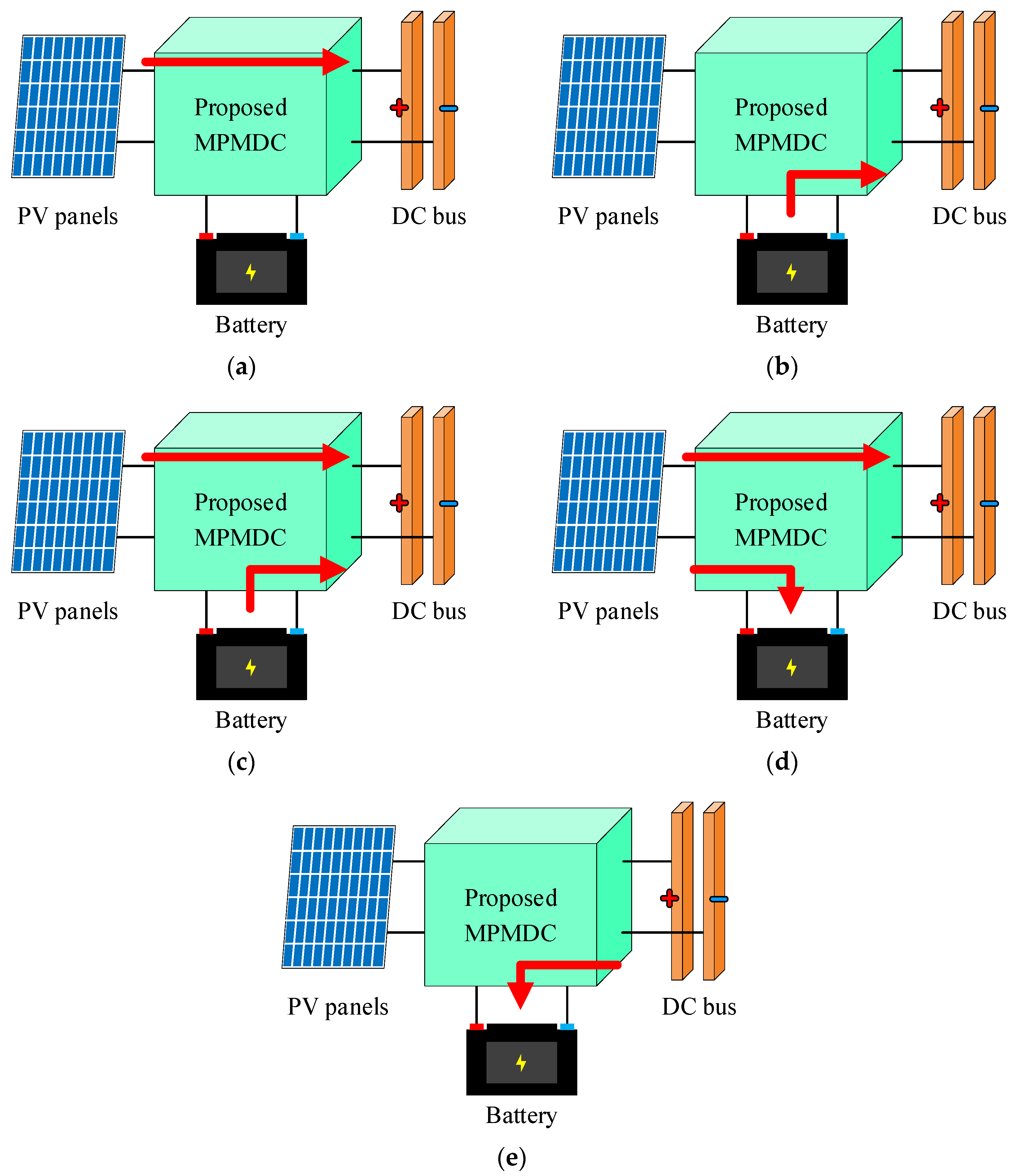
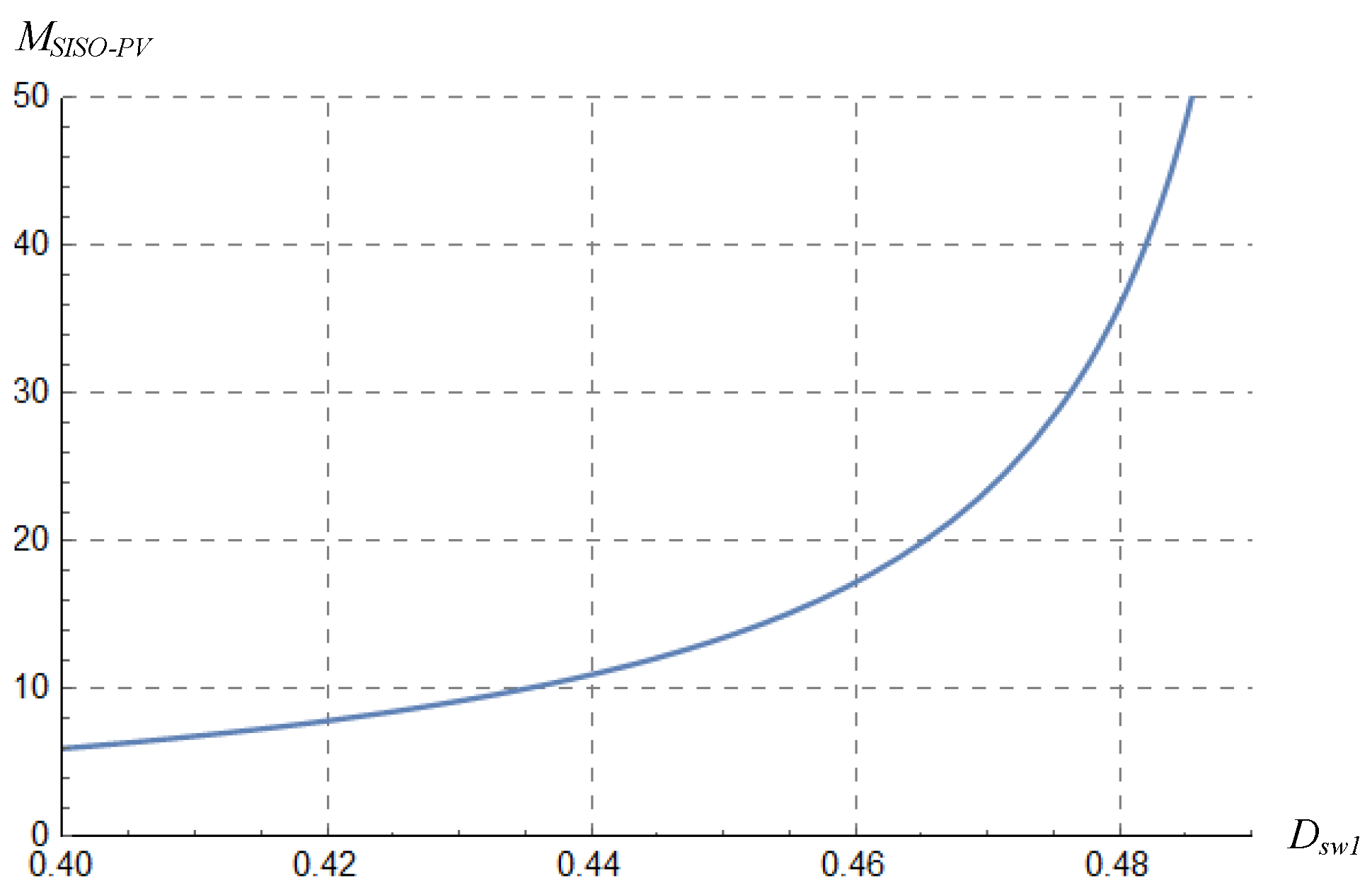
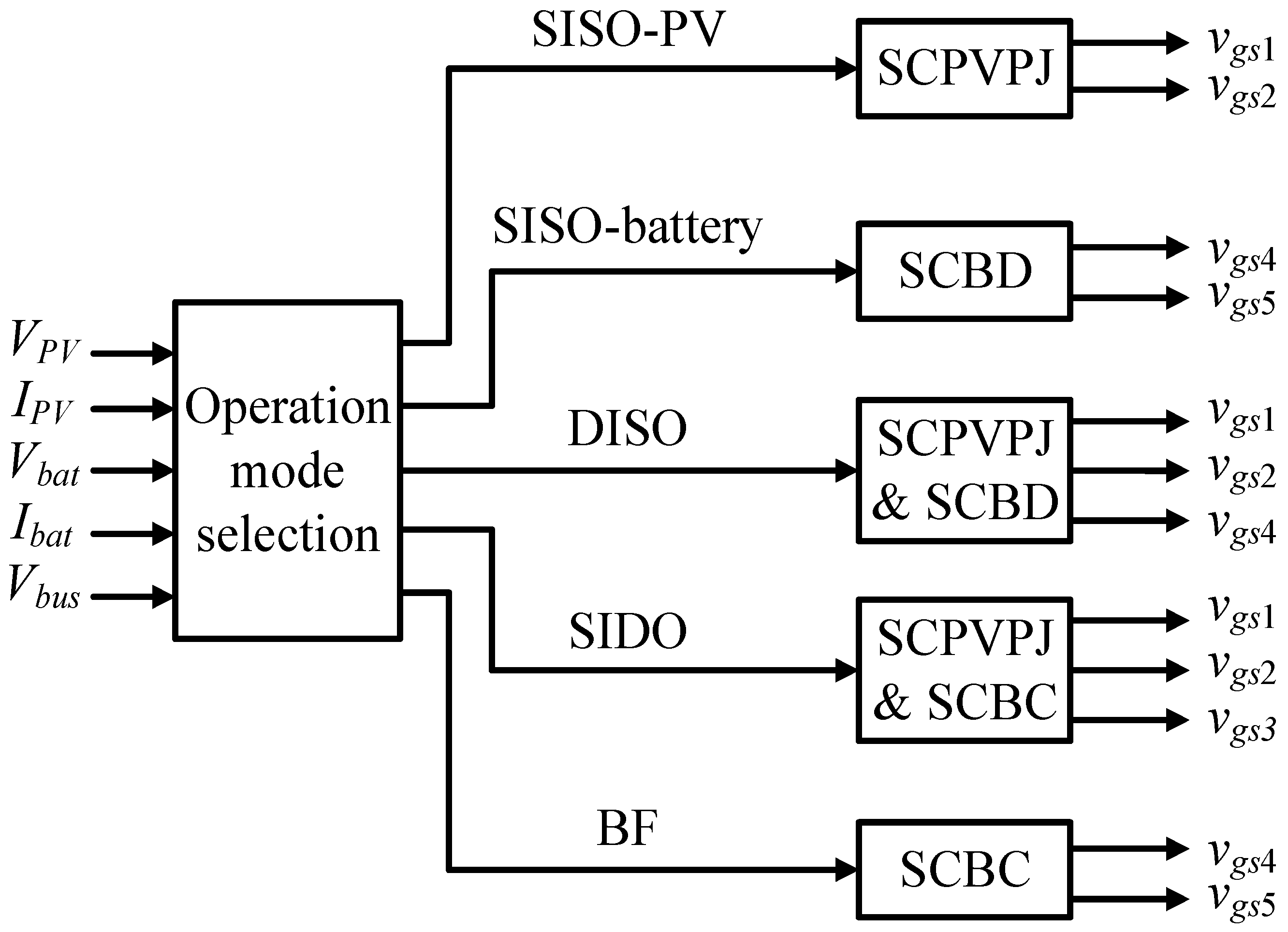
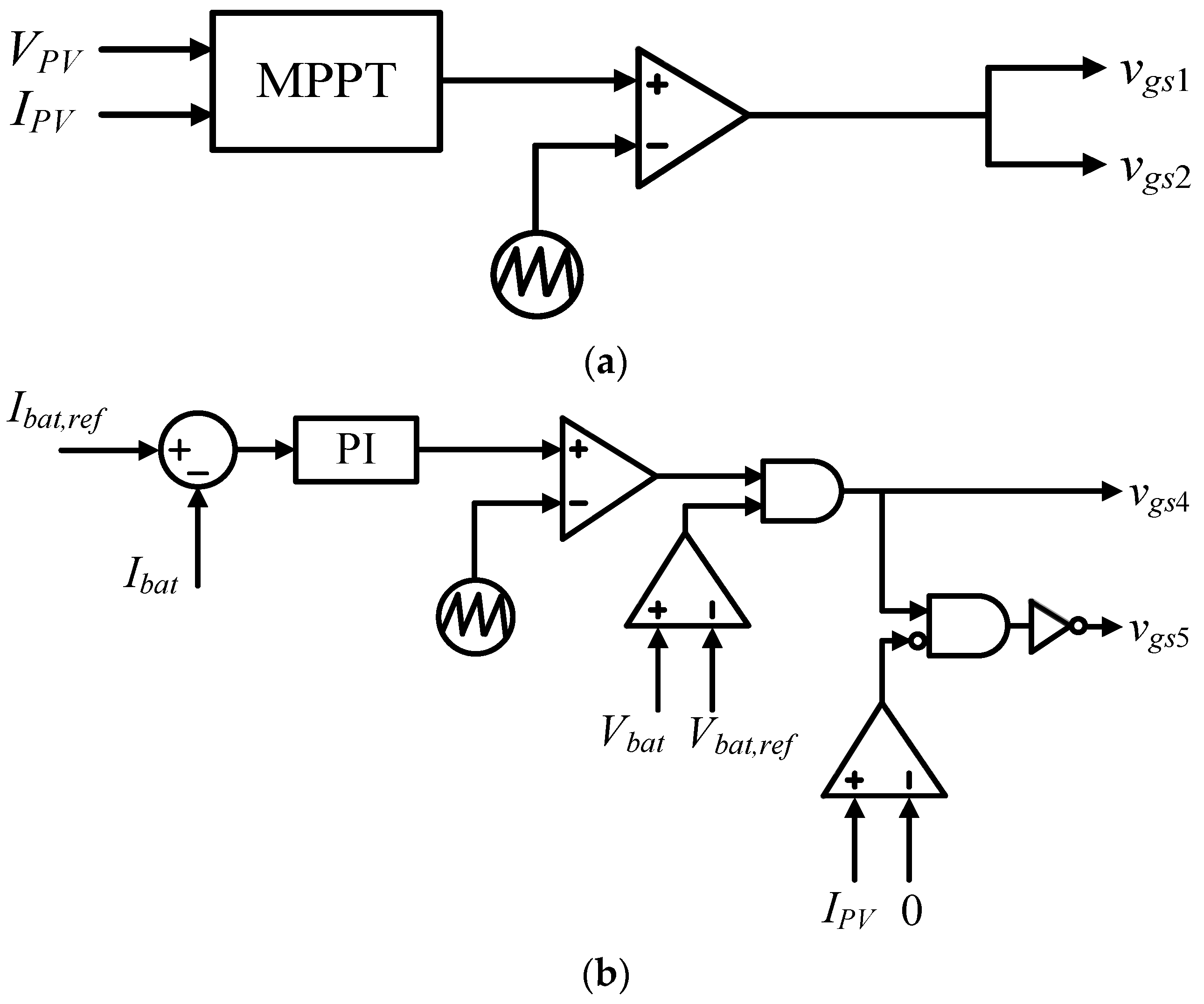
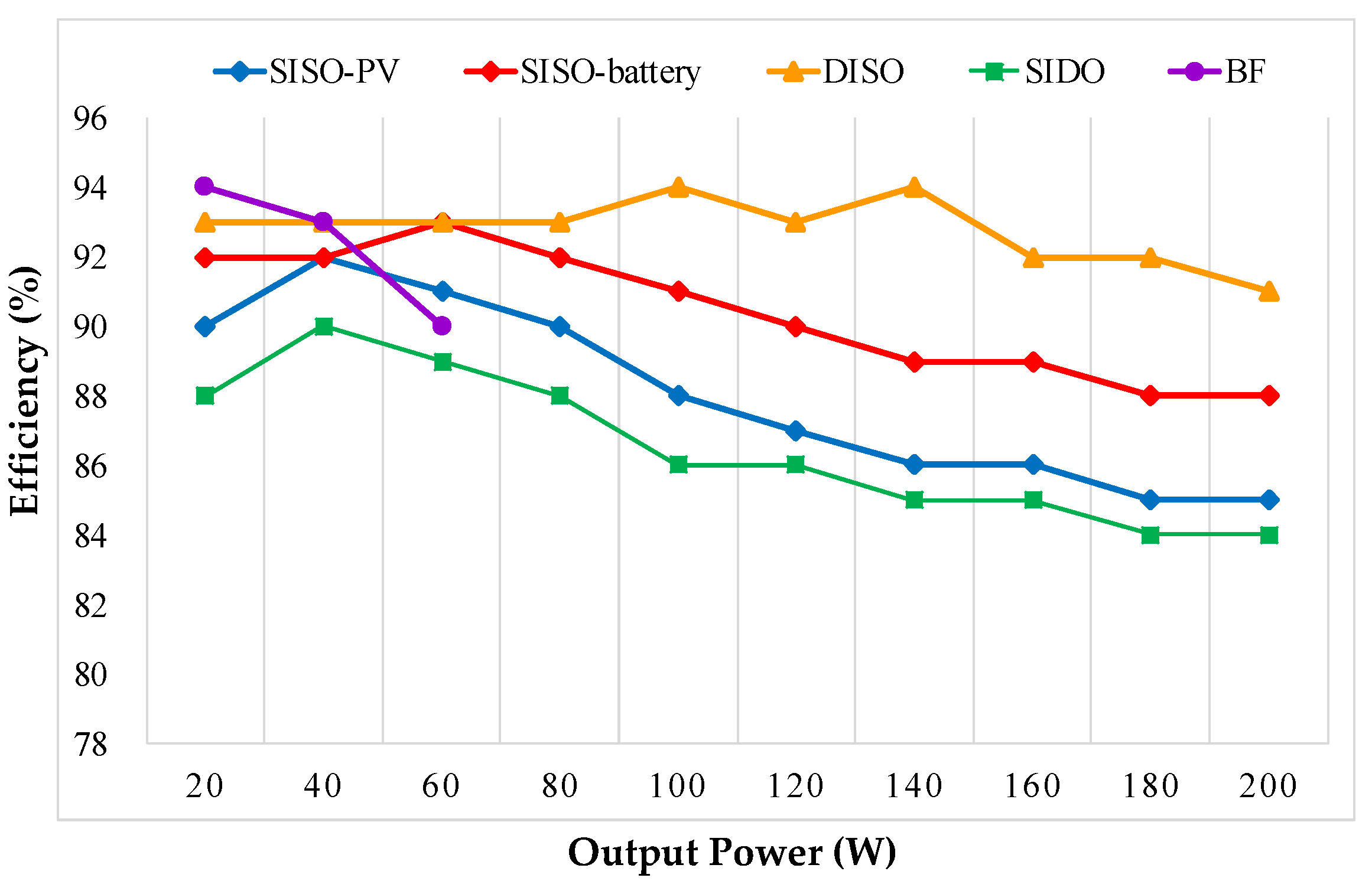
- Single input and single output for PV power processing (SISO-PV mode): Only the PV panels forward power to the DC bus, as shown in Figure 2a. In this mode, the battery has been fully charged and PV panels inject all the generated solar power into the DC bus;
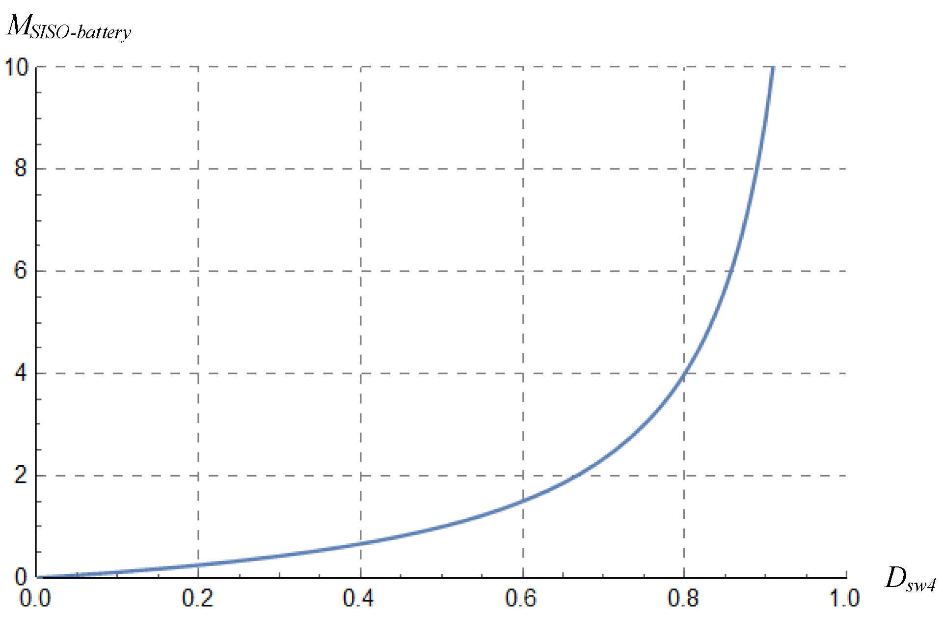
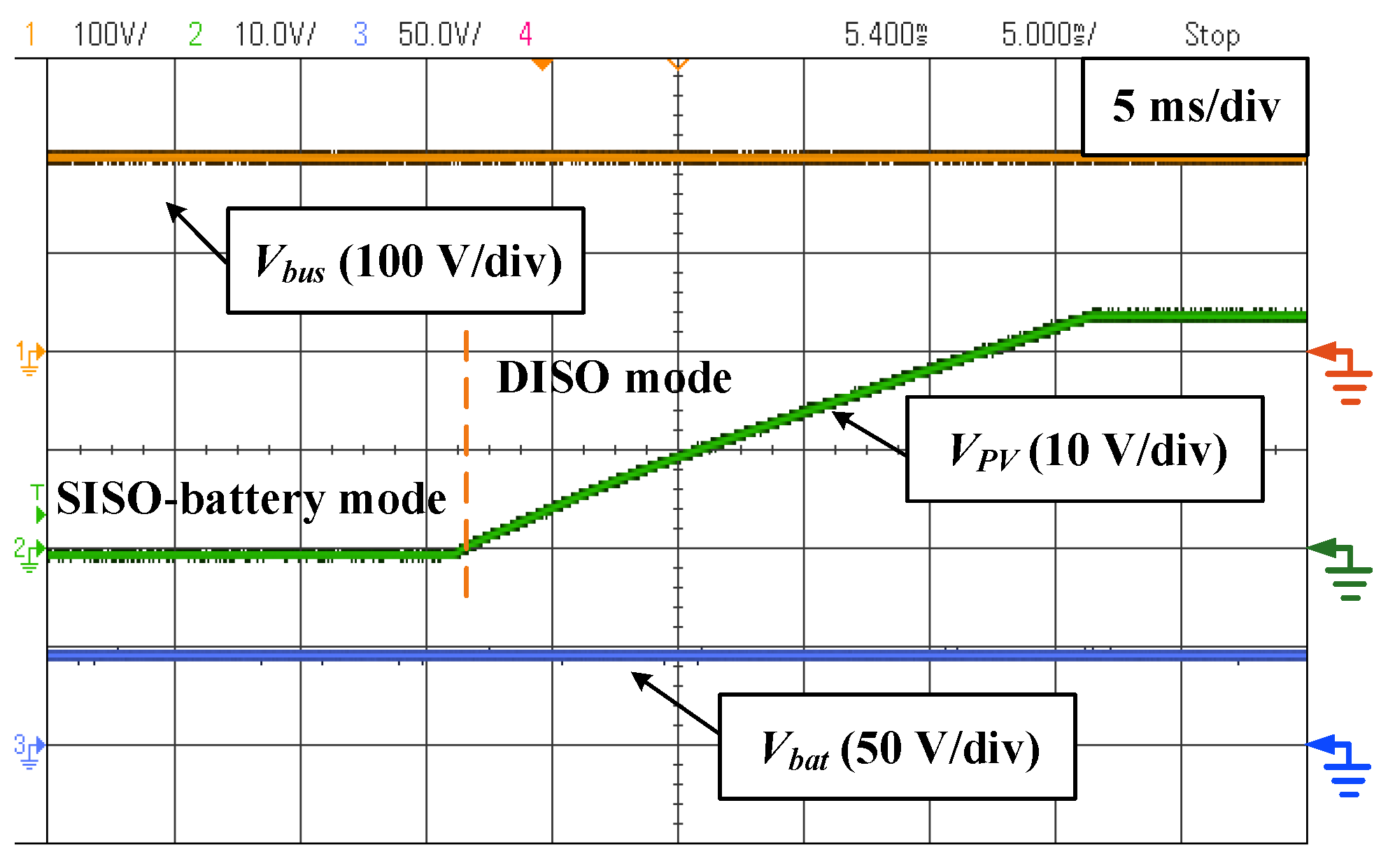
- Single input and single output for battery-energy providing (SISO-battery mode): As referred to in Figure 2b, only the battery discharges toward the DC bus. This mode works at night or during a rainy day;
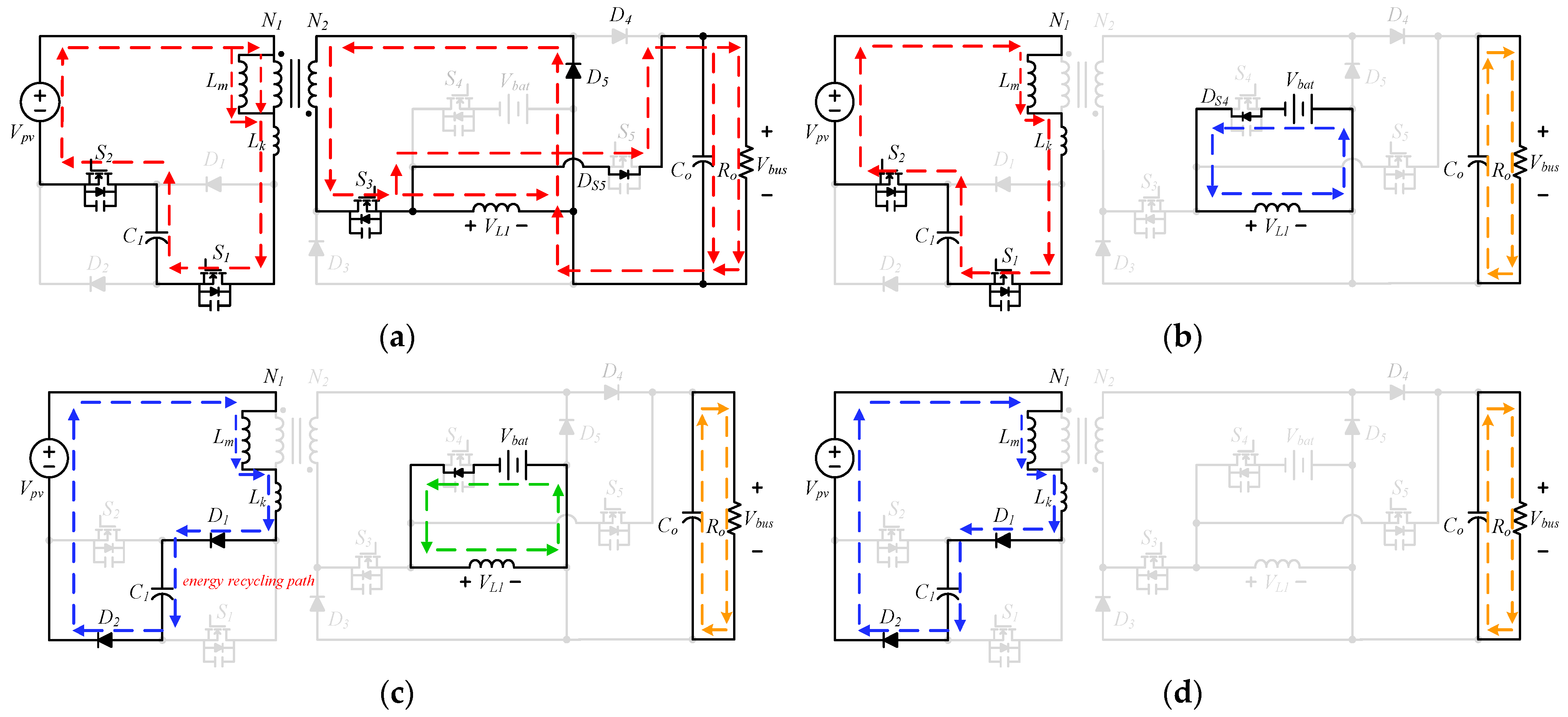
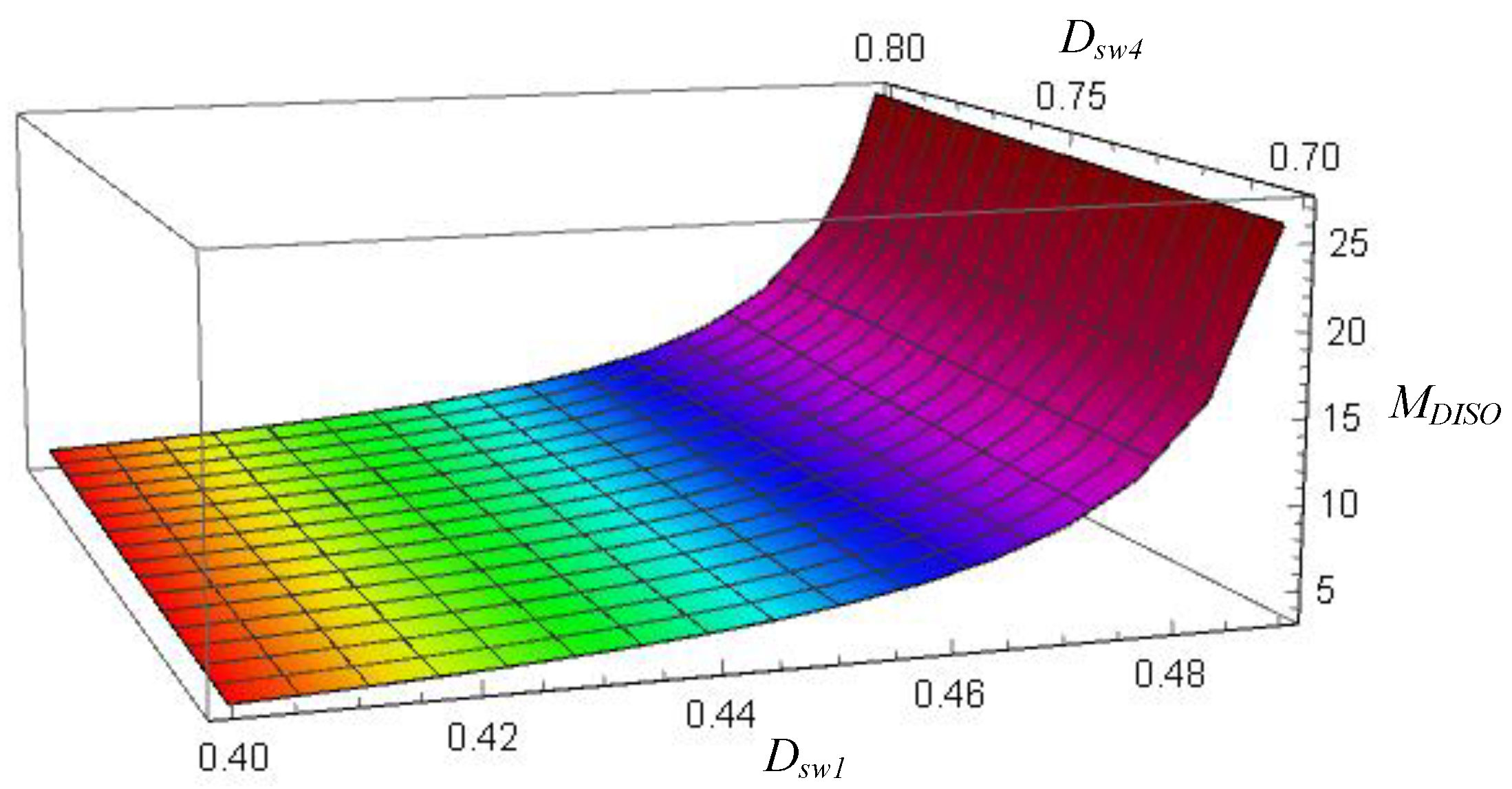
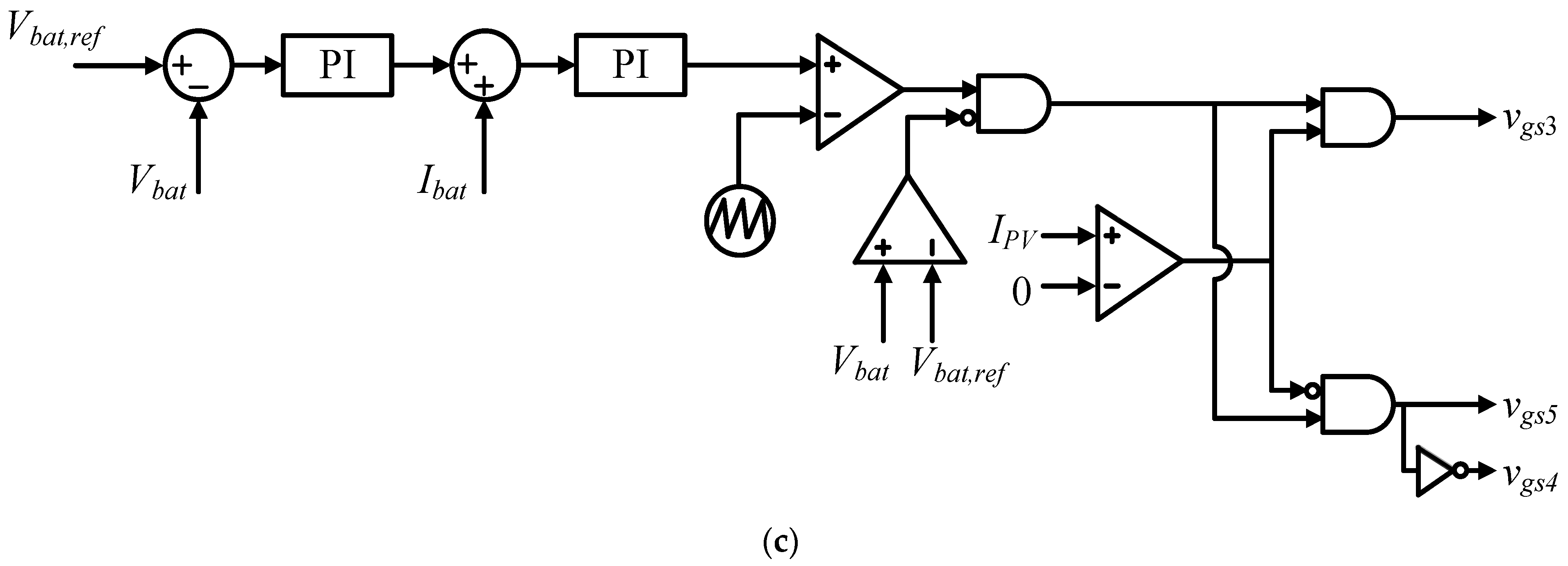
- Dual-input single-output mode (DISO mode): During the heavy-load period, the DC bus must draw sufficient power from the generation system. To meet the load demand, the PV panels and battery will provide energy simultaneously, which is illustrated in Figure 2c;
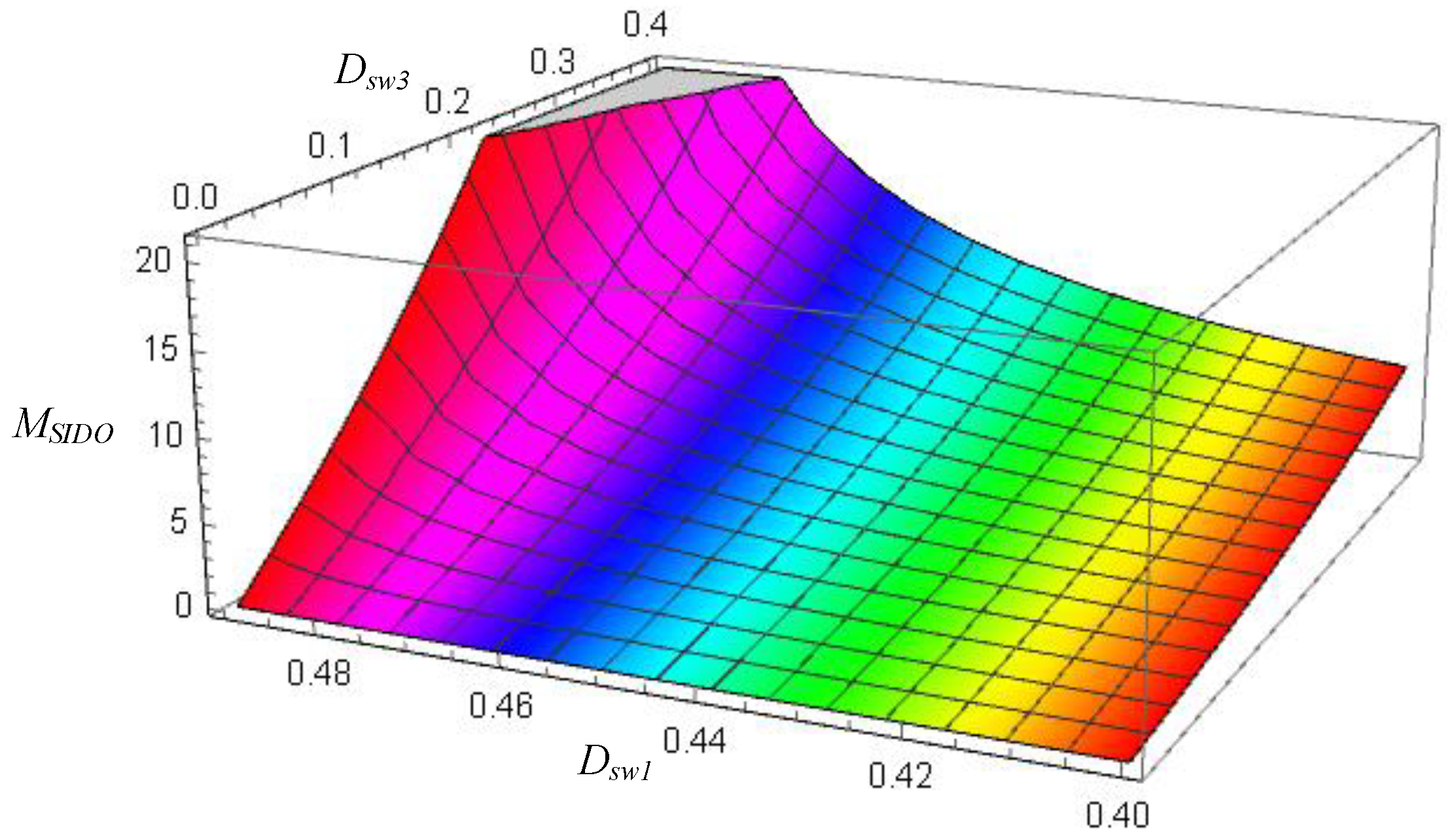
- Single-input dual-output mode (SIDO mode): The power flow is illustrated in Figure 2d. While in the period of intensive insolation, The PV panels can supply enough power to charge the battery and feed the DC bus as well;
- Back-feeding mode (BF mode): As shown in Figure 2e, under the operation of BF mode, the MPMDC can draw energy from the DC bus to charge the battery.
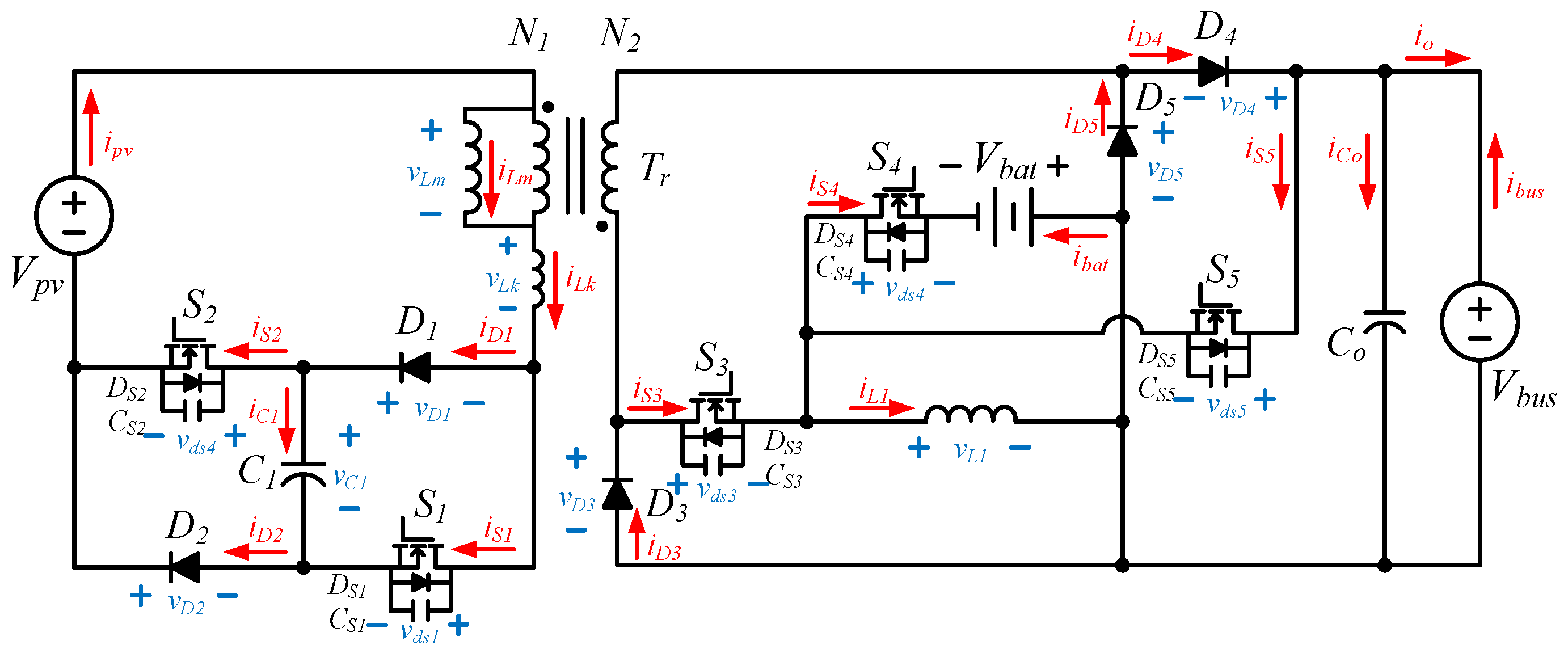
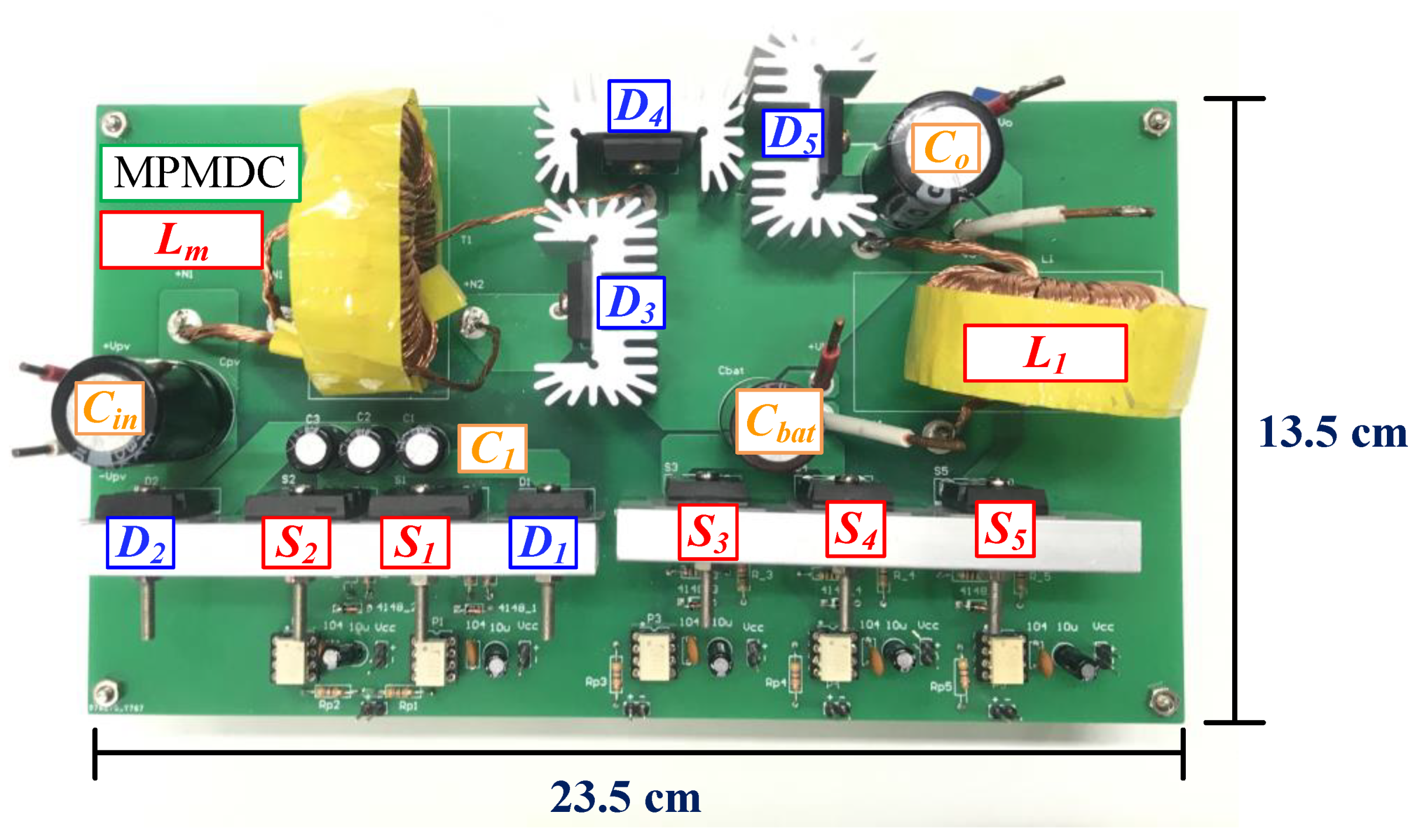
2. Converter Structure and Operation Analysis
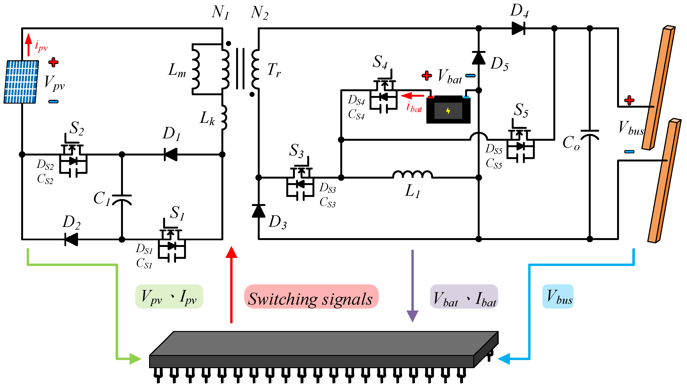
2.1. Operation Principle
- Capacitors C1 and C0 are large enough so that the voltage ripples on C1 and C0 can be neglected;
- The diodes D1–D5 are considered ideal;
- Parasitic capacitance in power switches is very small so that it can be reasonably omitted;
- The leakage inductance Lk is much smaller than the magnetizing inductance Lm;
- The duty ratios of switches S1 and S2 are all less than 0.5;
- The turns ratio of the transformer Tr is defined as n and equal to .
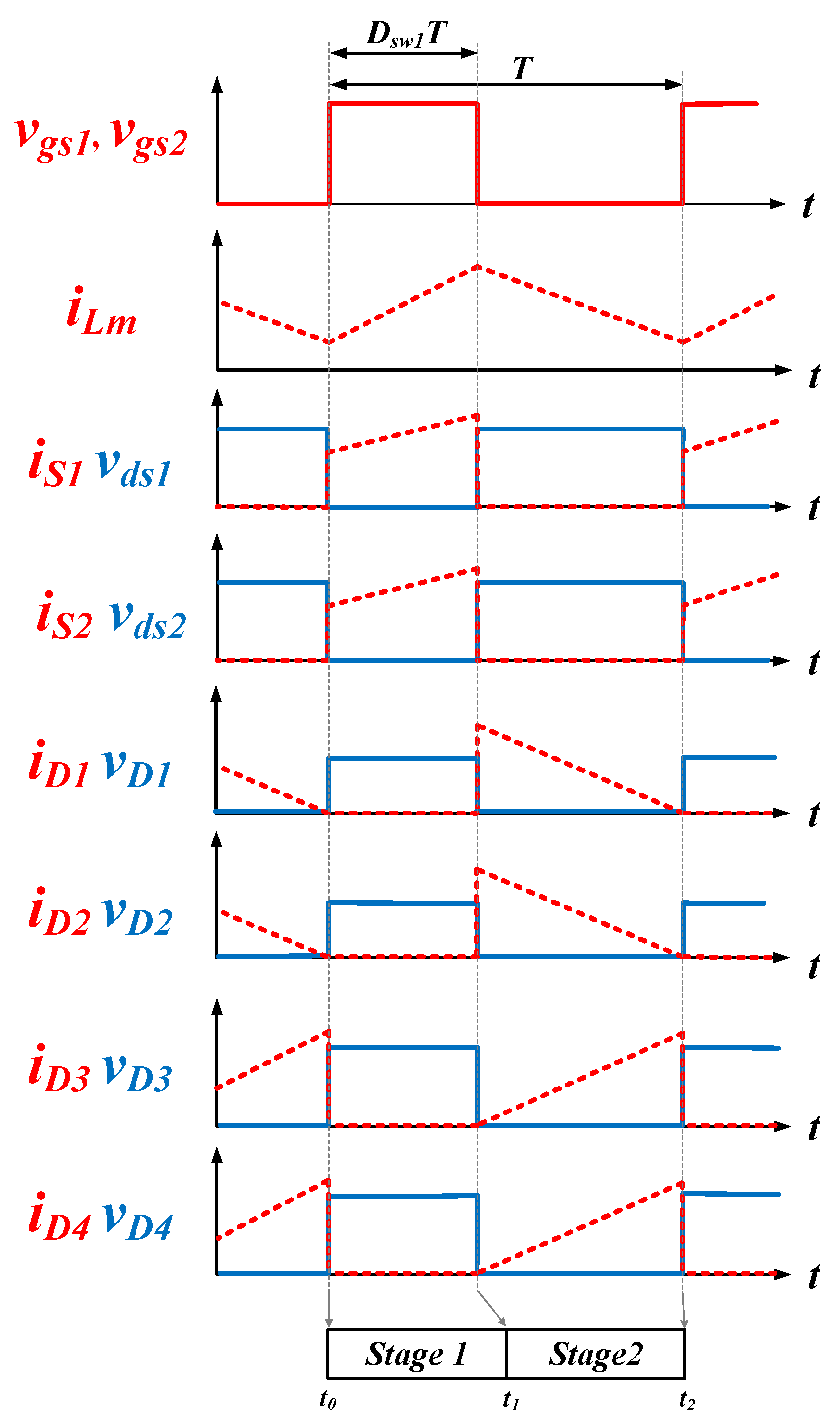
2.1.1. SISO-PV Mode
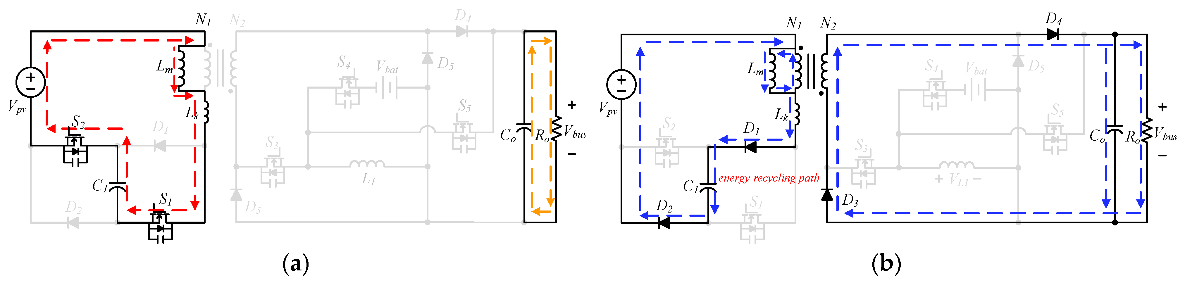
Stage 1 [t0–t1]
Stage 2 [t1–t2]
2.1.2. SISO-Battery Mode
Stage 1 [t0–t1]
Stage 2 [t1–t2]
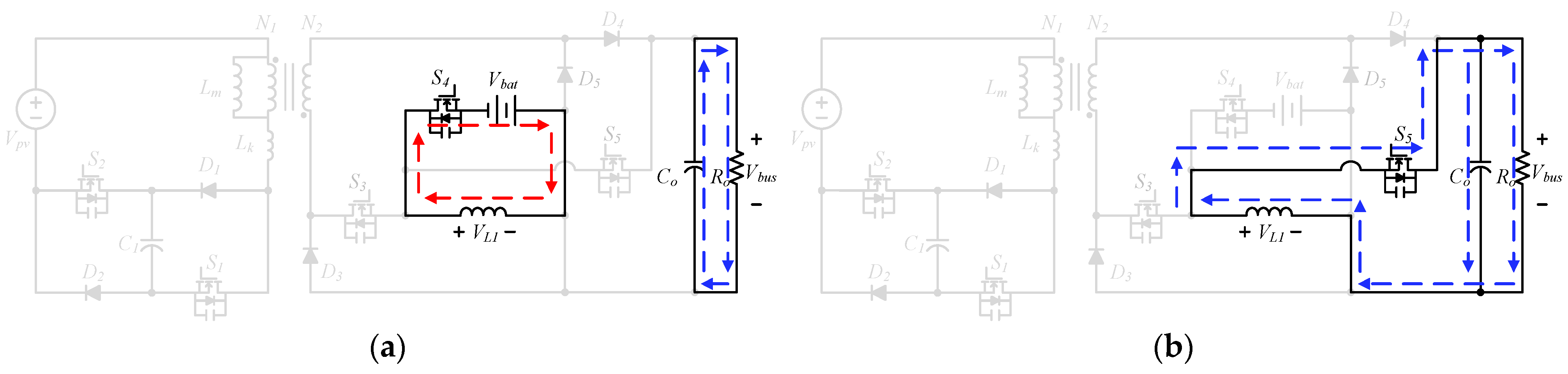
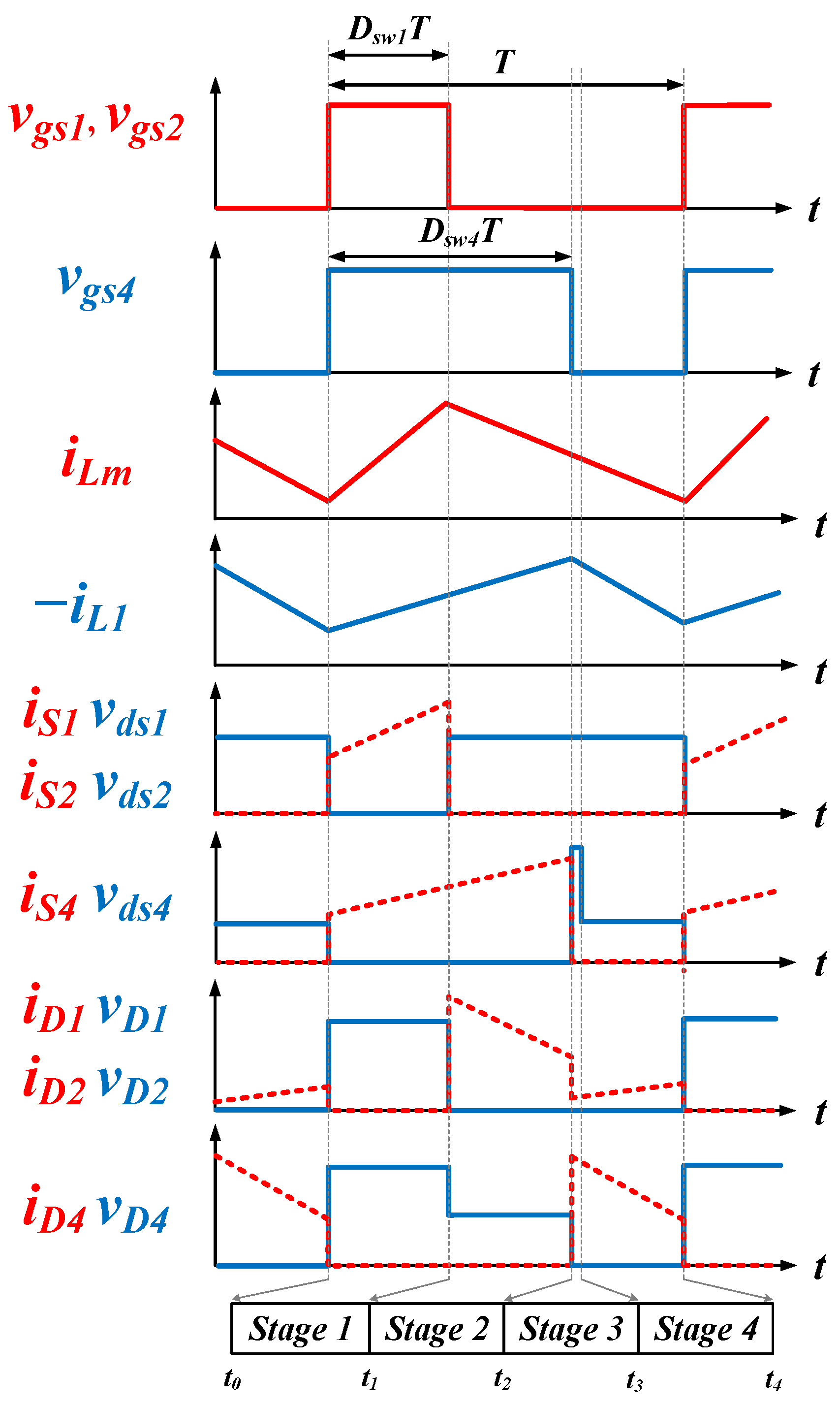
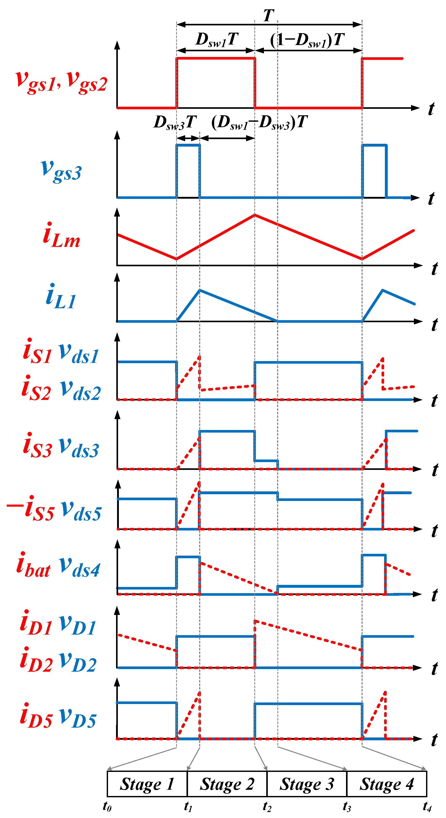
2.1.3. DISO Mode
Stage 1 [t0–t1]
Stage 2 [t1–t2]
Stage 3 [t2–t3]
Stage 4 [t3–t4]
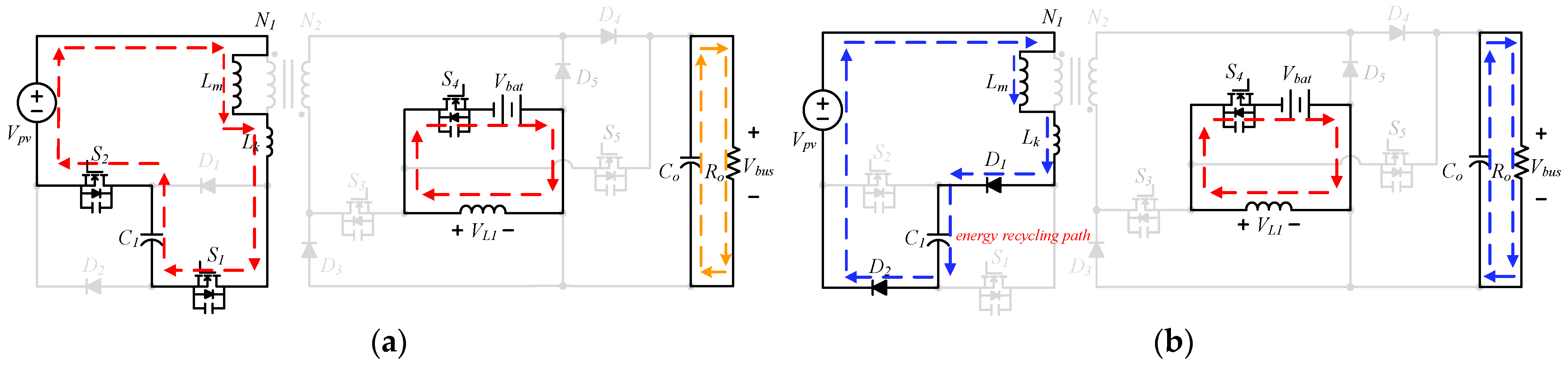
2.1.4. SIDO Mode
Stage 1 [t0–t1]
Stage 2 [t1–t2]
Stage 3 [t2–t3]
Stage 4 [t3–t4]
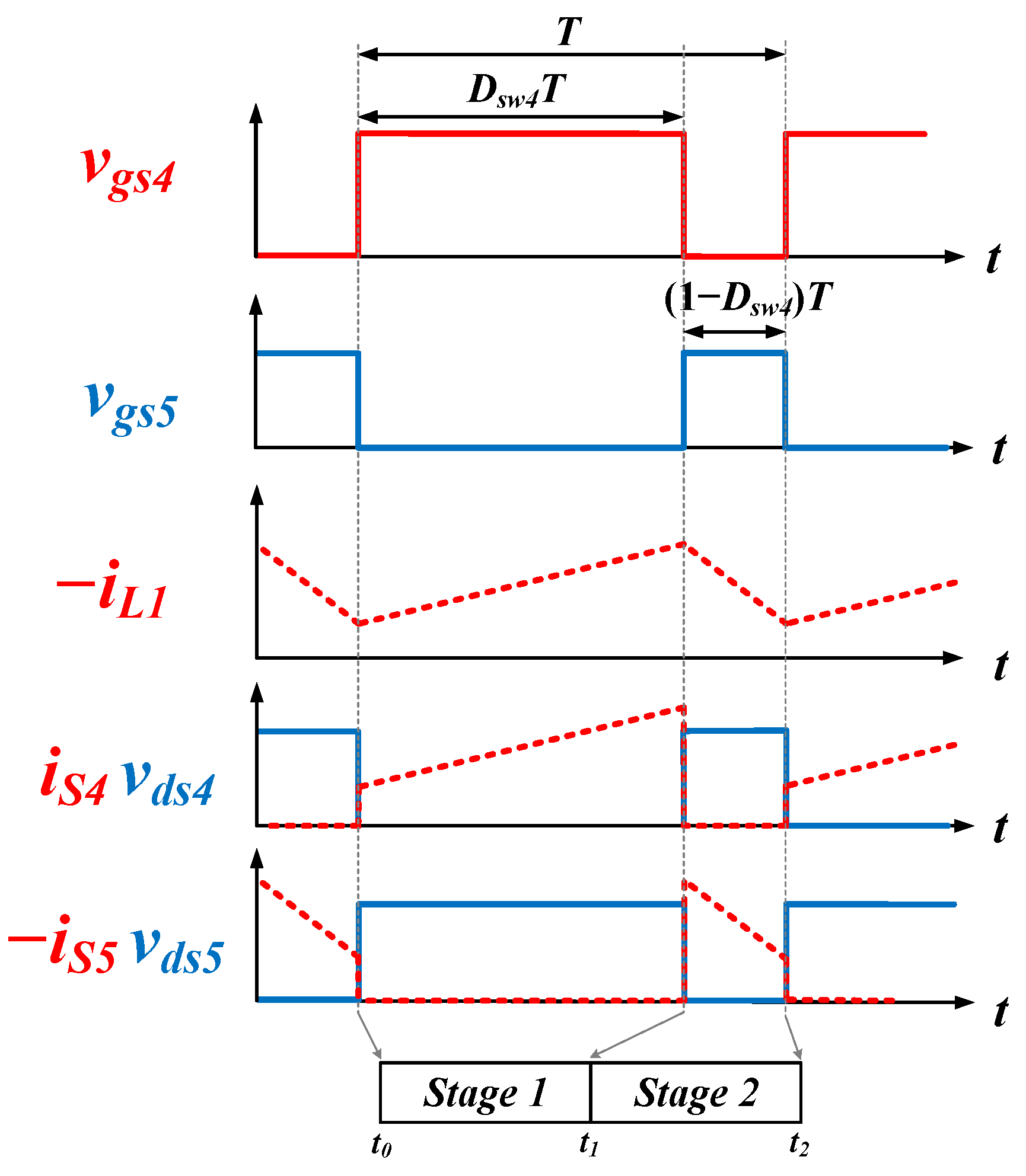
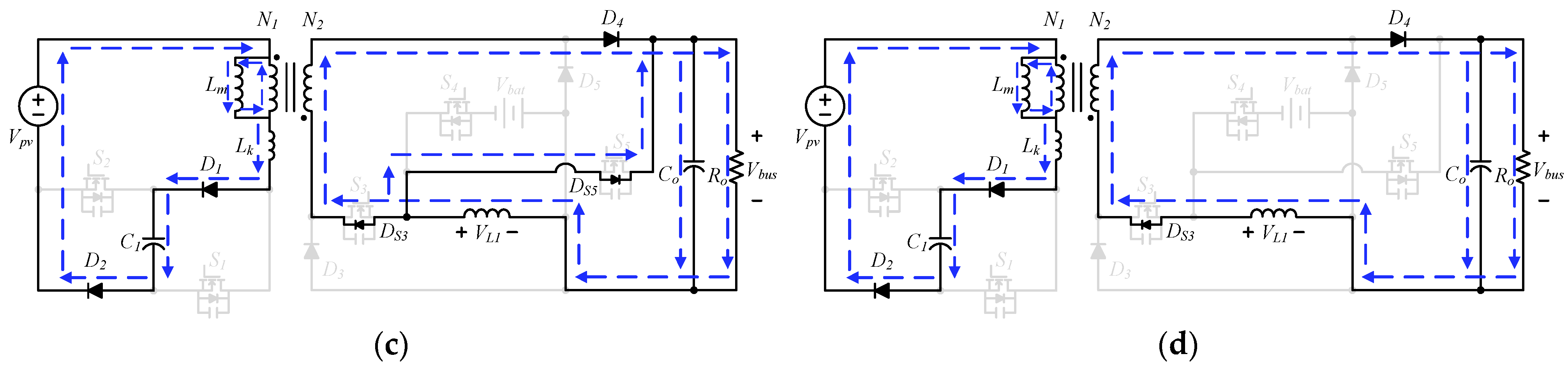
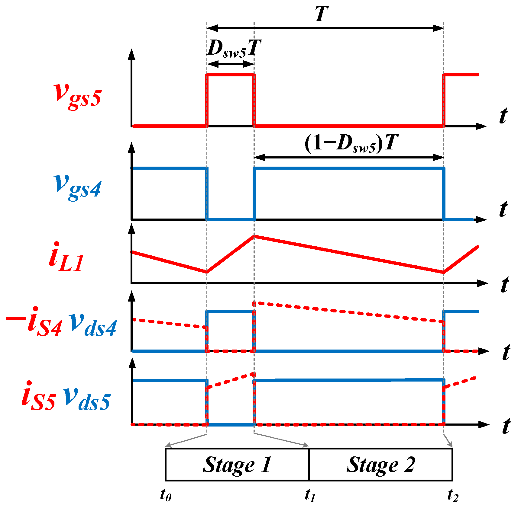
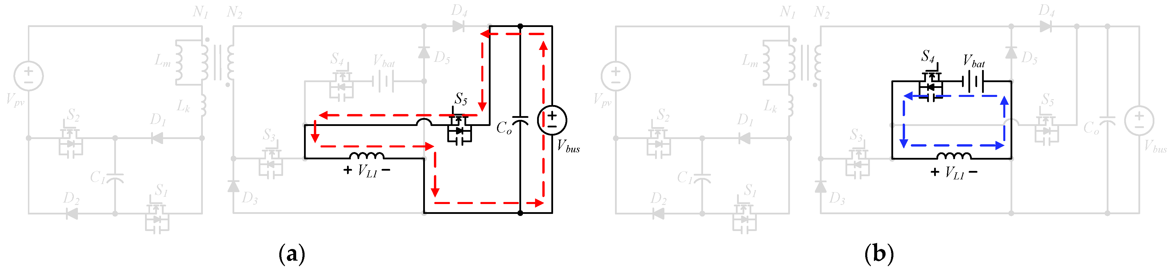
2.1.5. BF Mode
Stage 1 [t0–t1]
Stage 2 [t1–t2]
3. Steady-State Analysis
- All components are considered ideal;
- All the values of capacitors are large enough to keep their voltage constant during one switching cycle;
- The turns ratio of the transformer Tr is expressed as ;
- The Lm of the Tr and the inductor L1 both are operated in CCM.
3.1. Voltage Gain
3.1.1. Derivation for SISO-PV Mode
3.1.2. Derivation for SISO-Battery Mode
3.1.3. Derivation for DISO Mode
3.1.4. Derivation for SIDO Mode
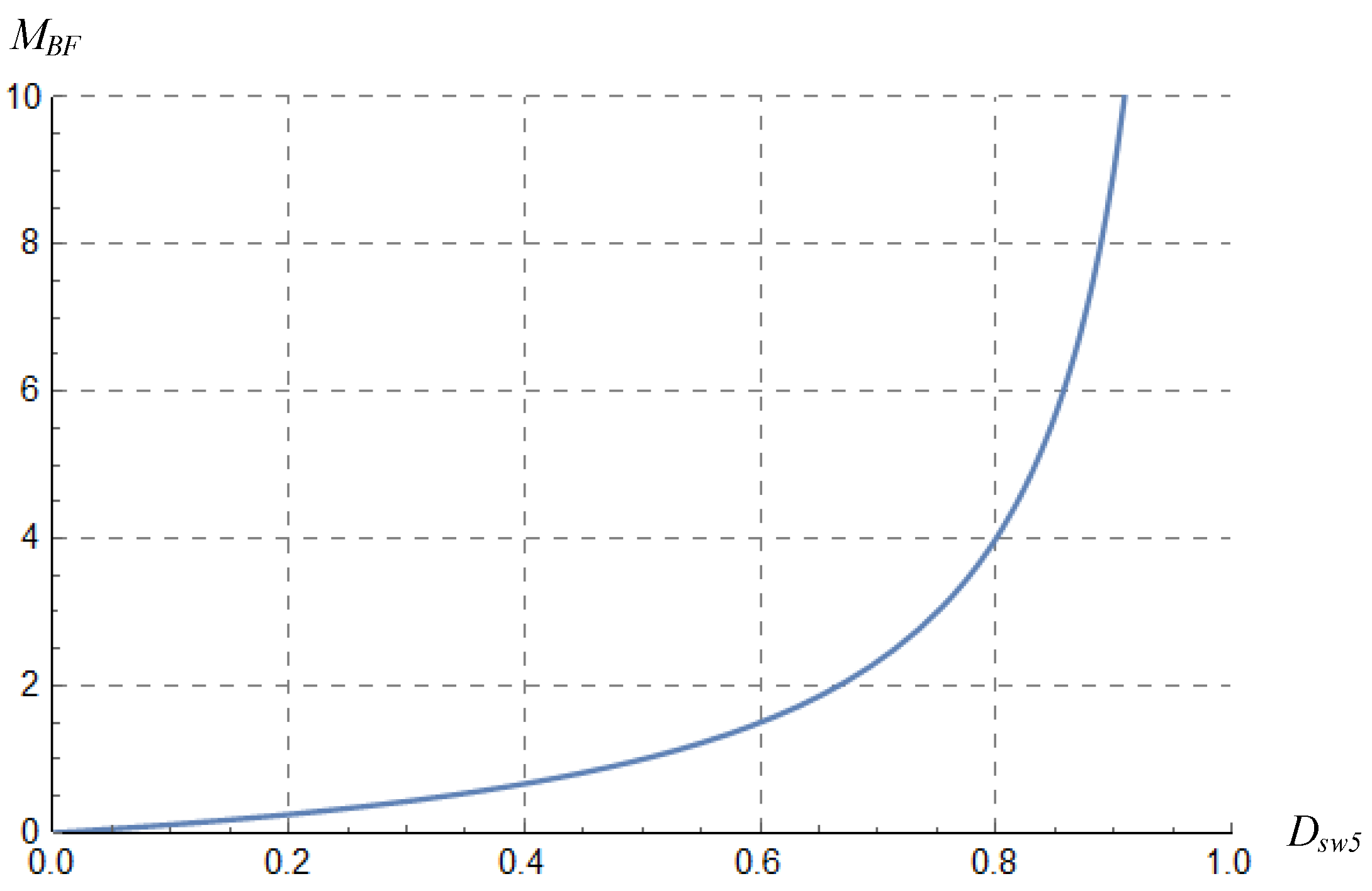
3.1.5. Derivation for BF Mode
3.2. Voltage Stresses on the Semiconductors
3.3. Current Stresses on the Semiconductors
3.4. Inductance Design
3.5. Capacitance Design
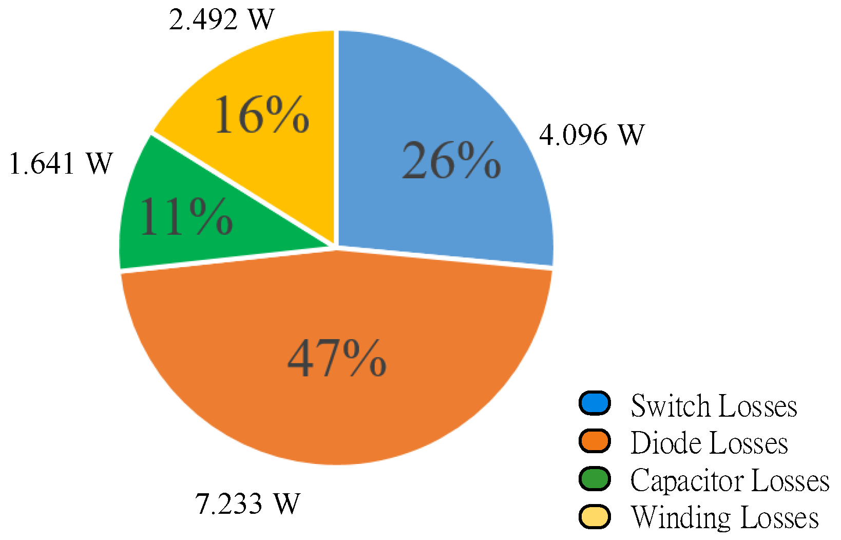
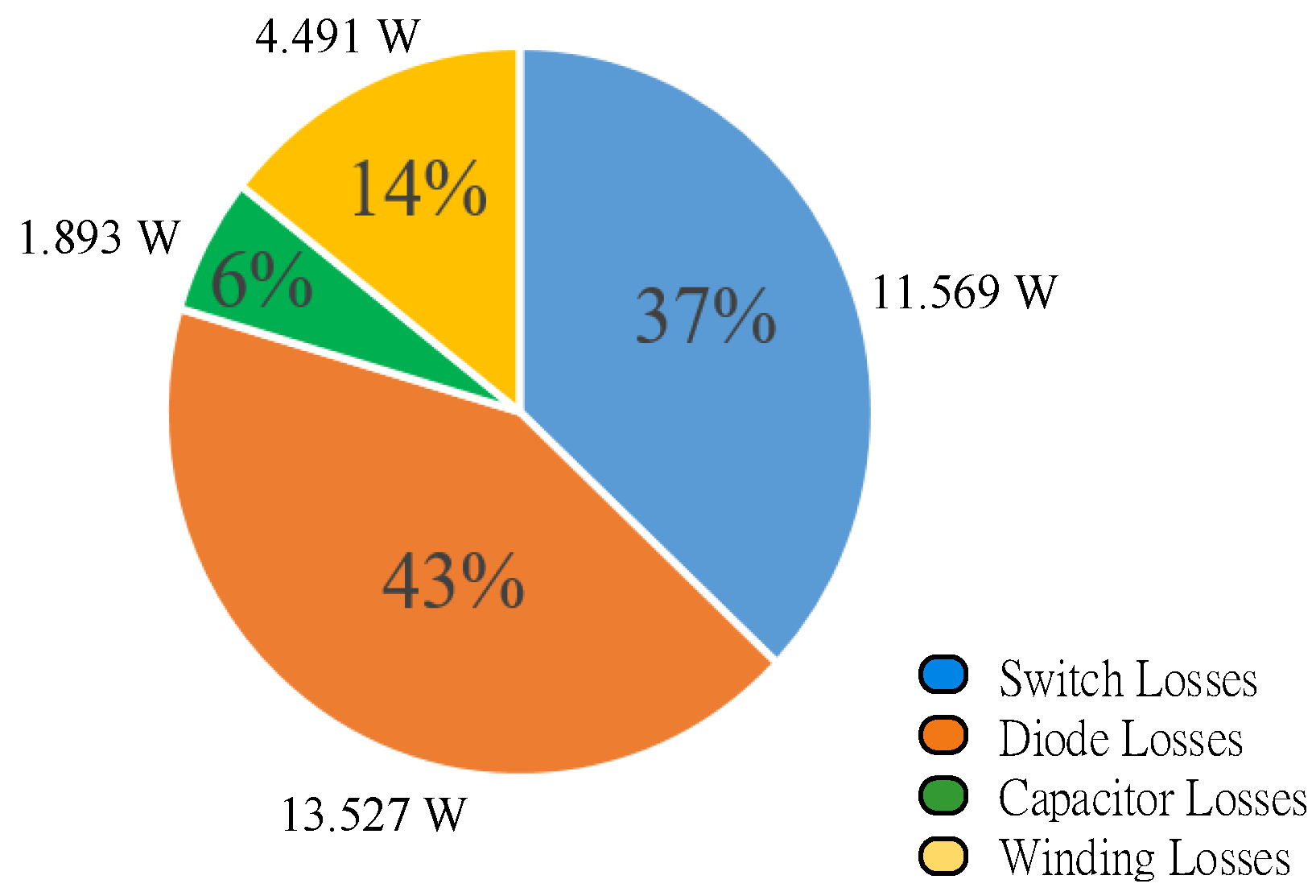
4. Experimental Results
4.1. SISO-PV Mode
4.2. SISO-Battery Mode
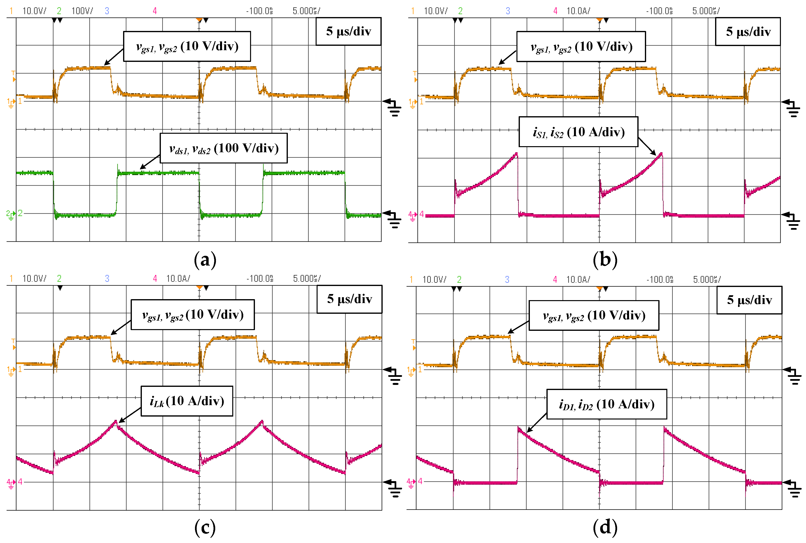
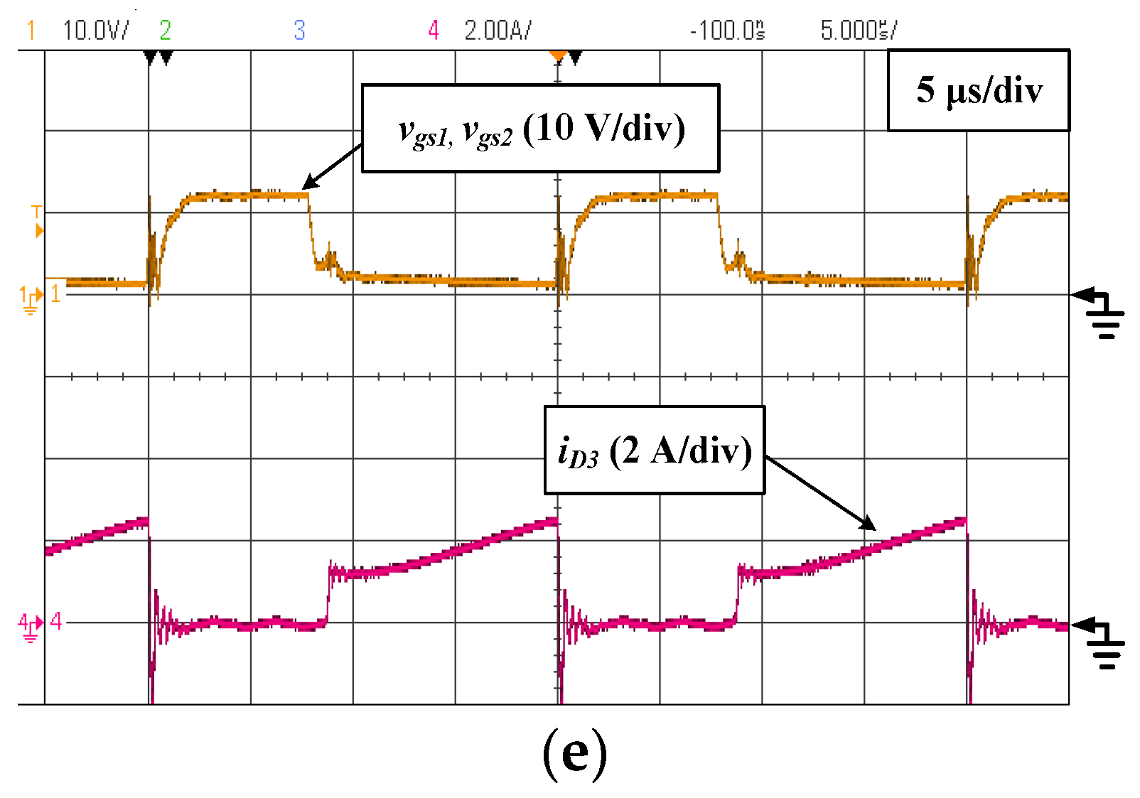
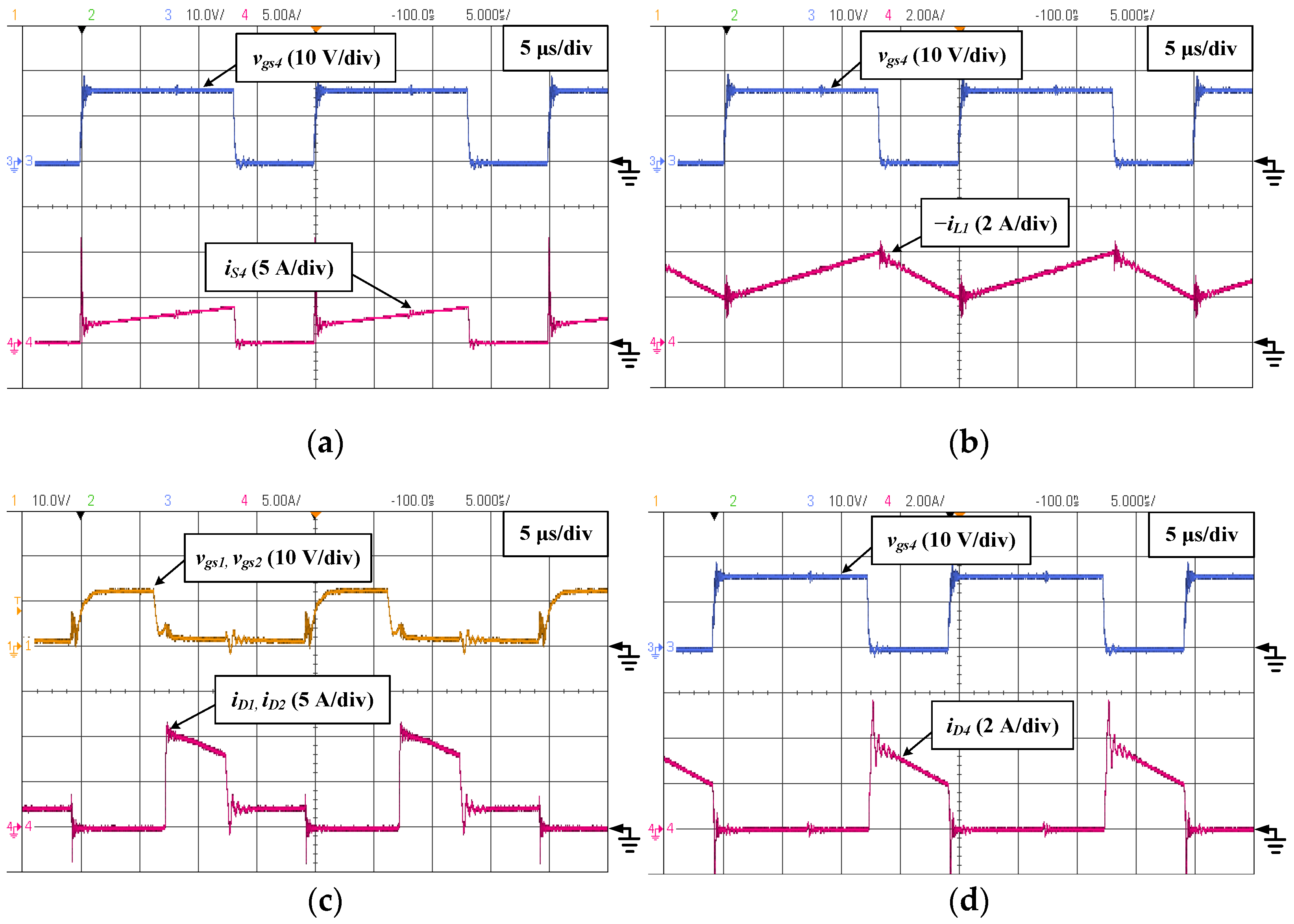
4.3. DISO Mode
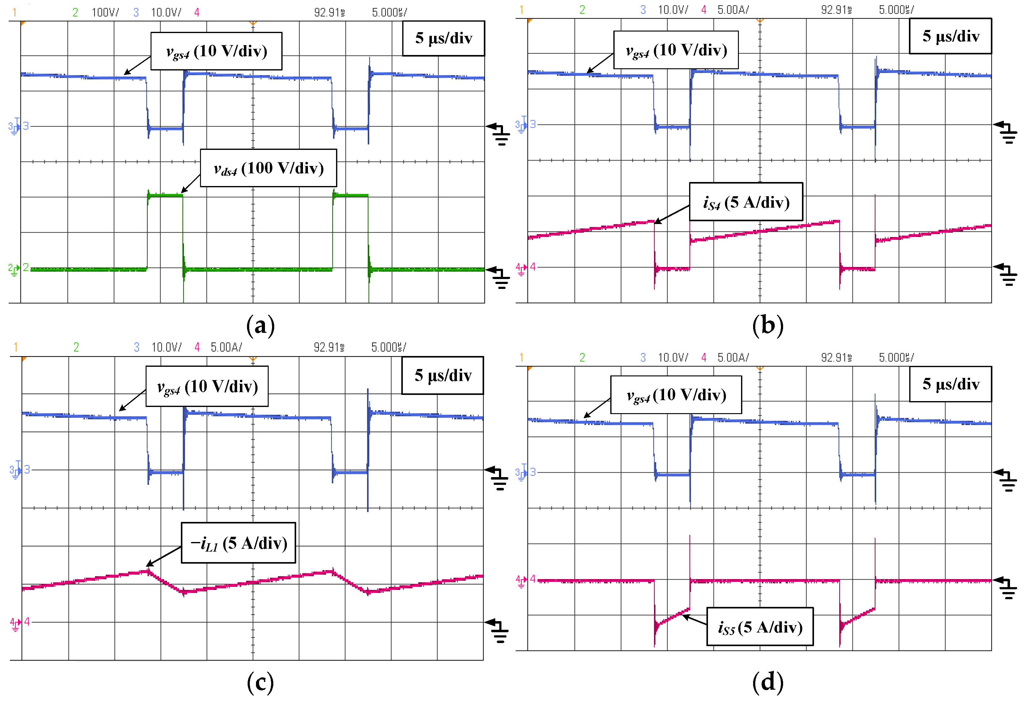
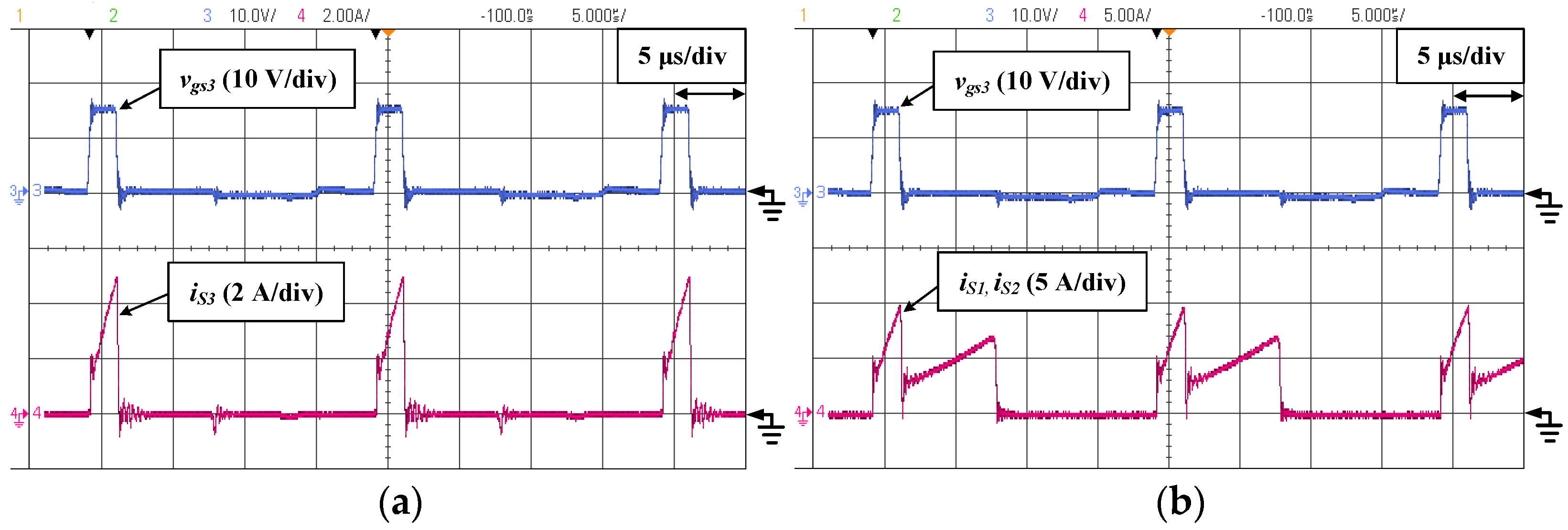
4.4. SIDO Mode
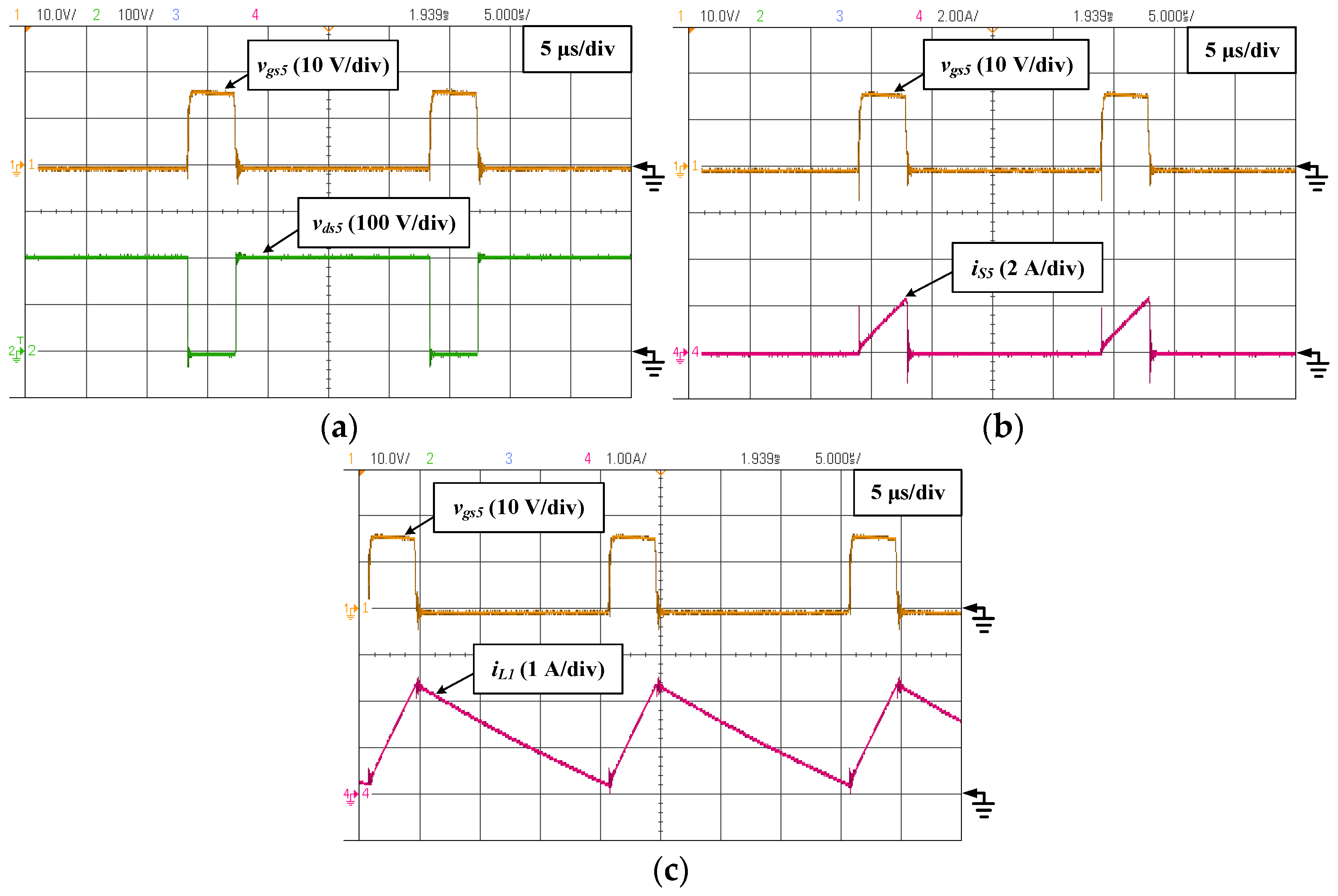
4.5. BF Mode
5. Performance Comparison
6. Conclusions
Author Contributions
Funding
Institutional Review Board Statement
Informed Consent Statement
Data Availability Statement
Conflicts of Interest
References
- Hasanpour, S.; Baghramian, A.; Mojallali, H. A modified SEPIC-based high step-up DC–DC converter with quasi-resonant operation for renewable energy applications. IEEE Trans. Ind. Electron. 2019, 66, 3539–3549. [Google Scholar] [CrossRef]
- Nouri, T.; Nouri, N.; Vosoughi, N. A novel high step-up high efficiency interleaved DC–DC converter with coupled inductor and built-in transformer for renewable energy systems. IEEE Trans. Ind. Electron. 2020, 67, 6505–6516. [Google Scholar] [CrossRef]
- Ramanathan; Girish, G.; Naomitsu, U. Non-isolated interleaved hybrid boost converter for renewable energy applications. Energies 2022, 15, 610. [Google Scholar] [CrossRef]
- Uno, M.; Sugiyama, K. Switched capacitor converter based multiport converter integrating bidirectional PWM and series-resonant converters for standalone photovoltaic systems. IEEE Trans. Power Electron. 2019, 34, 1394–1406. [Google Scholar] [CrossRef]
- Bizhani, H.; Noroozian, R.; Muyeen, S.M.; Blaabjerg, F. Wind farm grid integration architecture using unified expandable power converter. IEEE Trans. Power Electron. 2019, 34, 3407–3417. [Google Scholar] [CrossRef] [Green Version]
- Sikorski, A.; Falkowski, P.; Korzeniewski, M. Comparison of two power converter topologies in wind turbine system. Energies 2021, 14, 6574. [Google Scholar] [CrossRef]
- Chen, B.-Z.; Liao, H.; Chen, L.; Chen, J.-F. Design and implementation of the bidirectional DC-DC converter with rapid energy conversion. Energies 2022, 15, 898. [Google Scholar] [CrossRef]
- Hernandez, F.D.; Samanbakhsh, R.; Ibanez, F.M.; Martin, F. Self-balancing supercapacitor energy storage system based on a modular multilevel converter. Energies 2022, 15, 338. [Google Scholar] [CrossRef]
- Zhou, D.; Wang, J.; Li, Y.; Zou, J.; Sun, K. Model predictive power control of grid-connected quasi single-stage converters for high-efficiency low-voltage ESS integration. IEEE Trans. Ind. Electron. 2022, 69, 1124–1134. [Google Scholar] [CrossRef]
- Zhang, Y.; Liu, Q.; Gao, Y.; Li, J.; Sumner, M. Hybrid switched-capacitor/switched-quasi-Z-source bidirectional DC–DC converter with a wide voltage gain range for hybrid energy sources EVs. IEEE Trans. Ind. Electron. 2019, 66, 2680–2690. [Google Scholar] [CrossRef]
- Zhang, Y.; Gao, Y.; Zhou, L.; Sumner, M. A switched-capacitor bidirectional DC–DC converter with wide voltage gain range for electric vehicles with hybrid energy sources. IEEE Trans. Power Electron. 2018, 33, 9459–9469. [Google Scholar] [CrossRef]
- Yari, K.; Mojallali, H.; Shahalami, S.H. A New Coupled-inductor-based buck–boost DC–DC converter for PV applications. IEEE Trans. Power Electron. 2022, 37, 687–699. [Google Scholar] [CrossRef]
- Kanathipan, K.; Emamalipour, R.; Lam, J. A single-switch high-gain PV microconverter with low-switch-voltage-to-high-voltage-bus ratio. IEEE Trans. Power Electron. 2020, 35, 9530–9540. [Google Scholar] [CrossRef]
- Kumar, G.G.; Sundaramoorthy, K.; Karthikeyan, V.; Babaei, E. Switched capacitor–inductor network based ultra-gain DC–DC converter using single switch. IEEE Trans. Ind. Electron. 2020, 67, 10274–10283. [Google Scholar] [CrossRef]
- Santra, S.B.; Chatterjee, D.; Liang, T.J. High gain and high-efficiency bidirectional DC–DC converter with current sharing characteristics using coupled inductor. IEEE Trans. Power Electron. 2021, 36, 12819–12833. [Google Scholar] [CrossRef]
- Wang, Z.; Wang, P.; Li, B.; Ma, X.; Wang, P. A bidirectional DC–DC converter with high voltage conversion ratio and zero ripple current for battery energy storage system. IEEE Trans. Power Electron. 2021, 36, 8012–8027. [Google Scholar] [CrossRef]
- Yan, Y.-H.; Chang, Y.-N.; Peng, Z.-X. Design of a bidirectional CL3C full-bridge resonant converter for battery energy storage systems. Energies 2022, 15, 412. [Google Scholar] [CrossRef]
- Tian, Q.; Zhou, G.; Liu, R.; Zhang, X.; Leng, M. Topology synthesis of a family of integrated three-port converters for renewable energy system applications. IEEE Trans. Ind. Electron. 2021, 68, 5833–5846. [Google Scholar] [CrossRef]
- Chen, G.; Jin, Z.; Deng, Y.; He, X.; Qing, X. Principle and topology synthesis of integrated single-input dual-output and dual-input single-output DC–DC converters. IEEE Trans. Ind. Electron. 2018, 65, 3815–3825. [Google Scholar] [CrossRef]
- Rostami, S.; Abbasi, V.; Parastesh, M. Design and implementation of a multiport converter using Z-source converter. IEEE Trans. Ind. Electron. 2021, 68, 9731–9741. [Google Scholar] [CrossRef]
- Liang, T.J.; Liao, K.F.; Chen, K.H.; Chen, S.M. Three-port converter with single coupled inductor for high step-up applications. IEEE Trans. Power Electron. 2022, 37, 9840–9849. [Google Scholar] [CrossRef]
- Zhou, G.; Tian, Q.; Wang, L. Soft-switching high gain three-port converter based on coupled inductor for renewable energy system applications. IEEE Trans. Ind. Electron. 2022, 69, 1521–1536. [Google Scholar] [CrossRef]
- Aljarajreh, H.; Lu, D.D.-C.; Siwakoti, Y.P.; Tse, C.K.; See, K.W. Synthesis and analysis of three-port DC/DC converters with two bidirectional ports based on power flow graph technique. Energies 2021, 14, 5751. [Google Scholar] [CrossRef]
- Askarian, I.; Pahlevani, M.; Knight, A.M. Three-port bidirectional DC/DC converter for DC nanogrids. IEEE Trans. Power Electron. 2021, 36, 8000–8011. [Google Scholar] [CrossRef]
- Faraji, R.; Ding, L.; Esteki, M.; Mazloum, N.; Khajehoddin, S.A. Soft-switched single inductor single stage multiport bidirectional power converter for hybrid energy systems. IEEE Trans. Power Electron. 2021, 36, 11298–11315. [Google Scholar] [CrossRef]
- Aljarajreh, H.; Lu, D.D.C.; Siwakoti, Y.P.; Tse, C.K. A nonisolated three-port DC–DC converter with two bidirectional ports and fewer components. IEEE Tran. Power Electron. 2022, 37, 8207–8216. [Google Scholar] [CrossRef]
- Danyali, S.; Moradkhani, A.; Aazami, R.; Haghi, M. New dual-input zero-voltage switching DC–DC boost converter for low-power clean energy applications. IEEE Trans. Power Electron. 2021, 36, 11532–11542. [Google Scholar] [CrossRef]
- Wang, K.; Liu, W.; Wu, F. Topology-level power decoupling three-port isolated current-fed resonant DC-DC converter. IEEE Trans. Ind. Electron. 2022, 69, 4859–4868. [Google Scholar] [CrossRef]
- Dobakhshari, S.S.; Fathi, S.H.; Milimonfared, J. A new soft-switched three-port DC/DC converter with high voltage gain and reduced number of semiconductors for hybrid energy applications. IEEE Trans. Power Electron. 2020, 35, 3590–3600. [Google Scholar] [CrossRef]
- Deng, J.; Wang, H.; Shang, M. A ZVS three-port DC/DC converter for high-voltage bus-based photovoltaic systems. IEEE Trans. Power Electron. 2019, 34, 10688–10699. [Google Scholar] [CrossRef]
- Qian, T.; Guo, K.; Qian, C. A combined three-port LLC structure for adaptive power flow adjustment of PV systems. IEEE Trans. Power Electron. 2020, 35, 10413–10422. [Google Scholar] [CrossRef]
- Jakka, V.N.S.R.; Shukla, A.; Demetriades, G.D. Dual-transformer-based asymmetrical triple-port active bridge (DT-ATAB) isolated DC–DC converter. IEEE Trans. Ind. Electron. 2017, 64, 4549–4560. [Google Scholar] [CrossRef]
- Shen, C.-L.; Chen, L.-Z.; Chen, H.-Y. Dual-input isolated DC-DC converter with ultra-high step-up ability based on sheppard taylor circuit. Electronics 2019, 8, 1125. [Google Scholar] [CrossRef] [Green Version]


| Mode | Voltage Gain |
|---|---|
| SISO-PV mode | |
| SISO-battery mode | |
| DISO mode | |
| SIDO mode | |
| BF mode |
| Parameters | Values & Specifications |
|---|---|
| Pbus (DC-bus power) | 200 W |
| Pbat (Battery power) | 50 W |
| Vbus (DC-bus voltage) | 200 V |
| Vpv (PV voltage) | 24 V |
| Vbat (Battery voltage) | 48 V |
| fs (Switch frequency) | 50 kHz |
| L1 (Inductance) | 300 μH |
| Lm (Magnetizing inductance) | 270 μH |
| Lk (Leakage inductance) | 3.6 μH |
| S1 and S2 (Power MOSFET) | IXTK90N25L2 (250 V/90 A) |
| S3, S4 and S5 (Power MOSFET) | IXFH36N50P (500 V/36 A) |
| D1 and D2 (Diodes) | DSSK 60-02A (200 V/2 × 30 A) |
| D3, D4 and D5 (Diodes) | DPG60C300HB (300 V/2 × 30 A) |
| C1 (Electrolytic capacitor) | 3 × 10 μF |
| Co (Electrolytic capacitor) | 100 μF |
| Cbat (Electrolytic capacitor) | 68 μF |
| n (Transformer turns ratio) | 43:65 |
| Ref. | [21] | [29] | [30] | [31] | Proposed |
|---|---|---|---|---|---|
| Input voltage | 60 V | 30 V | 20–40 V | 50 V | 24 V |
| Battery voltage | 72 V | 24 V | 60 V | 50 V | 48 V |
| Output voltage | 200 V | 400 V | 760 V | 100 V | 200 V |
| Rated power | 600 W | 200 W | 500 W | 1000 W | 200 W |
| MOSFETs | 12 | 3 | 6 | 14 | 5 |
| Diodes | 0 | 3 | 4 | 0 | 5 |
| Capacitors | 3 | 6 | 8 | 1 | 3 |
| Magnetic elements | 5 | 4 | 3 | 2 | 2 |
| Operational mode | 4 | 3 | 2 | 2 | 5 |
| Turns ratio (n) | 2 | 5 | 2 | 2 | 1.5 |
| Isolation | Yes | Yes | Yes | Yes | Yes |
| Leakage energy recycling | No | Yes | No | Yes | Yes |
| Voltage gain (bus voltage) |
Publisher’s Note: MDPI stays neutral with regard to jurisdictional claims in published maps and institutional affiliations. |
© 2022 by the authors. Licensee MDPI, Basel, Switzerland. This article is an open access article distributed under the terms and conditions of the Creative Commons Attribution (CC BY) license (https://creativecommons.org/licenses/by/4.0/).
Share and Cite
Shen, C.-L.; Chen, L.-Z.; Chen, G.-Y.; Yang, C.-M. Multi-Port Multi-Directional Converter with Multi-Mode Operation and Leakage Energy Recycling for Green Energy Processing. Energies 2022, 15, 5629. https://0-doi-org.brum.beds.ac.uk/10.3390/en15155629
Shen C-L, Chen L-Z, Chen G-Y, Yang C-M. Multi-Port Multi-Directional Converter with Multi-Mode Operation and Leakage Energy Recycling for Green Energy Processing. Energies. 2022; 15(15):5629. https://0-doi-org.brum.beds.ac.uk/10.3390/en15155629
Chicago/Turabian StyleShen, Chih-Lung, Li-Zhong Chen, Guan-Yu Chen, and Ching-Ming Yang. 2022. "Multi-Port Multi-Directional Converter with Multi-Mode Operation and Leakage Energy Recycling for Green Energy Processing" Energies 15, no. 15: 5629. https://0-doi-org.brum.beds.ac.uk/10.3390/en15155629