

Inductively Powered Sensornode Transmitter Based on the Interconnection of a Colpitts and a Parallel Resonant LC Oscillator

Institute of Measurement and Sensor Technology, UMIT TIROL—Private University for Health Sciences and Health Technology, Eduard-Wallnöfer-Zentrum 1, 6060 Hall in Tirol, Austria
*
Author to whom correspondence should be addressed.
Energies 2022, 15(17), 6198; https://0-doi-org.brum.beds.ac.uk/10.3390/en15176198
Submission received: 6 July 2022
/
Revised: 16 August 2022
/
Accepted: 22 August 2022
/
Published: 25 August 2022
(This article belongs to the Special Issue Distributed Wireless Sensors and Power Transfer)
Abstract
:An inductively powered passive transmitter architecture for wireless sensornodes is presented in this paper. The intended applications are inductively powered internally illuminated photoreactors. The application range of photoreactors is wide. They are used, e.g., for microalgae cultivation or for photochemistry, just to name two important fields of use. The inductive powering system used to transmit energy to the wireless internal illumination system is to be additionally used to supply the here presented transmitter. The aim of expanding the named internal illuminated photoreactors with wireless sensors is to obtain a better insight into the processes inside it. This will be achieved by measuring essential parameters such as, e.g., the temperature, pH value, or gas concentrations of the medium inside the reactor, which for algal cultivation would be water. Due to the passive architecture of the transmitter electronics, there is no need for batteries, and therefore, no temporal limitations in their operational cycle are given. The data transmission is also implemented using the inductive layer in the low frequency range. The data transmitting coil and the energy receive coil are implemented as one and the same coil in order to avoid interference and unwanted couplings between them, and in order to save weight and space. Additionally, the transmitter works in a two-step alternating cycle: the energy harvesting step, followed by the data transmission step. The measured values are sent using on-off keying. Therefore, a Colpitts oscillator is switched on and off. The circuit is simulated using SPICE simulations and consequentially implemented as a prototype in order to perform practical analyses and measurements. The feasibility of our transmitter is therefore shown with the performed circuit simulations, and practically, by testing our prototype on an internal illuminated laboratory scaled photoreactor.
1. Introduction
1.1. Motivation and Context
Inductive data and power transmission are gaining a lot of interest and application fields in the last decades [1,2]. Wireless power transmission in general is used in a variety of devices, e.g., wireless charging systems for consumer electronics like mobile phones or toothbrushes [2,3], or for electrical vehicles enabling their charging with no physical connection [4]. Since the 1960s, inductive power transfer has been used in various implantable devices [5], whereas the recommended frequencies are in the range of kHz to MHz [6]. Generally, in order to power battery-free devices, inductive power transmission is a reliable method for supplying a continuous availability of energy [7]. Other important application areas for the use of wireless power transfer are e.g., moving parts or sealed applications, and it can also be used as an additional supply where alternative sources can be interrupted [8]. The goal of our research is to expand internally illuminated photoreactors with wireless sensornodes in order to enable a better monitoring of the processes inside them. The advantages of a passive and wireless functionality are clear: the operating time is not limited by a battery lifetime, and no cables and cable guides are needed. In this paper, we therefore present a design for realizing the transmitter electronics for a battery-free wireless sensornode that uses wireless inductive power transmission as an energy supply and the inductive data transmission for sending the measured data. Our system is conceived for use in the internally illuminated photoreactors presented in [9,10,11]. Those photoreactors already use inductive wireless power transmission for powering their internal illumination. We use this system additionally for powering our wireless sensornodes. The particularity of the presented design is the fact that the same coil is used to inductively receive the energy, as well as for sending the sensed data. This is realized through an interconnection of two oscillators with different resonant frequencies, whereas the commonly used coil represents a shared component of these two circuits. The topic of wireless sensornodes for similar applications is also researched by others: There is a similar project where wirelesses spherical sensors are used to measure the temperature inside biotechnological applications. Those wireless sensors are battery powered and they use the 433 MHz frequency band to send the measured data to a base station. The battery inside those wireless sensornodes is wirelessly charged in a charging station [12]. The authors of [13] are working on locatable autonomous dataloggers in order to enable distributed measurements in industrial applications such as, e.g., tanks used for fermentation [13].
1.2. Structure of the Paper
This paper has the following structure: in Section 2, a short overview on inductively powered internal illuminated photoreactors and the constraints for our system are given. The transmitter architecture is presented in Section 3, where the circuit used in this study is introduced, as well as relevant transfer functions. A crucial point thereby is the interconnection of the two oscillators used. Section 4 shows the results of the performed SPICE simulations, as well as the measurement results on the transmitter prototype. The conclusion and outlook are given in Section 5 and Section 6.
2. Locatable Wireless Sensors for Internally Illuminated Photoreactors
The long-term aim of this research is to expand the internal illumination system presented in [9,10,11] with locatable wireless sensors, in order to allow a better insight into the processes inside the reactor. The sensornode therefore needs a wireless power receiving unit that takes the energy provided by an inductive power supply in order to supply the whole transmitter. The authors of [10] presented the class-E amplifier used for the inductive power transfer to loosely coupled so-called Wireless Light Emitters (WLE) in photoreactors. The driving coils used to generate the magnetic field are placed at the outer diameter of the photoreactor, and the amplifier is tuned to approx. 180 kHz. Our sensornode will use a modified LC parallel resonant circuit tuned to this frequency, and the energy gained from the wireless power transfer is temporarily stored in a capacitor. The stored energy is used in a second step for powering the sensor and sending its sensed data.
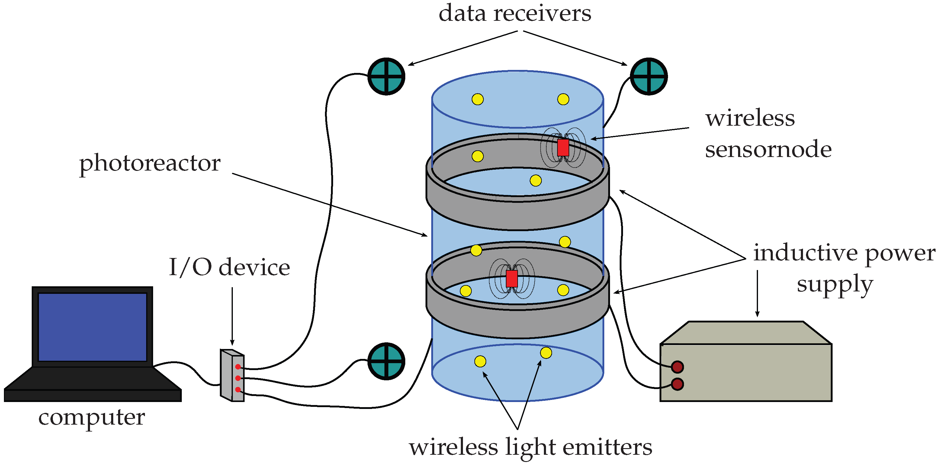
In [14]—Section 2, we already investigated the data transmission methods for an underwater environment, as is the case for water-/seawater-filled photoreactors. Based on those investigations, we also use the inductive principle based on low frequencies for the data transmission. The transmitter presented here therefore needs a second oscillator that is tuned to another resonant frequency in order to inductively send back the measured data. A methodology for locating the wireless sensornode by measuring the magnetic field of its transmitting coil at different positions was also presented in [14] and tested for air as the surrounding media on a setup with a simple oscillator as a transmitter and two triaxial receivers. Figure 1 shows the conceptualization of our system, where our wireless sensors will be placed together with the WLEs inside the photoreactor and are also supplied by the same inductive power supply. The signals sensed by the triaxial receivers are digitalized using an I/O device in order to enable further data processing on the computer, such as e.g., the localization of the sensornode, or for decoding the measured values. In this paper, the focus is set to the electrical architecture of the transmitter circuit for a single wireless sensornode.
3. Transmitter Architecture
The transmitter presented in this paper is conceived to obtain the necessary energy from the magnetic field generated by the inductive power supply presented in [10]. The stored energy is used in a second step for powering the sensor and for sending the measured data to the outside of the reactor. A crucial point of our considerations was the realization of a transmitter that uses the same transmitter coil for the wireless power transfer (WPT), and for sending the sensed data. This is performed in order to avoid interference between a WPT- and a data transmitting coil in advance. Therefore, the data transmission circuit and the energy receive circuit need to be linked together in order to enable this constraint. We use a LC parallel resonant circuit architecture as an energy receiver, and a Colpitts oscillator as a transmitter circuit. The chosen data modulation technique is the on-off keying. This simplifies the realization of the data transmission hardware; the Colpitts oscillator just needs to be switched on and off. The resonant frequency of the energy receive circuit is defined by the frequency of the named inductive energy supply, 180 kHz. The data transmission frequency, on the other hand, is set at a factor of 1.66 higher, at approx. 300 kHz. Our consideration behind this choice was to avoid interference caused by harmonics.
3.1. Circuit Design and Calculations
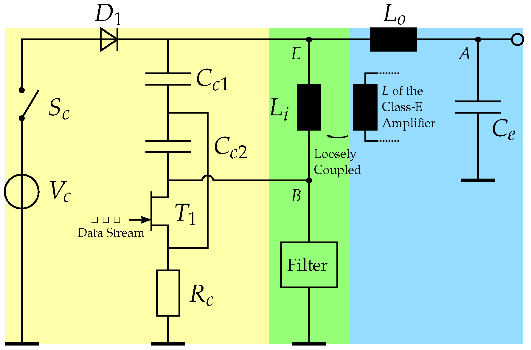
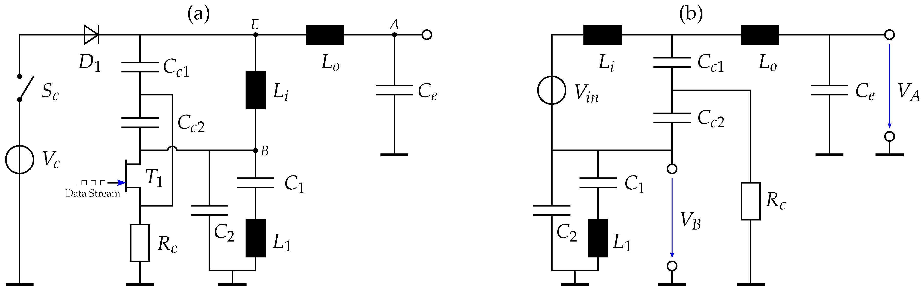
The centerpiece of the presented transmitter is the interconnection of the data transmission circuit, which is a Colpitts oscillator, and the WPT receive circuit, which is a LC parallel resonant circuit. The circuits are linked together using one single transmitter coil, which is an air core coil. Of course, the whole circuit includes more than one inductance. However, only the coil that is used to link the two oscillator circuits is designed as an air core coil, in order to use it as an antenna to transmit the data, and for obtaining energy. The other inductances are circuit board-mounted devices used to implement the transmitter circuit electronics. Figure 2 shows the two linked circuits. The inductance of the parallel resonant WPT circuit is tapped. is the commonly used air core coil.
The WPT receive circuit basically consists of the inductances , and the capacitor . The node A represents the output of it, and is in the following rectified, and is used to charge a capacitor. It is clear that the energy-obtaining efficiency is reduced, since just a small part of the inductance of the LC circuit is used as a receiver coil. This prolongs the capacitor charging time, which is not a big deal for our application.
The data transmission circuit basically consists of the capacitors and , the commonly used air core coil , the transistor circuit ( and ), and its power supply, which in this first simplified circuit, is depicted as a voltage source , the diode , and the switch . Important to note is the fact that the transmitter is conceived to work in a two-step cycle: the energy-receive step and the data transmission step. The Colpitts oscillator and so, its voltage source (which in the following sections will be replaced with a voltage regulator powered by the energy stored in the capacitor loaded in turn using the WPT unit), is only switched on during the second step where the sensed data are being sent and no energy is received. Therefore, the switch will be closed only during this second step.
The existing connection between the tapped inductance of the WPT parallel LC resonant circuit and the Colpitts oscillator at node E clearly has an influence on the frequency response of the WPT circuit. This fact must be taken into account when dimensioning the WPT circuit in order to resonate at exactly 180 kHz. The equations therefore used are shown in Section 3.1.1.
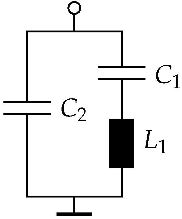
The circuit needs to be expanded with a two pole filter that ensures that for the WPT frequency of 180 kHz, node B (see Figure 2) is set to ground potential, and for the data transmitting frequency, the potential at node B is not influenced by the filter. Figure 3 shows the two pole filter used. This simple circuit has an anti-resonant frequency and a higher resonant frequency. The anti-resonant frequency is the one where the impedance of the filter becomes low in order to ensure the virtual ground potential at node B. In our case this frequency is set at 180 kHz. In order to achieve a high impedance of the filter at the data transmission frequency of approx. 300 kHz, the resonance of the filter needs to be set at this frequency.
In this case, the resonance is calculated from the series connection of the inductance and the two capacitors. The frequency of the anti-resonant pole is calculated from the series connection of the inductance and just the capacitor . The resonant () and anti-resonant () frequencies of the filter are therefore calculated using the following equations:
3.1.1. Frequency Response of the Interlinked Oscillators
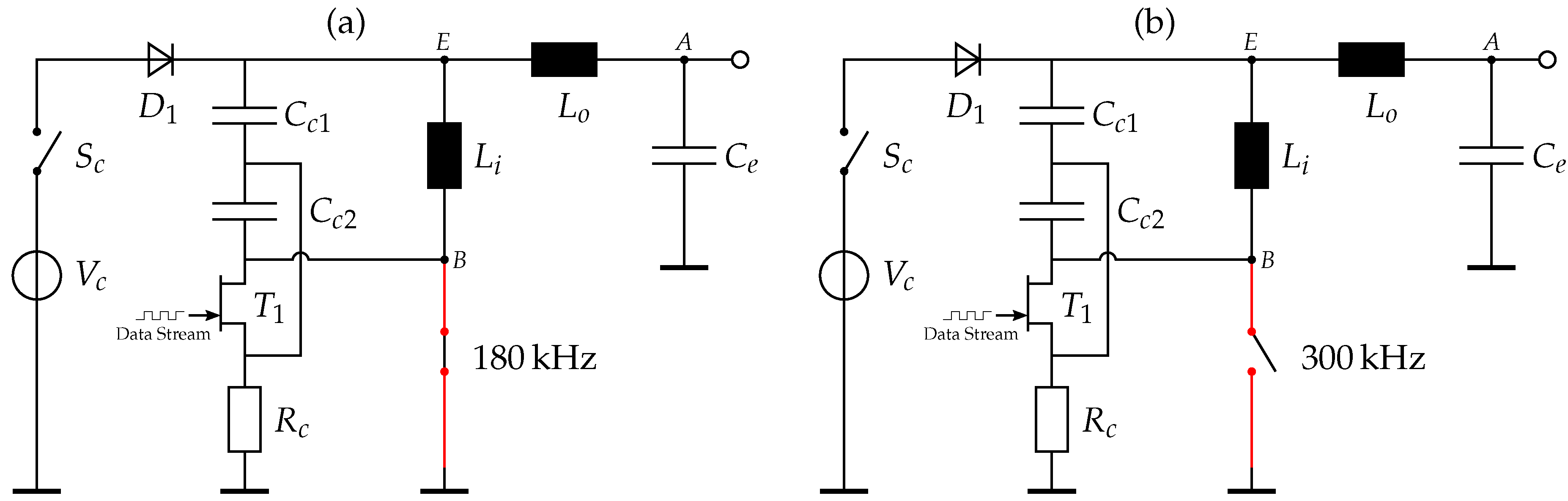
An advantage in dealing with interconnected LC resonant circuits is the fact that at the resonant/anti-resonant frequency of a subsystem, those sub-circuits can be ideally either replaced with a virtual open connection or a virtual short circuit. Since our transmitter needs to deal only with two frequencies, sub-circuits with those two resonant or anti-resonant frequencies can be replaced with one of the named two options. Because of this, the presented two pole filter can be connected to our circuit without any kind of impedance transformer. In the following, Figure 4 shows the equivalent circuit of the two cases where the used filter is replaced with either a short circuit or an open connection. This simplified circuit is valid for ideal components; using real components, the equivalent resistance of the virtual switch in both situations depends on the quality factor of the components. For the simulation presented in Section 4.1, the capacitors are modeled as ideal capacitors and the inductance is modeled, including a series resistance of . For our prototype presented in Section 4.2, the used inductance is chosen regarding a low series resistance, in order to be as close as possible to the ideal case.
In order to resonate at exactly 180 kHz, the interconnection between the tapped WPT LC circuit coil and the Colpitts oscillator capacitors ( and ) must be considered. At the resonant frequency, the amount of the inductive part of the impedance of a circuit must correspond to the amount of its capacitive part. Since the values for the capacitors and and the inductance are given, the capacitance can be calculated for a chosen offset inductance using the following equation (note that the angular frequency is set to ):
with
and the constraint that must be inductive and cannot be zero.
The capacitance in Equation (4) is the series connection of the capacitors and
The Colpitts oscillator is calculated by solving the following equation for the selected component:
In those presented equations, the resistor is not taken into account. By choosing an ohmic value that is high compared to the reactance of the components , and at the used frequency, it does not significantly influence the resonant frequency of the calculated sub-circuit. The interconnection of the Colpitts oscillator and the LC parallel resonant circuit, including the presented two pole filter, is given in Figure 5a. The equivalent circuit for calculating its frequency response is given in Figure 5b. Therefore, the transistor , the power supply of the Colpitts oscillator, the switch , and the diode are omitted. In doing so, the transistor is considered to be switched off, and the same for the voltage source . A separate voltage source connected in series to the inductance is used in the equivalent circuit in Figure 5 in order to take the voltage inducted by the inductive power supply into account. The frequency response of the named equivalent circuit is calculated for two output voltages. Node A defines the output voltage for the WPT oscillator, and node B, the Colpitts oscillator output voltage .
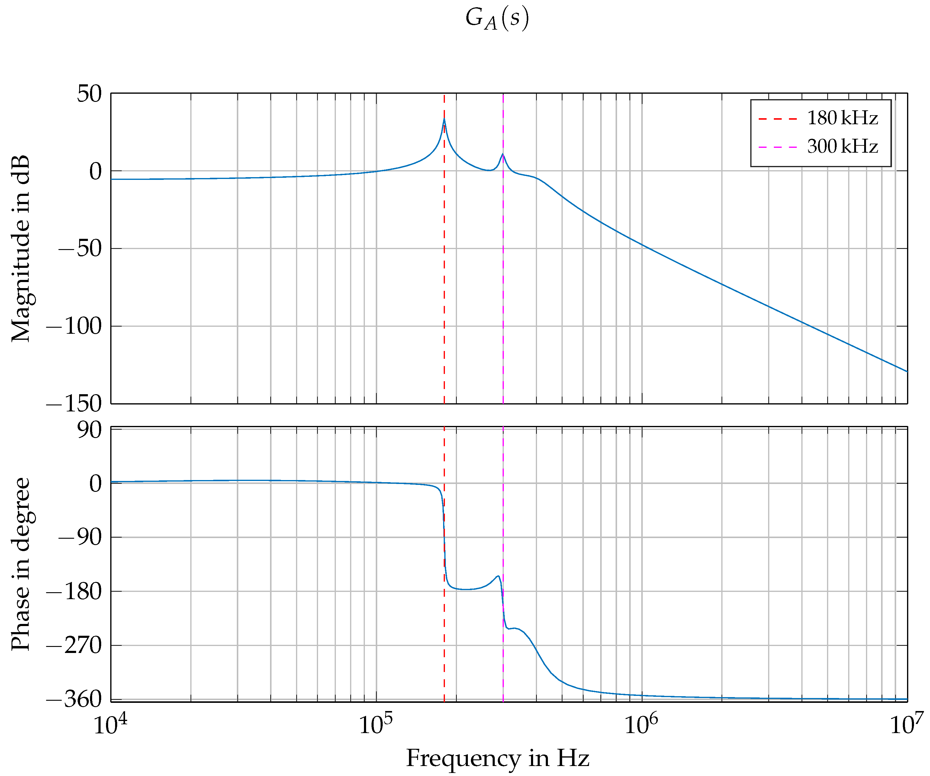
In order to calculate the frequency responses, the transfer functions for the two output voltages need to be calculated. Therefore, the mesh current method is used to define the equation system for the circuit. This is solved using Matlab by MathWorks (2020b, MathWorks, Natick, MA, USA). The voltage source in series to the inductance is therefore used as input voltage. The transfer function for the output voltage is a rational fraction with a seventh-order polynomial in the denominator. Its Bode plot is shown in Figure 6. The main resonance at the frequency of 180 kHz is clearly recognizable. It is clear that the WPT receive circuit with the transfer function has a second resonance at 300 kHz. This second resonance is caused due to the existing connection to the capacitors and . It is therefore important to emphasize that this second resonance is clearly damped by the resistor (which is the resistor at the source pin of the JFET transistor of the Colpitts oscillator amplifier circuit) and is therefore not relevant for the functionality of the energy receive circuit.
In order to design the WPT receive circuit, the voltage at node A will be rectified and used to load a capacitor, and the stored energy is consequently used to power the sensornode electronics, as well as the data transmission circuit. Additionally, for (see Figure 5), the transfer function is calculated and the Bode plot generated. Additionally, the transfer function is a seventh-order transfer function. Its Bode plot is depicted in Figure 7.
At node B, the inductance and the capacitor of the Colpitts oscillator are linked together. It is clearly visible that the resonance frequency at this node corresponds with the chosen data transmission frequency of 300 kHz. It is also obvious that at node B, the WPT frequency of 180 kHz is damped in order to enable the functionality of the Colpitts oscillator. By comparing this with Figure 4, the high damping of the named frequency is equivalent to the virtual connection to the ground depicted in it.
3.1.2. Energy Storage and Provision for the Data Transmission Circuit
In order to implement the energy storage sub-circuit, the alternating voltage at node A (see therefore, Figure 5) needs to be rectified for charging the capacitor that is used to temporarily store the energy. A half-wave rectification is used for this aim. According to [15], this type of rectification is suitable for a voltage input and generates a voltage output. It would not be applicable for a current input, as would be the case if a series resonant oscillator were used as a WPT receive circuit. The negative half-wave of the common current through the whole series connection would be cut off.
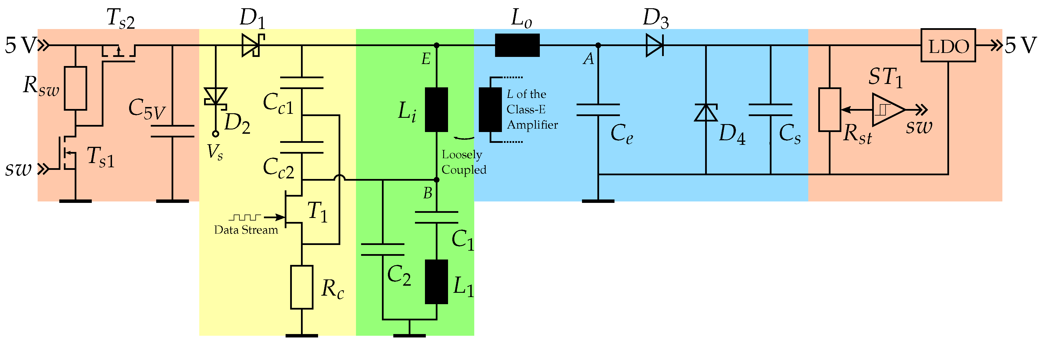
As already mentioned, the transmitter is planned to work according to a two-step procedure. In the first step, a capacitor is loaded with the energy obtained from the WPT LC parallel resonant circuit. As soon as the voltage across this capacitor reaches a defined value, the transmitter switches to the second step and uses the stored energy for powering the sensor and sending back the data. This, until the voltage across the named capacitor reaches a defined low limit where the transmitter switches back to the first step. The switching between those two steps is achieved using a Schmitt trigger that controls the voltage across the capacitor. In order to achieve a constant voltage for powering the sensor and the required operational amplifiers, as well as the Colpitts oscillator, a low dropout voltage regulator (LDO) is used. The output signal of the Schmitt trigger is used to switch a solid state switch realized with two MOSFET transistors. The circuit for this switch was taken from the literature [16]. The advantage of using this simple switch circuit is the fact that it needs no supply voltage, and the switch remains open if no voltage is given at its input and control input. This is crucial in order to enable the powering up of the transmitter. In this case the voltage across the storage capacitor is allowed to be 0 V at the timestamp .
Figure 8 shows the circuit from Figure 5a expanded by the solid state switch (, and ) and the sub-circuit used to store the energy in the capacitor . The Schmitt trigger depicted in Figure 8 as one building block is realized in practice as an operational amplifier-based, non-inverting Schmitt trigger. The resistor in its feedback loop and the one at the positive input of the operational amplifier are summarized using a potentiometer. Additionally, the reference voltage at the negative input of the used operational amplifier is generated from the 5 V LDO output voltage via an adjustable voltage divider. This enables a complete adjustment of the switching thresholds of the Schmitt trigger. As an operational amplifier, a rail-to-rail model is used.
The additional Zener diode depicted in Figure 8 is used to limit the voltage across the capacitor ; its breakdown voltage is of course higher than the high switching level of the Schmitt trigger. Basically, this diode is used as a safety feature in order to limit the voltage across the capacitor if the switch levels of the Schmitt trigger are not set correctly. For the diodes and , we choose to use Shottky diodes due to their lower voltage drop compared to normal diodes.
For our first prototype, we use a digital temperature sensor; this is not depicted in the circuit in Figure 8. Its voltage supply is the pin in Figure 8. The used sensor provides the measured value as a pulse width coded signal, where the temperature can be calculated from the ratio between the high and the low level of the signal. In order to implement the on-off keying of our data transmission, this signal is used for switching the Colpitts oscillator on and off. For the time step 0, at which the capacitor is completely discharged, the transmitter needs to be powered up until the voltage across this capacitor reaches the upper limit set by the Schmitt trigger for getting to the working point where the transmitter toggles between the two described working steps. In order to permit the charging up of the capacitor, the behavior of some components such as the voltage regulator, the operational amplifier, and the transistor switch need to be investigated for low supply voltages. We use a pull down resistor of a few kilo Ohm at the output of the operational amplifier in order to ensure a low signal level at its output during the powering up stage of the transmitter. This is performed in order to ensure an open solid state switch status during this process.
For our investigations and feasibility examinations, the schematic depicted in Figure 8, including the previously described Schmitt trigger, is first simulated and then realized as a prototype. The WPT/data transmitting coil is connected with a cable to the prototype circuit on a printed circuit board. This allows for better handling during the debugging procedure, since only the coil needs to be placed in the inductively powered photoreactor.
4. Results
This chapter deals with the achieved results. First, the circuit is simulated using SPICE software (LTspice by Analog Devices, Wilmington, MA, USA) before the first prototype is built up. As a power supply for the prototype, we use a 150 W laboratory scale inductive power supply conceived for the already named internal illumination system. For the simulations the SPICE circuit of the power supply presented in [10] is used.
4.1. Simulation Results
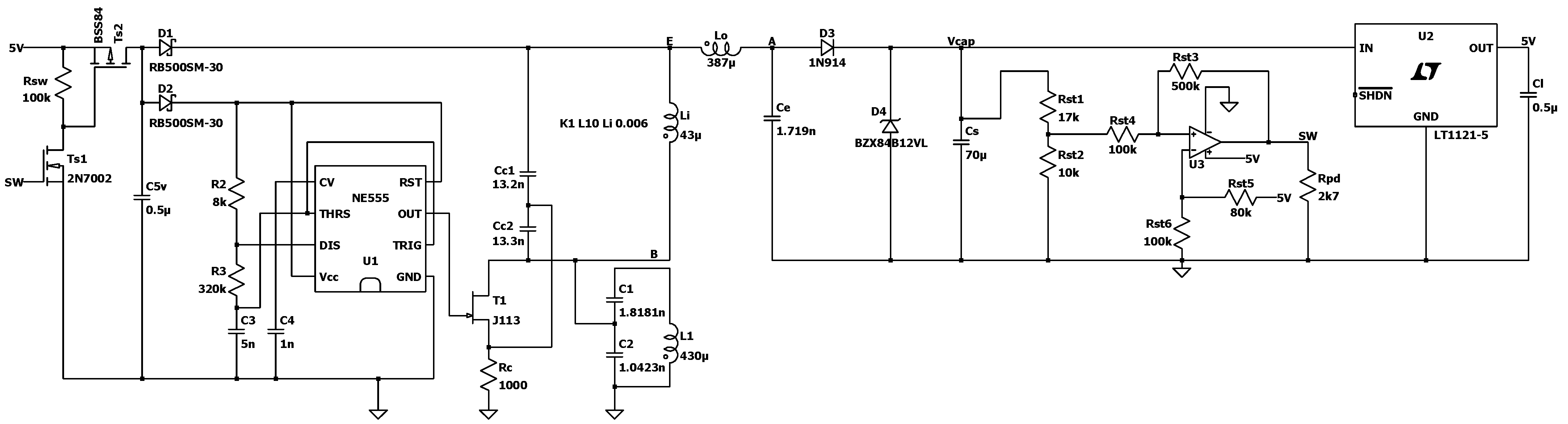
We simulated our transmitter circuit using the class-E based inductive power supply from [10]—Figure 9, but without the multiple receiver part, which is also depicted in this figure.The coupling factor between the class-E amplifier inductance and our transmitter coil is set to . In our case, the coupling factor is difficult to determine, since it changes with changing position of the transmitter inside the reactor. Therefore, the given value is just an estimation. The order of magnitude of the chosen coupling factor was selected based on the values given in [10], taking into account that our coil is bigger compared to the coil used in the wireless light emitters. Whether the order of magnitude of the coupling factor has been chosen correctly can only be checked practically with a prototype in the laboratory.
In order to simulate the data stream of a sensor, a square wave generator based on the NE555 was implemented in our circuit simulation. Its output signal is used to switch the Colpitts oscillator on and off. Figure 9 shows the simulated circuit; the results are given in Figure 10, Figure 11 and Figure 12.
In Figure 10, the voltage is the voltage across the capacitor . This voltage is also the positive envelope of the WPT receive oscillator voltage decreased by the voltage drop of the diode . The two-step operation mode of the transmitter is clearly visible, as well as the powering up stage. As can be seen in Figure 10, the switching levels for the two-step operation are set to approx. 9 V for the upper level and approx. V for the lower level. The transmitter, once powered up, toggles between the two operation steps. The energy receive step, in Figure 10, is the step between approx. 245 ms and 330 ms; and the data transmitting step, in Figure 10 is, e.g., the step between approx. 225 ms and 245 ms or between 330 ms and 350 ms. By knowing the capacity value of , the voltage drop through it during the data transmitting step, and by knowing its duration, the mean value of the power consumption can be calculated for the data transmitting step, resulting in approx. . The same is achieved for the energy receiving step in order to calculate the mean value of the power harvested from the magnetic field of the inductive power supply. This results in approx. . The voltage is the voltage at node B in Figure 9. During the data transmitting step, the on-off switched Colpitts oscillator amplitudes can clearly be seen. A zoomed-in representation of this signal during a data transmitting state of the transmitter is shown in Figure 11. The oscillation frequency of 300 kHz during 200 s of the on-state of the Colpitts oscillator was verified by performing the fast Fourier transformation in the SPICE software environment. The resulted data are plotted in Figure 12.
4.2. Practical Results in the Laboratory
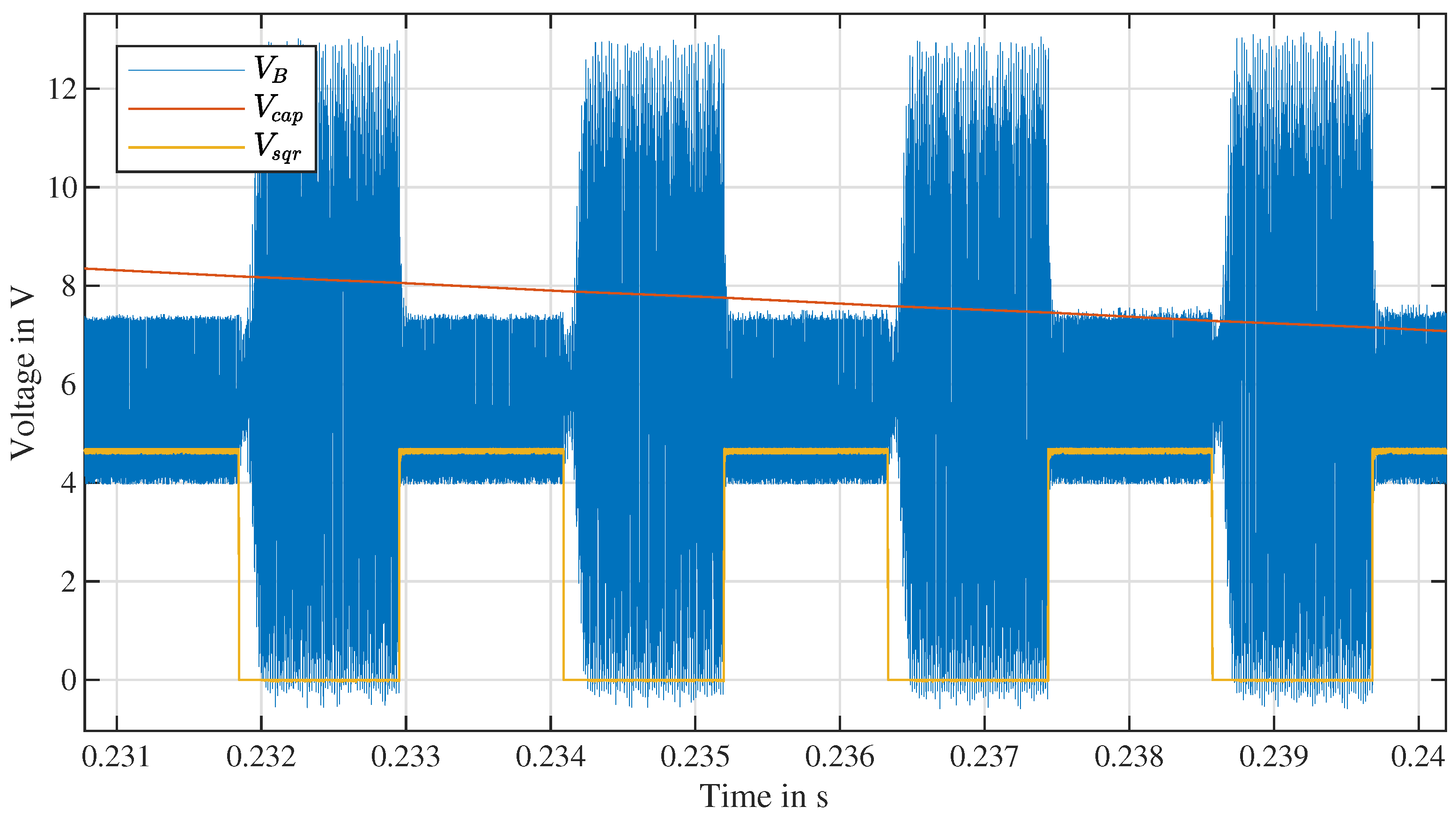
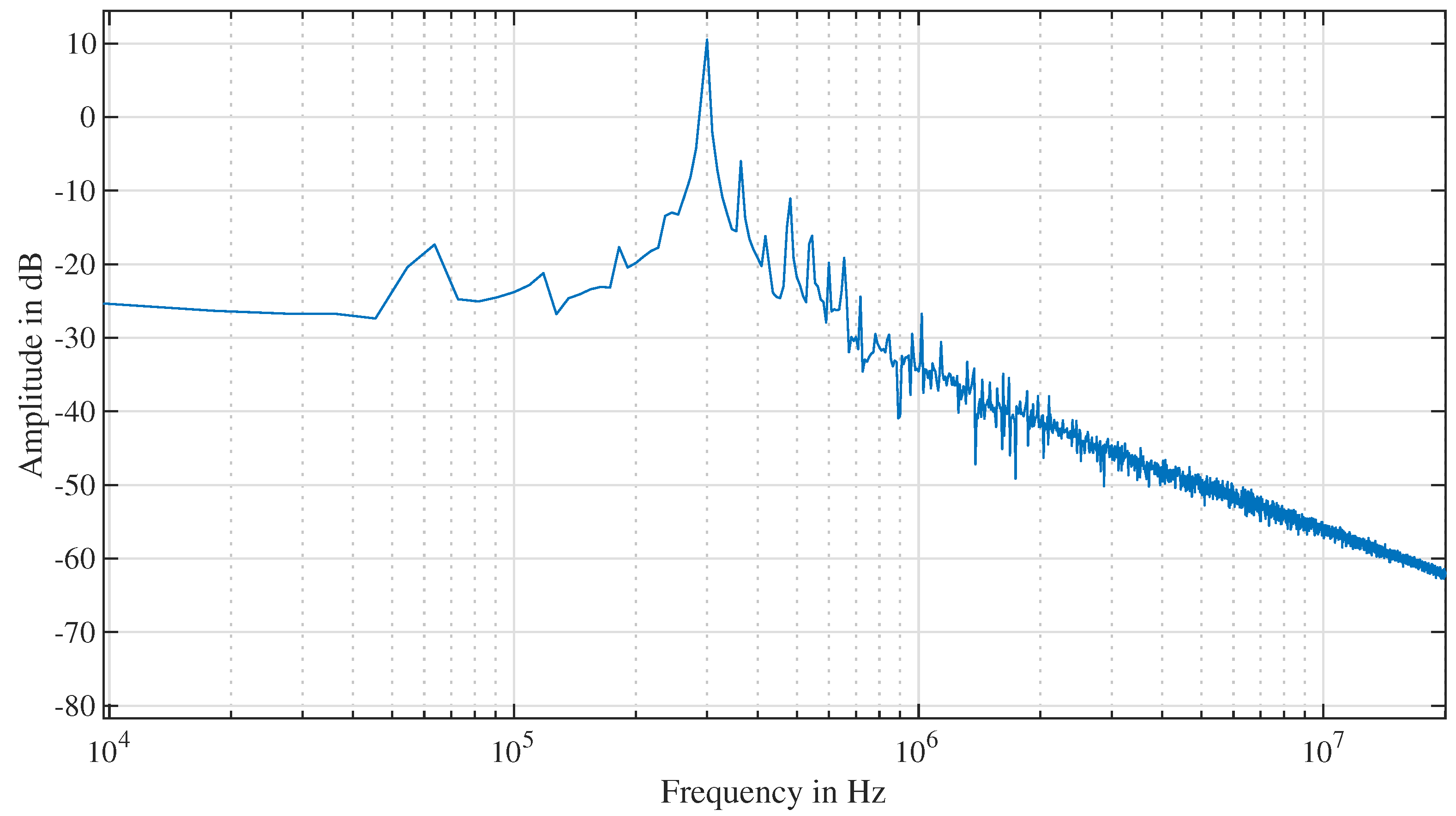
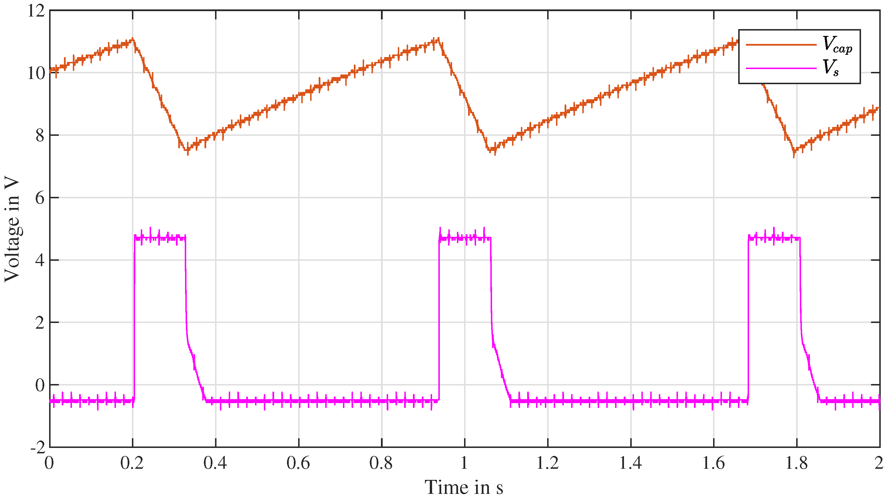
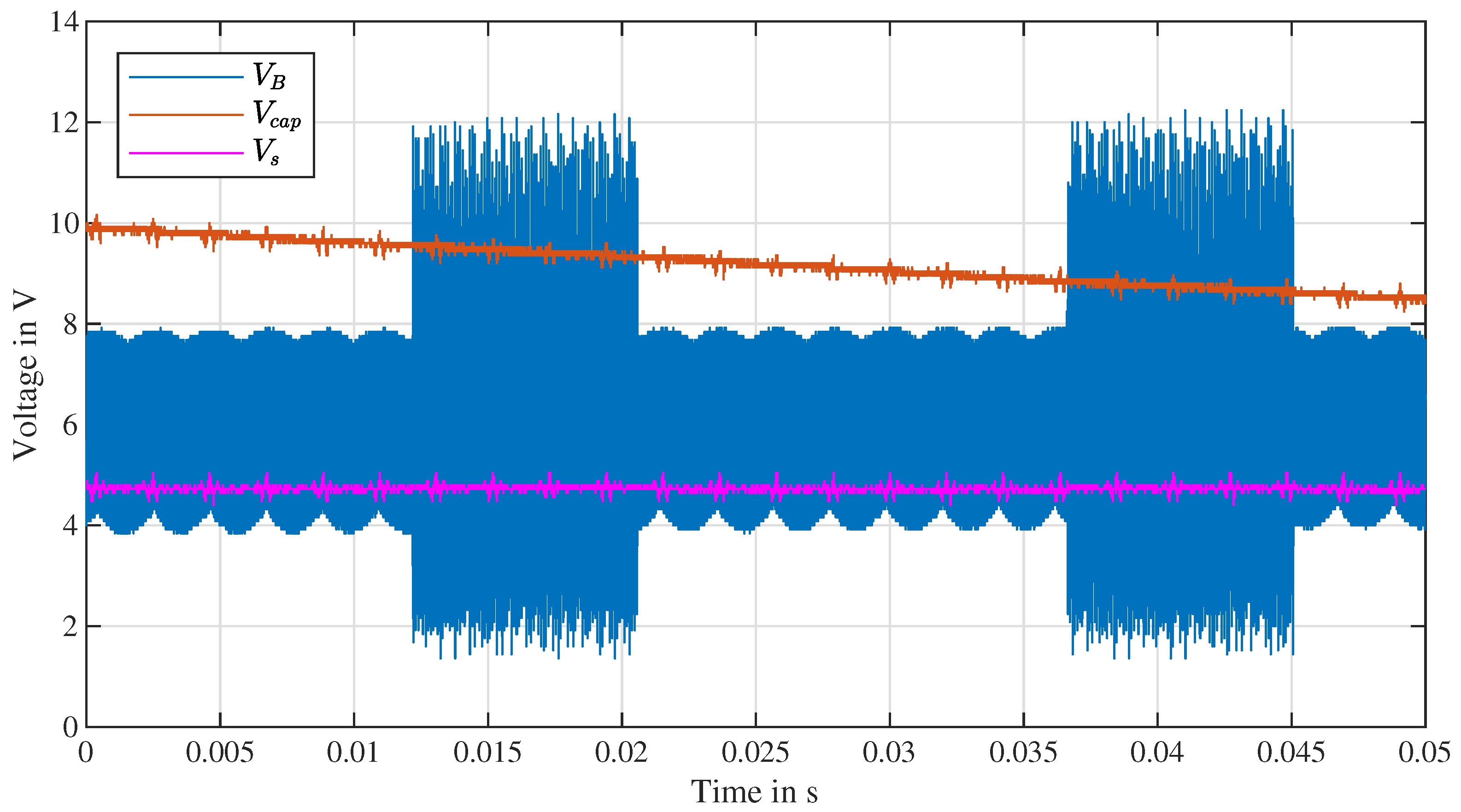
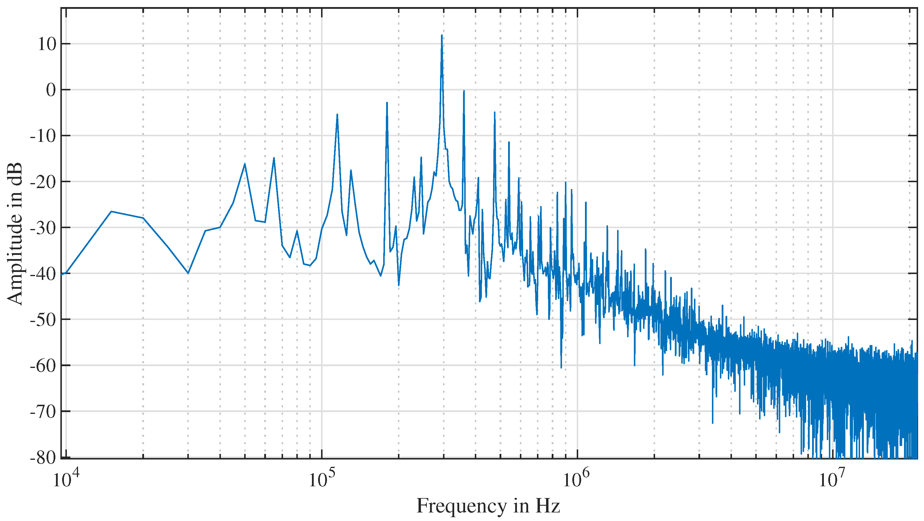
The transmitter is realized on a circuit board. We use a digital temperature sensor that encodes the temperature value as a pulse width coded signal. Since we use the on-off keying, the pulse width coded output signal can be used to switch the Colpitts oscillator. The oscillator behaves inversely to the switching levels of the input signal: for a low level at its JFET transistor gate the oscillator is switched on and vice versa. Therefore, the output signal of the sensor is inverted, and additionally, its low level can be adjusted in order to optimize the amplification of the Colpitts oscillator. This is performed in order to maximize its output amplitudes. The circuit is realized based on the values shown in Figure 9. The energy storing capacitor on our prototype has a much bigger value (820 F) compared to the one used in the simulation, where a lower capacity value was used in order to reduce its charging time, and so, the simulation time. The transistors and and the diodes were replaced with components with similar characteristics on the prototype. Instead of the square wave generator, a real temperature sensor is used, as described above. As for the inductive power supply, a 150 W class-E amplifier, which was developed for the inductively powered wireless internal illumination of photoreactors, is used. Its resonant frequency is 180 kHz. Crucial and important signals measured on our prototype are shown in Figure 13 and Figure 14. The voltage across the capacitor is depicted in orange. Clearly recognizable in Figure 13 are the switching limits set by the Schmitt trigger, where the high switching limit is set to approx. 11 V and the low level at approx. V. The signal depicted in magenta is the signal which in Figure 8 is named as which is basically the supply voltage for the sensor. As with the simulation, we also calculated the mean power values for the two operating steps for our prototype. The mean power consumption during the data transmitting step results in approx. , and the mean power harvested from the magnetic field during the energy receiving step results in approx. . Figure 14 shows the on-off coded data bits of the temperature sensor. We performed the fast Fourier transformation of the signal at node B during 200 s of the on state of the Colpitts oscillator in order to prove the transmitting frequency. Figure 15 shows its result. The main frequency is clearly the resonance frequency at approx. 300 kHz. Using real components can influence the behavior of a circuit when compared to a simulation result. This is clearly recognizable in Figure 15. The frequency of the inductive power transmission is not completely filtered out in using the two pole filter from the Section 3 build with real components. The Fourier transformation reveals peaks at the power supply frequency of 180 kHz and at its first harmonic (360 kHz). Since the amplitudes of those peaks are more than 12 dB lower compared to the main oscillation frequency, it is not a big deal for our purpose.
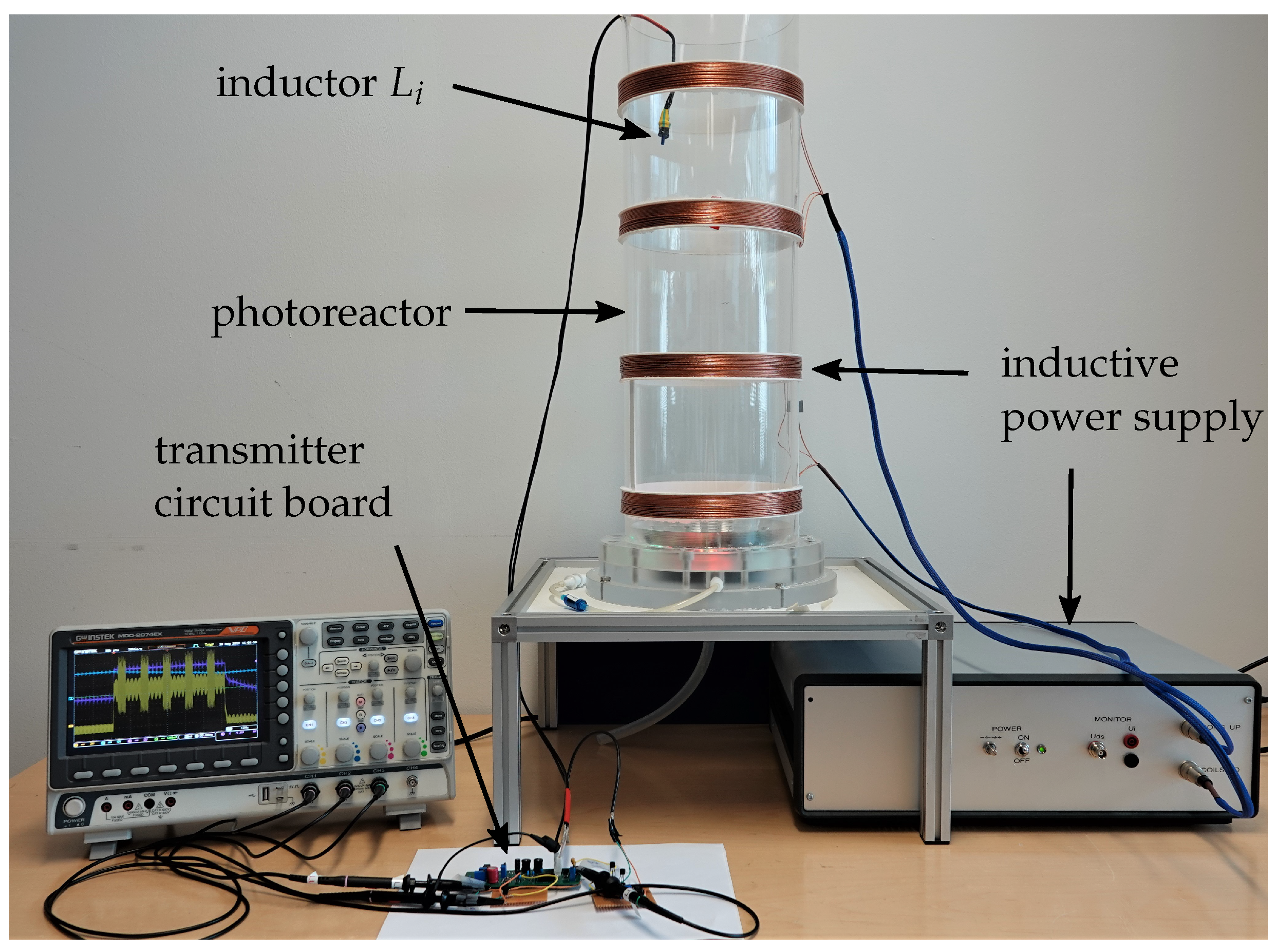
Since our prototype is not miniaturized, its functionality was tested with only the WPT/data transmitting coil placed in the magnetic field inside the reactor. Therefore, the named coil was connected with cables to the circuit board of our transmitter prototype, which was placed outside the reactor. This allowed us a better handling during the debugging phase of building up this first prototype, since all signal measurements on the circuit board could be performed outside the photoreactor. The setup can be seen in Figure 16. On the left side in Figure 16, the oscilloscope with the measured signals can be seen. In yellow, the on-off coded data bits at the Colpitts oscillator (node B) are clearly recognizable. This signal corresponds to the voltage plotted in Figure 14. At the outer diameter of the photoreactor, the four coils of the inductive power supply can be seen.
5. Discussion
The achieved results underpin the functionality of the developed transmitter circuit, where the interconnection of a LC parallel resonant oscillator and a Colpitts oscillator represents the centerpiece of it. If the simulation results are compared with the measurements performed on the prototype, the much longer charging time of the prototype’s storage capacitor can be noticed. This fact has two main reasons: the first one is the fact that the storage capacitor value on the prototype is much bigger compared to the one used in the simulation, and the second reason is that the high switching level was set at a higher voltage for the prototype. We performed the simulations with a lower switching level and a smaller storage capacitor value in order to reduce the simulation time. The circuit simulation was performed in order to prove the feasibility before building up the prototype. We tested the functionality of the transmitter architecture using our prototype, where only the WPT/data transmitting coil was placed in the magnetic field inside the reactor. The mean power consumption level during the data transmitting step is much higher for the prototype compared to the simulation. The reason for this difference lies probably in the simpler simulated circuit, where no real sensor and its additional electronics are simulated. Additionally due to the higher switching levels of the Schmitt trigger on our prototype, more power is dissipated in the voltage regulator, which also results in a higher power consumption. The mean value of the harvested power of our transmitter is approx. twice the value of the simulation. This shows that for the simulation, we chose a somewhat low coupling factor between the transmitter and the inductive power supply.
The next two main steps are the miniaturization of the sensornode itself on the one hand, and the expansion of the system, in order to use more than one sensornode, on the other hand. In order to enable the miniaturization of our sensornode, the whole circuit needs to be realized on a small printed circuit board, which can be placed like the wireless light emitters from [9] inside a plastic sphere. The size of the sphere we are aiming for is in the range of 2 to 3 cm in diameter. We chose a circuit architecture where we just needed one coil in order to receive energy and to transmit the data. The transmitter coil, which acts as antenna, will be one of the biggest components of our circuit, since it cannot be realized as a miniaturized component. Therefore, in having just one transmitter coil, the amount of space needed is reduced, which is a clear advantage for the miniaturization.
For operating more than one sensornode, a method needs to be adopted in order to coordinate the data transmission of more transmitters. This could be performed using different data transmitting frequencies in order to distinguish between the transmitted data of multiple sensornodes. A drawback of this method could be the receiver architecture, they would therefore need to be designed for receiving data at different frequencies. Another method could be some kind of time synchronization between the sensornodes in order to coordinate the data transmission. This is difficult to realize, since the here presented architecture is designed to just transmit data, and not for receiving data. Moreover, the additional electronics would need space on the circuit board and energy for being powered, which for our passive architecture is limited. These aspects clearly need additional research. For now, the variant of using different transmitting frequencies seems the most suitable.
For the here presented study, the measurements and tests were performed with one single sensornode. The receivers presented in [14], which were used to perform the localization of a transmitting coil in air and in absence of the inductive power supply, need to be adopted for their use in the here presented setup. The near inductive power supply would induct voltages in the receiver coils that would be higher than the rail voltages of the operational amplifiers used. The received signals would be distorted, since the receiver coils are directly connected to the input of an operational amplifier. We already performed simulations and some first practical tests of a modification of the receiver circuit presented in [14], in order to counteract this problem. For damping the signals inducted at the frequency of the power supply, a passive filter is needed where no operational amplifiers are used. We solved this problem (for a setup with one single sensornode—one single data transmitting frequency) in connecting the receiver coil in series with a capacitor, resulting in a series resonant circuit. This in turn is connected in parallel with a second series LC circuit. The resulting LCLC network is tuned in order to conduct the voltages at 180 kHz to ground and to resonate at the node between the two LC series circuits at the data transmitting frequency (in this case, 300 kHz). The voltage at this node is the output of this network. It is additionally filtered and amplified with the series connection of two of the receiver circuits which were used in [14], resulting in an eighth-order active bandpassfilter. This receiver setup was tested with just one single receiver coil. Therefore, the next step in the receiver adaptation is to test this setup with the orthogonal coils used in [14].
6. Conclusions
The circuit design of an inductively powered transmitter based on the interconnection af a Colpitts and a parallel resonant LC oscillator is discussed in this paper. Both oscillators share the same inductance, which is used as an antenna for sending inductively the measured data, and for receiving the energy supplied by an inductive power supply. The used frequencies are in the low frequency range: the inductive power supply works at a resonant frequency of 180 kHz and the measured data is transmitted at 300 kHz. The presented circuit is introduced starting from its centerpiece, which is the named interconnection of the two oscillators; this is consequentially extended by all the additional electronics required. Moreover, the frequency behavior is analyzed using Bode plots of two crucial transfer functions of this transmitter: the frequency behavior for the data sending circuit node, as well as the one for the energy receiving sub-circuit. Its functionality is demonstrated using SPICE simulations, as well as practically, by building a prototype and measuring crucial signals on it.
Author Contributions
Conceptualization, D.D. and A.S.; methodology, D.D. and A.S.; validation, D.D.; writing—original draft preparation, D.D.; writing—review and editing, D.D. and A.S.; visualization, D.D.; supervision, A.S.; project administration, A.S.; funding acquisition, D.D. All authors have read and agreed to the published version of the manuscript.
Funding
This research was funded by the Tyrolean Science Fund (TWF, Project No. 18689).
Conflicts of Interest
The authors declare no conflict of interest.
Abbreviations
The following abbreviations are used in this manuscript:
| WPT | Wireless Power Transfer |
| WLE | Wireless Light Emitter |
References
- Hott, M.; Hoeher, P.A.; Reinecke, S.F. Magnetic Communication Using High-Sensitivity Magnetic Field Detectors. Sensors 2019, 19, 3415. [Google Scholar] [CrossRef] [PubMed]
- Wu, J.; Zhao, C.; Lin, Z.; Du, J.; Hu, Y.; He, X. Wireless Power and Data Transfer via a Common Inductive Link Using Frequency Division Multiplexing. IEEE Trans. Ind. Electron. 2015, 62, 7810–7820. [Google Scholar] [CrossRef]
- Xie, L.; Shi, Y.; Hou, Y.T.; Lou, A. Wireless power transfer and applications to sensor networks. IEEE Wirel. Commun. 2013, 20, 140–145. [Google Scholar] [CrossRef]
- Yang, Y.; El Baghdadi, M.; Lan, Y.; Benomar, Y.; Van Mierlo, J.; Hegazy, O. Design Methodology, Modeling, and Comparative Study of Wireless Power Transfer Systems for Electric Vehicles. Energies 2018, 11, 1716. [Google Scholar] [CrossRef]
- Shadid, R.; Noghanian, S. A literature survey on wireless power transfer for biomedical devices. Int. J. Antennas Propag. 2018, 2018, 4382841. [Google Scholar] [CrossRef]
- Zhou, Y.; Liu, C.; Huang, Y. Wireless Power Transfer for Implanted Medical Application: A Review. Energies 2020, 13, 2837. [Google Scholar] [CrossRef]
- Bouattour, G.; Elhawy, M.; Naifar, S.; Viehweger, C.; Ben Jmaa Derbel, H.; Kanoun, O. Multiplexed Supply of a MISO Wireless Power Transfer System for Battery-Free Wireless Sensors. Energies 2020, 13, 1244. [Google Scholar] [CrossRef]
- Kanoun, O.; Khriji, S.; Naifar, S.; Bradai, S.; Bouattour, G.; Bouhamed, A.; El Houssaini, D.; Viehweger, C. Prospects of Wireless Energy-Aware Sensors for Smart Factories in the Industry 4.0 Era. Electronics 2021, 10, 2929. [Google Scholar] [CrossRef]
- Heining, M.; Sutor, A.; Stute, S.; Lindenberger, C.; Buchholz, R. Internal illumination of photobioreactors via wireless light emitters: A proof of concept. J. Appl. Phycol. 2015, 27, 59–66. [Google Scholar] [CrossRef]
- Sutor, A.; Heining, M.; Buchholz, R. A Class-E Amplifier for a Loosely Coupled Inductive Power Transfer System with Multiple Receivers. Energies 2019, 12, 1165. [Google Scholar] [CrossRef] [Green Version]
- Burek, B.O.; Sutor, A.; Bahnemann, D.W.; Bloh, J.Z. Completely integrated wirelessly-powered photocatalyst-coated spheres as a novel means to perform heterogeneous photocatalytic reactions. Catal. Sci. Technol. 2017, 7, 4977–4983. [Google Scholar] [CrossRef]
- Lauterbach, T.; Lüke, T.; Büker, M.J.; Hedayat, C.; Gernandt, T.; Moll, R.; Grösel, M.; Lenk, S.; Seidel, F.; Brunner, D.; et al. Measurements on the fly—Introducing mobile micro-sensors for biotechnological applications. Sens. Actuators A Phys. 2019, 287, 29–38. [Google Scholar] [CrossRef]
- Groben, D.; Thongpull, K.; Kammara, A.; König, A. Neural Virtual Sensors for Adaptive Magnetic Localization of Autonomous Dataloggers. Adv. Artif. Neural Syst. 2014, 2014, 394038. [Google Scholar] [CrossRef]
- Demetz, D.; Sutor, A. Inductive Tracking Methodology for Wireless Sensors in Photoreactors. Sensors 2021, 21, 4201. [Google Scholar] [CrossRef] [PubMed]
- Van Schuylenbergh, K.; Puers, R. Inductive Powering: Basic Theory and Application to Biomedical Systems; Analog Circuits and Signal Processing; Springer: Dordrecht, The Netherlands, 2010. [Google Scholar]
- Horowitz, P.; Hill, W. The Art of Electronics; Cambridge University Press: Cambridge, UK, 1989. [Google Scholar]
Figure 1.
Conceptualization of an internal illuminated photoreactor expanded by a wireless sensor system.
Figure 1.
Conceptualization of an internal illuminated photoreactor expanded by a wireless sensor system.

Figure 2.
Interconnected oscillators: the yellow marked components correspond to the data transmitting sub-circuit; the blue marked ones to the energy receive sub-circuit, and the green ones are the shared components for both sub-circuits.
Figure 2.
Interconnected oscillators: the yellow marked components correspond to the data transmitting sub-circuit; the blue marked ones to the energy receive sub-circuit, and the green ones are the shared components for both sub-circuits.

Figure 3.
Resonant/anti-resonant LC filter.

Figure 4.
Interconnected oscillators—equivalent circuits for the filter at 180 kHz (a) and 300 kHz (b).
Figure 4.
Interconnected oscillators—equivalent circuits for the filter at 180 kHz (a) and 300 kHz (b).

Figure 5.
Interconnected oscillators (a) and the simplified equivalent circuit used for calculating the transfer functions (b).
Figure 5.
Interconnected oscillators (a) and the simplified equivalent circuit used for calculating the transfer functions (b).

Figure 6.
Bode plot of the transfer function .

Figure 7.
Bode plot of the transfer function .

Figure 8.
Transmitter electronics; the voltage at pin is used to supply the sensor with energy. The yellow marked circuit part corresponds to the data transmission sub-circuit, the blue marked one to the energy receiving sub-circuit, and the green marked components are the shared components for both these sub-circuits. The red marked circuit part is used for switching between the two operational steps and for supplying the needed for the components like the sensor, the Schmitt trigger etc.

Figure 9.
Simulated transmitter circuit inductively coupled to the class-E amplifier circuit from [10], which is not depicted in this picture.
Figure 9.
Simulated transmitter circuit inductively coupled to the class-E amplifier circuit from [10], which is not depicted in this picture.

Figure 10.
Simulated voltages across the capacitor () and at node B () from the transmitter circuit in Figure 9.
Figure 10.
Simulated voltages across the capacitor () and at node B () from the transmitter circuit in Figure 9.

Figure 11.
Simulated voltages across the capacitor (), at node B (), and the signal at the gate of the JFET transistor () from the transmitter circuit in Figure 9. The Colpitts oscillator reacts inversely to the switching level at its transistor.
Figure 11.
Simulated voltages across the capacitor (), at node B (), and the signal at the gate of the JFET transistor () from the transmitter circuit in Figure 9. The Colpitts oscillator reacts inversely to the switching level at its transistor.

Figure 12.
Fast Fourier transformation of the signal at node B () during 200 s of the on-state of the Colpitts oscillator generated from the simulated data.
Figure 12.
Fast Fourier transformation of the signal at node B () during 200 s of the on-state of the Colpitts oscillator generated from the simulated data.

Figure 13.
Voltages across the capacitor () and the signal measured on our prototype.

Figure 14.
Voltages across the capacitor (), at node B () and the signal measured on our prototype.

Figure 15.
Fast Fourier transformation of the signal at node B () during 200 s of the on-state of the Colpitts oscillator measured on our prototype.
Figure 15.
Fast Fourier transformation of the signal at node B () during 200 s of the on-state of the Colpitts oscillator measured on our prototype.

Figure 16.
Laboratory setup where only the WPT/data transmitting coil is placed inside the photoreactor. The circuit board with the remaining components is placed in front of the reactor. On the left side, the oscilloscope depicts the measured signals.
Figure 16.
Laboratory setup where only the WPT/data transmitting coil is placed inside the photoreactor. The circuit board with the remaining components is placed in front of the reactor. On the left side, the oscilloscope depicts the measured signals.

Publisher’s Note: MDPI stays neutral with regard to jurisdictional claims in published maps and institutional affiliations. |
© 2022 by the authors. Licensee MDPI, Basel, Switzerland. This article is an open access article distributed under the terms and conditions of the Creative Commons Attribution (CC BY) license (https://creativecommons.org/licenses/by/4.0/).
Share and Cite
MDPI and ACS Style
Demetz, D.; Sutor, A. Inductively Powered Sensornode Transmitter Based on the Interconnection of a Colpitts and a Parallel Resonant LC Oscillator. Energies 2022, 15, 6198. https://0-doi-org.brum.beds.ac.uk/10.3390/en15176198
AMA Style
Demetz D, Sutor A. Inductively Powered Sensornode Transmitter Based on the Interconnection of a Colpitts and a Parallel Resonant LC Oscillator. Energies. 2022; 15(17):6198. https://0-doi-org.brum.beds.ac.uk/10.3390/en15176198
Chicago/Turabian StyleDemetz, David, and Alexander Sutor. 2022. "Inductively Powered Sensornode Transmitter Based on the Interconnection of a Colpitts and a Parallel Resonant LC Oscillator" Energies 15, no. 17: 6198. https://0-doi-org.brum.beds.ac.uk/10.3390/en15176198
Note that from the first issue of 2016, this journal uses article numbers instead of page numbers. See further details here.