Article

Optimizing the Spatial Nonuniformity of Irradiance in a Large-Area LED Solar Simulator

Centre for Organic Electronics, University of Newcastle, Newcastle 2308, Australia
*
Authors to whom correspondence should be addressed.
Submission received: 9 October 2022 / Revised: 1 November 2022 / Accepted: 4 November 2022 / Published: 10 November 2022
(This article belongs to the Special Issue Solar Energy: Resources, Technologies and Challenges)

Abstract

:
The solar simulator has allowed all photovoltaic devices to be developed and tested under laboratory conditions. Filtered xenon arc lamps were the gold-standard source for solar simulation of small-area silicon photovoltaic devices; however, scaling these devices to illuminate large areas is neither efficient nor practical. Large-area solar simulation to meet appropriate spectral content and spatial nonuniformity of irradiance (SNI) standards has traditionally been difficult and expensive to achieve, partly due to the light sources employed. LED-based solar simulation allows a better electrical efficiency and uniformity of irradiance while meeting spectral intensity requirements with better form factors. This work details the design based on optical modeling of a scalable, large-area, LED-based, solar simulator meeting Class AAA performance standards formed for inline testing of printed solar cells. The modular design approach employed enables the illuminated area to be expanded in quanta of ~260 cm2 to any preferred illumination area. A 640 cm2 area illuminated by two adjacent PCB units has a measured total emission of 100 mW/cm2, with a SNI of 1.7% and an excellent approximation to the AM1.5G spectrum over the wavelength range of 350–1100 nm. The measured long-term temporal instability of irradiance (TIE) is <0.5% for a 550-min continuous run. This work identifies the design steps and details the development and measurement of a scalable large-area LED-based solar simulator of interest to the PV testing community, and others using solar simulators.

Graphical Abstract

1. Introduction

Advanced testing of photoresponsive materials and photo-affected organisms and substances, including photocatalysis, in a laboratory setting has seen the development of solar simulators [1] as useful tools within materials engineering, biotechnology, and energy science to assess the performance of solar cells and photovoltaic (PV) modules, for medical or cosmetic research, material weathering and lifetime degradation testing for coatings, agricultural lighting systems, and animal husbandry experiments [2,3,4]. There are three standards for characterizing solar simulation: the International Electrotechnical Commission (IEC), IEC 60904-9:2020 [5]; the American Society for Testing and Materials ASTM E-927-19 [6]; the Japanese Industrial Standard JIS C 8912:1998/AMENDMENT 2:2011 [7].
The light sources utilized encompass: xenon and metal halide arc lamps, quartz tungsten filament lamps, and light-emitting diodes (LEDs) where the selection of the emission source can depend on the desired solar simulation application [8]. Table 1 provides an overview of the benefits and drawbacks of each light source implemented in solar simulation. Many different types of solar simulators meeting one or more standards have been designed, developed, and used since the 1960s [9]. Notably, high-pressure xenon gas discharge lamps provide the closest spectral match (SM) to the solar spectral output available from any artificial source; however, these lamps deliver small uniform irradiance fields due the challenge of optically imaging an electrical arc evenly over the test surface.
Rapid advances in high-power light-emitting diodes (LEDs) have provided the opportunity to design and construct solar simulators from arrays of discrete LED light sources. These have been used to precisely imitate the spectral distribution of sunlight through many narrow-bandwidth emitters, as well as match the temporal diurnal intensity variation through advanced current control [10], something not possible with conventional lamp-based solar simulator technology. In addition, with non-silicon photovoltaic cells emerging, a better match between LED emission wavelengths and device absorption has been reported in the literature [11]. These aspects attracted attention as the specific solar simulation requirement supporting roll-to-roll printed organic solar cell development is to have very uniform irradiance across all spectral components over a large area. In device research and development, the cells under test are frequently <5 mm2 in area, meaning that a lower value of SNI, more stringent than the standard norms, is essential [5,6,7]. For discrete LED-emitter-based solar simulator modeling, this requirement for the homogeneity of spectral irradiance remains a challenge [12].
The first reports of LED-based solar simulators were published in the early 2000s, with initial systems limited by the low power output of the LED technology available [13] and the variation in irradiance homogeneity over the illuminated area. In 2006, an array consisting of blue, red, and IR high-brightness LEDs was used to synthesize an irradiance spectrum between 400 and 1100 nm, and Class A+ SNI was achieved [14]. In 2009, the first LED simulator with 100 mW/cm2 of intensity was introduced [15,16], soon followed, in 2011, by a Class AAA-rated design featuring 22 different LED wavelengths that combined to produce a spectral distribution matching AM1.5G from 350 to 1100 nm [17,18]. A scalable large-area solar simulator using 60 different high-power LEDs combining single- and multi-color emission yielding a Class C SNI over the wavelength range of 400–1100 nm was demonstrated [19], where the source plane connected to a long, tapered, mixing light guide creating uniform irradiance at the sample test plane area. The system could be operated in continuous and pulsed modes; however, the system was very large and too difficult to scale up for industrial applications. In 2014, “spike-free” spectral irradiance over the AM1.5 reference spectrum from 23 different LED colors was demonstrated [8]. The LED array was a modular unit comprising 100 LEDs with reflecting side mirrors that can be replicated and arranged to create a larger illumination area. The spectral distribution and SNI were Class A according to ASTM/IEC specifications. The research work into multi-wavelength and multiple light source solar simulators, which are aimed at developing a more accurate and uniform spectral irradiance output over large illumination areas, continues [20,21,22,23,24,25,26,27,28,29].
The work presented here describes the design geometry of a ten-LED color solar simulator, incorporating tessellated hexagonal array geometry, to allow the assembly of a large-area solar simulator (LASS) unit providing a highly uniform illumination area. The prototype was designed, optically modeled, constructed, and evaluated for suitability as a solar simulator under three criteria: SM, SNI for each color of LED, and TIE. A comparison with a xenon-lamp-based solar simulator was performed by measuring the current–voltage response of a variety of solar cells. The results demonstrate that the new LED-based solar simulator design meets the Class AAA classification according to the three official bodies regulating solar simulator standards.

2. Choice of LED and Geometric Location

This section explains the reasoning and approach toward the chosen LED configuration for each modular unit of the LED solar simulator. Each 30 cm × 8.7 cm printed circuit board (PCB) supported 266 LEDs of 10 individual colors and formed the unit building block of the simulator. The PCBs may be aligned in parallel for larger illumination areas in increments of 261 cm2 and were formed from tessellated hexagonal arrangements of 71 LEDs arranged to cover an area of ~65 cm2, as explained below.

2.1. LED Light Sources

The selection of LEDs for the LASS was based on two considerations. First, only high-flux-density LEDs were considered in order to achieve a design irradiance level of 200 mW/cm2, twice the one-Sun-irradiance value specified [5,6,7], thus enabling a greater flexibility in light intensity adjustment and in the spatial geometry of the LEDs in the source plane. Optically, the discrete LED emission from each source color has to be combined to give a uniform distribution per color over the test plane area, and the combination of all. This is achieved, primarily, with distance from the source plane. Light shaping diffusers were used for further uniformity.
Secondly, ten individual diodes were selected to cover the 350–1100 nm wavelength range and the six wavelength intervals defined within the solar simulator standards [5]. The addition of two UV LEDs enhanced 350–400 nm UV emission to allow organic solar cell photovoltaic reliability testing [30,31]. Figure 1a shows the spectral irradiance of the 10 individual LED types and Figure 1b details the ASTM G173-03 hemispherical spectral irradiance of the Sun on a 37° tilted surface (AM1.5G) [32] set against the synthetic spectral irradiance of the modular LED LASS.

2.2. LED Array Configurations

The LEDs were arranged in hexagonal array units to ensure the best flux homogeneity from the minimum number of emitters for each individual color [27]. Hexagonal module geometry aids tessellation and the ten individual LED colors can be configured inside the hexagon cell area with different individual arrangements to provide highly efficient uniform illumination [12,33]. There are many possible configurations for the 71 LEDs of 10 individual colors and each configuration will have a different overall power, uniformity, and thermal constraints [34]. The area of one hexagon unit was chosen small enough (~65 cm2) to allow the LED light intensity to be adjusted with minimum electrical power consumption.
The characteristics and the number (#) of LEDs used in one hexagonal unit of 50 mm side length are listed in Table 2. The optimized layout of the 10 assorted color LEDs is shown in Figure 2a,b. The configuration of LEDs in a hexagonal unit cell was optically modeled in TracePro® software (Lambda Research Corp.) and optimized for irradiance, uniformity, and spectral content. The number of LEDs and the corresponding arrangement for each individual LED light source inside the hexagonal unit cell are shown in Figure 2c.
These hexagonal unit cells can be tessellated, and a rectangular PCB was selected from the combined area as shown in Figure 3. The PCB of 30 cm × 8.7 cm was carefully extracted from the optical model so that replication of this pattern in adjacent PCBs reproduced, seamlessly, the same individual LED color density and, when reflecting surfaces were placed along the edges, reflected the pattern to form a scalable LED LASS unit. An efficient, compact, solar simulator system may be constructed from multiple units of the 261 cm2 area PCBs. The optical modeling of the integrated output of two adjacent boards incorporating 532 LEDs follows in the next section.

3. Optical Raytracing and Modelling

Optical raytracing with TracePro® was also used to evaluate the optical performance of the LED LASS modular arrangement. The optical structure can be separated into the LED source plane (SP) array and shaping components of the mirrored light housing and diffuser, as illustrated in Figure 4a, prior to the sample test plane (STP). The LED SP was simulated as a white painted surface, upon which the LEDs were mounted, while the STP was simulated as a perfect absorber.
In a typical ray optical tracing model, a large number of rays result in a higher precision at the expense of a longer calculation time. A test of the sensitivity of the optical model to the number of rays used was performed, helping to define the minimum number of rays required and a sensible maximum.
One color of LED emission was simulated with seven different ray numbers per individual LED (1 k, 5 k, 10 k, 50 k, 100 k, 500 k, and 1 M rays); then, the intensity distribution was examined at the STP where the STP was placed at 120 mm from the LED SP. The STP intensity distribution maps and the flux intensity for different ray numbers are depicted in Figure 5, showing that the intensity distribution for the 100 k, 500 k, and 1 M ray results were approximately the same with a uniform central region, Figure 5a. The detailed flux intensity and nonuniformity changes within the central region for each ray number are shown in Figure 5b. There was only a 1.48 ± 0.02% change within the central region irradiance uniformity when the ray numbers increased from 100 k to 1 M rays and the raytracing time increased from 4 s to 23 s, respectively, for a single LED. As such, 100 k rays per individual LED were used for simulation in all LED LASS unit design considerations.
The variation in SNI for the reflective housing unit as a function of source-STP distance is shown in Figure 6a. At a distance of 40 mm, a SNI ≤ 10% matching Class C uniformity was obtained. As the LED source-sample distance was increased through the range of 40–100 mm, a SNI ≤ 5% matching Class B uniformity was obtained, whereas for LED source-sample distances of more than 100 mm, Class A performance reflecting a ≤2% deviation in SNI was achieved.
During the ray-tracing analysis, the emitted rays from the LED were optically configured to mimic the properties of the actual LED color. The integrated rays emitted from the SP can reach the STP directly or by reflection, some of the rays may be reflected to the SP, and a small number will possibly scatter in any direction, as shown in Figure 4b.
Rays may be reflected one or multiple times before reaching the STP, which was 20 mm from the measurement surface. A total of 53.2 M rays from the 532 individual LEDs on the PCBs were traced within TracePro®, to simulate the system in a variety of configurations: the bare PCBs; with a poorly reflective light housing; with a highly reflective light housing; a variety of diffuser types and positions. The optical modeling considers wavelength-dependent properties of the material involved including the refractive index and absorption coefficient, as well as the intensity distribution and corresponding angular illumination for each of the 10 colors.
The ray trace simulations were performed over the 32 cm × 20 cm STP with a 3 mm × 3 mm spatial resolution grid. The values for SNI were determined from the standards [5,6,7] where: <2% = Class A, <5% = Class B, and <10% = Class C. The SNI is defined by Equation (1) where Emax and Emin are the calculated maximum and minimum irradiance values, respectively, at the STP for either single-color or combined LED emission.
SNI = E max E min E max + E min × 100 %
Figure 6b shows the irradiance map at the STP of the LED LASS modular. The fact that no dark regions or offset to the location of the center zone were observed demonstrates that appropriate ray mixing from the individual single-wavelength sources occurred, thus validating the design layout. To limit the lateral extent of the rays arriving at the STP, a fixed-dimension optical housing was added to the solar simulator design. The housing properties were altered to include ~90% reflectance mirror surfaces on the inside of the housing unit. The light absorbed at the STP includes the direct LED emission and the indirect reflected radiation from the mirror.
The LEDs closer to the edges have more of their light reflected from the housing sides. Visually, the apparent image of the SP is doubled in dimension due to the reflective walls (see Figure 7c). Optically, the mirrors reshape the irradiance map by efficiently distributing the source LED irradiance (Figure 6b), especially toward the edge and corners, yielding a SNI of 1.97% over a 520 cm2 area.
Finally, two diffusers, a prismatic pattern diffuser (Tri-pyramid P-PY01) and a micro-structured translucent diffuser (CHE05 textured side), were used to scramble the direct illumination paths from the LEDs. The positions and nature of the two diffusers used were determined by the uniformity of luminance at the STP. The prism diffuser employs both total internal reflection and refractive transmission. The first mode retroreflects the near-normal incident light with a slight lateral offset and returns it to the white source plane from where it is scattered mostly back toward the prismatic diffuser, aiding the uniformity of diffuser illumination [35]. The Fresnel reflections [36] at the refractive transmission surfaces serve to diffuse the light from the LED array. The transmittance increases as the diffuser is positioned further away from the LEDs and there is no need for spatial alignment between the LED tessellation pattern and the prism pattern [34]. Due to a large viewing angle and high normal luminance, a translucent diffuser was used as the second diffuser in the light mixing stage (as illustrated in Figure 4b), increasing the uniformity at the STP. The simulation results of the two-diffuser system (P-PY01 + CHE05) show that the SNI value was 1.78% over a large area of 615 cm2. The uniform area increased as a result of a higher percentage of LED emission energy reaching the STP.

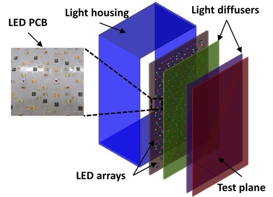
4. LED Solar Simulator Prototype Assembly

Based on the TracePro® simulation results, a LED LASS prototype was constructed as shown in Figure 7. Two six-layer board designs were manufactured with the LEDs surface mounted in the positions defined by the tessellating hexagons of the optical model.
A photograph of the two PCBs loaded with 532 LEDs of ten colors and mounted on a fan-cooled heatsink is shown in Figure 7a. A set of dual-polarity power connections were made to each PCB short side, providing isolated current to each string. An important consideration in the six-layer PCB design was ensuring that all power rails have a sufficient copper conductor cross-section for an appropriate current capacity of each of the 29 individual LED strings, where this was calculated from the recommended forward voltage and current values. A current controller board comprising 29 current control subsystems was used to drive the 29 LED strings on each PCB. The forward voltage was dependent on the numbers of each LED in each string with a supply maximum forward voltage of 36 VDC and forward current of 1000 mA DC for each LED string.
To maintain each LED within the recommended operating temperature range, a set of thermal vias were fabricated through the PCB dielectric layers providing a thermal heat flow path. These thermal vias were placed directly under the LED and mechanically connected the LED thermal pad on the top of the PCB to a large thermal pad located at the bottom of the PCB. This approach produced a cheaper overall PCB design, avoiding the additional cost associated with blind and buried-type thermal conduction approaches. The LED LASS PCBs were in thermal contact with a cooling aggregate heat sink via a 0.5 mm thermally conductive pad on each side of a 5 mm aluminum plate. Figure 7b schematically illustrates the LED LASS modules arranged on the heatsink with the power connection terminals, and the reflective housing mirrors within the aluminum frame, forming a rigid structure. A fan-forced air-cooled heat sink was used for heat dissipation to the room, maintaining system thermal stability, particularly during operation at one-Sun illumination. The actual LED LASS instrument is presented in Figure 7c.

5. Classification and Performance

The design goal for the LED LASS was to achieve a Class AAA solar simulator rating according to the IEC 60904-9, ASTM E-927, and JIS C 8912 standards. These specify the parameters of spectral match (SM), spatial nonuniformity of irradiance (SNI), and temporal instability of irradiance (TIE). The performance parameters of the prototype solar simulator were characterized using the irradiance mapper instrument, operated in an environmentally controlled laboratory at 25 °C.

5.1. Spectral Match (SM)

The spectral characteristics of the light sources used in solar simulation become increasingly important due to the range of solar cell types [37] requiring testing and the different spectral responsivities of these. ASTM G173 [32] defines the standard tables for referencing solar simulator spectral irradiances against the AM1.5G spectrum over 100 nm intervals. The spectral variation was compared against AM1.5G by integrating the total area under the spectral curve between 400 and 1100 nm. The spectral rating considers the fraction of the overall spectral irradiance that falls within the defined 100 nm wavelength range, where this fraction has to be within ±25% of the equivalent fraction for the AM1.5G spectrum over the same interval. The irradiance fraction values and the classification of each interval, as determined by adherence to the standards (IEC 60904-9, ASTM E-927, and JIS C 8912), are listed in Table 3.
Equation (2) [38] is used to evaluate the quality of the LED LASS spectrum by calculating the deviation in the LED LASS spectrum from the desired spectrum (AM1.5G) in six wavelength intervals defined within the solar simulator standards.
Irradance   fraction   λ 1 , λ 2 = λ 1 λ 2 S λ dy λ 1 λ 2 E λ dy
where S(λ) is the irradiance spectrum of the solar simulator and E(λ) is the AM1.5G irradiance spectrum in the wavelength range from λ1 to λ2.

5.2. Spatial Non-Uniformity of Irradiance (SNI)

The SNI is critical for measurement of printed solar cell fingers and the LED LASS design. The 2D irradiance uniformity scans were performed using a spectrometer (Ocean Optics), with a cosine corrector on its entrance port, mounted on orthogonal X and Y axis linear stages under LabVIEW® computer control. The emission was measured with a full spectrum recorded every 3 mm on a grid of 3 mm × 3 mm.
A large set of single-color uniformity maps as well as a ten-color full-spectrum map were recorded and the effect of different diffusers on the uniformity was investigated. The effects of combinations of light diffusers were analyzed in terms of homogeneity and intensity loss over the complete spectrum. The light emitted from each LED light source was mixed on the way from the LED SP to the STP. The recorded spectrum at each location in the test plane is the summation of direct and indirect contributions of the light emitted from the LEDs and reflected from the mirrors. The calculated (SNIC) and measured (SNIM) for each of the 10 selected LED types are listed in Table 4.
The SNI of the dual light diffuser combination measured at 140 mm from the LED SP yielded a value of 1.68%. The different LED configurations at the emitting surface resulted in a distributed light intensity in the center of the test area, preventing the formation of light hot spots; however, there were edge effects observed in the periphery of the irradiated area. The measured irradiance uniformity map for the LED LASS system using two diffusers is shown in Figure 8.
The design objectives for the multi-PCB solar simulator system were to replicate the performance specification of the LASS PCB unit including the uniformity of irradiance and the spectral distribution of the radiation incident on the STP. It is noticeable from the size of the uniform area (640 cm2) and the value of the SNI that a tessellating system of larger area was achievable from assembling multi-unit LASS PCBs. No defects in uniformity were observed from extending the source area. The current design allows any number of boards to be arrayed longitudinally, without gaps between the boards; however, the electrical connection, when arraying laterally, required a gap. Therefore, a series of TracePro® simulations were run by varying the distance between the PCBs in the Y direction, with the results showing that a 5–10 mm gap between the PCBs laterally retained a Class A SNI.

5.3. Temporal Instability of Irradiance (TIE)

As a semiconductor junction device, LEDs establish a temperature-dependent steady-state distribution of electrons and holes in the conduction and valence bands, as well as the energy gap between the bands, requiring an initial warm-up period for stable operation. This behavior is expected and manifests as an emission shift and an intensity signal drop. The thermal conductivity of the LED structures, the PCB thermal vias, and coupling to the air-cooled heat sink structures dictate the initial warm up time of 5 min (Figure 9a). The measured long-term TIE was <0.1% over a 30-min interval and the short-term TIE was below 0.01% over a 1.5-s period. A slower drift due to ambient is apparent in Figure 9b where a <0.5% variation in the light intensity was observed over 550 min of continuous operation at 100 mW/cm2.

6. Current-Voltage Diagnostic Test

In current–voltage (I–V) characteristic measurements, the mismatch is used to correct the difference between the measured short-circuit current (ISC) of a test cell under solar simulator illumination and the ISC of the same cell under the reference spectrum [38]. This mismatch can be caused either by differences between the reference photovoltaic device and test device quantum efficiencies or the test solar simulator spectral irradiance distribution and the reference spectral irradiance distribution by which the reference cell was calibrated [39].
Practically, a set of calibrated reference cells and test cells were used to determine the electrical performance of photovoltaic cells under the simulated sunlight. A calibrated silicon reference cell (Oriel Part Number: 91150V) was used to adjust the light intensity of both simulators by matching the one-sunlight (100 mW/cm2) short-circuit current for both light sources in accordance with the requirements for photovoltaic reference devices IEC 60904-2 [40]. To meet the standard requirements of the I–V electrical performance measurements, a large-area xenon-based (Abet Technologies, Model: 11044) solar simulator was used. To minimize measurement errors introduced by temperature fluctuations, both the test and reference cells were maintained at room temperature 25 °C during the test [41].
I–V sweeps were performed on silicon and organic photovoltaic test cells. The ISC were matched to compare equivalent light intensities between the two light sources. Open-circuit voltage (VOC), fill factor (FF), and power conversion efficiency (PCE) were measured to quantify any noticeable variances between the two light sources. The electrical parameters extracted from I–V curves for the two sets of solar cells were closely matched and the I–V curves overlapped, as shown in Figure 10a,b. Although the xenon-based solar simulator and the LED LASS spectra do not have identical spectral output, they closely match in overall irradiance from 350 to 1100 nm. As such, no major differences were detected in the I–V tests, despite the spectral variation between the two light sources. Indeed, the obtained characteristic properties of the I–V curve response produced from the two simulators were very similar under matched short-circuit current conditions and all measurement variances were within the measurement variability.
Table 5 compares the ISC, VOC, FF, and PCE between the LED LASS system and xenon solar simulator. The spectral differences between the xenon-based and LED-based solar simulator, in this instance, did not affect the characteristic curve responses for the tested modules.
This similarity in I–V curve response for Si and OPV cells is clear evidence of the very good performance of the LASS system. The ISC generated in the same cell tested using both solar simulators indicates only insignificant values (~≤1%) of the absolute fractional differences (|Δ|) between the metrics used to characterize solar cell performance.

7. Conclusions

The design principles of a large-area LED-based solar simulator were discussed in the context of sophisticated optical modeling of the emission from 266 LEDs that formed the spatial and spectral basis of the device. Beginning with a repeating hexagonal pattern, a rectangular shape was extracted that allows lateral replication to form a continuously uniform light source with spectral and spatial adherence to the solar radiation standards. The optimal housing and diffuser designs were determined through the optical modelling. The spatial arrangements of the LEDs formed the basis of the printed circuit board design, and the housing and diffuser designs determined the physical dimensions and structure of the prototype constructed. The LASS system was built and the output was evaluated for more than 500 h of continuous running at one-Sun illumination level. The spectral range covered was 350–1100 nm to account for photovoltaic technologies with a wide spectral response. The new-design artificial light source emission was classified as Class AAA according to ASTM, IEC, and JIS solar simulator standards. A new standard is essential to stipulate the spectral performance and irradiance uniformity classification of the new generation of solar simulators, particularly when measuring non-silicon PV devices. LED technology offers new possibilities for large-area solar simulation, and extending the spectral range below 400 nm and above 1100 nm may be achieved by simply adding more LED colors in any new LED solar simulator design.

Author Contributions

Conceptualization and supervision, A.A.-A., J.H., B.V., X.Z., W.B. and P.D.; investigation, A.A.-A.; resources, COE and ANFF Facility; writing—original draft preparation, A.A.-A.; writing—review and editing, J.H., B.V., X.Z., W.B. and P.D. All authors have read and agreed to the published version of the manuscript.

Funding

This work was supported by the University of Newcastle through the Centre for Organic Electronics.

Institutional Review Board Statement

Not applicable.

Informed Consent Statement

Not applicable.

Data Availability Statement

Not applicable.

Acknowledgments

The work was also performed in part at the Material Node of the Australian National Fabrication Facility under the National Collaborative Research Infrastructure Strategy to provide nanofabrication and microfabrication facilities for Australia’s researchers.

Conflicts of Interest

The authors declare no conflict of interest.

Abbreviations

SiSilicon solar cell
PVPhotovoltaic
LEDLight emitting diode
PCBPrinted circuit board
AM1.5GThe air mass 1.5 is the global standard spectrum
IECInternational Electrotechnical Commission
ASTMAmerican Society for Testing and Materials
JISJapanese Industrial Standard
IRInfrared light
Class AAAClass A solar simulator has the highest-level classification within ±25% difference in the spectral match to the Sun irradiance, <2% variant in spatial non-uniformity of irradiance, and <2% variation in temporal instability of irradiance with the time.
LASSLarge area solar simulator
UVUltraviolet light
KKelvin
LED SPLED source plane
STPSample test plane
SNISpatial non-uniformity of irradiance
Emax and EminMaximum and minimum irradiance values
SMSpectral match
TIETemporal instability of irradiance
I-VCurrent-Voltage characteristic
OPVOrganic photovoltaic
PCEPower conversion efficiency
ISCShort circuit current
VOCOpen circuit Voltage
FFFill factor

References

  1. D’Alessandro, C.; De Maio, D.; Mundo, T.; Musto, M.; Di Giamberardino, F.; Monti, M.; Dalena, D.; Palmieri, V.G.; De Luca, D.; Di Gennaro, E.; et al. Low cost high intensity LED illumination device for high uniformity solar testing. Sol. Energy 2021, 221, 140–147. [Google Scholar] [CrossRef]
  2. Vallon, M.; Gao, L.; Jiang, F.; Krumm, B.; Nadolny, J.; Song, J.; Leisner, T.; Saathoff, H. LED-based solar simulator to study photochemistry over a wide temperature range in the large simulation chamber AIDA. Atmos. Meas. Tech. 2022, 15, 1795–1810. [Google Scholar] [CrossRef]
  3. Watjanatepin, N.; Sritanauthaikorn, P. Rectangular module for large scale solar simulator based on high-powered LEDs array. Telkomnika Telecommun. Comput. Electron. Control 2022, 20, 462–474. [Google Scholar] [CrossRef]
  4. Sun, C.; Jin, Z.; Song, Y.; Chen, Y.; Xiong, D.; Lan, K.; Huang, Y.; Zhang, M. LED-based solar simulator for terrestrial solar spectra and orientations. Sol. Energy 2022, 233, 96–110. [Google Scholar] [CrossRef]
  5. 60904-9 Ed. 3.0 b:2020; I.E.C. Photovoltaic Devices—Part 9: Classification of Solar Simulator Characteristics. International Electrotechnical Commission: Geneva, Switzerland, 2020.
  6. E927-19; A.S.T.M. Standard Classification for Solar Simulators for Electrical Performance Testing of Photovoltaic Devices. ASTM International: West Conshohocken, PA, USA, 2019.
  7. C 8912:1998/AMENDMENT 2:2011; J.I.S. Solar Simulators For Crystalline Solar Cells And Modules (Amendment 2) (Foreign Standard). Japanese Standards Association: Tokyo, Japan, 2011.
  8. Esen, V.; Sağlam, Ş.; Oral, B. Light sources of solar simulators for photovoltaic devices: A review. Renew. Sustain. Energy Rev. 2017, 77, 1240–1250. [Google Scholar] [CrossRef]
  9. Eddy, R. Design and Construction of the 15-ft-Beam Solar Simulator SS15B; NASA: Washington, DC, USA, 1969; pp. 52–57. [Google Scholar]
  10. Linden, K.J.; Neal, W.R.; Serreze, H.B. Adjustable spectrum LED solar simulator. In Proceedings of the SPIE OPTO, San Francisco, CA, USA, 27 February 2014; pp. 900317–900319. [Google Scholar]
  11. Namin, A.; Jivacate, C.; Chenvidhya, D.; Kirtikara, K.; Thongpron, J. Determination of solar cell electrical parameters and resistances using color and white LED-based solar simulators with high amplitude pulse input voltages. Renew. Energy 2013, 54, 131–137. [Google Scholar] [CrossRef]
  12. Al-Ahmad, A.Y.; Clark, D.; Holdsworth, J.L.; Vaughan, B.; Belcher, W.J.; Dastoor, P.C. An Economic LED Solar Simulator Design. IEEE J. Photovolt. 2022, 12, 521–525. [Google Scholar] [CrossRef]
  13. Kohraku, S.; Kurokawa, K. A fundamental experiment for discrete-wavelength LED solar simulator. Sol. Energy Mater. Sol. Cells 2006, 90, 3364–3370. [Google Scholar] [CrossRef]
  14. Tsuno, Y.; Koichi, K.; Kurokawa, K. New generation of PV module rating by LED solar simulator—A novel approach and its capabilities. In Proceedings of the 33rd IEEE Photovoltaic Specialists Conference, San Diego, CA, USA, 11–16 May 2008; pp. 1–5. [Google Scholar]
  15. Bliss, M.; Betts, T.R.; Gottschalg, R. An LED-based photovoltaic measurement system with variable spectrum and flash speed. Sol. Energy Mater. Sol. Cells 2009, 93, 825–830. [Google Scholar] [CrossRef] [Green Version]
  16. Martin, B.; Thomas, S.W.; Betts, R.; Gottschalg, R. Towards A High Power, All Led Solar Simulator Closely Matching Realistic Solar Spectra. In Proceedings of the 24th European Photovoltaic Solar Energy Conference, Hamburg, Germany, 21–25 September 2009. [Google Scholar]
  17. Kolberg, D.; Schubert, F.; Lontke, N.; Zwigart, A.; Spinner, D.M. Development of tunable close match LED solar simulator with extended spectral range to UV and IR. Energy Procedia 2011, 8, 100–105. [Google Scholar] [CrossRef]
  18. Kolberg, D.; Schubert, F.; Klameth, K.; Spinner, D.M. Homogeneity and Lifetime Performance of a Tunable Close Match LED Solar Simulator. Energy Procedia 2012, 27, 306–311. [Google Scholar] [CrossRef] [Green Version]
  19. Hamadani, B.H.; Chua, K.; Roller, J.; Bennahmias, M.J.; Campbell, B.; Yoon, H.W.; Dougherty, B. Towards realization of a large-area light-emitting diode-based solar simulator. Prog. Photovolt. Res. Appl. 2012, 21, 779–789. [Google Scholar] [CrossRef]
  20. Novičkovas, A.; Baguckis, A.; Mekys, A.; Tamošiūnas, V. Compact light-emitting diode-based AAA class solar simulator: Design and application peculiarities. IEEE J. Photovolt. 2015, 5, 1137–1142. [Google Scholar] [CrossRef]
  21. Yang, C.; Wang, J.; Guo, X.; Wang, Y.; Ding, Z. A multisource regular dodecahedron solar simulator structure for uniform flux. IEEE J. Photovolt. 2016, 6, 516–521. [Google Scholar] [CrossRef]
  22. Watjanatepin, N. Design Construct and Evaluation of Six-Spectral LEDs-Based Solar Simulator Based on IEC 60904-9. Int. J. Eng. Technol. (IJET) 2017, 9, 923–931. [Google Scholar] [CrossRef] [Green Version]
  23. López-Fraguas, E.; Sánchez-Pena, J.M.; Vergaz, R. A low-cost LED-based solar simulator. IEEE Trans. Instrum. Meas. 2019, 68, 4913–4923. [Google Scholar] [CrossRef]
  24. Vedat, E.; Saglam, S.; Oral, B.; Esen, O.C. Spectrum Measurement of Variable Irradiance Controlled LED-Based Solar Simulator. Int. J. Renew. Energy Res. (IJRER) 2020, 10, 109–116. [Google Scholar]
  25. Hofbauer, J.; Rudolph, M.; Streif, S. Stabilising the Light Spectrum of LED Solar Simulators Using LQG Control. IFAC-Pap. 2020, 53, 6583–6590. [Google Scholar] [CrossRef]
  26. Meshram, N.; Yadav, P. Design of a Low Cost Solar Simulator by using Light Emitting Diode (LED). Proc. J. Phys. Conf. Ser. 2021, 1921, 012103. [Google Scholar] [CrossRef]
  27. Song, J.-Y.; Zeng, R.-M.; Xu, D.-Y.; Wang, Y.; Ding, Z.; Yang, C. A compact AAA-compatible multispectral solar simulator based on spherical cap chamber. Sol. Energy 2021, 220, 1053–1064. [Google Scholar] [CrossRef]
  28. Cortés-Severino, R.; Cárdenas-Bravo, C.; Barraza, R.; Sánchez-Squella, A.; Valdivia Lefort, P.; Castillo-Burns, F. Optimal design and experimental test of a solar simulator for solar photovoltaic modules. Energy Sci. Eng. 2021, 9, 2514–2528. [Google Scholar] [CrossRef]
  29. Vosylius, Ž.; Novičkovas, A.; Laurinavičius, K.; Tamošiūnas, V. Rational Design of Scalable Solar Simulators With Arrays of Light-Emitting Diodes and Double Reflectors. IEEE J. Photovolt. 2022, 12, 512–520. [Google Scholar] [CrossRef]
  30. Tavakoli, M.; Jahantigh, F.; Zarookian, H. Adjustable high-power-LED solar simulator with extended spectrum in UV region. Sol. Energy 2021, 220, 1130–1136. [Google Scholar] [CrossRef]
  31. Bartela, Ł.; Stanek, B.; Węcel, D.; Skorek-Osikowska, A. A solar simulator numerical modeling for heat absorption phenomenon research in a parabolic trough collector. Int. J. Energy Res. 2021, 46, 10074–10087. [Google Scholar] [CrossRef]
  32. ASTM G173-03(2012); Standard Tables for Reference Solar Spectral Irradiances: Direct Normal and Hemispherical on 37° Tilted Surface. ASTM International: West Conshohocken, PA, USA, 2012; p. 37.
  33. Laaber, D. Solar Simulators. In Solar Thermal Energy; Springer: New York, NY, USA, 2022; pp. 215–243. [Google Scholar]
  34. Al-Ahmad, A.Y.; Holdsworth, J.; Vaughan, B.; Sharafutdinova, G.; Zhou, X.; Belcher, W.J.; Dastoor, P.C. Modular LED arrays for large area solar simulation. Prog. Photovolt. Res. Appl. 2019, 27, 179–189. [Google Scholar] [CrossRef]
  35. Sekiguchi, Y.; Konno, A.; Tsumura, M. Design method for a thin uniform direct backlight using a diffuser plate with a pattern on the surface and optical films. Appl. Opt. 2015, 54, 482–491. [Google Scholar] [CrossRef]
  36. Solgaard, O. Photonic Microsystems: Micro and Nanotechnology Applied to Optical Devices and Systems; Springer Science & Business Media: Berlin/Heidelberg, Germany, 2009. [Google Scholar]
  37. Napat Watjanatepin, P.S. Large Scale LED-Modular-Based Solar Simulator and Calibration Method for PV-Module Characterization. J. Hunan Univ. Nat. Sci. 2021, 48, 474–484. [Google Scholar]
  38. Scherff, M.L.; Nutter, J.; Fuss-Kailuweit, P.; Suthues, J.; Brammer, T. Spectral mismatch and solar simulator quality factor in advanced LED solar simulators. Jpn. J. Appl. Phys. 2017, 56, 08MB24. [Google Scholar] [CrossRef] [Green Version]
  39. Schubert, F.; Spinner, D. Solar Simulator Spectrum and Measurement Uncertainties. Energy Procedia 2016, 92, 205–210. [Google Scholar] [CrossRef]
  40. IEC 60904-2:2015; Photovoltaic Devices—Part 2: Requirements for Photovoltaic Reference Devices. International Electrotechnical Commission: Geneva, Switzerland, 2015.
  41. ASTM E1362-15; Standard Test Methods for Calibration of Non-Concentrator Photovoltaic Non-Primary Reference Cells. ASTM International: West Conshohocken, PA, USA, 2019.
Figure 1. (a) The spectral irradiance of the 10 individual LED types (365 nm, 385 nm, 470 nm, 505 nm, 655 nm, 740 nm, 850 nm, 940 nm, 5600 K, and 3000 K), each with unique spectral profile. (b) The spectral irradiance of the Sun AM1.5G (gray) set against the synthetic spectrum of the LED LASS (black).
Energies 15 08393 g001
Figure 2. (a) One hexagon module loaded with 71 LEDs of ten colors. (b) The optimized layout of the 10 distinct color LEDs inside the 50 mm side-length hexagonal unit. (c) The number of LEDs and the corresponding arrangement for each individual LED light source inside the hexagonal unit (365 nm: 6 LEDs, 385 nm: 8 LEDs, 470 nm: 6 LEDs, 505 nm: 6 LEDs, 655 nm: 6 LEDs, 740 nm: 6 LEDs, 850 nm: 4 LEDs, 940 nm: 6 LEDs, 5600 K: 10 LEDs, and 3000 K: 13 LEDs).
Energies 15 08393 g002
Figure 3. (a) The base hexagon unit cell. (b) Combined two-unit cell. (c) Extraction of a 30 cm × 8.7 cm rectangular printed circuit board from a 12-unit cell array.
Energies 15 08393 g003
Figure 4. (a) The LED LASS modular arrangement as modeled in the TracePro® software. The light housing is shown in blue, the LED arrays are on the SP, the two light diffusers are shown in green and brown, and the sample test plan is shown in red. (b) The light enclosure designed with dual diffuser stages illustrates the light mixing stages to improve the SNI at the STP by two diffusers: a prismatic patterned (Diffuser1) and micro-structured (Diffuser 2). The side mirrors enhance the uniformity by reflecting the secondary rays toward diffuser 2.
Energies 15 08393 g004
Figure 5. The irradiance maps (a) of different ray numbers (from 1 k to 1 M rays); the color scale bar shows the irradiance between 0% and 100% of the maximum irradiances. (b) The maximum flux intensity and the nonuniformity of irradiance as a function of ray numbers.
Energies 15 08393 g005
Figure 6. (a) Plotted SNI against test plane distance. Error bars are calculated from the standard deviation of simulation results. (b) The modeled irradiance map of 532 LED emissions from 10 LED colors mounted in a housing with internal mirrors. The color scale bar shows the irradiance between 0% and 100% of the maximum irradiance.
Energies 15 08393 g006
Figure 7. (a) Photograph of two aligned PCBs loaded with 532 LEDs of ten colors, mounted on a fan-cooled heatsink to create a larger area unit. (b) Schematic illustration of the LED LASS unit arranged on the heatsink with the location of the power connection terminals, the mirrors, and the construction of the aluminum frame. (c) The actual LED LASS instrument.
Energies 15 08393 g007
Figure 8. The measured irradiance uniformity map for a dual PCB LED LASS system using two diffusers: one, P-PY01, at 40 mm and the second one, C-CHH 30, at 140 mm from the LED SP. Class AAA performance is achieved in the red zone.
Energies 15 08393 g008
Figure 9. (a) The changes in light intensity during the warming-up period of 30 min utilizing a 250-millisecond data acquisition time. (b) The irradiance from the LED LASS system as a function of time for 550 min of continuous operation; the measurements were recorded after stabilizing the system for 5 min. The blue dotted lines represent the Class A upper and lower limits of (±2%).
Energies 15 08393 g009
Figure 10. The IV curves of two types of solar cell tested under the xenon and LED solar simulator: (a) silicon and (b) large-area 26 cm × 16 cm printed OPV array.
Energies 15 08393 g010
Table 1. The advantages and disadvantages of common solar simulator light sources.
Light SourceAdvantageDisadvantage
Xenon arc
lamp
High output irradiance, very good spectral match to natural sunlight (AM1.5), and stable over time.High cost, short life (1500–2500 h), requires an expensive power supply, irradiance peaks shift slightly to the IR as the lamp ages, and small illumination area.
Metal halide
lamp
High output power, relatively inexpensive, large illumination area with multiple lamps, and relatively long life (6000–15,000 h).Low collimation quality, high power consumption, dense UV emission, and low irradiance uniformity.
High-pressure
sodium lamp
High luminous efficacy, broad spectrum range, long life (12,000 h), and low cost. Needs optical filter, low level (IR and UV emission), limited useful emission band (500–700 nm), and intense spectral emission lines.
Fluorescent
lamp
Inexpensive, perfect for large-area illumination with multiple lamps, cheap and easy to maintain, and long rated lifespan of (7000–15,000 h).Low light intensity, low collimation quality, limited light-band emission (300–750 nm), poor spectral match, and low irradiance uniformity.
Sulfur plasma lampHigh luminous efficacy, full-spectrum visible light in wavelength range of 400–700 nm (high-quality white light), long rated lifespan of (30,000 h), low power consumption, and can be efficiently distributed over large spaces.Low-uniformity intensity distribution, limited spectrum range (380–700 nm), produces almost no ultraviolet light and very little infrared, and intensity decreases rapidly under continuous operation.
Quartz tungsten
halogen lamp
Strongly infrared emission, economical (small, lightweight, cheap), low power consumption, smooth spectral emission, and stable output emission.Maximum color temperature of 3600 K, overheating, limited output power in the visible-spectrum range, and lifetime depends on operating voltage and rated wattage (2500 h).
Light-emitting diodeLow cost, high output power, low energy consumption, great color ranges, direction emission, and dimming capability with instantaneous on/off functionality, perfect for large-area illumination, long lifetime (100,000 h), environmentally friendly, small footprint, and operating in very low voltage. Individual emitters with narrow spectral emission and limited spectral range (270–1200 nm).
Optical design required to homogenize spectral match uniformity and uniformity of irradiance.
Table 2. Characteristics of the 10 selected LED types for one hexagon module solar simulator.
Wavelength (nm)LED TypePower/FluxPart NumberLED #
350–380365 nm655 (mW)LTPL-C034UVH3656
370–410385 nm975 (mW)LTPL-C034UVH3858
415–7803000 K95 (Im)LX 18-P130-36
410–7805600 K220 (Im)LXML-PWC1-012013
460–520470 nm40 (Im)LXML-PBO1-004010
470–550505 nm65 (Im)LXMLPE0100706
620–680655 nm360 (mW)LXM3-PDOI6
700–780740 nm705 (mW)LZl-OOR3026
820–920850 nm770 (mW)SFH 4715A4
920–1100940 nm425 (mW)SFH 4725S6
Table 3. LED LASS prototype irradiance and integrated target spectral irradiance ratios.
Wavelength Interval (nm)[%] of LED
Irradiance
SM [%] to ASTMSM [%] to IEC & JSCClass
400–50017.0793.7492.77A
500–60020.56104.21103.32A
600–70018.41101.15100.05A
700–80013.9894.5293.83A
800–90012.46100.5699.68A
900–110015.2095.6695.60A
Table 4. Calculated and measured SNI for each of the 10 selected LED types.
365 nm385 nm470 nm505 nm655 nm740 nm850 nm940 nm5600 K3000 KAll
SNIC (%)2.32.91.91.82.72.42.72.82.92.12.0
SNIM (%)2.12.71.81.72.52.32.52.42.62.01.9
Table 5. Comparative values for Si and OPV cells under test.
Cell TypeMetricPCE (%)VOC (V)ISC (mA)FF
SiXenon7.227.20−3210.668
LED7.257.26−3180.669
|Δ|0.990.991.000.99
OPVXenon1.1210.0−32.60.311
LED1.1310.6−32.10.308
|Δ|0.990.941.021.00
Publisher’s Note: MDPI stays neutral with regard to jurisdictional claims in published maps and institutional affiliations.

