Article

Single-Phase Five-Level Multilevel Inverter Based on a Transistors Six-Pack Module

by
Flavio A. Garcia-Santiago
1,
Julio C. Rosas-Caro
2,*,
Jesus E. Valdez-Resendiz
3,
Jonathan C. Mayo-Maldonado
4,
Antonio Valderrabano-Gonzalez
2,* and
Hector R. Robles-Campos
2
1
CERREY S.A. de C.V., Av. República Mexicana #300, San Nicolás de los Garza 66450, Mexico
2
Facultad de Ingeniería, Universidad Panamericana, Alvaro del Portillo 49, Zapopan 45010, Mexico
3
Faculty of Engineering, Tecnologico de Monterrey, Av. Eugenio Garza Sada 2501, Monterrey 64849, Mexico
4
Department of Electronic and Electrical Engineering, The University of Sheffield, Sheffield S102TN, UK
*
Authors to whom correspondence should be addressed.
Submission received: 14 October 2022 / Revised: 29 November 2022 / Accepted: 5 December 2022 / Published: 9 December 2022
(This article belongs to the Special Issue Modeling, Control and Design of Power Electronics Converters)

Abstract

:
This article introduces a single-phase five-level multilevel inverter based on six switches and two transformers. The proposed converter requires a single dc input source with low voltage. The disposition of switches makes it possible to build the converter with a transistors six-pack module off-the-shelves, traditionally used to build three-phase inverters, which simplifies the manufacturing process. The converter increases the voltage with two transformers; for that reason, it does not require an auxiliary step-up converter. The use of transformers (with the transformer’s turns ratio) allows for using the same topology for several input voltage levels. To verify the operation of the proposed multilevel inverter, a computer-based simulation was performed with PSIM, a software that considers parasitic components. The results show that the proposed converter can work properly.

1. Introduction

Power electronics has become a key technology for renewable energy applications, electric and hybrid electric vehicles, and the advancement of electric and electronic appliances. One of the most recent advances in power electronics has been the development of multilevel inverters (MLI) [1,2,3,4,5]. They are already an established solution for developing medium- and high-power electronics applications. MLI has been applied in applications of ac-dc rectification, dc-ac inversion, dc-dc conversion, and as variable speed drives with combined conversion schemes (i.e., dc-ac-dc) [6,7].
Some of the advantages of high-power MLI are: (i) The output voltage is provided in a stepped output function that can be filtrated with smaller components than a two-level output; for this reason, MLI are considered to have a good power quality, for example, in the case of their application as an active front end (AFE) rectifier, the input current has low harmonic distortion. (ii) Low-voltage stress on devices, as will be further discussed, in low-voltage applications is not a big problem, but in high-voltage applications, this is a major concern. Their capability to operate with a relatively high-power quality and a relatively low switching frequency leads to high efficiency and small magnetic components [6,7,8].
The first three topologies studied as MLI were: (i) neutral point clamped or diode clamped [9,10,11], (ii) the flying capacitor topology [12,13], and (iii) cascaded cells’ topology [1,2,3,4,5,6,7]. Recently, the (iv) modular multilevel converter (MMC) [14,15,16] has proven to have many advantages and can be considered the fourth topology of the main family of converters, for which the main characteristics are their applications in high-power applications.
There is another kind of MLI topologies, where the main applications are low-power converters, and they are characterized by having a larger number of output voltage levels (compared to the high-power ones) with a relatively reduced number of switches. In this article, we will call high-voltage MLI (HV-MLI) the converters of the first family and low-voltage MLI (LV-MLI) the converters of the second family.
The HV-MLI are applied in applications such as variable speed drives for large motors, static VAR generators, and grid-tied applications [1,2,3,4,5,6,7,8]. They can be used to make flexible ac transmission systems (FACTS) and power conditioners [17], and renewable energy applications [17,18,19].
The first member of the family of MLI was the neutral point-clamped or diode-clamped converter, initially introduced in [9]. Its basic configuration is shown in Figure 1a. Figure 1b shows the basic configuration of the flying capacitor MLI.
The main advantage of the HV-MLI over the LV-MLI for medium- to high-power applications is that an HV-MLI has the same voltage stress on all switches, which is only a fraction of the output voltage. On the other hand, topologies of LV-MLI usually have a larger ratio of output voltage levels over the number of switches. Still, they usually have a larger ratio of voltage stress on devices over the output voltage. Furthermore, for low-voltage applications, HV-MLI has some limitations. Topologies with several voltage sources are more expensive than other low-voltage solutions (i.e., the traditional full-bridge inverter) since they require more than one input voltage source and require isolation among them. Topologies with a single voltage source usually require an additional mechanism to balance the voltage in capacitors.
This article introduces a single-phase five-level multilevel inverter based on six switches and two transformers. The proposed converter requires a single dc input source with low voltage, which is an advantage since no voltage balancing mechanisms are required. The disposition of switches makes it possible to build the converter with the widely known transistors six-pack modules since those packages are commercially available (off-the-shelves), and their use simplifies the manufacturing process. The converter increases the voltage with two transformers, for which the converter does not require an auxiliary step-up converter. The proposed converter features low-voltage stress on transistors. The main drawbacks are: (i) it uses two transformers; however, this allows using the same topology for several input voltage levels by changing the transformers’ turn ratio, and (ii) if the switching method used is the line switching frequency, it requires an auxiliary boost converter to regulate the output voltage. Despite the requirements of an auxiliary converter to regulate the output voltage, most of the voltage gain can be performed with the transformer’s turn ratios.
To verify the operation of the proposed multilevel inverter, a computer-based simulation was performed with PSIM, a software that considers parasitic components. The results show that the proposed converter can work properly.

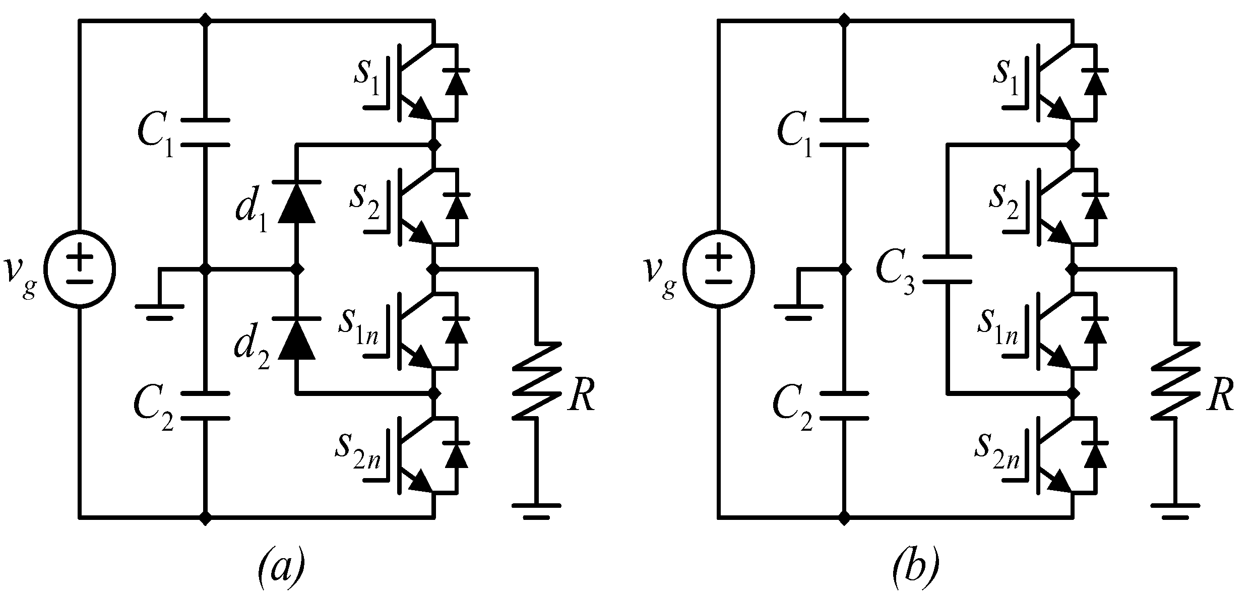
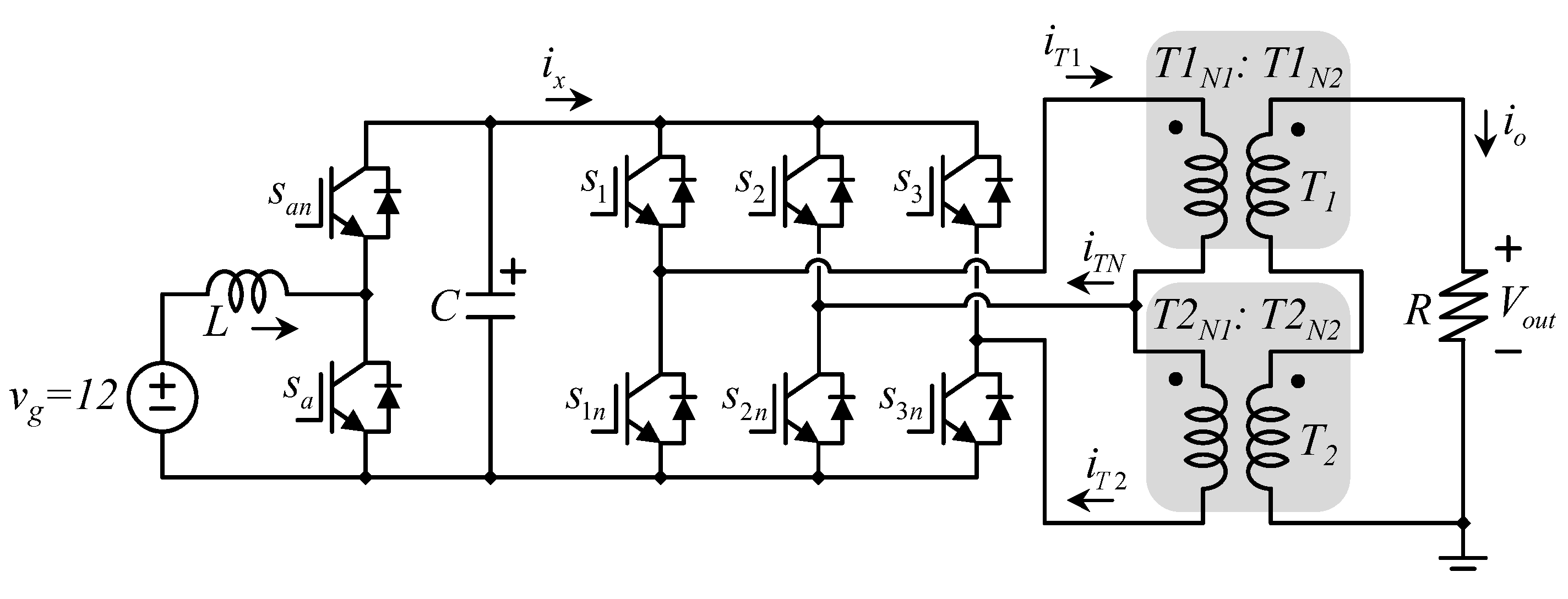
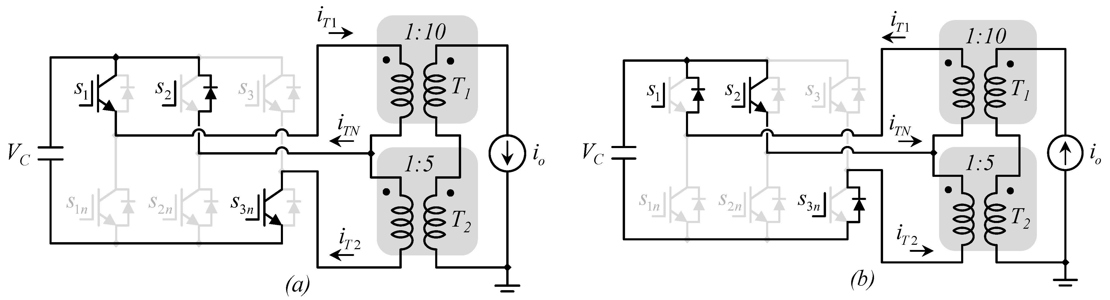
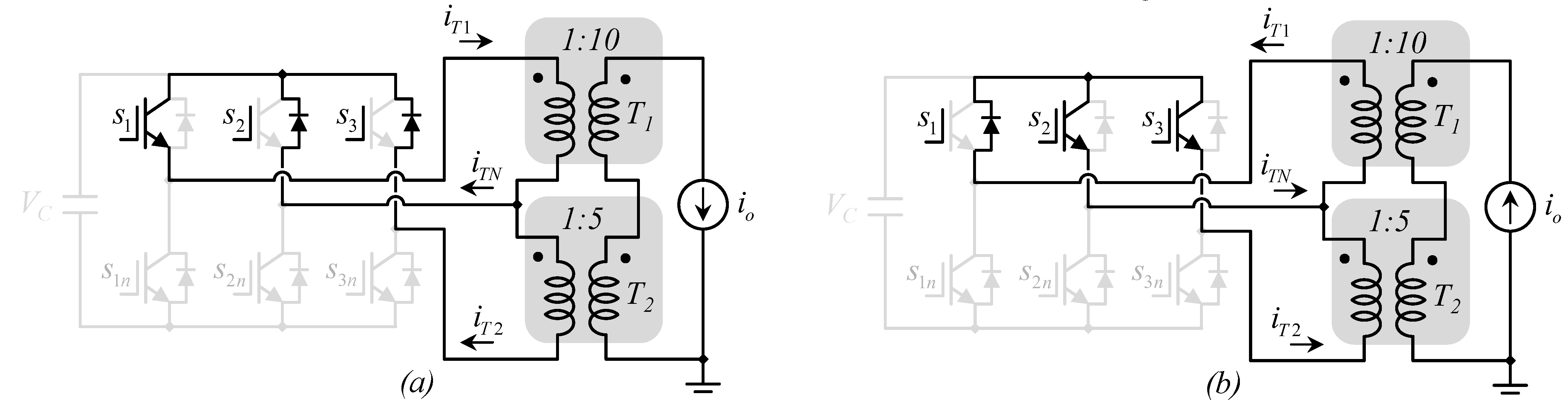
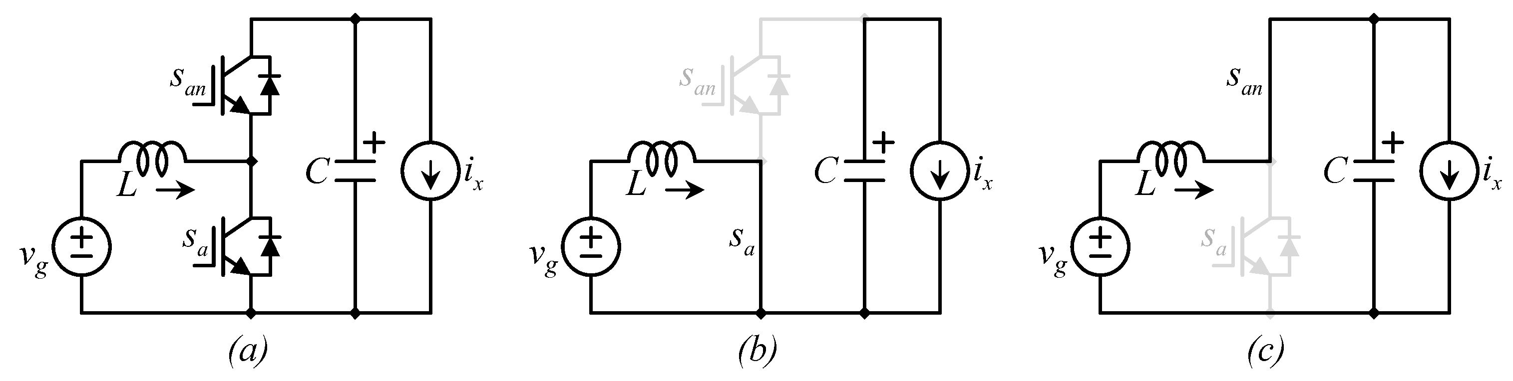
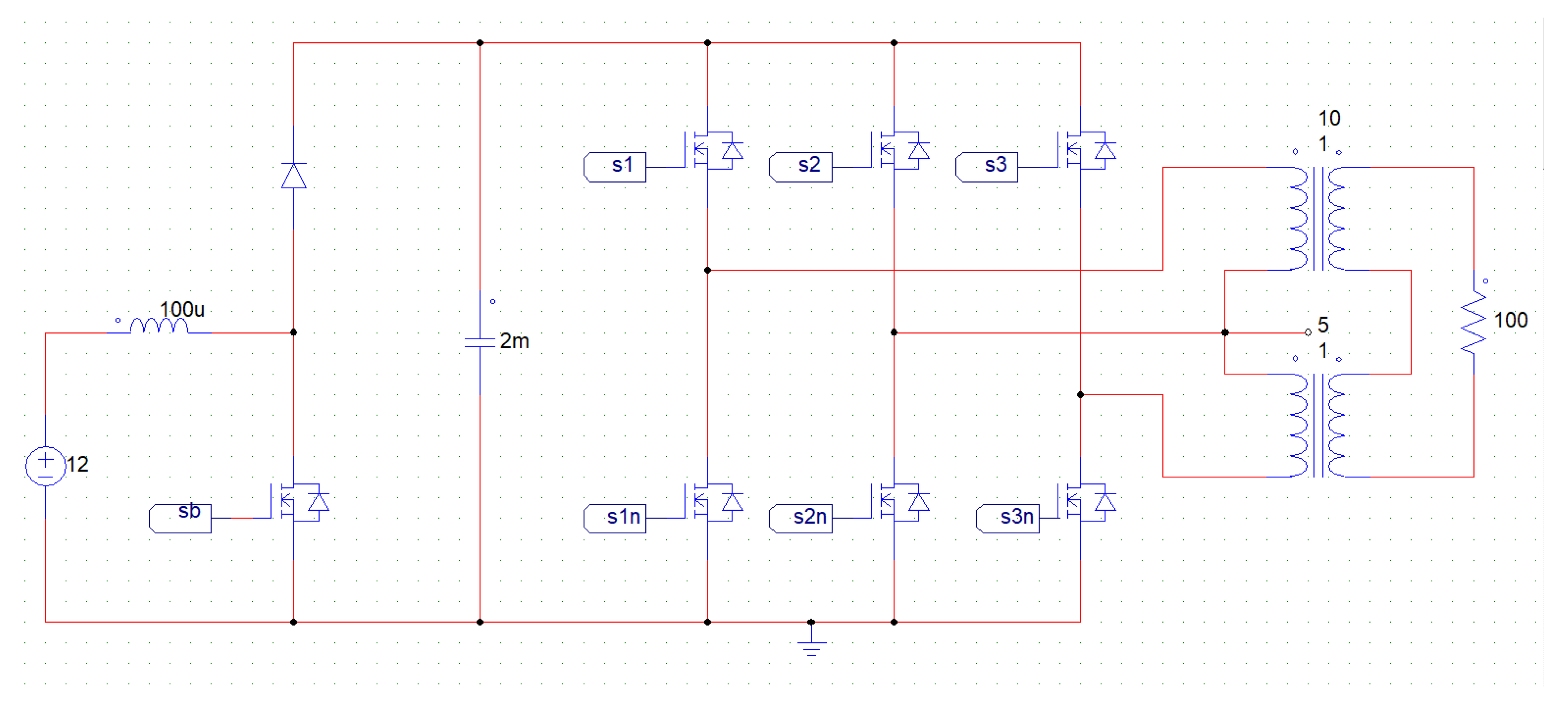
2. The Proposed Topology

As mentioned before, the core of the switching stage is a full bridge or six-pack module of MOSFETS or IGBTs. Those six-pack modules are widely used to build low-power three-phase inverters (two levels); in this case, the inverter is a single-phase five-level inverter. Figure 2 shows a commercial six-pack module, indicating the output phases and dc input side, and the small connectors at the top are for gate drivers (a pair for each transistor).
Figure 3 shows the proposed five-level single-phase inverter in a full application. As mentioned before, the inverter requires its input to be regulated, and in this case, a dc-dc boost converter is used to regulate the voltage (an interleaved boost may be used if a large amount of power is handled).
The six-pack is made, in this case, by s1, s2, s3, s1n, s2n, and s3n. The six-pack switching stage feeds two single-phase transformers, T1 and T2. The turn ratio can be selected according to the desired input and output voltage, and this can be customized according to the application. Let us consider that the power converter is made of a pre-regulator (boost converter), which is fed with a 12 V dc input. The boost converter regulates the voltage to feed the six-pack with 18 V and the inverter must generate a 127 V ac voltage (180 V peak). T1 may have (for this example) a turn ratio of 1:10, while T2 has a turn ratio of 1:5.
The six transistors are driven with three switching signals, and usually the two transistors of the same arm are complementary. The name of the transistors was assigned considering this. For example, s1 is complementary to s1n. When s1 is closed, s1n is open, and vice versa. This simplifies the description of the firing signals. We can describe the behavior with only three switching signals, considering that the other three are complementary. For the analysis, only the upper switching signals are described since the lower switches are the logical inverse of the upper ones.
The principle of operation of the proposed circuit can be explained in the following manner. If there are three firing signals that can take two possible states (zero or one), there is a total of eight possible switching states. The instantaneous output voltage depends on the state of the transistors, and each transformer can contribute with a positive, negative, or zero voltage to the output, depending on how its primary winding is connected to the input voltage source.
Let us analyze the eight switching states one by one. We will consider the input voltage is the output of the boost converter, and it is regulated to 18 V, and the turn ratio of transformers is 1:10 for T1 and 1:5 for T2. Parameters may change depending on the applications, but it will help to explain the principle of operation.
From Figure 3, we can define the primary winding currents in terms of the output current and the transformer’s turn ratio as in (1)–(3):
i T 1 = T 1 N 2 T 1 N 1 i o .
i T 2 = T 2 N 2 T 2 N 1 i o .
i T N = i T 1 i T 2 = T 1 N 2 T 1 N 1 T 2 N 2 T 2 N 1 i o .
Let us consider, for example, the input voltage of the transistor six-pack is the output of the boost converter, and it is regulated to 18 V. In this case, all transistors are rated to 18 V. Their current depends on two different factors, the loads’ power factor and the switching state. Below, each switching state is analyzed to gain a better idea of the current through the switches.

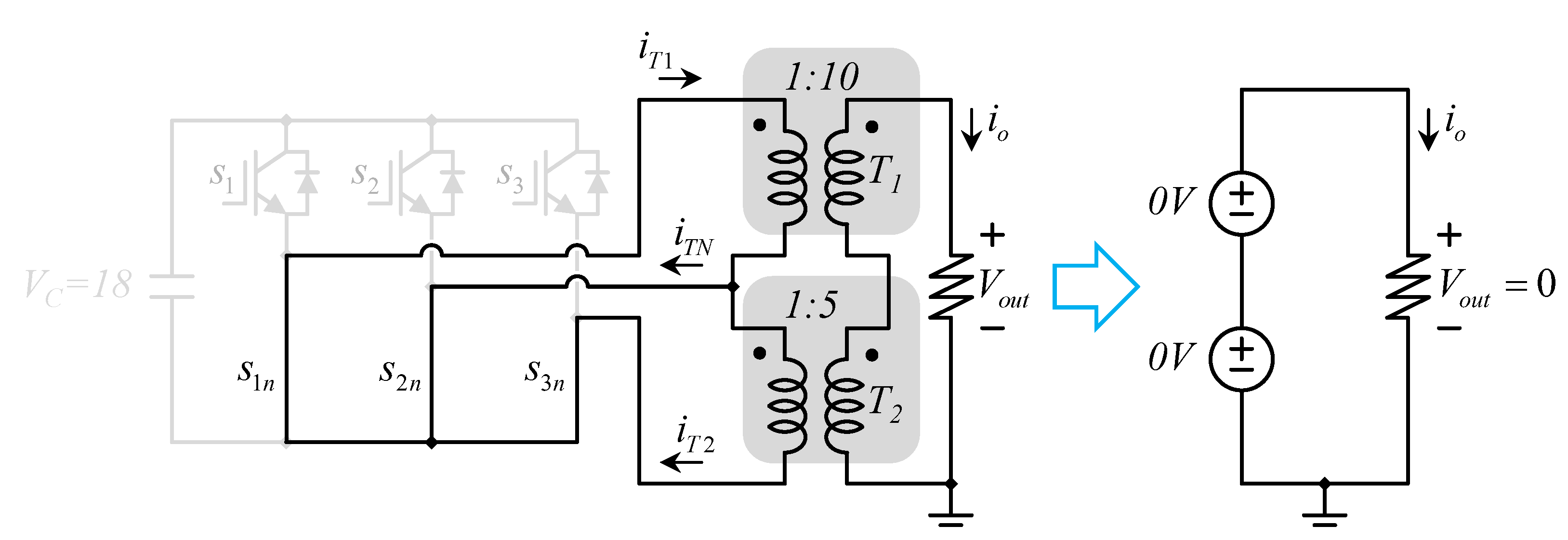
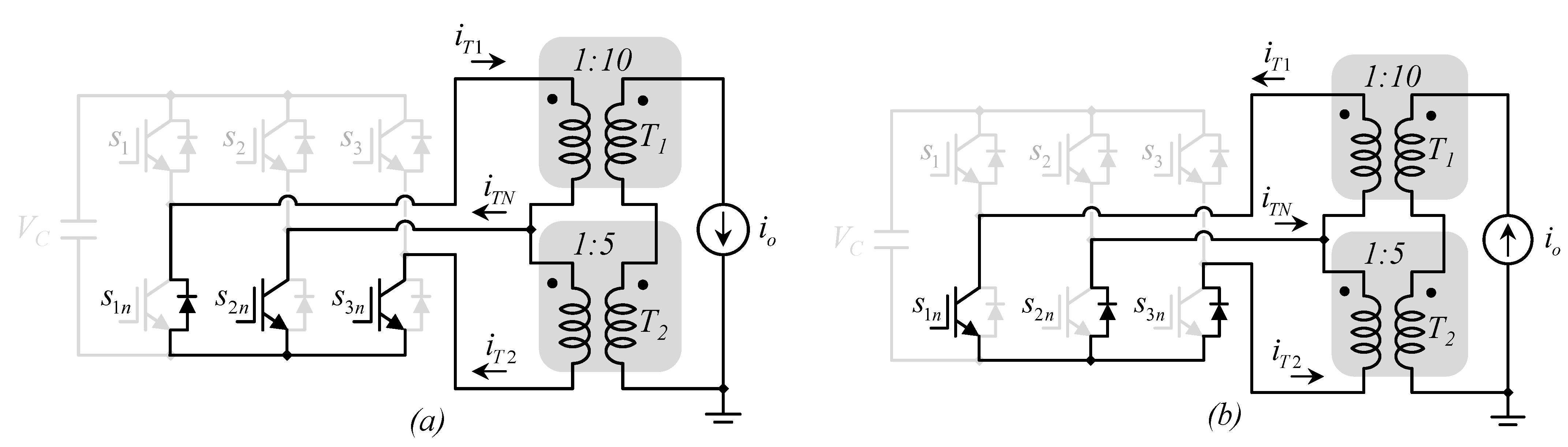
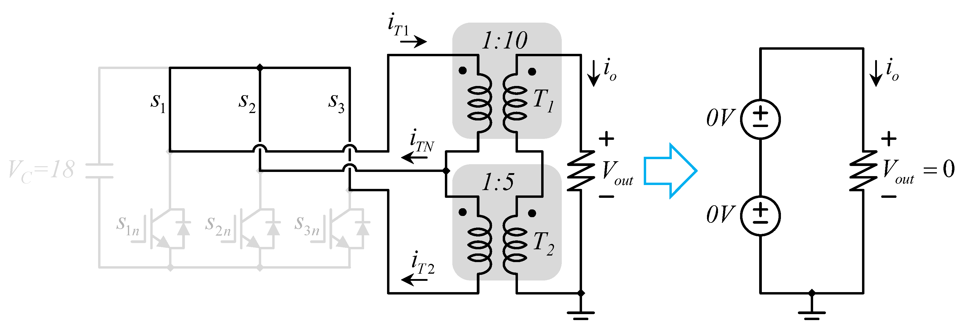
2.1. The State {0, 0, 0}

When the three firing signals are zero, the three upper switches (s1, s2, and s3) are open, and their complementary switches (s1n, s2n, and s3n) are closed, and the circuit behaves like the one shown in Figure 4. Note that the primary winding of both transistors is in a short circuit, in other words, connected to zero voltage, for which their output winding provides zero voltage to the load. In this state, the output voltage is zero.
The zero-voltage state does not mean that the load current is zero, and the output current has a path to flow in case an inductive load is connected. In this switching state, the current through transistors that are closed can be expressed in terms of the output current and the transformer’s turn ratio as in (4)–(6):
i S 1 n = i T 1 = 10 i o .
i S 3 n = i T 2 = 5 i o .
i S 2 n = i T N = i T 1 i T 2 = 5 i o .
Notice that the output current may be different from zero even if the output voltage is zero. This would depend on the load’s power factor. This state leads to zero current if the load is resistive; if the load is not resistive, it can be modeled as a current source that may have either a positive or negative direction and the converter must be prepared to deal with any current direction (this effect is due to the power factor). In case the current is positive, the current paths on the converter would look like that in Figure 5a, otherwise it would look like that in Figure 5b.
Note that depending on the load current direction, in some switches, the current flows through the transistor, and in other cases it flows through the diode.

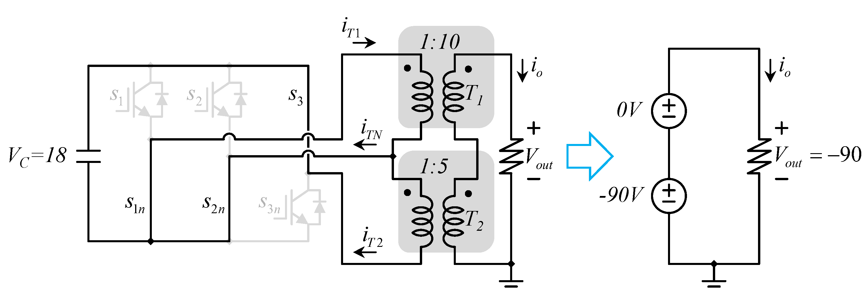
2.2. The State {0, 0, 1}

When the first two firing signals are zero and the third is one, two upper switches are open (s1 and s2) while s3 is closed. Two lower switches are closed (s1n and s2n) while the third one (s3n) is open. The circuit behaves like the one shown in Figure 6.
The primary winding of the transformer T1 is shorted (connected to zero volts), while the primary winding of the transformer T2 is connected to the input source but in a way that provides a negative voltage (the dot coincides with the negative side of the power source). In this state, the inverter provides −90 V.
In this switching state, the current through transistors that are closed can be expressed in terms of the output current and the transformer’s turn ratio as in (7)–(9):
i S 1 n = i T 1 = 10 i o .
i S 3 = i T 2 = 5 i o .
i S 2 n = i T N = i T 1 i T 2 = 5 i o .
Similar to Figure 5, Figure 7 shows the current paths for the state {0, 0, 1}.
As in the previous state, the converter must be able to operate with different output current directions to consider an operation with a power factor different than one. The load can be modeled as a current source. In case the current is positive, the current paths on the converter would look like that in Figure 7a, otherwise it would look like that in Figure 7b. Depending on the load current direction, in some switches, the current flows through the transistor, and in other cases it flows through the diode.

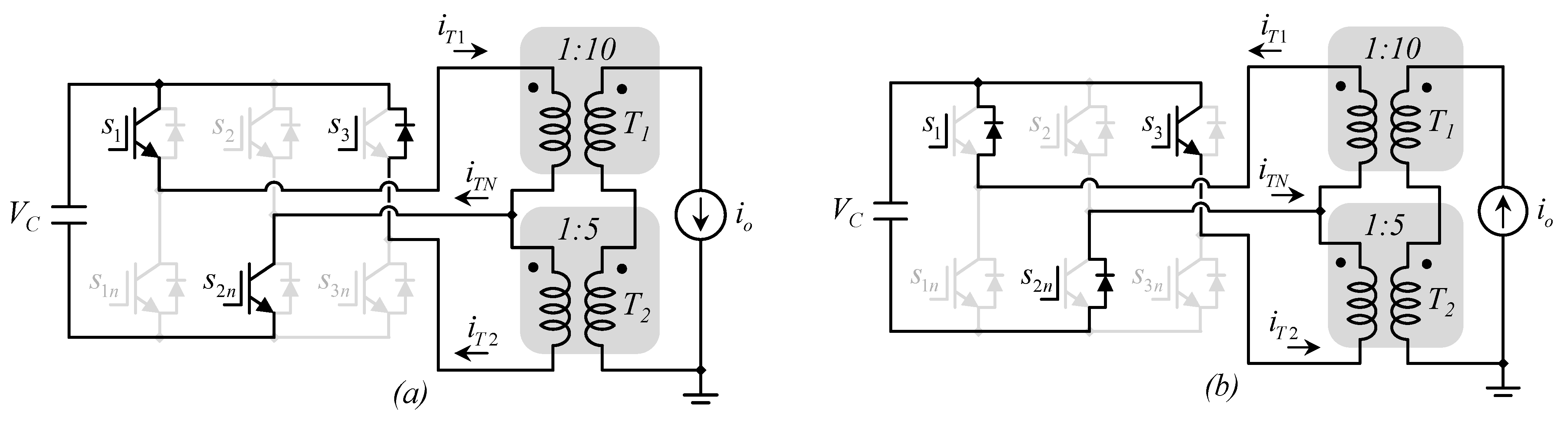
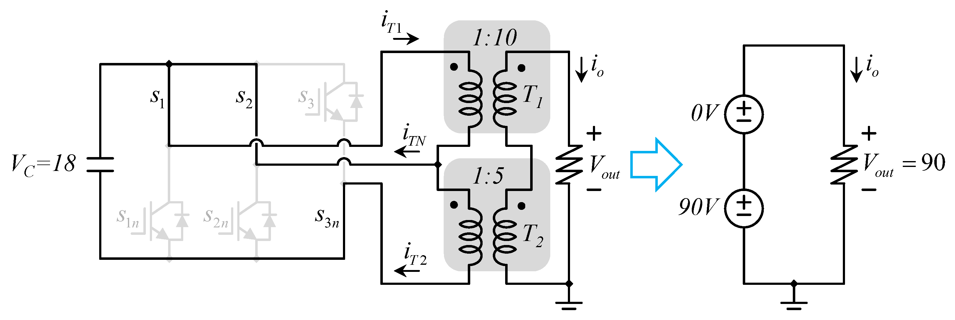
2.3. The State {0, 1, 0}

When the first and the third firing signals are zero, while the second one is one, two upper switches are open (s1 and s3) while s2 is closed. Two lower switches are closed (s1n and s3n) while the third one (s2n) is open, and the circuit behaves like in Figure 8.
The primary winding of the transformer T1 is connected to the input source, but the dot at the primary winding coincides with the negative side of the input power source and T1 provides a negative voltage (−180 V). In this state, the primary winding of the transformer T2 is connected to the input source in a positive manner (the primary dot coincides with the positive side of the input power source). In this state, the inverter provides an output of 90 V.
In this switching state, the current through transistors that are closed can be expressed in terms of the output current and the transformer’s turn ratio as in (10)–(12):
i S 1 n = i T 1 = 10 i o .
i S 3 n = i T 2 = 5 i o .
i S 2 = i T N = i T 1 i T 2 = 5 i o .
As in previous states, the converter must be able to operate with different output current directions to consider an operation with a power factor different than one. The load can be modeled as a current source. In case the current is positive, the current paths on the converter would look like that in Figure 9a, otherwise it would look like that in Figure 9b. Depending on the load current direction, in some switches, the current flows through the transistor, and in other cases it flows through the diode.

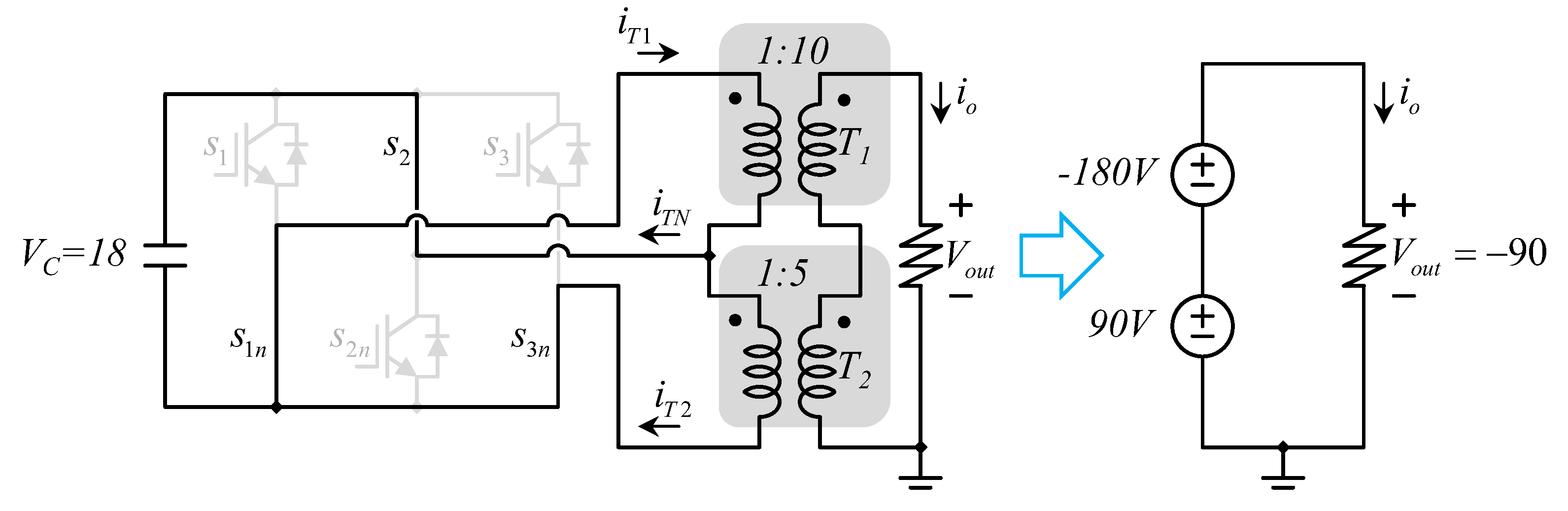
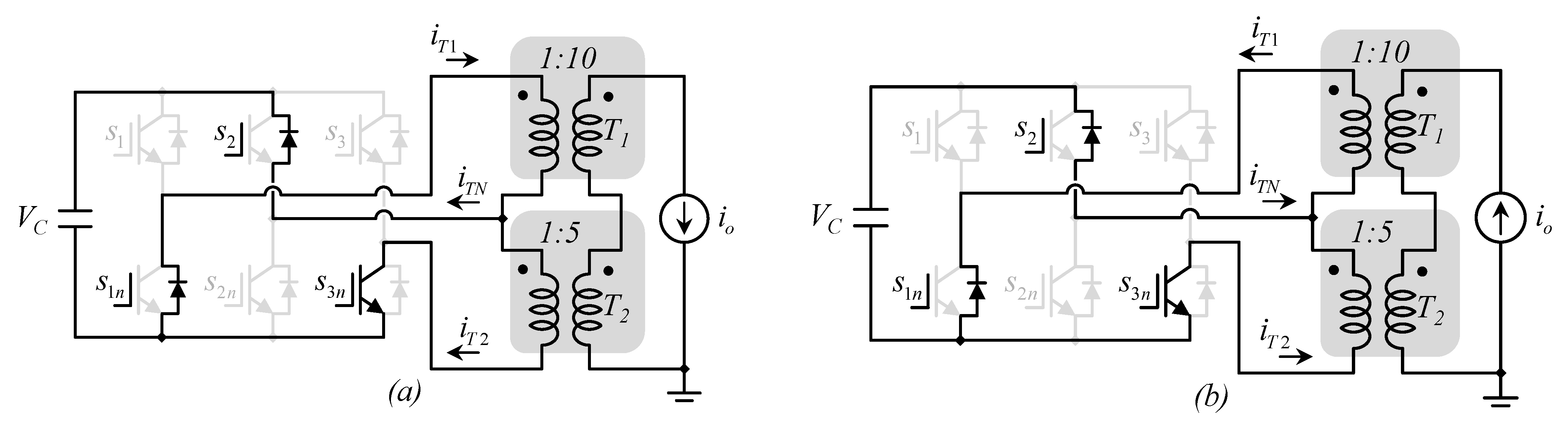
2.4. The State {0, 1, 1}

When the first firing signal is zero, while the second and third are one, the first upper switch (s1) is open, while the other two (s2 and s3) are closed. The first lower switch (s1n) is closed, while the other two (s2n and s3n) are open. In this state the circuit behaves like in Figure 10.
The primary winding of the transformer T1 is connected to the input source, but the dot at the primary winding coincides with the negative side of the input power source and T1 provides a negative voltage (−180 V). The primary winding of the transformer T2 is shorted or connected to zero volts (it is not contributing to the output voltage in this switching state). In this state, the inverter provides an output of −180 V.
In this switching state, the current through transistors that are closed can be expressed in terms of the output current and the transformer’s turn ratio as in (13)–(15):
i S 1 n = i T 1 = 10 i o .
i S 3 = i T 2 = 5 i o .
i S 2 = i T N = i T 1 i T 2 = 5 i o .
As in previous states, the converter must be able to operate with different output current directions to consider an operation with a power factor different than one. The load can be modeled as a current source. In case the current is positive, the current paths on the converter would look like that in Figure 11a, otherwise it would look like that in Figure 11b. Depending on the load current direction, in some switches, the current flows through the transistor, and in other cases it flows through the diode.

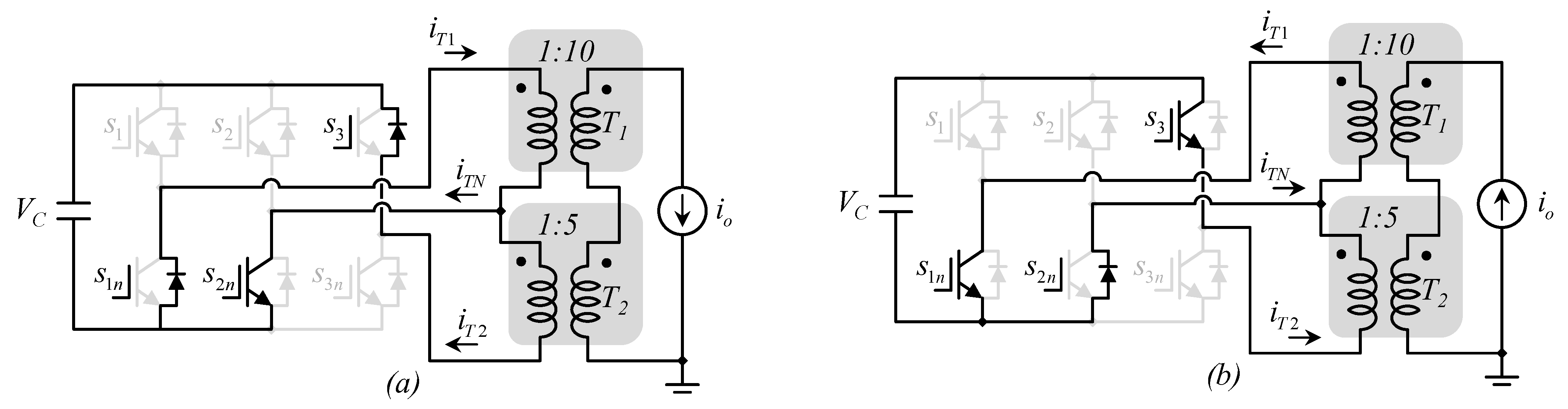
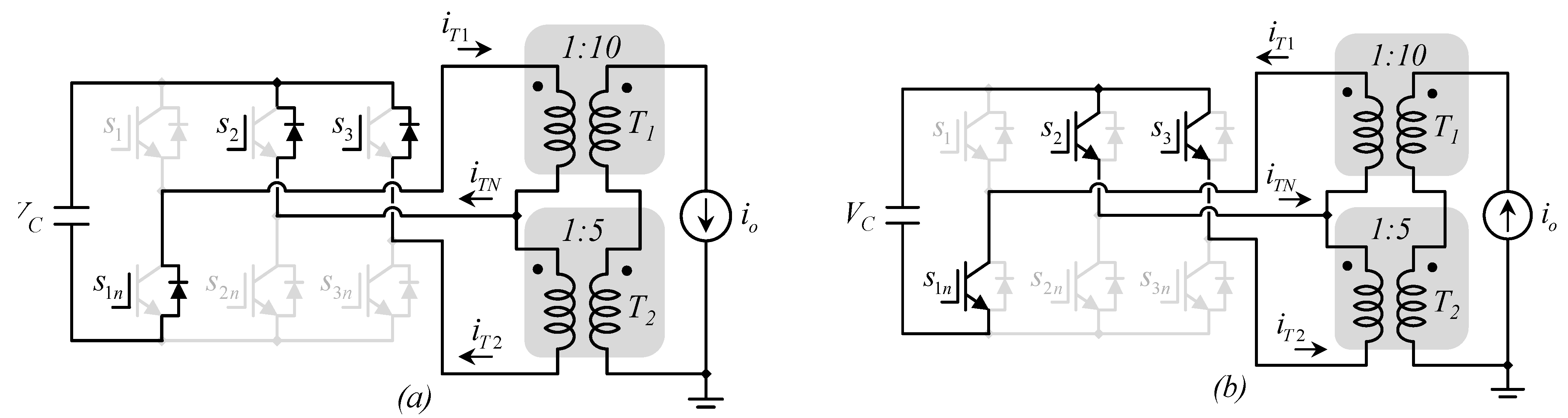
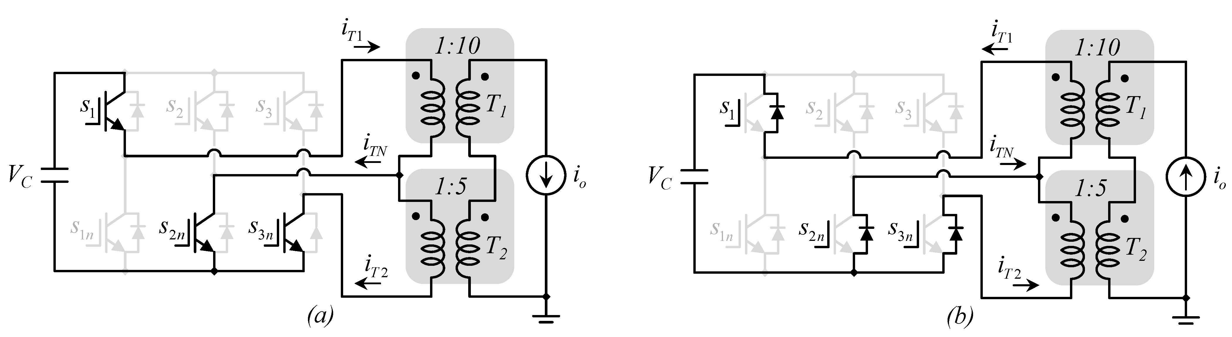
2.5. The State {1, 0, 0}

When the first firing signal is one, while the second and third are zero, the first upper switch (s1) is closed and the other two (s2 and s3) are open. The first lower switch (s1n) is open, while the other two (s2n and s3n) are closed. In this state, the circuit behaves like in Figure 12.
The primary winding of the transformer T1 is connected to the input source, in a positive manner (the dot is connected to the positive side of the input power source), then it provides 180 V to the output. The primary winding of the transformer T2 is shorted or connected to zero volts (it is not contributing to the output voltage in this switching state). In this state, the inverter provides an output of 180 V.
In this switching state, the current through transistors that are closed can be expressed in terms of the output current and the transformer’s turn ratio as in (16)–(18):
i S 1 = i T 1 = 10 i o .
i S 3 n = i T 2 = 5 i o .
i S 2 n = i T N = i T 1 i T 2 = 5 i o .
As in previous states, the converter must be able to operate with different output current directions to consider an operation with a power factor different than one. The load can be modeled as a current source. In case the current is positive, the current paths on the converter would look like that in Figure 13a, otherwise it would look like that in Figure 13b. Depending on the load current direction, in some switches, the current flows through the transistor, and in other cases it flows through the diode.

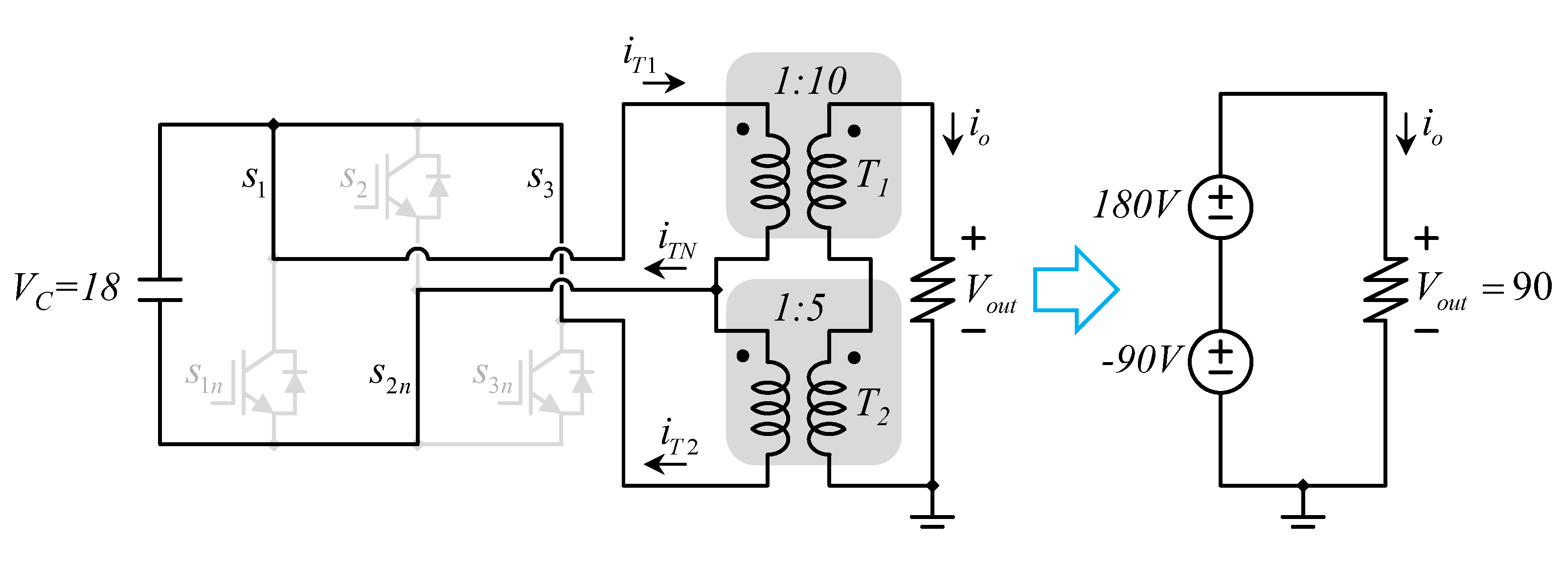
2.6. The State {1, 0, 1}

When the first and the third firing signals are one, while the second signal is zero, the first and the third upper switches (s1 and s3) are closed while the second upper switch (s2) is open. The first and the third lower switches (s1n, and s3n) are open, while the other switch (s2n) is closed. In this state, the circuit behaves like in Figure 14.
The primary winding of the transformer T1 is connected to the input source, in a positive manner (the dot is connected to the positive side of the input power source), then it provides 180 V to the output. The primary winding of the transformer T2 is also connected to the input power source, but in a negative manner (the dot coincides with the negative side of the power source), and in this case, T2 contributes with −90 V to the load. In this state, the inverter provides an output of 90 V.
In this switching state, the current through transistors that are closed can be expressed in terms of the output current and the transformer’s turn ratio as in (19)–(21):
i S 1 = i T 1 = 10 i o .
i S 3 = i T 2 = 5 i o .
i S 2 n = i T N = i T 1 i T 2 = 5 i o .
As in previous states, the converter must be able to operate with different output current directions to consider an operation with a power factor different than one. The load can be modeled as a current source. In case the current is positive, the current paths on the converter would look like that in Figure 15a, otherwise it would look like that in Figure 15b. Depending on the load current direction, in some switches, the current flows through the transistor, and in other cases it flows through the diode.

2.7. The State {1, 1, 0}

When the first two firing signals are one, while the last one is zero, the first and the second upper switches (s1 and s2) are closed while the third upper switch (s3) is open. The first and the second lower switches (s1n and s2n) are open, while the last one (s3n) is closed. In this state, the circuit behaves like in Figure 16.
The primary winding of the transformer T1 is shorted and provides no voltage to the output side. The primary winding of the transformer T2 is connected to the input power source in a positive manner (the dot coincides with the positive side), and in this case, T2 contributes with 90 V to the load. In this state, the inverter provides an output of 90 V.
In this switching state, the current through transistors that are closed can be expressed in terms of the output current and the transformer’s turn ratio as in (22)–(24):
i S 1 = i T 1 = 10 i o .
i S 3 n = i T 2 = 5 i o .
i S 2 = i T N = i T 1 i T 2 = 5 i o .
As in previous states, the converter must be able to operate with different output current directions to consider an operation with a power factor different than one. The load can be modeled as a current source. In case the current is positive, the current paths on the converter would look like that in Figure 17a, otherwise it would look like that in Figure 17b. Depending on the load current direction, in some switches, the current flows through the transistor, and in other cases it flows through the diode.

2.8. The State {1, 1, 1}

When all firing signals are one, all upper switches (s1, s2, and s3) are closed while all lower switches (s1n, s2n, and s3n) are open. In this state, the circuit behaves like in Figure 18.
Both transformers’ primary windings are shorted and provide no voltage to the output side. In this state, the inverter provides an output of 0 V.
In this switching state, the current through transistors that are closed can be expressed in terms of the output current and the transformer’s turn ratio as in (25)–(27):
i S 1 = i T 1 = 10 i o .
i S 3 = i T 2 = 5 i o .
i S 2 = i T N = i T 1 i T 2 = 5 i o .
As in previous states, the converter must be able to operate with different output current directions to consider an operation with a power factor different than one. The load can be modeled as a current source. In case the current is positive, the current paths on the converter would look like that in Figure 19a, otherwise it would look like that in Figure 19b. Depending on the load current direction, in some switches, the current flows through the transistor, and in other cases it flows through the diode.

2.9. Summary of the Converter’s Equivalent Circuits

Table 1 shows a summary in which firing signals are shown with their respective output voltage.
Table 1 also includes the information about the contribution of transformers, whether it is positive, negative, or zero. The last column indicates the output voltage considering that the turn ratio of transformer T1 is 1:10, the turn ratio of transformer T2 is 1:5, and the input voltage (the capacitor’s voltage) is 18 V.
We can see from the analysis that the converter has eight equivalent circuits, but only five different output voltage levels, since two pairs of states are redundant, which means they provide the same voltage. In this case, the states {0, 0, 1} and {0, 1, 0} both provide −90 V, and the states {1, 0, 1} and {1, 1, 0} both provide 90 V.
Evidently, the designer can choose some parameters, such as the turn ratio of transformers, and the input voltage may be different, but the converter can provide five different output voltage levels, which can produce a five-level stepped waveform.
The operation of the inverter requires the appropriate selection of switching functions. To operate the dc-ac inverter, we chose only the switching states marked in bold in Table 1.
Figure 20 shows important signals of the converter. From top to bottom, the first three signals are the selected switching functions and they are directly applied to the three upper switches (s1, s2, and s3), while lower switches (s1n, s2n, and s3n) have the opposite (complementary) logic signals.
Figure 20 also shows the output voltage (Vout), the ideal sinusoidal waveform is shown in light gray, and the real stepped waveform is shown in black, and this is the multilevel waveform, with five levels. Finally, Figure 20 also shows the voltage at the secondary winding (output) of both transformers (T1 and T2). VT1 (180 V peak) has twice the peak amplitude of VT1 (90 V peak).
The output voltage can be expressed as the summation of the voltage at both transformers’ secondary windings, as in (28):
V o u t = V T 1 + V T 2 ;
From the theoretical signals, we can also observe that four of the six transistors switch at the output frequency (i.e., 60 Hz), while two of them switch at three times the output frequency (i.e., 180 Hz); still, the switching frequency is relatively low for the capacity of a regular IGBT or a MOSFET.
The full-bridge power stage operates with a dead-time among the upper and lower transistors of the same phase, and this may cause a small distortion on the output current of a traditional PWM inverter, as described in [20]. In this case, since the switching frequency is low, the dead-time is negligible compared to the time in which transistors were on, and no effect was observed. However, if PWM is used, a dead-time elimination method (such as the one described in [20]) may be used to eliminate any current distortion.

2.10. Dynamical Model of the System

The elements that store energy in the system shown in Figure 3 are basically the inductor and capacitor of the boost converter, and despite that transformers have some stored energy in their magnetizing inductance, the amount of stored energy is relatively small. A simple mathematical model can be derived by analyzing the boost converter and then adding the input current of the six-pack module as the output current of the boost converter in the capacitor.
Figure 21 shows the boost converter with a current source as a load, and the load current ix is the input current to the six-pack module, as shown in Figure 3.
From the equivalent circuits, it is possible to use the standard averaging technique to describe the dynamics of the state variables. In this case, the state variables are the current through the inductor and the voltage across the capacitor [21]. The average voltage across the inductor and the average current through the capacitor would be expressed as in (29) and (30), respectively:
L d i L d t = d v g + 1 d v g v C .
C d v C d t = d i x + 1 d i L i x .
where d is the duty cycle of the switch sa; in other words, the time in each switching cycle that the converter behaves like the circuit in Figure 21b, divided over the switching period.
Equations (29) and (30) can be simplified and rewritten as Equations (31) and (32):
L 1 d i L 1 d t = d v g 1 d v C 1 .
C 1 d v C 1 d t = 1 d i L 1 i x .
From the dynamic Equations (31) and (32), the steady-state (or equilibrium) operation can be calculated. In a steady state, the derivative of state variables is zero, and then, making the derivatives in (31) and (32) equal to zero, the voltage in C1 can be expressed as in (33) and the current through the inductor can be expressed as in (34):
V C = 1 1 D V g .
I L 2 = 1 1 D I x .
Upper case letters are used in (33) and (34) to indicate steady-state values or variables in the equilibrium condition.

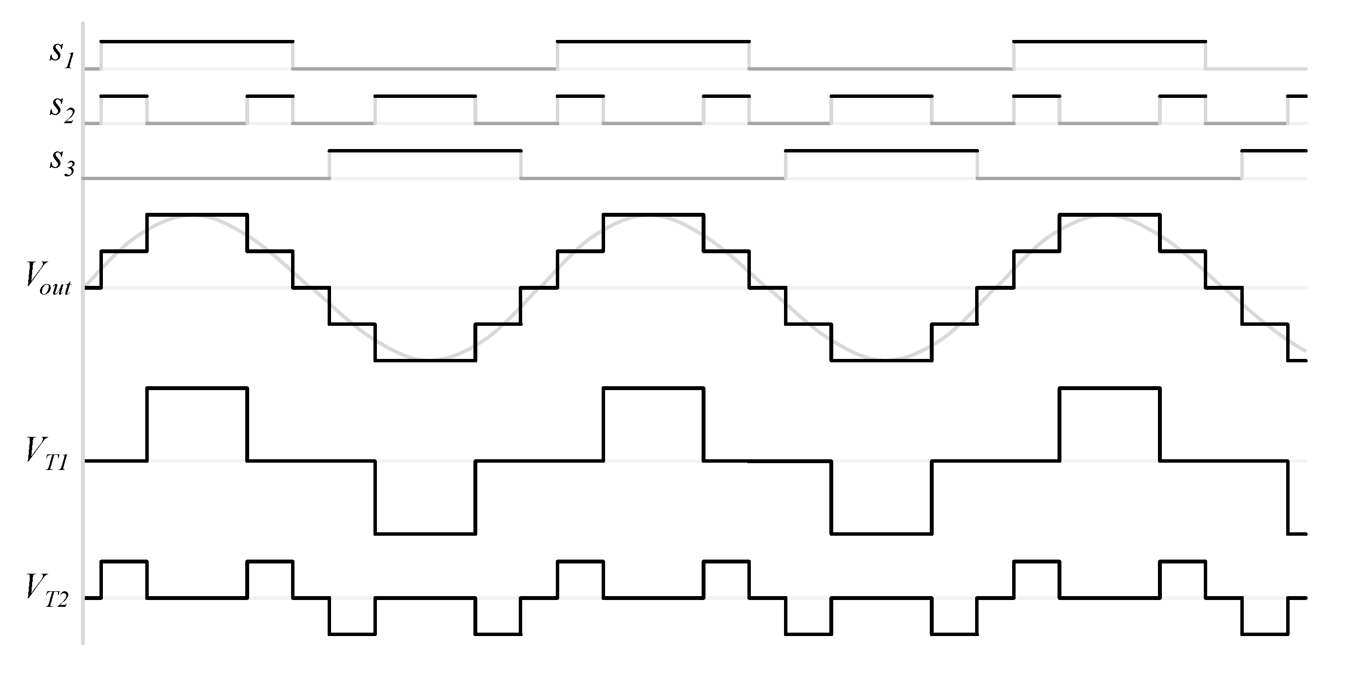
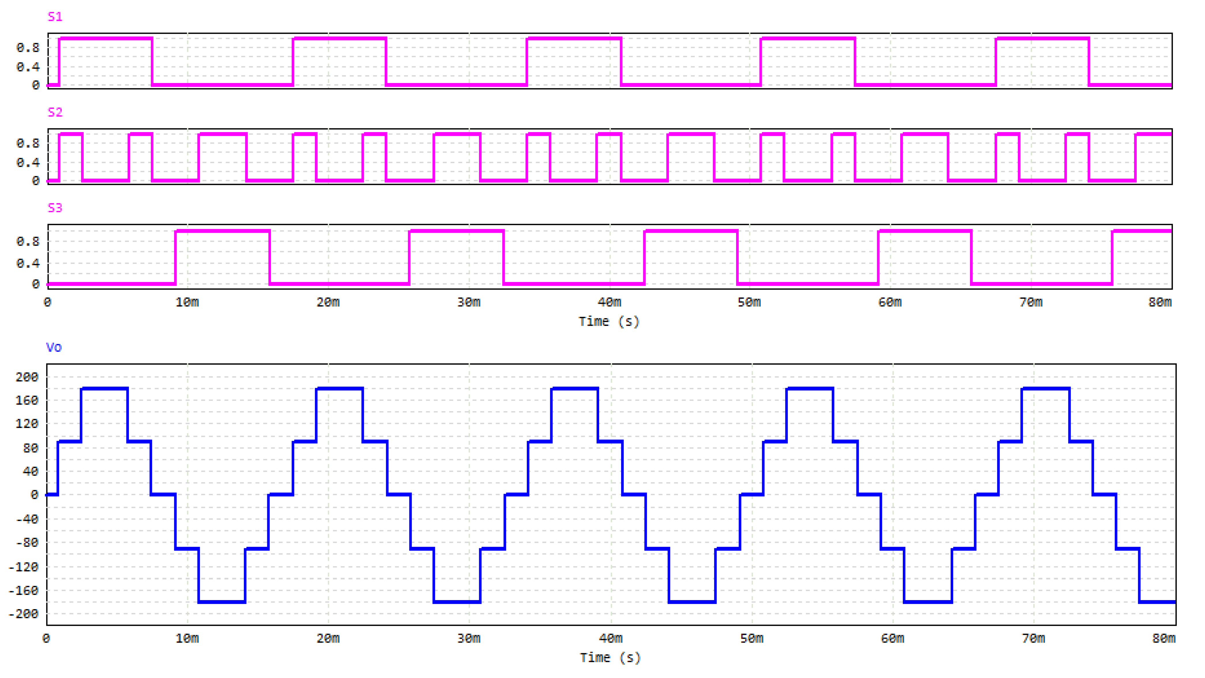
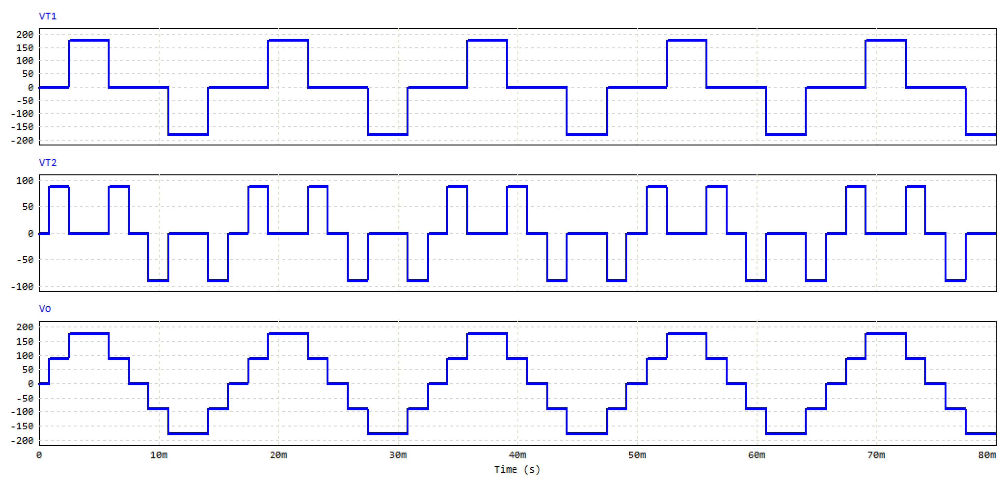
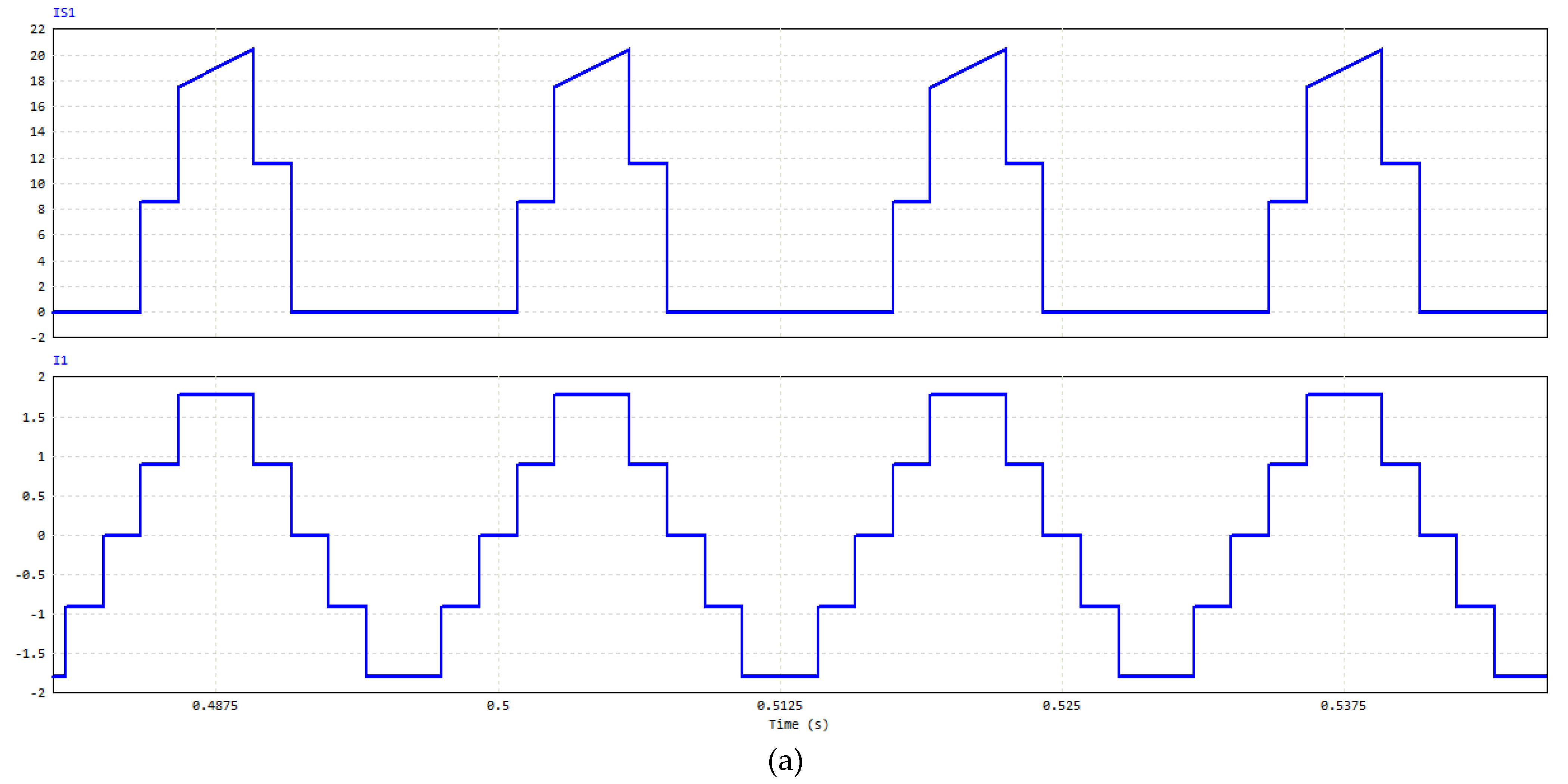
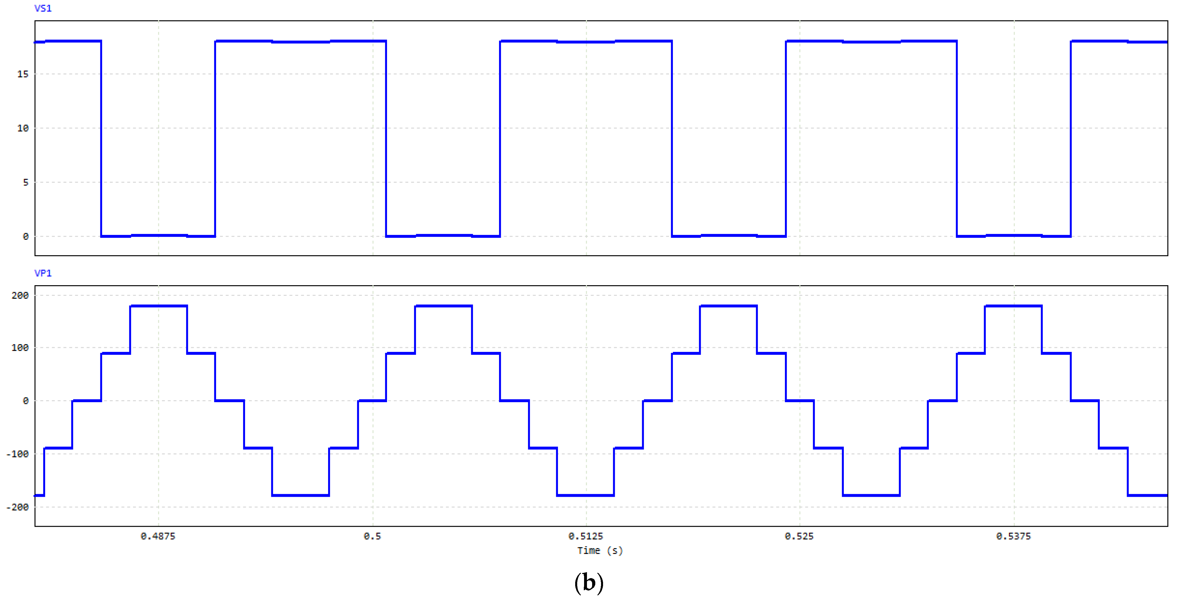
3. Demonstrative Results

To corroborate the operation of the proposed converter, the converter was simulated in the software PSIM (2022-1) using a computer with an Intel i7 processor (11th Gen i7-1165G7 at 2.80 GHz), 32 GB of Ram memory, and Windows 11 Pro (64 bits). The simulation parameters are shown in Table 2.
Several tests were performed with and without magnetizing inductance (in parallel with the transformers’ primary winding), and the difference was too small to be observed on the waveforms and only an increase of 0.05% on the THD was measured.
Figure 22 shows the simulation schematics, whereby the customizable power semiconductor element was used to simulate the transistors. All transistors have an antiparallel diode, which is a characteristic of the six-pack. The input voltage is 12 V, and the transformers’ turn ratios are also the same as in the analysis (1:10 for T1 and 1:5 for T2).
The simulator requires to have a reference (ground) in floating elements of the circuits, but in the application, the input side and the output side of transformers are naturally electrically isolated.
Figure 23 shows the switching signals (up) along with the output voltage, Vout. The voltage is consistent with what we expected, and with the waveform shown in Figure 20. The simulation shows that the proposed topology can make the voltage conversion from the dc input to the five-level output.
The converter was used to generate a 60 Hz multilevel voltage output with a peak amplitude of 180 V (see Table 1). Figure 24 shows the voltage at transformers’ secondary winding along with the output voltage, which is the sum of both transformers’ output voltages. The measured total harmonic distortion (THD) of the staircase output voltage waveform generated by the converter was around 20%, although it can be improved by adding an output filter, increasing the number of levels, or implementing a PWM modulation.
We have also included important waveforms for the semiconductors of the power converter, as can be observed in Figure 25, where the current through and voltage across the switch S1 are compared to the current and voltage at the output, respectively.
It can be seen that the peak values of current and voltage in semiconductors correspond to the input current and voltage values. It is also important to notice that, as is expected in multilevel converters, the semiconductors only block a portion of the output voltage, which allows the selection of components with smaller voltage ratings.
The simulations were performed considering some parasitic components in the transformer, however the addition of non-idealities such as magnetizing and leakage inductance will not drastically affect the performance of the converter. For instance, these inductances could cause a small distortion in the levels of the converter that can be compensated by increasing the dc bus capacitance. The simulation was performed in a specialized software which considers non-ideal models for semiconductors and other elements, and it showed that the converter can perform the proposed conversion and demonstrated that the inverter can be built with a six-pack IGBT module.

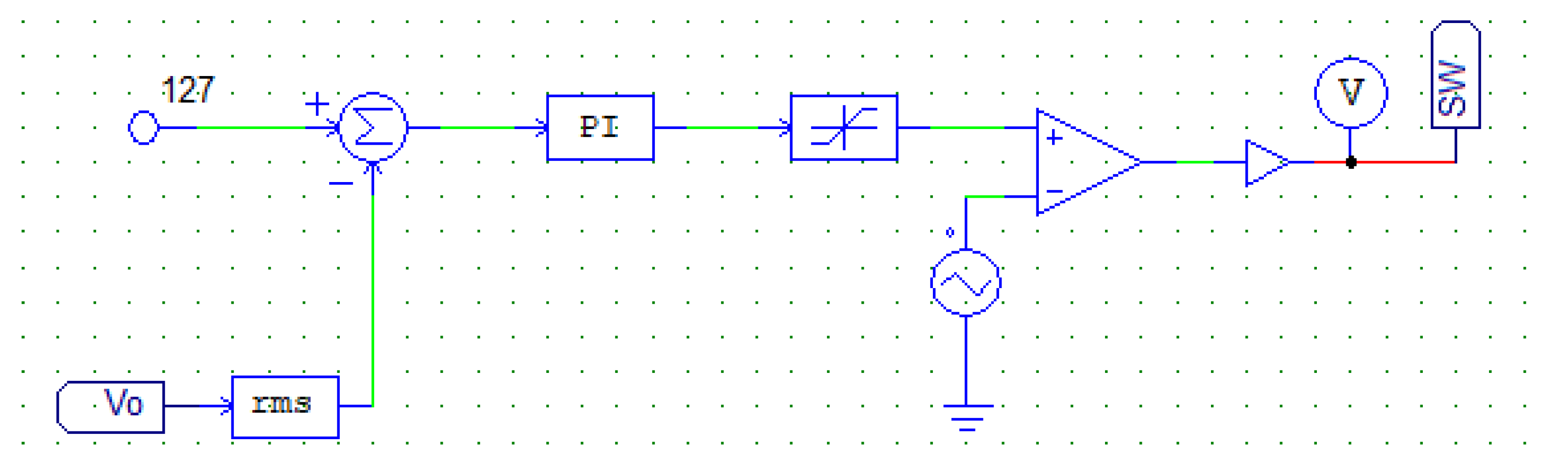
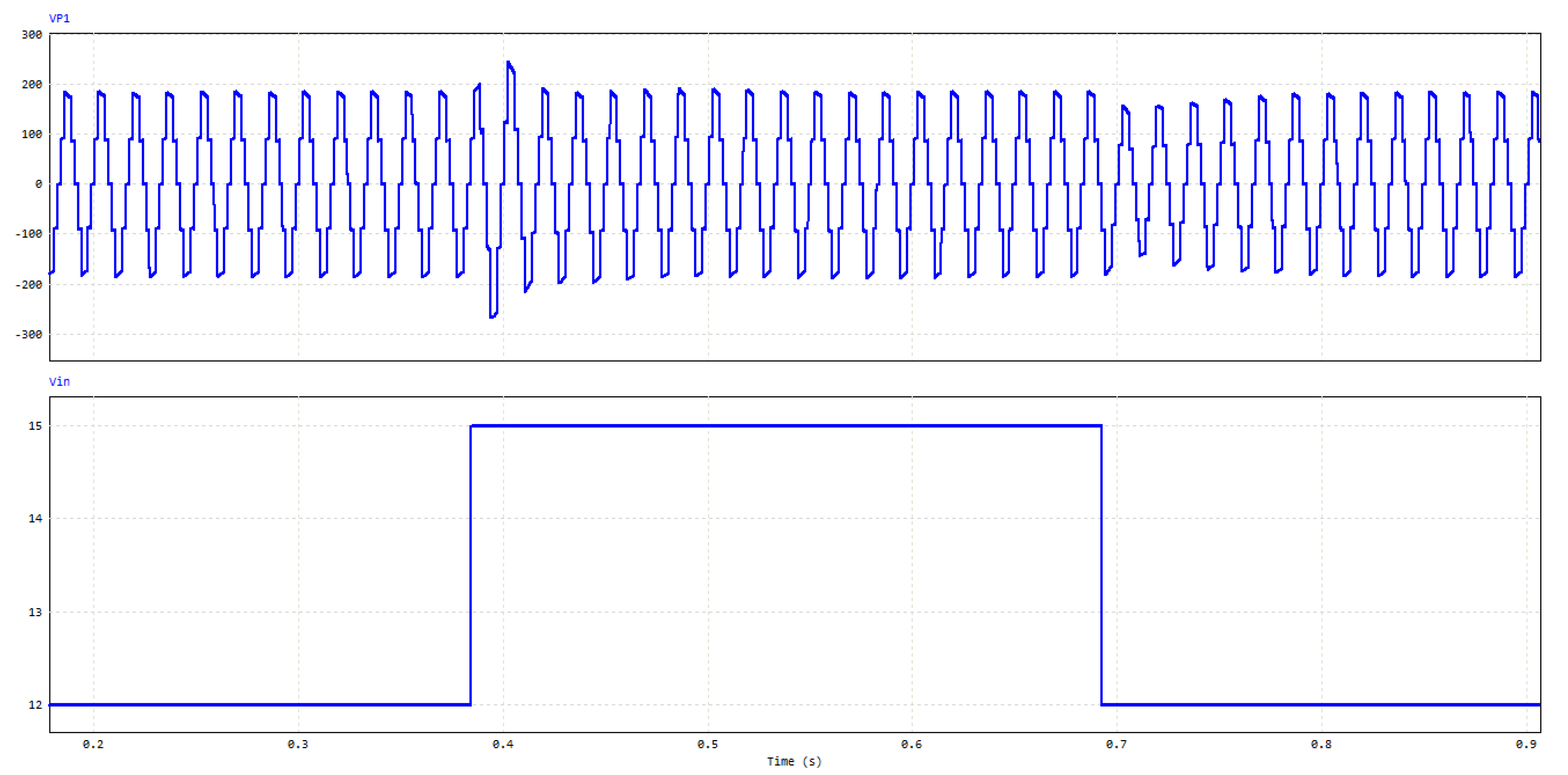
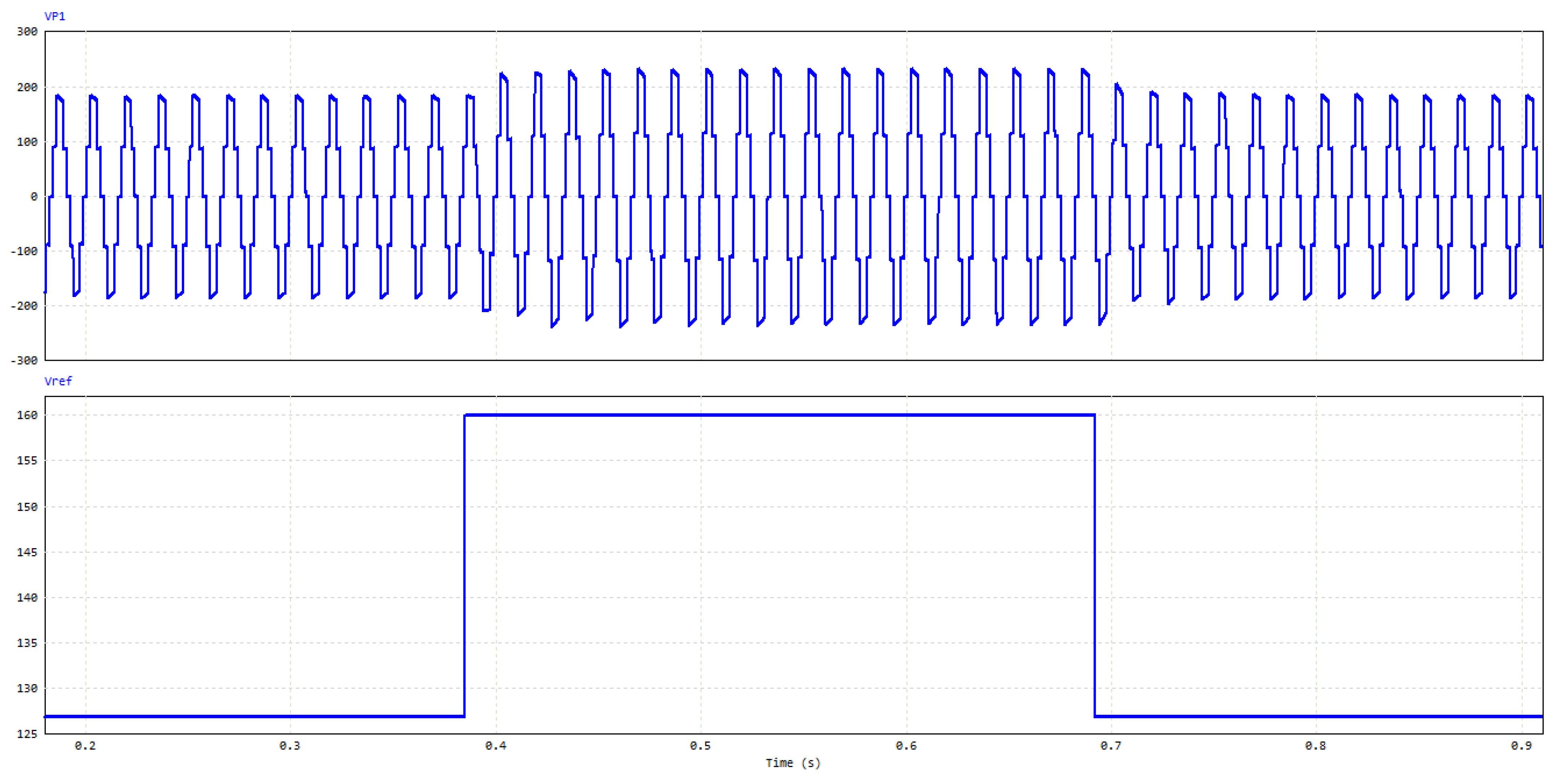
Operation of the Converter under Closed-Loop Control
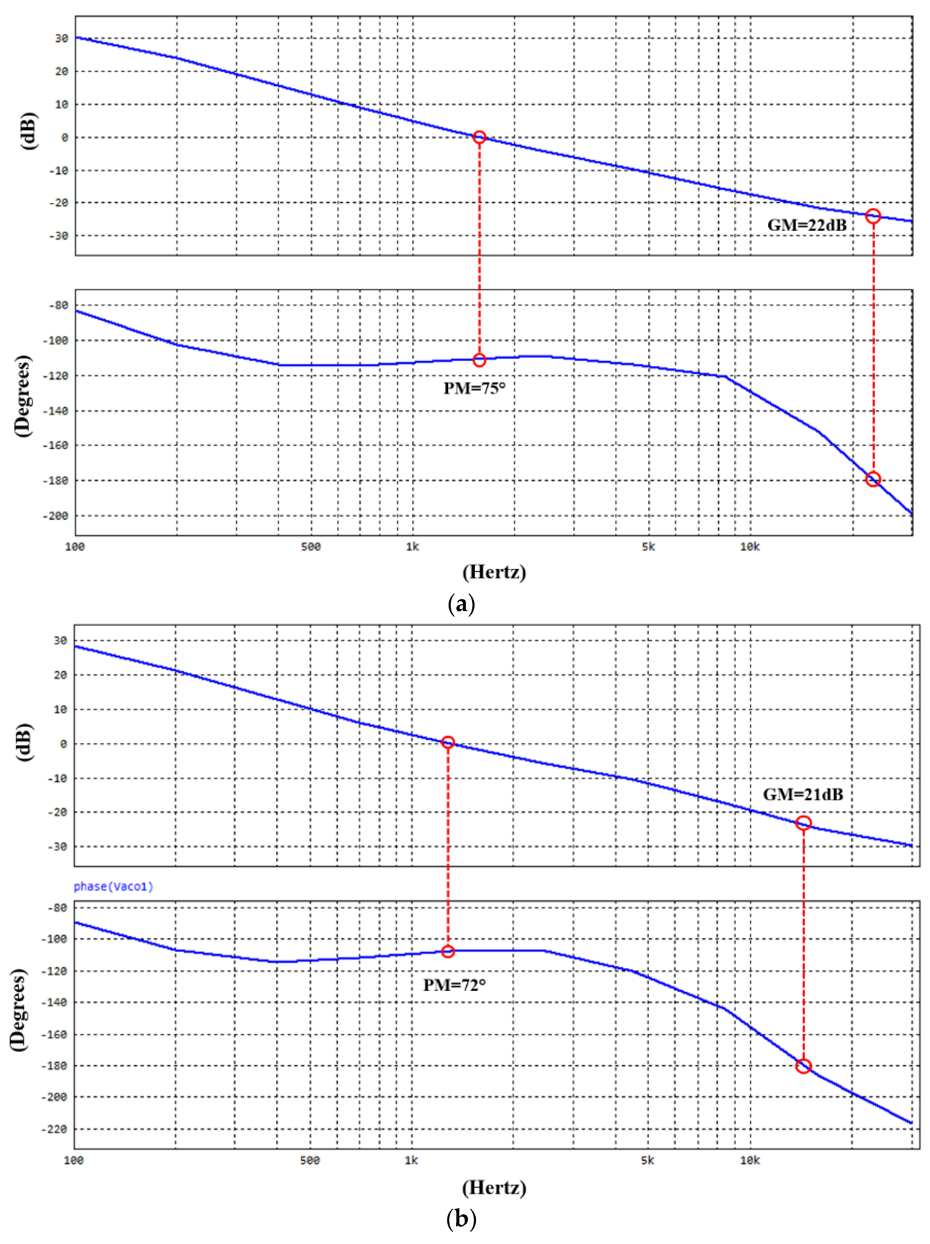
Due to the nature of the output voltage waveform created by the proposed topology (staircase), which has the aforementioned advantages of low-frequency switching and low losses, the direct regulation of the output voltage is not permitted. However, the closed-loop operation of the converter is possible by including PWM modulation or by implementing a dc pre-regulator.
In this work, we chose to explore the option of the dc pre-regulator stage to demonstrate the regulation capability. It is worth noting that in most applications, this pre-regulator is required, for instance in PV grid-tied inverters and motor drivers.
The designed control scheme consists of a traditional PI controller which regulates the RMS value of the output voltage, by controlling the operation of the dc pre-regulator, as can be seen in Figure 26. The controller was tuned considering that the dc bus bulk capacitor presents slow dynamics. There exist multiple options for designing the control stage, however here we only show an alternative to demonstrate the application of the proposed topology if the closed-loop operation is required.
The RMS value in Figure 26 was calculated with the moving average or window strategy to ensure a precise measurement.
We performed two different tests to corroborate the performance of the converter under closed-loop operation. The first test was for changes at the input source. We changed the input voltage from the nominal 12 to 15 V and back, and from 12 to 9 V and vice versa, and the setpoint for the output voltage was fixed to 127 VRMS. As can be seen in Figure 27, the output reaches its steady-state value after some milliseconds of the input voltage change. It can be seen that the output voltage is stably bounded and correctly regulated in spite of the abrupt input voltage changes.
The second test consisted in changing the output voltage setpoint reference of the converter while keeping the input voltage constant. The reference was changed from 127 to 160 VRMS and back, and from 127 to 100 VRMS and vice versa. The results of this test can be seen in Figure 28. As can be observed, the output voltage followed the reference after a short transient of a few milliseconds, and it is worth mentioning that although the changes in the reference were suddenly made, the converter followed the control commands properly.
To verify the stability margins of the closed-loop controller, we included the bode plots for the closed-loop system. The bode diagrams were obtained directly from the simulation by perturbing the reference signal with a frequency-varying sinusoidal waveform of around 10% of the nominal value of the reference. In Figure 29, we included the bode plots of two tests to characterize the effect of the output transformer in the closed-loop operation of the system. It can be seen from the plots that the closed-loop system presents a sufficient phase margin of around 70° which, alongside with the gain margin of around 20 dB, guarantees a stable operation of the converter. It can be noticed that the addition of the output transformer slightly decreases the crossover frequency (bandwidth) of the closed-loop system but does not have a substantial impact on the stability of the converter.

4. Discussion

The proposed topology can be built with a six-pack transistors module, which is an advantage from the manufacturing point of view. Six-pack transistors modules are widely used in many applications, and they are available in a wide range of voltages, currents, power dissipation, and with several types of devices, such as MOSFETs, IGBTs, etc. They are off-the-shelf devices.
Four of the six transistors switched at the output frequency (60 Hz), while the other two switched at three times the switching frequency (180 Hz). However, three times the switching frequency is still considered a low frequency for IGBTs and MOSFETS.
The main disadvantage of the proposed topology is that it requires two transformers, but their turn ratios can be used as an extra degree of freedom during the design, to customize the voltage gain according to the application. Furthermore, if one transformer is chosen with a 1:1 turn ratio, and no isolation is required, the transformers can be omitted while the converter performs the same application.
Compared to other topologies, the proposed one has a low-voltage stress on transistors; on the other hand, the current may be relatively large since it is proportional to the output current multiplied by the turn ratios of transformers. This makes the converter more suitable to be used for MOSFETs, whereby the on-resistance may help to reduce the conduction losses compared to other topologies.

5. Conclusions

This article introduced a single-phase five-level multilevel inverter topology which is based on a three-phase arrangement of transistors (what we usually call a six-pack module) and two transformers. The proposed converter requires a single dc input source, and the input source may have low amplitude since the turn ratio of transformers can be used to boost the voltage. Six-pack transistors modules are commercially available (off-the-shelves), and since those packages are widely used to build low-power three-phase inverters, their use simplifies the manufacturing process. The converter has low-voltage stress on transistors. Their main drawback is the use of two transformers, but those transformers allow using the same topology for several input voltage levels by changing the transformers’ turn ratios. To verify the operation of the proposed multilevel inverter, a computer-based simulation was performed with the specialized software PSIM, a software that considers parasitic components (non-ideal). The results show that the proposed converter can work properly and perform the power conversion as expected.

Author Contributions

J.C.R.-C. and F.A.G.-S. contributed to the conceptualization of the article; J.E.V.-R. and J.C.M.-M. contributed to the methodology; A.V.-G. contributed to the software, validation, and formal analysis; H.R.R.-C. and J.C.R.-C. wrote the draft and prepared the manuscript. All authors have read and agreed to the published version of the manuscript.

Funding

The authors would like to thank Universidad Panamericana, for their support through the program “Fomento a la Investigación UP 2022”, and project “Estudio de topologías de convertidores de cd-cd” UP-CI-2022-GDL-06-ING.

Data Availability Statement

Not applicable.

Acknowledgments

The authors would like to thank CERREY S.A. de C.V., Universidad Panamericana, The University of Sheffield, and Tecnológico de Monterrey.

Conflicts of Interest

The authors declare no conflict of interest.

References

  1. Kouro, S.; Malinowski, M.; Gopakumar, K.; Pou, J.; Franquelo, L.G.; Wu, B.; Rodriguez, J.; Perez, M.A.; Leon, J.I. Recent advances and industrial applications of multilevel converters. IEEE Trans. Ind. Electron. 2010, 57, 2553–2580. [Google Scholar] [CrossRef]
  2. Rodriguez, J.; Lai, J.S.; Peng, F.Z. Multilevel inverters: A survey of topologies, control and applications. IEEE Trans. Ind. Electron. 2002, 49, 724–738. [Google Scholar] [CrossRef] [Green Version]
  3. Bughneda, A.; Salem, M.; Richelli, A.; Ishak, D.; Alatai, S. Review of Multilevel Inverters for PV Energy System Applications. Energies 2021, 14, 1585. [Google Scholar] [CrossRef]
  4. Alotaibi, S.; Darwish, A. Modular Multilevel Converters for Large-Scale Grid-Connected Photovoltaic Systems: A Review. Energies 2021, 14, 6213. [Google Scholar] [CrossRef]
  5. Choudhury, S.; Bajaj, M.; Dash, T.; Kamel, S.; Jurado, F. Multilevel Inverter: A Survey on Classical and Advanced Topologies, Control Schemes, Applications to Power System and Future Prospects. Energies 2021, 14, 5773. [Google Scholar] [CrossRef]
  6. Zhang, F.; Peng, F.Z.; Qian, Z. Study of the multilevel converters in DC-DC applications. In Proceedings of the 2004 IEEE 35th Annual Power Electronics Specialists Conference, Aachen, Germany, 20–25 June 2004; Volume 2, pp. 1702–1706. [Google Scholar]
  7. Peng, F.Z. A generalized multilevel inverter topology with self voltage balancing. IEEE Trans. Ind. Appl. 2001, 37, 611–618. [Google Scholar] [CrossRef]
  8. Lai, J.-S.; Peng, F.Z. Multilevel converters-a new breed of power converters. IEEE Trans. Ind. Appl. 1996, 32, 509–517. [Google Scholar]
  9. Nabae, A.; Takahashi, I.; Akagi, H. A new neutral-point-clamped PWM inverter. IEEE Trans. Ind. Appl. 1981, IA-17, 518–523. [Google Scholar] [CrossRef]
  10. Chen, G.; Yang, J. A Modified Modulation Strategy for an Active Neutral-Point-Clamped Five-Level Converter in a 1500 V PV System. Electronics 2022, 11, 2289. [Google Scholar] [CrossRef]
  11. Li, W.-J.; Li, D.-S.; Zhang, J.-W. Model-Based Design and Experimental Validation of Control System for a Three-Level Inverter. Electronics 2022, 11, 1979. [Google Scholar] [CrossRef]
  12. Meynard, T.A.; Foch, H. Multi-Level Choppers for High Voltage Applications. EPE J. 1992, 2, 45–50. [Google Scholar] [CrossRef]
  13. Hochgraf, C.; Lasseter, R.; Divan, D.; Lipo, T.A. Comparison of multilevel inverters for static var compensation. In Proceedings of the 1994 IEEE Industry Applications Society Annual Meeting, Denver, CO, USA, 2–6 October 1994; pp. 921–928. [Google Scholar]
  14. Marquardt, R. Modular multilevel converter: An universal concept for HVDC-networks and extended DC-bus-applications. In Proceedings of the 2010 International Power Electronics Conference, Sapporo, Japan, 21–24 June 2010; pp. 502–507. [Google Scholar]
  15. Marquardt, R. Modular multilevel converter topologies with dc-short circuit current limitation. In Proceedings of the 8th International Conference on Power Electronics, Jeju, Republic of Korea, 30 May–3 June 2011; pp. 1425–1431. [Google Scholar]
  16. Marquardt, R. Modular Multilevel Converters: State of the Art and Future Progress. IEEE Power Electron. Mag. 2018, 5, 24–31. [Google Scholar] [CrossRef]
  17. Tolbert, L.M.; Peng, F.Z. Multilevel converters as a utility interface for renewable energy systems Power Engineering Society Summer Meeting. In Proceedings of the 2000 Power Engineering Society Summer Meeting, Seattle, WA, USA, 16–20 July 2000; pp. 1271–1274. [Google Scholar]
  18. Ozpineci, B.; Tolbert, L.M.; Su, G.-J.; Du, Z. Optimum fuel cell utilization with multilevel DC-DC converters. In Proceedings of the Nineteenth Annual IEEE Applied Power Electronics Conference and Exposition, Anaheim, CA, USA, 22–26 February 2004; Volume 3, pp. 1572–1576. [Google Scholar]
  19. Walker, G.R.; Sernia, P.C. Cascaded DC-DC converter connection of photovoltaic modules. IEEE Trans. Power Electron. 2004, 19, 1130–1139. [Google Scholar] [CrossRef]
  20. Chen, L.; Peng, F.Z. Dead-Time Elimination for Voltage Source Inverters. In Communication Systems and Information Technology; Springer: Berlin/Heidelberg, Germany, 2008; Volume 23, pp. 574–580. [Google Scholar]
  21. Erickson, R.W.; Maksimovic, D. Fundamentals of Power Electronics; Springer: New York, NY, USA, 2001. [Google Scholar]
Figure 1. The two topologies of HV-MLI are (a) neutral point-clamped or diode-clamped and (b) flying capacitor or capacitor-clamped MLI.
Energies 15 09321 g001
Figure 2. A commercial six-pack IGBT module.
Energies 15 09321 g002
Figure 3. The entire conversion system with the proposed five-level inverter topology.
Energies 15 09321 g003
Figure 4. Equivalent circuit when s1 = 0, s2 = 0, and s3 = 0 (s1n = 1, s2n = 1, and s3n = 1).
Energies 15 09321 g004
Figure 5. Current flow for different directions of the load current when s1 = 0, s2 = 0, and s3 = 0. (a) when the load current is positive and (b) when the load current is negative.
Energies 15 09321 g005
Figure 6. Equivalent circuit when s1 = 0, s2 = 0, and s3 = 1 (s1n = 1, s2n = 1, and s3n = 0).
Energies 15 09321 g006
Figure 7. Current flow for different directions of the load current when s1 = 0, s2 = 0, and s3 = 1. (a) when the load current is positive and (b) when the load current is negative.
Energies 15 09321 g007
Figure 8. Equivalent circuit when s1 = 0, s2 = 1, and s3 = 0 (s1n = 1, s2n = 0, and s3n = 1).
Energies 15 09321 g008
Figure 9. Current flow for different directions of the load current when s1 = 0, s2 = 1, and s3 = 0. (a) when the load current is positive and (b) when the load current is negative.
Energies 15 09321 g009
Figure 10. Equivalent circuit when s1 = 0, s2 = 1, and s3 = 1 (s1n = 1, s2n = 0, and s3n = 0).
Energies 15 09321 g010
Figure 11. Current flow for different directions of the load current when s1 = 0, s2 = 1, and s3 = 1. (a) when the load current is positive and (b) when the load current is negative.
Energies 15 09321 g011
Figure 12. Equivalent circuit when s1 = 1, s2 = 0, and s3 = 0 (s1n = 0, s2n = 1, and s3n = 1).
Energies 15 09321 g012
Figure 13. Current flow for different directions of the load current when s1 = 1, s2 = 0, and s3 = 0. (a) when the load current is positive and (b) when the load current is negative.
Energies 15 09321 g013
Figure 14. Equivalent circuit when s1 = 1, s2 = 0, and s3 = 1 (s1n = 0, s2n = 1, and s3n = 0).
Energies 15 09321 g014
Figure 15. Current flow for different directions of the load current when s1 = 1, s2 = 0, and s3 = 1. (a) when the load current is positive and (b) when the load current is negative.
Energies 15 09321 g015
Figure 16. Equivalent circuit when s1 = 1, s2 = 1, and s3 = 0 (s1n = 0, s2n = 0, and s3n = 1).
Energies 15 09321 g016
Figure 17. Current flow for different directions of the load current when s1 = 1, s2 = 1, and s3 = 0. (a) when the load current is positive and (b) when the load current is negative.
Energies 15 09321 g017
Figure 18. Equivalent circuit when s1 = 1, s2 = 1, and s3 = 1 (s1n = 0, s2n = 0, and s3n = 0).
Energies 15 09321 g018
Figure 19. Current flow for different directions of the load current when s1 = 1, s2 = 1, and s3 = 1. (a) when the load current is positive and (b) when the load current is negative.
Energies 15 09321 g019
Figure 20. Important signals of the converter operation. From top to bottom: firing signals, output voltage, and voltage in transformers T1 and T2.
Energies 15 09321 g020
Figure 21. (a) The boost pre-regulators and their equivalent circuits according to the switching state, (b) when sa = 1 (san = 0), and (c) when sa = 0 (san = 1).
Energies 15 09321 g021
Figure 22. Schematic of the proposed inverter in the simulation program PSIM.
Energies 15 09321 g022
Figure 23. Switching signals and the output voltage.
Energies 15 09321 g023
Figure 24. Voltages at transformers’ output and the output voltage.
Energies 15 09321 g024
Figure 25. Semiconductor’s waveforms: (a) the current through switch S1 compared to the output current, and (b) the voltage across switch S1 compared to the output voltage.
Energies 15 09321 g025aEnergies 15 09321 g025b
Figure 26. Controller diagram.
Energies 15 09321 g026
Figure 27. Operation of the converter under closed-loop control. Output voltage waveform when the input voltage source is changed from 12 to 15 V.
Energies 15 09321 g027
Figure 28. Operation of the converter under closed-loop control. Output voltage waveform when the control reference is changed from 127 to 160 VRMS.
Energies 15 09321 g028
Figure 29. Bode plots of the power electronics system under closed-loop regulation. (a) Closed-loop bode without the output transformer, and (b) closed-loop bode with the output transformer.
Energies 15 09321 g029
Table 1. Firing signals and output voltage.
s1s2s3T1outT2outVout
000zerozero0
001zeronegative−90
010negativepositive−90
011negativezero−180
100positivezero180
101positivenegative90
110zeropositive90
111zerozero0
Table 2. Simulation parameters.
ParameterValueUnit
Simulation time1s
Step1µs
Boost inductor100µH
Inductors ESR50mΩ
DC Link Capacitor2mF
Capacitors ESR2mΩ
Transistors Ron100mΩ
Diodes Forward voltage0.9V
Transf Magnetizing inductance2mH
Publisher’s Note: MDPI stays neutral with regard to jurisdictional claims in published maps and institutional affiliations.

