
Simulations to Eliminate Backflow Power in an Isolated Three-Port Bidirectional DC–DC Converter

1
Department of Electrical Engineering, Sunchon National University, Suncheon-Si 57922, Republic of Korea
2
Smart Energy Institute, Sunchon National University, Suncheon-Si 57922, Republic of Korea
*
Author to whom correspondence should be addressed.
Energies 2023, 16(1), 450; https://0-doi-org.brum.beds.ac.uk/10.3390/en16010450
Submission received: 24 October 2022
/
Revised: 12 December 2022
/
Accepted: 27 December 2022
/
Published: 31 December 2022
(This article belongs to the Special Issue Overview of Maximum Power Point Tracking Methods for PV System in Micro-Grid)
Abstract
:The aim of this work was to eliminate the backflow power present in an isolated three-port DC–DC converter. Backflow power (which is an inherent property of phase-shifted DC–DC converters) is the major contributor of circulating current the converter, which in turn is known to be the leading cause of system loss. The dual phase shift (DPS) control scheme (which alters the transformer voltage waveform at the different winding terminals) was used to reduce the backflow power. Mathematical relations for the backflow power present in the three-port converter were derived. And from this equation, an operating point in which the backflow power is zero was also obtained. This condition for zero backflow power was confirmed by simulations on PSIM. Added to this were simulation results that show other operating conditions in which zero backflow power could be obtained in the converter. In addition, equations for the power processed at the different ports of the converter were also presented, and 3D plots were made to illustrate the variation of the power and backflow power with respect to the phase shift ratios of the DPS control scheme. It was observed that the backflow power can be totally removed from the three-port converter when using this control scheme.
1. Introduction
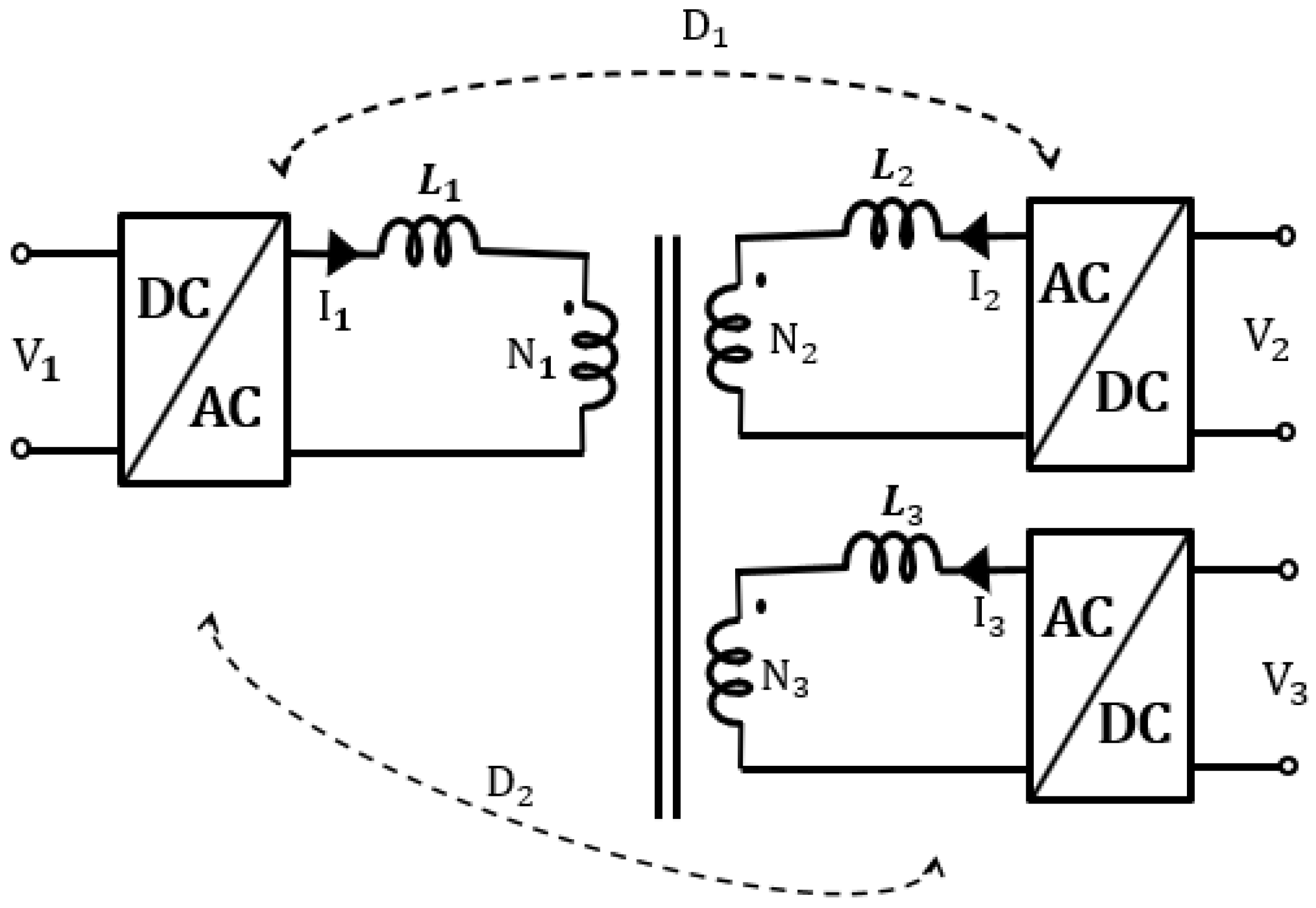
The multi-port or multi-winding-based DC–DC converter enables the interconnection of multiple energy sources and systems; this can be especially useful in DC microgrids for interconnecting different renewable energy power busses. In contrast to multi-port DC–DC converters that employ separate transformers for isolation at each module, thereby increasing the total weight of the converter, the converter researched in this work makes use of a single multi-winding transformer for isolation, which interconnects the different ports. This sees the reduction of isolation transformers leading to a significant increase in power density due to the reduction of the isolation transformer core and power conversion stages. A block representation of the three-port converter is as shown in Figure 1. It makes use of a single three-winding high-frequency transformer, interconnecting three ports [1,2,3].
The isolated three-port DC–DC converter is a multi-winding-based DC–DC converter that transfers power based on the phase difference between the switching signals of the sending and the receiving port(s). The isolated three-port DC–DC converter, as with the case of any other phase-shifted DC–DC converter, suffers from high backflow power, and this backflow power is known to be immanent in DC–DC converters that are phase-shifted. In simple terms, backflow power can be defined as the power that “flows back” to the transmitting source. Additionally, it is the main cause of system loss, since it flows contrary to the active power of the converter [4,5].
Although much work has been carried out on the multi-winding-based DC–DC converter, especially on the three-port converter, it still faces some limitations, which over time have been investigated by different authors [6,7,8]. Since the main goal of this research was efficiency improvement and stress reduction by eliminating the backflow power, the literature focuses on that aspect. Ref. [8] presents a method of efficiency improvement on the TAB converter by optimizing conduction loss. This was realized by minimizing the true RMS current instead of the fundamental part alone, as is the case in other studies.
The backflow power discussed in this paper contributes significantly to the reactive power in phase-shifted DC converters with an isolation transformer. On that note, we reviewed the following journals. Ref. [9] defined reactive power as negative power that flows back to the input source, while [4,10,11] defined reactive power as the reactive power consumed by the converter’s inductor with no fundamental frequency approximation of the voltage and currents. What [9] referred to as “reactive power” is actually what is referred to as “backflow power” in this paper. However, since the backflow power is the major contributor to the reactive power in the converter, the backflow power can then be interchangeably referred to as the system’s reactive power. The authors of [9] distinctly showed how minimizing the reactive (backflow) power positively influences the overall efficiency. The result of [4] presents a neural network model for the minimization of reactive power in a DAB converter, while [10] presented equations (solutions) for the total elimination of the reactive power from a DAB converter, and its results were outstanding. Ref. [9] presents a novel DPS control scheme to eliminate reactive power from a DAB converter. The algorithm presented in [9] is what was adopted by this work and applied to the three-port converter for backflow power elimination. Ref. [12] presents a method of reducing loss by adding a phase shift between diagonal switches of the primary, which also adds the degree of freedom of control. Ref. [13] researched on a resonant solid-state transformer (SST) aimed at minimizing the reactive currents. It features a phase-shifting mechanism that uses additional phase shifts on the secondary and tertiary switching signals but not the primary, resulting in a square voltage waveform on the primary side. Thus, [12,13] are the exact opposite in terms of switching though both achieved the aim of reactive power reduction. These works are different from that presented in this paper in that—in addition to the normal angle between the transformer voltages at the first (primary) winding and second (secondary) winding, primary and third (tertiary) winding—another phase shift is added between the diagonal switching signals of all ports. This creates a three-level voltage waveform on all transformer terminals. Ref. [14] presents a scheme for interconnecting modular multilevel converters, which also minimizes circulating power and overall system loss. Here, the control algorithm is dependent on the polarity of the power at the different output ports and does not make use of the fixed DPS control; moreover, the implemented topology is different from that used in this paper. This paper’s authors presented a study that compares the SPS and the DPS control scheme when applied to a TAB converter [15]. Ref. [15]’s research proposes the control characteristics analysis when the triple active bridge converter is controlled by two methods (the SPS and the DPS). In particular, when the triple active bridge converter is controlled by the SPS and DPS methods, harmonics, power characteristics, and backflow power representing loss are compared and analyzed.
As far as we know, this is the first time a detailed analysis of the backflow power present in a three-port DC–DC converter operating on the DPS control scheme is researched. This paper proposes a method to eliminate backflow power that is a causative component of power loss. Additionally, this paper applies the proposed method to an isolated three-port bidirectional DC–DC converter and proposes the characteristics of eliminating backflow power according to the proposed conditions. The work applies the DPS control algorithm on all three ports of the converter. the DPS scheme makes use of an extra phase shift angle between the switching signals of the diagonally placed semiconductor switches of each H-bridge of the converter. This results in a three-level step voltage profile at the transformer terminals. The mathematical description presented in this work results in not only a solution for backflow power but also solutions for the power present at each port of the three-port converter with full DPS control. With this control scheme, in addition to rightly choosing the high-frequency isolation transformer specifications, it is possible to achieve zero Backflow power, thereby drastically improving the overall system efficiency.
Section 2 presents the method; this includes the circuit description and the backflow power analysis in both the SPS and DPS control algorithms. The derived equations and waveforms are presented in Section 3, under the Results and Discussion. Lastly, Section 4 is the conclusion of the work.
This paper’s authors presented a study that compares the SPS and the DPS control scheme when applied to a TAB converter [15]. Ref. [15]’s research proposes the control characteristics analysis when the triple active bridge converter is controlled by two methods (the single phase shift (SPS) and the dual phase shift (DPS)). In particular, when the triple active bridge converter is controlled by SPS and DPS methods, harmonics, power characteristics, and backflow power representing loss are compared and analyzed.
As far as we know, this is the first time a detailed analysis of the backflow power present in a three-port DC–DC converter operating on the DPS control scheme is researched. This paper proposes a method to eliminate backflow power, which is a causative component of power loss. Additionally, this paper applies the proposed method to an isolated three-port bidirectional DC–DC converter and proposes the characteristics of eliminating backflow power according to the proposed conditions.
This work applies the DPS control algorithm on all three ports of the converter. The DPS scheme makes use of an extra phase shift angle between the switching signals of the diagonally placed semiconductor switches of each H-bridge of the converter. This results in a three-level step voltage profile at the transformer terminals. The mathematical description presented in this work results in not only a solution for the backflow power but also solutions for the power present at each port of the three-port converter with full DPS control. With this control scheme, in addition to rightly choosing the high-frequency isolation transformer specifications, it is possible to achieve zero backflow power, thereby drastically improving the overall system efficiency.
2. Method
2.1. Circuit Description
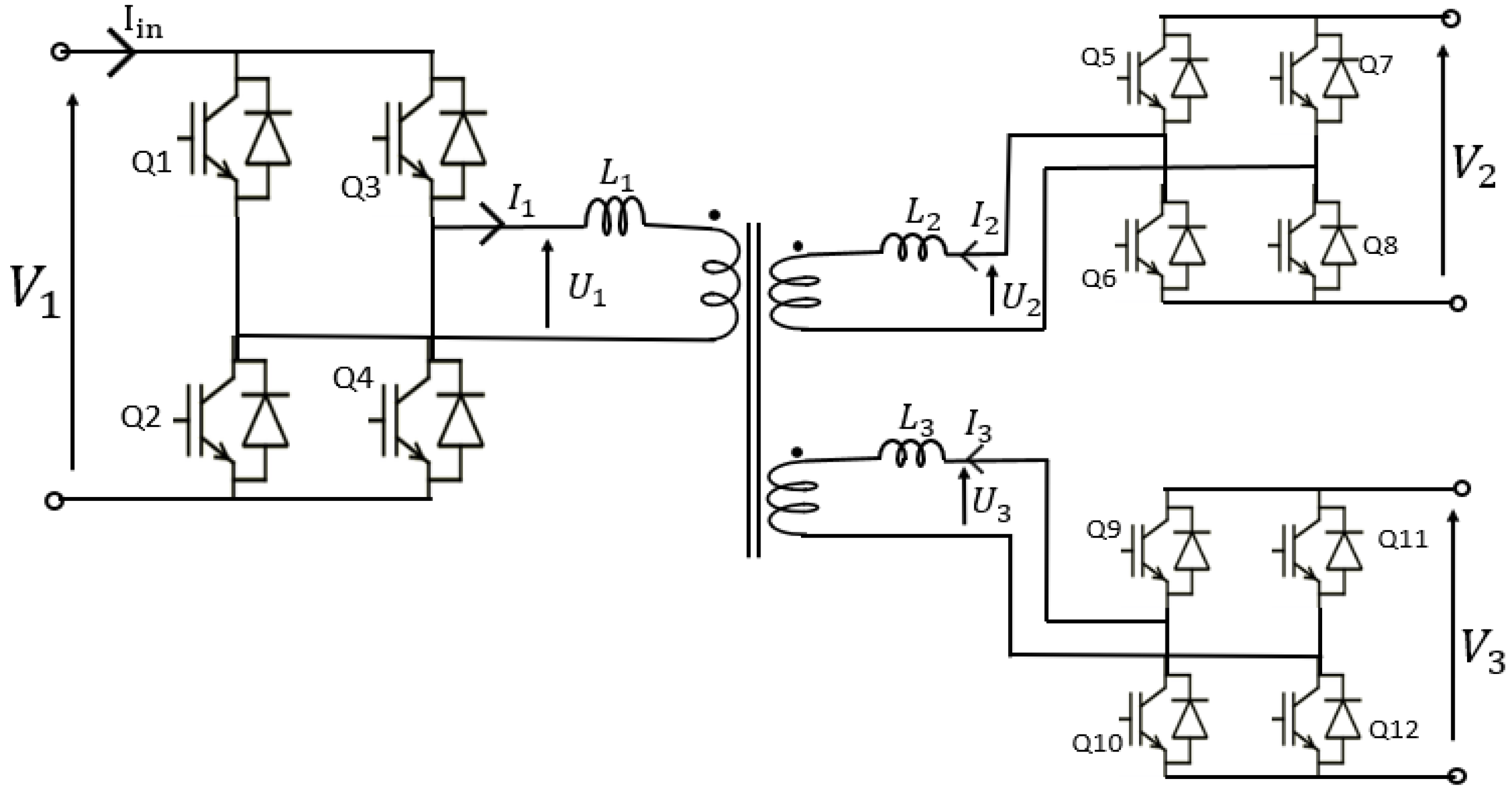
Figure 2 shows the three-port DC–DC converter, and it is described as follows: This converter comprises a single transformer core with three windings that are connected to separate H-bridges. Taking the first port (connected to the primary winding of the transformer) of the converter as a reference, the phase shift ratio between the primary and secondary voltages of the transformer is while the ratio between the primary and tertiary is . and where and are the corresponding phase shift angles between the secondary and tertiary with respect to the primary. , and are the DC-linked voltages of the primary, secondary, and tertiary ports, respectively. , , and represent the number of turns of the transformer’s primary, secondary, and tertiary winding, respectively, while , , and are the corresponding transformer voltages at the different winding terminals. is the input current to port 1, while , , and are the transformer currents for each winding. , , and are the corresponding leakage inductance for the transformer windings.
Table 1 shows the converter specifications that were used for the simulation.
For this work, all the DC linked voltages are the same ( = = ), all the windings are of the same number of turns, the leakage inductances are the same ( = = ), so too are the phase-shift ratios ( = or = ). With these assumptions, the voltage conversion ratios are all equal to 1. i.e., , where = and = .
2.2. Backflow Power in SPS Operation
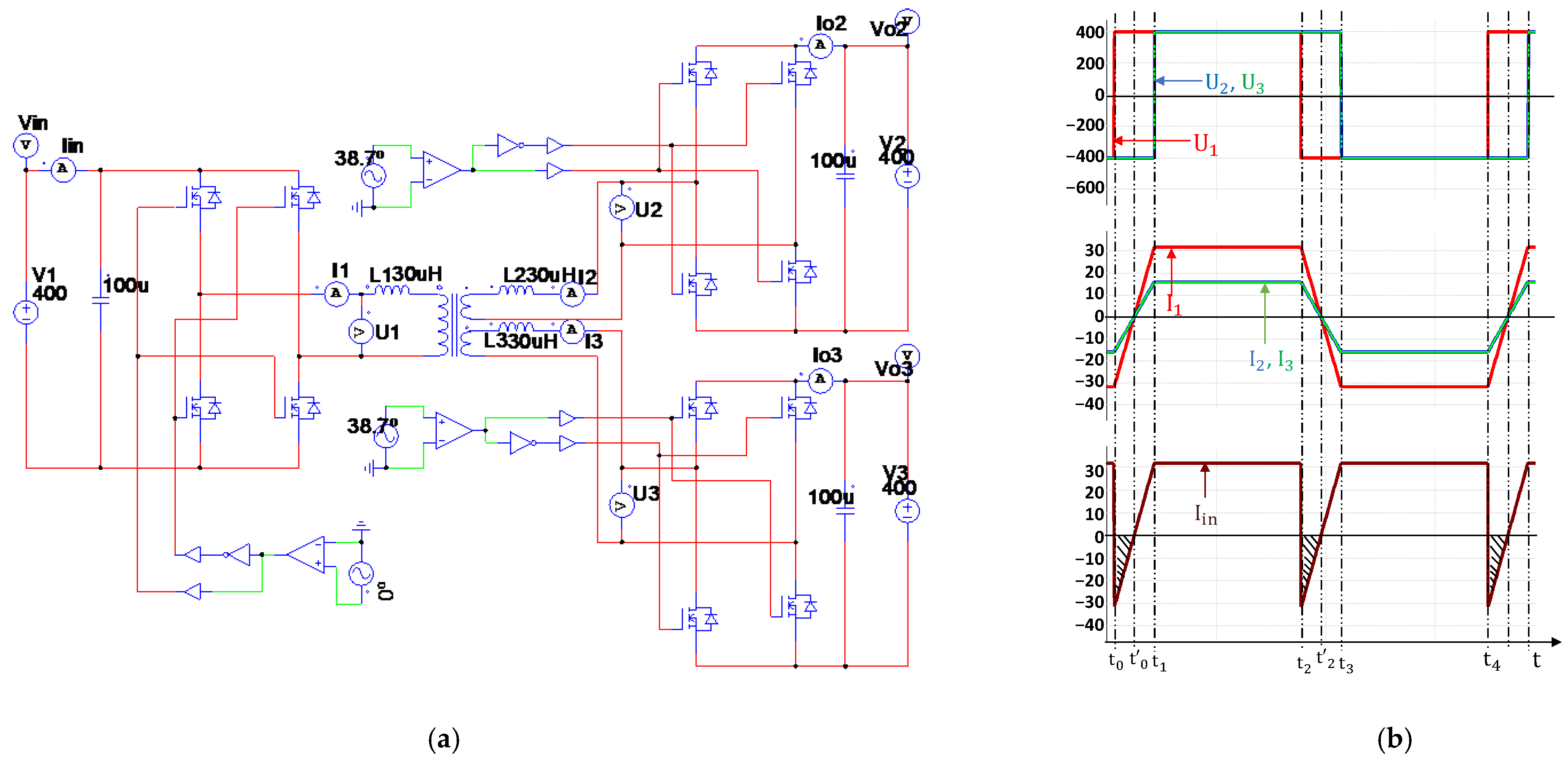
In the SPS control of the three-port converter, each H-bridge is controlled by a modulated signal with a duty ratio of 0.5, and the secondary and tertiary H-bridge signals are phase-shifted by the ratios and , respectively, with respect to the primary H-bridge (cell). This results in square voltage waveforms at the transformer terminals as shown on the first curve of Figure 3b, while the PSIM simulated circuit is as shown in Figure 3a. The second curve of Figure 3b illustrates the transformer currents (leakage inductance currents) while the last is the input current waveform. From Figure 3b, it is observed that the voltage across the primary winding () becomes positive (from −400 V to 400 V) when whereas the corresponding current () turns positive when . So too, the same primary voltage becomes negative (from −400 V to 400 V) when , whereas the current only turns negative when . This results in a phase difference between the primary current and voltage during the periods and . This phase difference leads to a negative power (since either the voltage is negative when the current is positive, or the current is negative when the voltage is positive) that flows in the reverse direction. This power is referred to as the power that “flows back” to the source or backflow power. This occurs twice within one switching cycle and this power is represented by the area below the zero mark on the input current waveform (i.e., the shaded area of the last curve of Figure 3b). This power can be obtained by averaging the shaded area over half the period and then multiplying by the input voltage. This can be obtained using the integral equation provided in Equation (1).
Table 2 shows the switching cycle for one period for the SPS control.
The equation for the backflow power present in an SPS-controlled three-port converter based on the transformer current and voltage waveforms is calculated by Equation (1).
where xy can be 12 and 13.
The time period is calculated by Equation (2)
The peak current at time is calculated by Equation (3)
The area of the shaded region is
Thus, the average current is shown as
The backflow power between winding 1 and 2 is calculated by Equation (6)
Backflow power between winding 1 and 3 is calculated by Equation (7)
The total backflow power is
In our work, when = = and k = , the total backflow power becomes
To further reduce the equation, when k = 1,
From Equation (10), it is seen that there is always some backflow power with the SPS control scheme except for when the phase shift ration , at which point the converter is off.
2.3. Backflow Power in DPS Operation
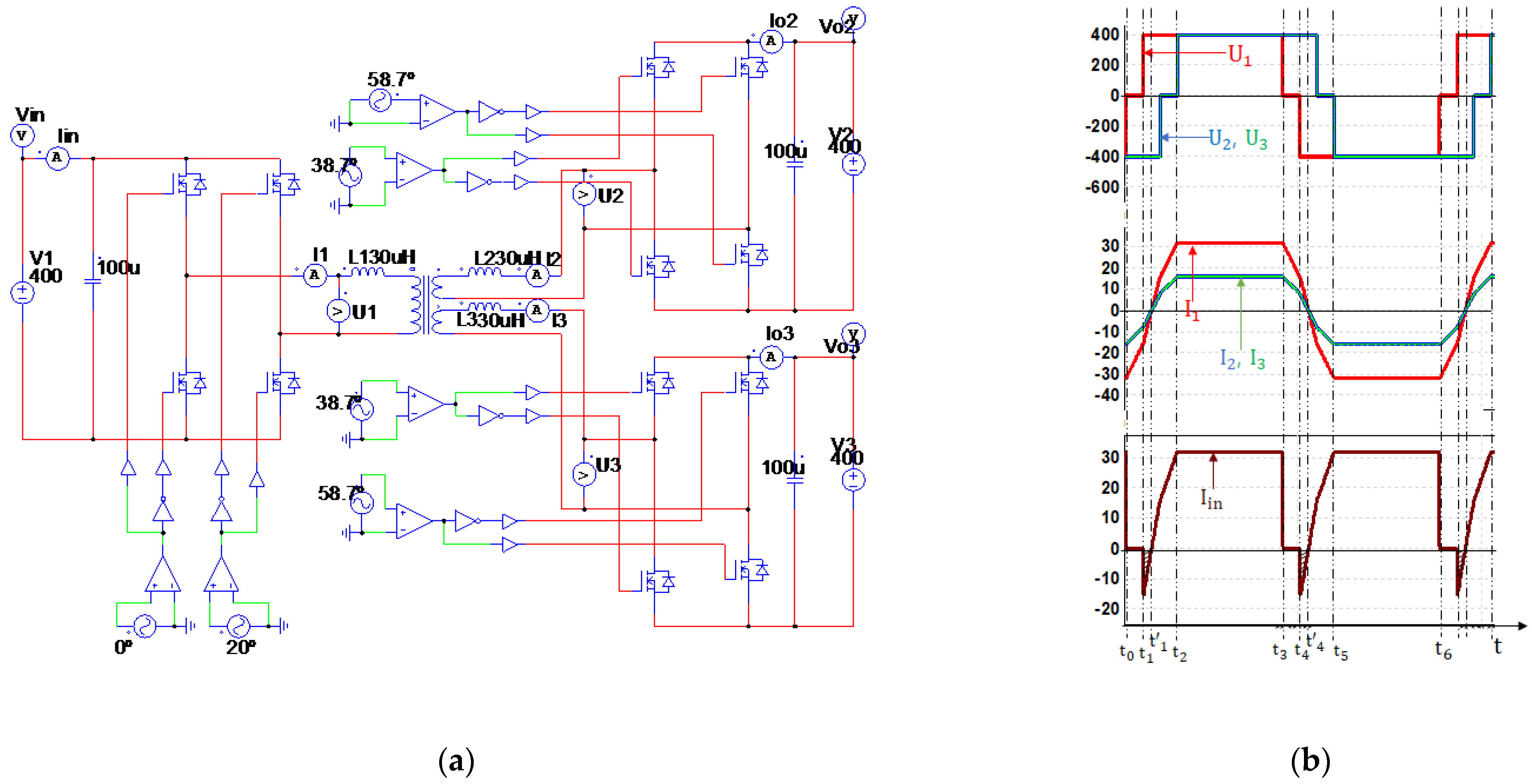
In DPS, each H-bridge has an extra phase angle () between its diagonal switching signals (the added angle is referred to as the internal phase shift angle). For the DPS, extra signal generators are required for each H-bridge so as to create the internal phase-shift angle. Thus, instead of the traditional square voltage profile, a three-level step voltage waveform with the inclusion of a zero-voltage level is generated at the transformer terminals (the first curves of Figure 4b). This phase shift angle corresponds to a phase shift ratio of . i.e., . The simulated circuit and the corresponding waveforms are, respectively, shown in Figure 4a,b. The transformer currents are represented by , , and of Figure 4b. Following the same description as with the SPS control scheme, on the last curve, the shaded area is the backflow power (input current curve). Contrary to the SPS, the backflow region caused by the phase difference between the transformer voltage and current for the DPS start from and , and end at and , respectively, for a single switching period. This is as shown in the last curve of Figure 4b and it is seen that this region spans a smaller period compared to the SPS implying lesser backflow power with the use of DPS control scheme. Table 3 presents the switching cycle for one period with the DPS control.
Using Table 3 and Figure 4b, the relations for obtaining the backflow power with the DPS algorithm are presented in Equations (11)–(20).
The time period is calculated by Equation (12) while the peak current at time is calculated by Equation (13).
The area of the shaded region is
Thus, the average current is calculated as
Therefore, the backflow power between winding 1 and 2, and winding 1 and 3 is calculated by Equations (16) and (17), respectively.
The total Backflow power is calculated by
When = = and k = , the total backflow power becomes
Equation (20) provides a further reduced form of Equation (19) by letting k = 1
From Equation (20), when , there is zero power backflow. The next section (Section 3; results) provides a simulation of this.
3. Results and Discursion
3.1. Backflow Power Eliminated with DPS
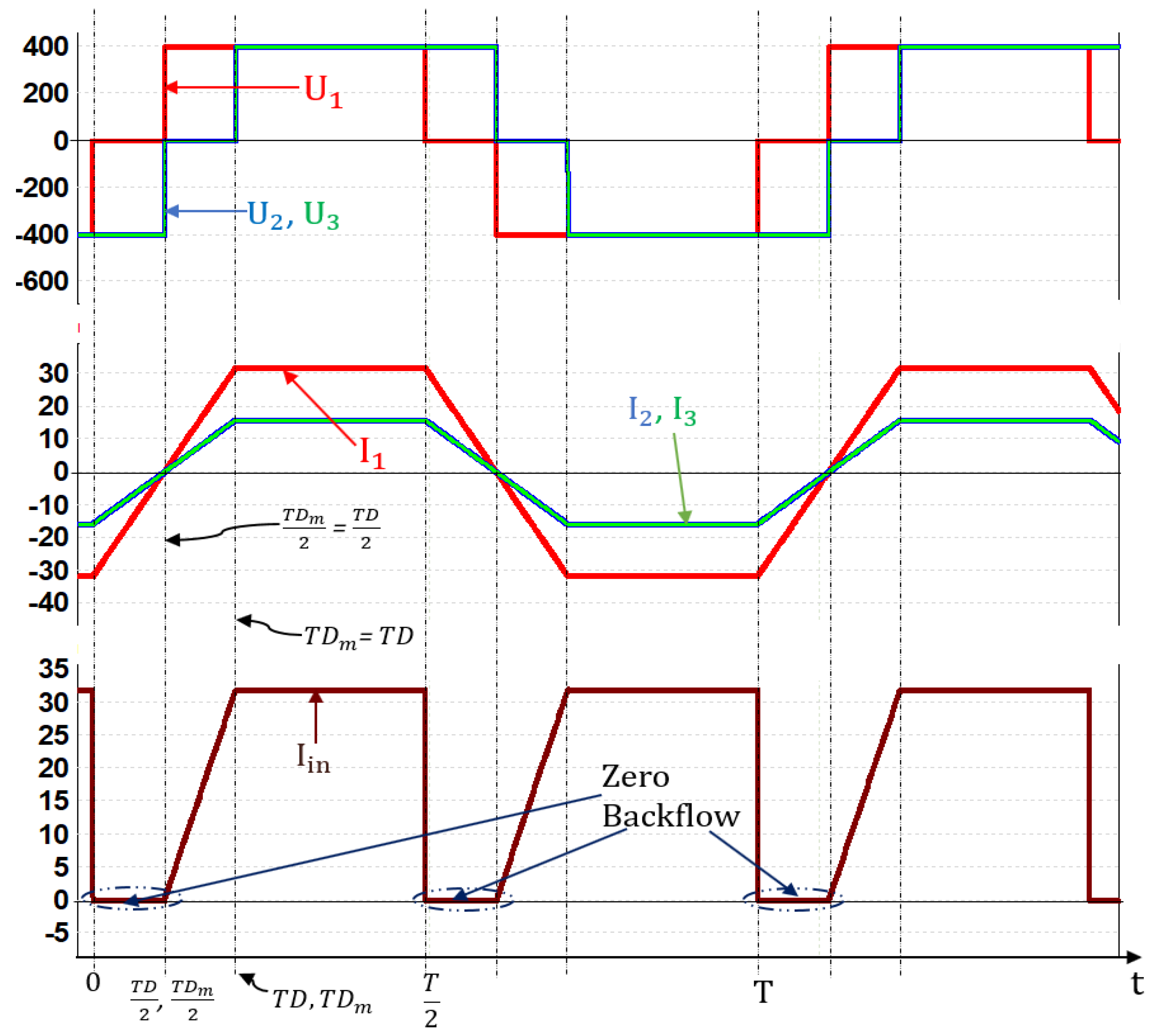
From Section 2, under the “Backflow Power in DPS Operation” subsection, Equation (20) illustrates that it is possible to eliminate the backflow power when the added (inner) phase-shift angle is equal to the outer phase-shift angle ( 38.7° (this is illustrated in Figure 5)). On this figure it is seen that the phase difference between the transformer voltages and their corresponding currents is cut off (the phase difference is zero), i.e., the current and voltage waveforms cuts across the zero line at same time (becomes negative and/or positive at the same time: at and at , respectively), this is visible from the first and middle curves of Figure 5. Due to the elimination of the phase difference, the backflow power is therefore eliminated from the three-port converter since there is no power “flow back”. Moreover, for the time period in which the current is already above or below the zero line, the added phase-shift angle clamps the voltage to zero, leading to zero-power transferred and thereby zero backflow power for that time period ( and within one switching cycle).
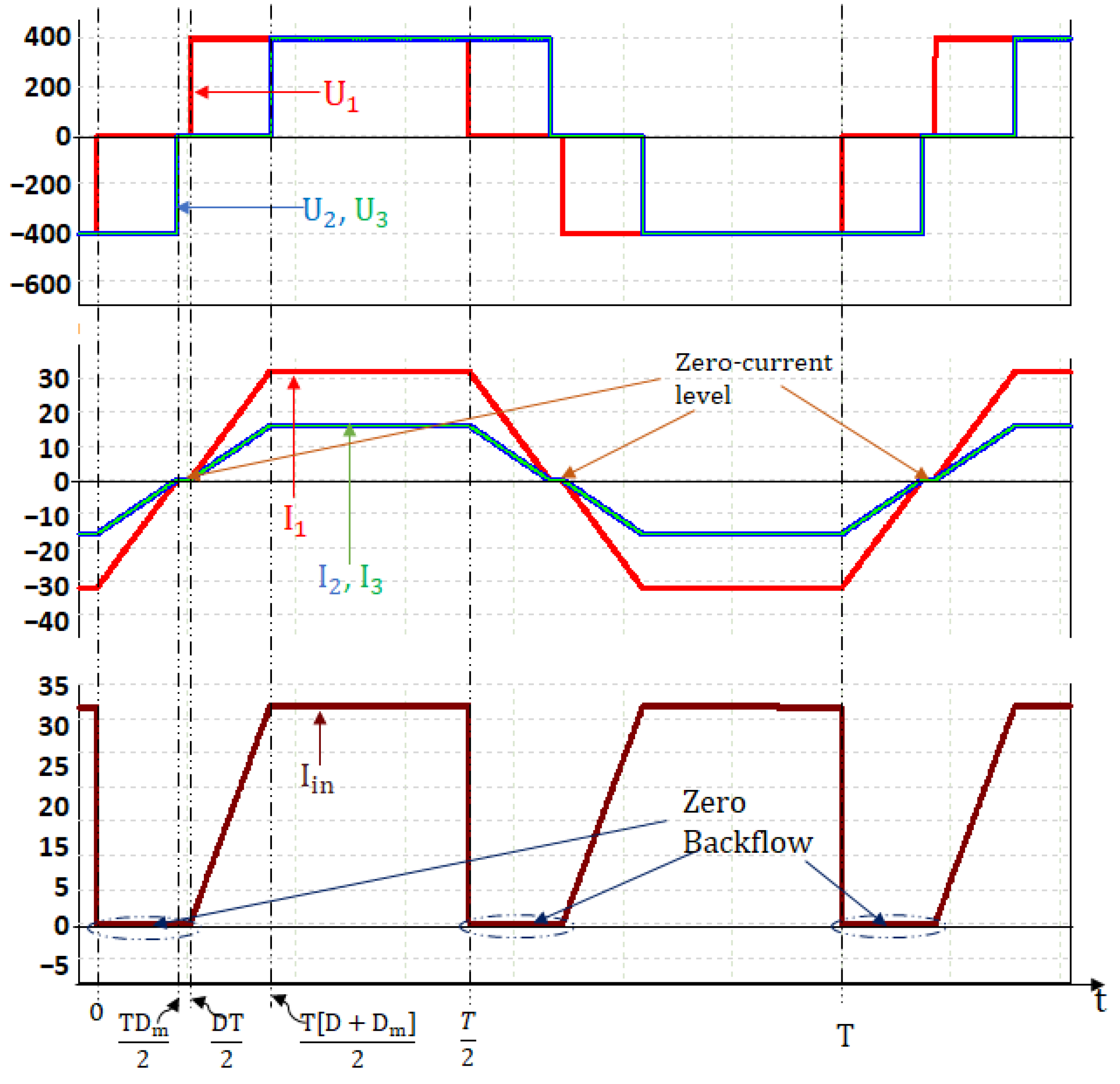
Based on further experimentation (simulations) on the converter, it is observed that the backflow power can also be eliminated when the inner phase shift angle, of the DPS control scheme, is greater than the outer phase shift angle, (as illustrated in Figure 6). For this simulation, 45° while the outer phase shift angle remained at 38.7°. Furthermore, it is observed that when the zero-level of the transformer voltages overlap (due to the inner phase-shift angle being greater than the outer phase-shift angle), the transformer currents are clamped to zero (this is seen on the middle curve of Figure 6, i.e., ), resulting in zero power being transferred during this period. When there is zero power transfer, there is consequently zero backflow power.
3.2. Characteristics of the Backflow Power and the Power Processed by the Converter
The power processed at the various ports based on the stated range of under the SPS control scheme is shown by Equations (21)–(23) while those for the DPS control scheme are shown by Equations (24)–(26).
For
In our work, were and , Equations (21)–(26) become Equations (27) and (28) for the SPS, and Equations (29) and (30) for the DPS
Differentiating Equation (27) with respect to and equating to zero for the maximum point we obtain
Therefore, the maximum transferable power of converter occurs at , and is calculated by Equation (31). This value is used for the following characterization (i.e., the unified value).
Partial differentiating Equation (29), with respect to then equating to zero for the maximum point we calculate
The maximum power for the DPS control scheme occurs when
3.2.1. Characterization of the Backflow Power
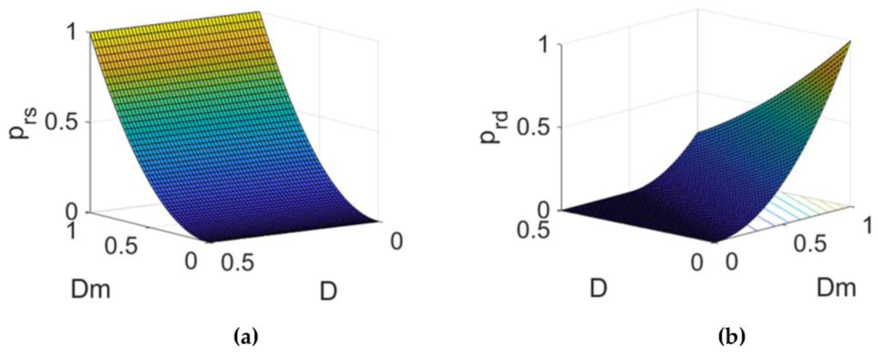
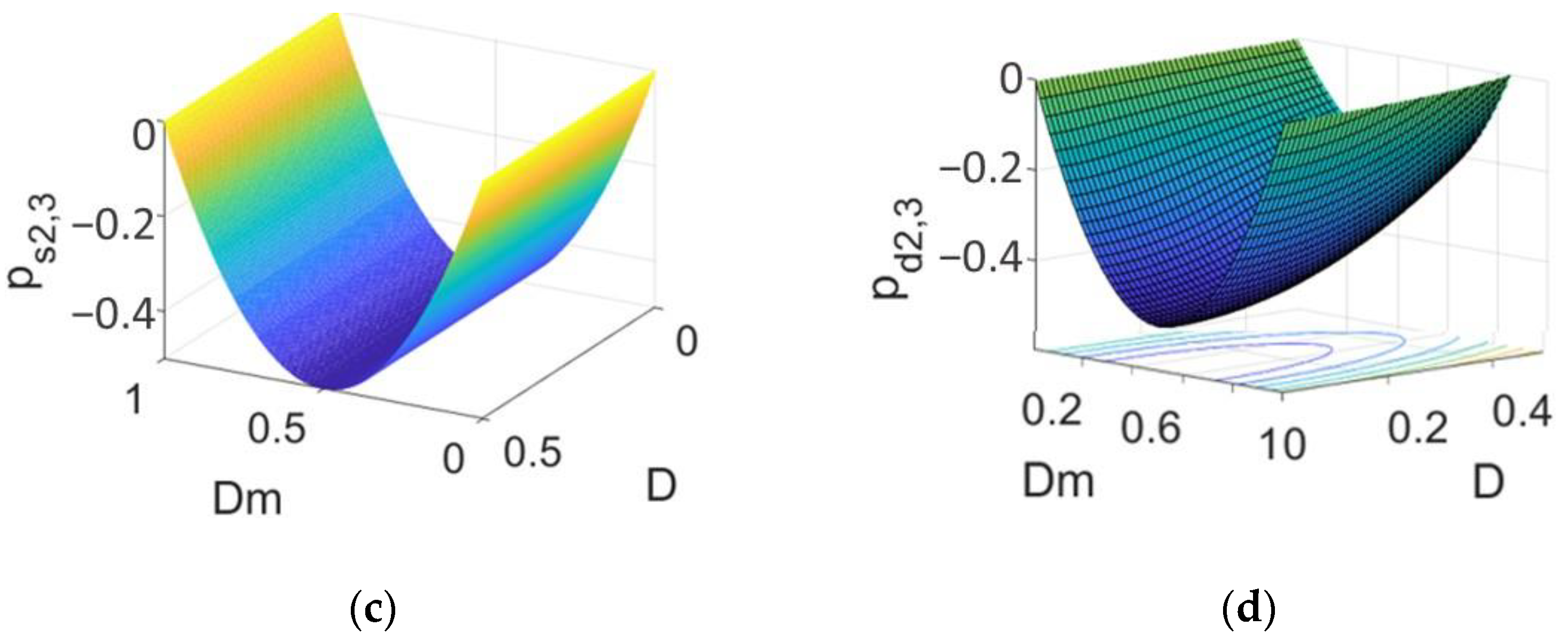
The unified value for the backflow power in the SPS-controlled three-port converter is calculated by Equation (32), while that for the DPS-controlled three-port converter is calculated by Equation (33). The corresponding 3D surface plots are illustrated in Figure 7a,b.
Figure 7a shows that although the internal phase shift D has no effect on the backflow power, it increases exponentially as the outer phase-shift increases. Moreover, the plot confirms the derived Equation (10), which illustrates that the backflow power can only be zero when the converter is not transmitting power. Figure 7b also confirms the statement under Equation (20), which illustrates that the backflow power is zero when the internal phase-shift is equal the external phase-shift Moreover, as illustrated on Figure 6, the backflow power is eliminated when the internal phase-shift is greater than the external phase-shift; this is also discernible from Figure 7b. Furthermore, observations reveal that the backflow power decreases as the inner phase-shift angle increases.
3.2.2. Characterization of the Processed Power at the Various Ports
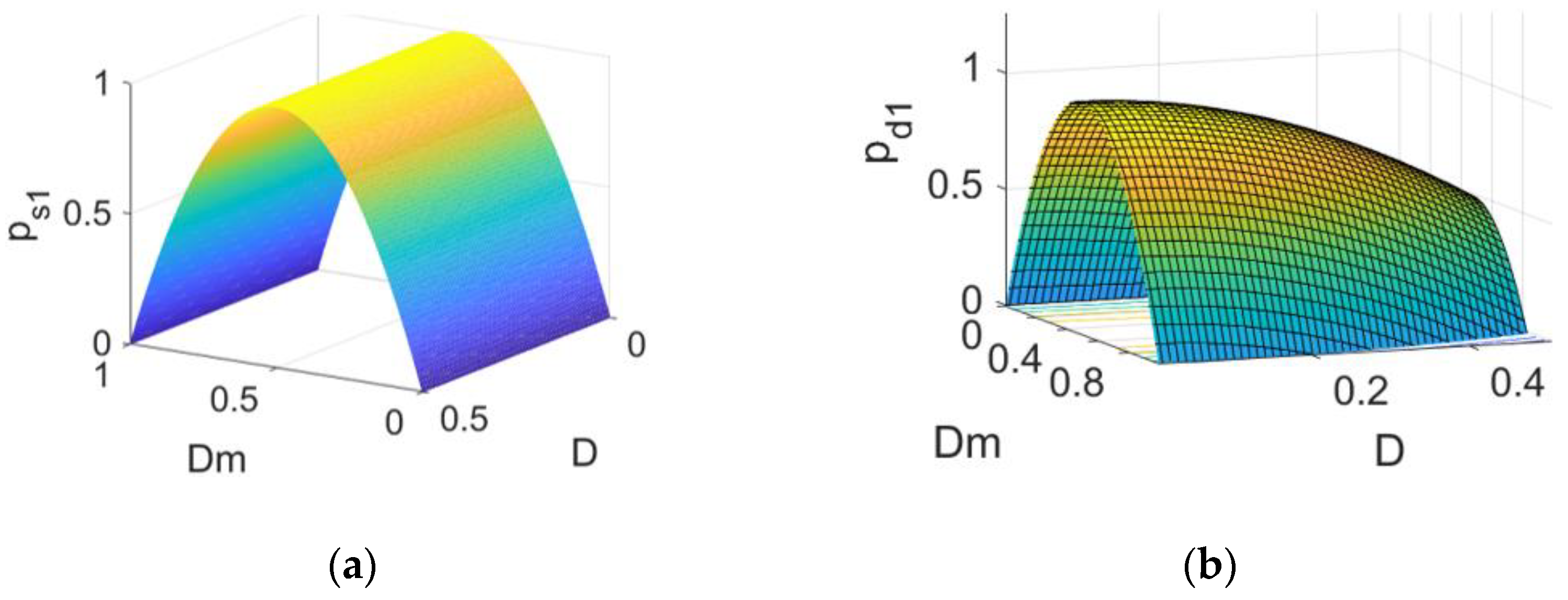
The equations for the unified power at the different ports are Equations (34)–(37). Where is the unified power at port one using SPS control, is that at port one using DPS control, , and are the unified powers at ports two and three for the SPS and DPS, respectively. Figure 8 illustrates the characteristics of the corresponding unified powers.
According to Figure 8a (power at port 1 for the SPS control scheme), the maximum power occurs at , and D does not affect it. For the DPS control, at port 1 (Figure 8b), maximum power is reached at . This affirms the partial derivation of Equation (29), and this power reduces as the added phase shift (D) increases. Ports 2 and 3 exhibit the same behavior for the corresponding control schemes, except that the maximum power is half of that at port 1 for the two control schemes.
4. Conclusions
The purpose of this work was to eliminate the backflow power present in three-port DC–DC converters. As seen in the literature, backflow power is immanent in DC–DC converters that are phase-shifted, and it is the main cause of loss. Still, in the literature it is seen that different switching techniques aimed at reducing the losses present in similar converters have been proposed and implemented. This work introduces the use of the DPS control scheme on the three-port converter for the purpose of backflow power elimination and subsequently increases the overall system efficiency. This work sees the mathematical analysis of not only the backflow power for both schemes, but also the full analysis of the converter as well. This analysis led to the derivation of the equations for the power at the various ports and also the backflow power with SPS and DPS. From this equation, a mathematical solution for zero backflow power was obtained, i.e., the backflow power is zero when the internal phase-shift angle () is equal to the external phase-shift angle (). This solution was confirmed by simulation with values of , which obtained zero backflow power. Other simulations showed that the backflow power can also be eliminated when the internal phase-shift angle of the DPS is greater than the external phase-shift. As a result, this work achieved its primary objective. It was also observed that, unless the added phase-shift of the DPS scheme is zero, backflow power will always be greater with the SPS algorithm than the DPS. This affords more credit to the DPS control algorithm.
For future works, more research should be carried out on the backflow power of the three-port converter with a voltage conversion ratio (k) different from 1.
Author Contributions
Conceptualization, N.N.K.; methodology, N.N.K.; software, N.N.K.; validation, N.N.K., J.-S.K. and D.-K.K.; formal analysis, N.N.K. and D.-K.K.; investigation, N.N.K.; resources, N.N.K. and D.-K.K.; data curation, N.N.K.; writing—original draft preparation, N.N.K.; writing—review and editing, N.N.K., J.-S.K. and D.-K.K.; visualization, N.N.K.; supervision, D.-K.K. All authors have read and agreed to the published version of the manuscript.
Funding
This research was financially supported by the Ministry of Trade, Industry and Energy(MOTIE) and Korea Institute for Advancement of Technology(KIAT) through the National Innovation Cluster R&D program (P0015360_Development and demonstration of Multi-circuit Power Conversion Device for protection coordination of DC distribution network). This work was supported by the Gwangju Jeonnam local EnergyCluster Human Resources Development of the Korea Insitute of Energy Technology Evaluation and Planning(KETEP) grant funded by the Korea government Ministry of Knowledge Economy (No. 20214000000560).
Data Availability Statement
Not applicable.
Conflicts of Interest
The authors declare no conflict of interest.
Abbreviations
| DPS | Dual phase shift |
| SPS | Single phase shift |
| PSIM | Power SIM |
| TAB | Triple active bridge |
| RMS | Root mean square |
| DAB | Dual active bridge |
| SST | Solid state transformer |
| Symbols | |
| Internal phase-shift ratio | |
| Phase-shift ratio between ports 1 and 2 | |
| Phase-shift ratio between ports 1 and 3 | |
| Internal phase-shift angle | |
| Phase-shift angle between ports 1 and 2 | |
| Phase-shift angle between ports 1 and 3 | |
| DC-linked voltages at the different ports | |
| Voltages at the transformer terminals | |
| Number of turns of the different windings | |
| Transformer currents | |
| Leakage inductance of the windings | |
| Converter’s input current | |
| Voltage conversion ratios | |
| Backflow power with SPS control | |
| Backflow power with DPS control | |
| A | Area of the backflow region |
| T | Switching period |
| Average current | |
| Backflow power between ports 1 and 2 | |
| Backflow power between ports 1 and 3 | |
| Power processed at the ports with SPS | |
| Power processed at the ports with DPS | |
| Maximum possible power | |
| Ratio of backflow power with SPS on | |
| Ratio of backflow power with DPS on | |
| Ratio of power at the ports with SPS on | |
| Ratio of power at the ports with DPS on |
References
- Kim, J.-C.; Huh, J.-H.; Ko, J.-S. Optimization Design and Test Bed of Fuzzy Control Rule Base for PV System MPPT in Micro Grid. Sustainability 2020, 12, 3763. [Google Scholar] [CrossRef]
- Jung, S.; Yoon, Y.T.; Huh, J.-H. An Efficient Micro Grid Optimization Theory. Mathematics 2020, 8, 560. [Google Scholar] [CrossRef] [Green Version]
- Kim, J.-C.; Huh, J.-H.; Ko, J.-S. Improvement of MPPT Control Performance Using Fuzzy Control and VGPI in the PV System for Micro Grid. Sustainability 2019, 11, 5891. [Google Scholar] [CrossRef] [Green Version]
- Harrye, Y.A.; Ahmed, K.H.; Aboushady, A.A. Reactive power minimization of dual active bridge DC/DC converter with triple phase shift control using neural network. In Proceedings of the 2014 International Conference on Renewable Energy Research and Application (ICRERA), Milwaukee, WI, USA, 19–22 October 2014; pp. 566–571. [Google Scholar] [CrossRef]
- Zhao, B.; Yu, Q.; Sun, W. Extended-Phase-Shift Control of Isolated Bidirectional DC–DC Converter for Power Distribution in Microgrid. IEEE Trans. Power Electron. 2012, 27, 4667–4680. [Google Scholar] [CrossRef]
- Pereira, T.; Hoffmann, F.; Liserre, M. Potentials and Challenges of Multiwinding Transformer-Based DC-DC Converters for Solid-State Transformer. In Proceedings of the IECON 2021—47th Annual Conference of the IEEE Industrial Electronics Society, Toronto, ON, Canada, 13–16 October 2021; pp. 1–6. [Google Scholar] [CrossRef]
- Koneh, N.N.; Ko, J.-S.; Kim, D.-K. Characteristics of an AC/DC Hybrid Converter According to Load Fluctuation. Int. J. Eng. Trends Technol. 2021, 69, 205–210. [Google Scholar] [CrossRef]
- Ibrahim, A.A.; Caldognetto, T.; Mattavelli, P. Conduction Loss Reduction of Isolated Bidirectional DC-DC Triple Active Bridge. In Proceedings of the 2021 IEEE Fourth International Conference on DC Microgrids (ICDCM), Arlington, VA, USA, 18–21 July 2021; pp. 1–8. [Google Scholar] [CrossRef]
- Bai, H.; Mi, C. Eliminate Reactive Power and Increase System Efficiency of Isolated Bidirectional Dual-Active-Bridge DC–DC Converters Using Novel Dual-Phase-Shift Control. IEEE Trans. Power Electron. 2008, 23, 2905–2914. [Google Scholar] [CrossRef]
- Rahman, M.I.; Jovcic, D.; Ahmed, K.H. Reactive current optimization for high power dual active bridge DC/DC converter. In Proceedings of the 2013 IEEE Grenoble Conference, Grenoble, France, 16–20 June 2013; pp. 1–6. [Google Scholar] [CrossRef]
- Jain, A.K.; Ayyanar, R. Pwm control of dual active bridge: Comprehensive analysis and experimental verification. IEEE Trans. Power Electron. 2011, 26, 1215–1227. [Google Scholar] [CrossRef]
- Katagiri, K.; Nakagawa, S.; Kurosawa, K.; Arai, J.; Kado, Y.; Wada, K. Power flow control of triple active bridge converter equipped with AC/DC converter for constructing autonomous hybrid AC/DC microgrid systems. In Proceedings of the IECON 2017—43rd Annual Conference of the IEEE Industrial Electronics Society, Beijing, China, 29 October–1 November 2017; pp. 1441–1446. [Google Scholar] [CrossRef]
- Malan, W.L.; Vilathgamuwa, D.M.; Walker, G.R.; Hiller, M. A three port resonant solid-state transformer with minimized circulating reactive currents in the high frequency link. In Proceedings of the 2016 IEEE 2nd Annual Southern Power Electronics Conference (SPEC), Auckland, New Zealand, 5–8 December 2016; pp. 1–6. [Google Scholar] [CrossRef]
- Yapa, R.; Forsyth, A. Extended soft switching operation of the triple active bridge converter. In Proceedings of the 6th IET International Conference on Power Electronics, Machines and Drives (PEMD 2012), Bristol, UK, 27–29 March 2012; pp. 1–6. [Google Scholar] [CrossRef]
- Koneh, N.N.; Ko, J.-S.; Kim, D.-K. Simulations of the Comparative Study of the Single-Phase Shift and the Dual-Phase Shift-Controlled Triple Active Bridge Converter. Electronics 2022, 11, 3274. [Google Scholar] [CrossRef]
Figure 1.
Block diagram representation of the three-winding transformer-based DC–DC converter.

Figure 2.
The three-port DC–DC converter showing the different H-bridges.

Figure 3.
SPS operation (a) simulated circuit and (b) corresponding waveforms.

Figure 4.
DPS operation (a) simulated circuit and (b) corresponding waveforms.

Figure 5.
Voltage and current waveforms when .

Figure 6.
Voltage and current waveforms when .

Figure 7.
Backflow power characteristic (a) SPS control and (b) DPS control.

Figure 8.
Characteristic of the power at the different ports for the SPS and the DPS (a) at port one for SPS, (b) at port one for DPS, (c) at ports 2 and 3 for SPS, and (d) at ports 2 and 3 for DPS.
Figure 8.
Characteristic of the power at the different ports for the SPS and the DPS (a) at port one for SPS, (b) at port one for DPS, (c) at ports 2 and 3 for SPS, and (d) at ports 2 and 3 for DPS.


Table 1.
Converter specifications.
| Specification | Symbol | Value |
|---|---|---|
| DC linked voltages (v) | ||
| Switching frequency (kHz) | ||
| Turn ratio | ||
| Leakage inductance (µH) | ||
| Power (kw) | 10 | |
| Phase shift ratio | 0.215 | |
| Phase shift angle | 38.7° | |
| Internal phase shift angle | 20° |
Table 2.
Switching cycle for one period for the SPS.
| Time | Value |
|---|---|
| 0 | |
| T/2 | |
| T[1 + ]/2 | |
| T |
Table 3.
Switching cycle for one period with the DPS control.
| Time | Value |
|---|---|
| 0 | |
| T/2 | |
| /2 | |
| T |
Disclaimer/Publisher’s Note: The statements, opinions and data contained in all publications are solely those of the individual author(s) and contributor(s) and not of MDPI and/or the editor(s). MDPI and/or the editor(s) disclaim responsibility for any injury to people or property resulting from any ideas, methods, instructions or products referred to in the content. |
© 2022 by the authors. Licensee MDPI, Basel, Switzerland. This article is an open access article distributed under the terms and conditions of the Creative Commons Attribution (CC BY) license (https://creativecommons.org/licenses/by/4.0/).
Share and Cite
MDPI and ACS Style
Koneh, N.N.; Ko, J.-S.; Kim, D.-K. Simulations to Eliminate Backflow Power in an Isolated Three-Port Bidirectional DC–DC Converter. Energies 2023, 16, 450. https://0-doi-org.brum.beds.ac.uk/10.3390/en16010450
AMA Style
Koneh NN, Ko J-S, Kim D-K. Simulations to Eliminate Backflow Power in an Isolated Three-Port Bidirectional DC–DC Converter. Energies. 2023; 16(1):450. https://0-doi-org.brum.beds.ac.uk/10.3390/en16010450
Chicago/Turabian StyleKoneh, Norbert Njuanyi, Jae-Sub Ko, and Dae-Kyong Kim. 2023. "Simulations to Eliminate Backflow Power in an Isolated Three-Port Bidirectional DC–DC Converter" Energies 16, no. 1: 450. https://0-doi-org.brum.beds.ac.uk/10.3390/en16010450
Note that from the first issue of 2016, this journal uses article numbers instead of page numbers. See further details here.