Article

Nanostructured Thermoelectric PbTe Thin Films with Ag Addition Deposited by Femtosecond Pulsed Laser Ablation

1
Istituto di Struttura della Materia (ISM)—Sez. Montelibretti, DiaTHEMA Laboratory, Consiglio Nazionale delle Ricerche, Via Salaria km 29.300, 00015 Monterotondo, Italy
2
Istituto di Struttura della Materia (ISM)—Sez. Tito Scalo, FemtoLab, Consiglio Nazionale delle Ricerche, Zona Industriale, 85050 Tito, Italy
3
Istituto di Metodologie per l’Analisi Ambientale (IMAA), Consiglio Nazionale delle Ricerche, Zona Industriale, 85050 Tito, Italy
4
Istituto per lo Studio dei Materiali Nanostrutturati (ISMN)—Sez. Montelibretti, Consiglio Nazionale delle Ricerche, Via Salaria km 29.300, 00015 Monterotondo, Italy
*
Author to whom correspondence should be addressed.
Submission received: 28 February 2023 / Revised: 28 March 2023 / Accepted: 30 March 2023 / Published: 3 April 2023
(This article belongs to the Special Issue Advanced Studies of Thermoelectric Systems)

Abstract

:
Pulsed laser deposition operated by an ultra-short laser beam was used to grow in a vacuum and at room temperature natively nanostructured thin films of lead telluride (PbTe) for thermoelectric applications. Different percentages of silver (Ag), from 0.5 to 20% of nominal concentration, were added to PbTe deposited on polished technical alumina substrates using a multi-target system. The surface morphology and chemical composition were analyzed by Scanning Electron Microscope and X-ray Photoelectron Spectroscopy, whereas the structural characteristics were investigated by X-ray Diffraction. Electrical resistivity as a function of the sample temperature was measured by the four-point probe method by highlighting a typical semiconducting behavior, apart from the sample with the maximum Ag concentration acting as a degenerate semiconductor, whereas the Seebeck coefficient measurements indicate n-type doping for all the samples. The power factor values (up to 14.9 µW cm−1 K−2 at 540 K for the nominal 10% Ag concentration sample) are competitive for low-power applications on flexible substrates, also presuming the achievement of a large reduction in the thermal conductivity thanks to the native nanostructuring.

1. Introduction

In the last decade, a great interest has been growing to find a way of developing efficient thermoelectric devices for the conversion of heat into electricity by exploiting the Seebeck effect [1,2], with the aim of re-using the large heat that is typically wasted in several industrial processes. Additionally, thermoelectric generators have been used to produce renewable energy, particularly for the conversion of concentrated solar radiation, both directly [3] or combined with thermionic generators [4,5]. The conversion efficiency of thermoelectric materials is characterized by the dimensionless figure of merit zT = S2σΤ/κ, where S, σ, T, and κ are the Seebeck coefficient, the electrical conductivity, the absolute temperature, and the thermal conductivity, respectively. Extensive and detailed studies have established, over a long period of time, that to achieve an optimal value of the coefficient zT, it is advisable to follow the strategy of the “phonon glass electron crystal” approach [6], which implies the creation of a material with a tailored structure that has, at the same time, low thermal conductivity (phonon glass), but high electrical conductivity (electron crystal). Consequently, several studies came to find a way to optimize thermoelectric material by maximizing its performance. Nanostructuring is the most diffused approach to improve zT, by enhancing the Seebeck coefficient via the quantum confinement effect and, at the same time, by decreasing thermal conductivity through enhanced phonon scattering at grain boundaries and interfaces [7,8,9,10]. Several complex nanostructures have been designed for thermoelectric materials: two-dimensional superlattice structures, one-dimensional nano-systems, and zero-dimensional nanoplates and nanoparticles [11,12,13,14,15].
Compared with bulky systems, the production of thin films has the noteworthy advantage of being compatible with semiconductor technology. Additionally, thin films can be easily applied in the fabrication of thermoelectric nano-devices, the research of which is becoming extremely important thanks to the continuous requirements of miniaturization and flexibility for the novel application scenario of the Internet of Things [16,17,18]. However, the presently low performance of thermoelectric films in terms of conversion efficiency and temperature stability restricts their real use in the required applications.
Table 1 shows some of the most recent and relevant results obtained from the preparation and characterization of thermoelectric thin films operating at temperatures higher than 350 K. Different approaches and solutions in terms of both materials and techniques were attempted, with the attaining of maximum power factor values in the range of 0.2–4.6 mW m−1 K−2, which are typically lower than the values reported for the corresponding bulk material.
Among the different thermoelectric materials, lead telluride (PbTe) is a very appealing thermoelectric material for applications in the range of operating temperatures from 300 to 800 K [28]. Several research efforts have been oriented to the improvement of the performance of PbTe bulk alloys through nanostructure optimization [29] and/or the substitution/addition of dopants to adjust both thermal conductivity and carrier concentration [30,31]. However, in the last years, many chalcogenides have lost attraction due to the high cost, the problem of toxicity, and the decreased material availability.
One of the possibilities to be explored to overcome these issues is to use PbTe as thin film, with the main intention to reduce the waste of material and, thus, to decrease the cost of the final device, while maintaining high conversion performance. Many techniques have been developed for the preparation of PbTe thin films [32,33,34]. Recently, Pulsed Laser Deposition (PLD) has been demonstrated to be a technique capable of fabricating high-quality thermoelectric films [35,36], mainly thanks to its experimental versatility and capability of almost maintaining the stoichiometry in the transfer of mass from the ablated target to the depositing substrate, in a vacuum or in a suitable gas atmosphere.
More specifically, femtosecond (fs) laser ablation in a vacuum has been suggested as a powerful and versatile tool to produce nanoparticles of various materials. With ultra-short pulses in the fs range, the laser intensity on the target is sufficiently high for multi-photon absorption processes to take place; therefore, it becomes possible to fabricate thin films and nanostructures of many materials, along with a low optical absorption coefficient (or large bandgap) at the specific laser wavelength, such as oxides, nitrides, or semiconductors [37,38]. Moreover, the initial laser-heating occurs almost at solid density, leading the matter to extreme temperature and pressure, generating a great number of material states, which cannot be produced using longer pulses of comparable fluence. In addition, laser pulses do not interact with the ejected particles, avoiding unwanted secondary laser–material interactions or reactions.
This study aims to introduce a simple and fast approach to tune the properties of nanostructured thermoelectric materials with the addition of potential dopants for achieving high-performance thin films. The previous works published by our group showed how it is possible using PLD to obtain PbTe-based granular nanocrystalline film, with features at the optimum size, i.e., in the range of 20–100 nm [10,39], for scattering the thermal phonons and, thus, potentially achieving a drastic reduction in thermal conductivity. Despite this promising evidence, the values of the thermoelectric power factor were still not competitive with the performance of the bulk materials. With the scope of finding a strategy for improving the overall performance of the thin films, the specific goal of this work was to investigate the role of Ag incorporation as a possible effective dopant in the PbTe matrix using PLD activated by an ultrashort laser at the femtosecond pulse duration, by evaluating the addition of various percentages of atomic Ag in a multi-layer PbTe/Ag structure.

2. Materials and Methods
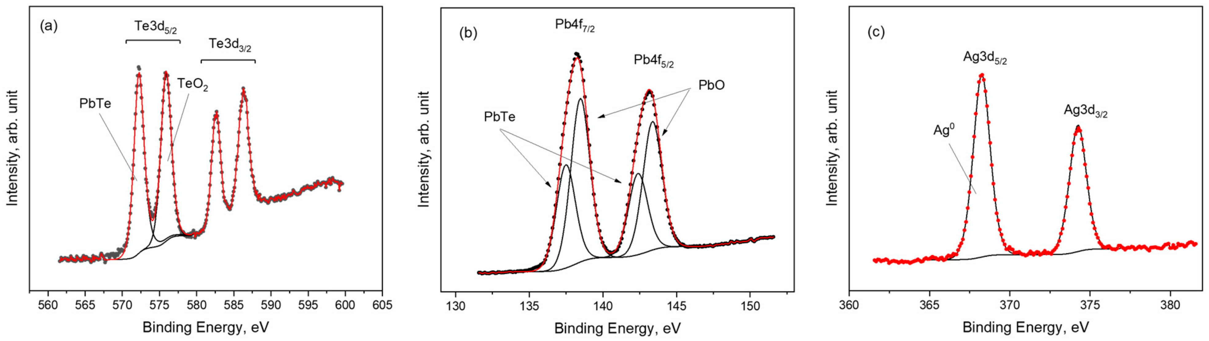
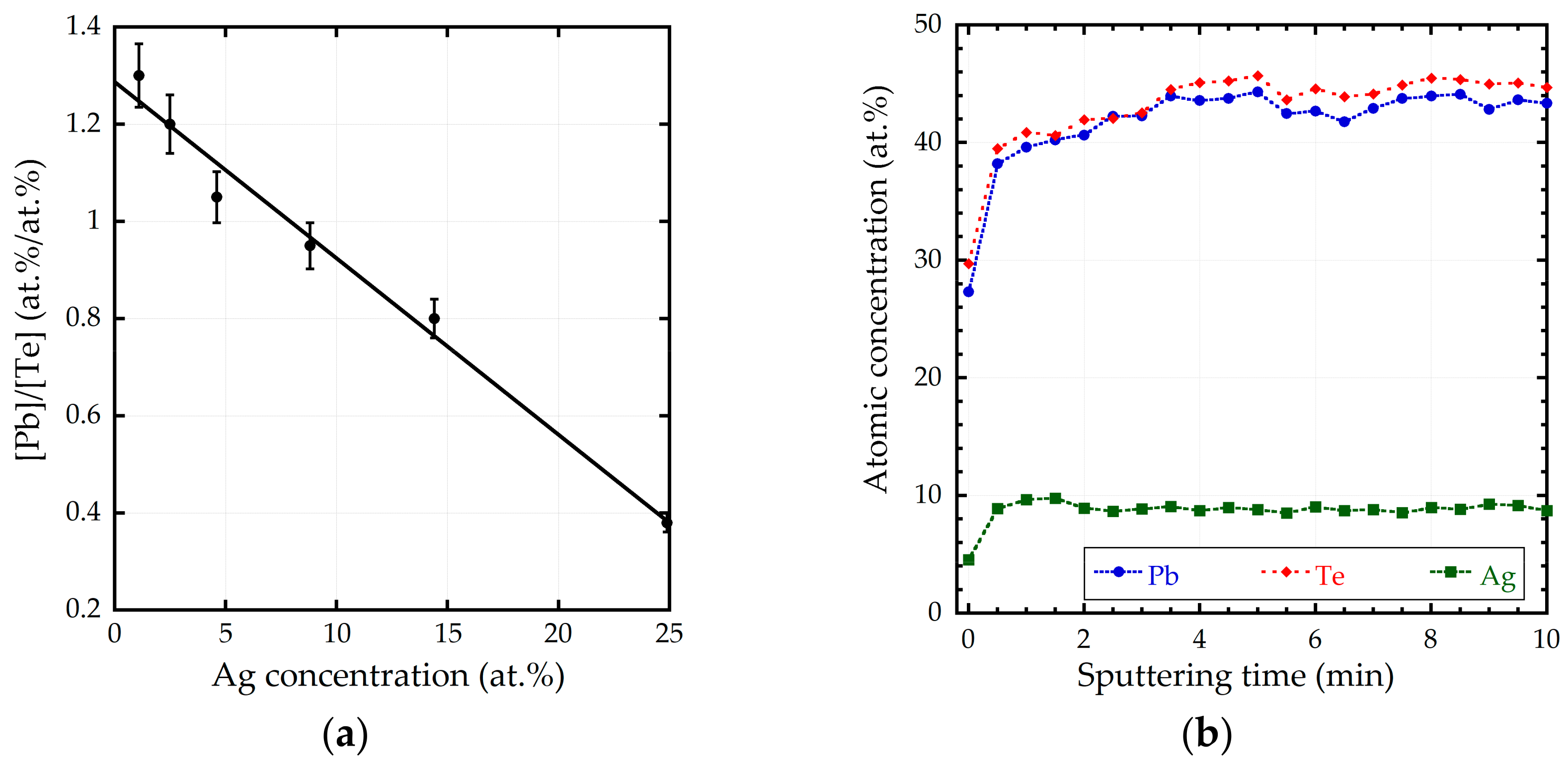
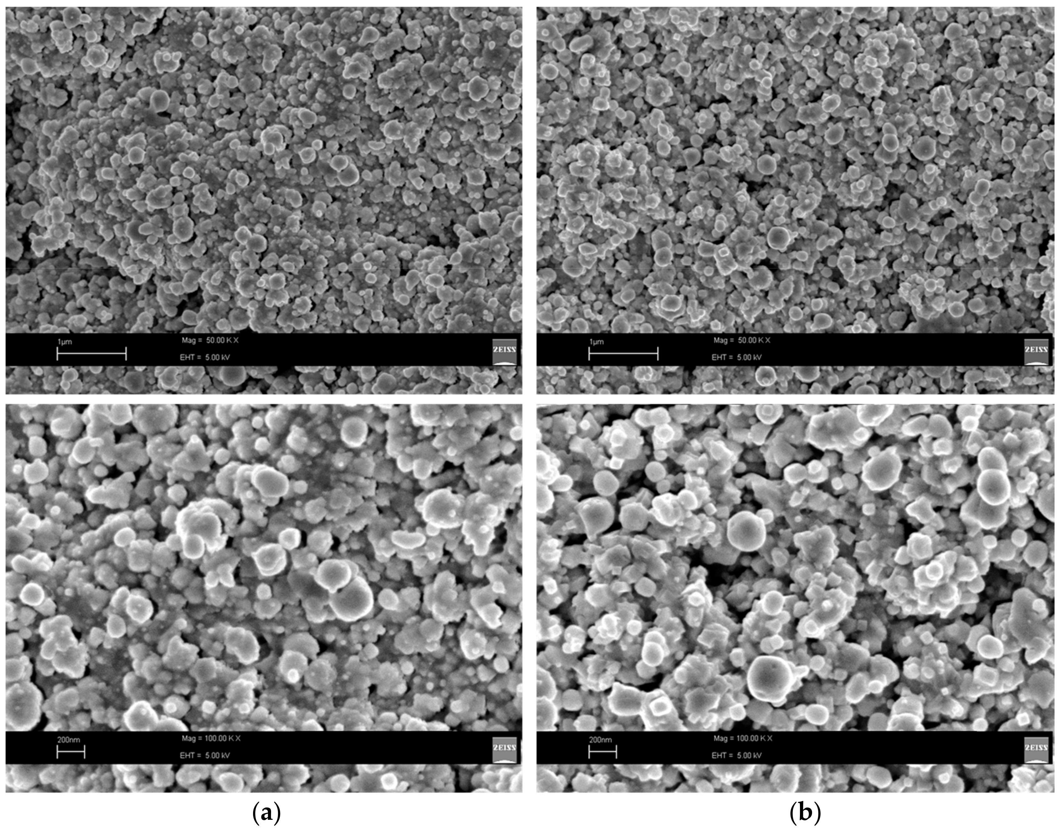
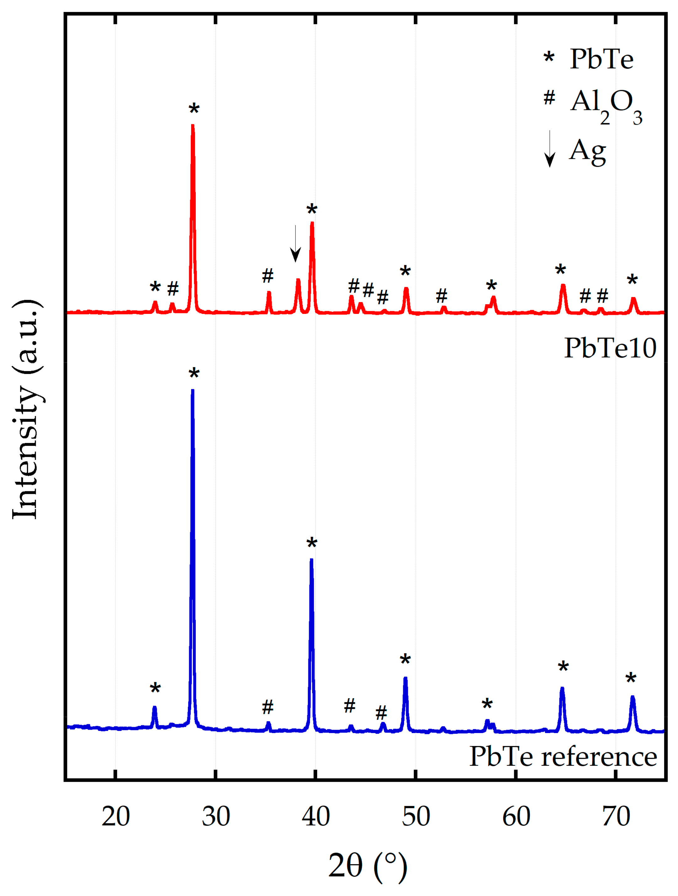
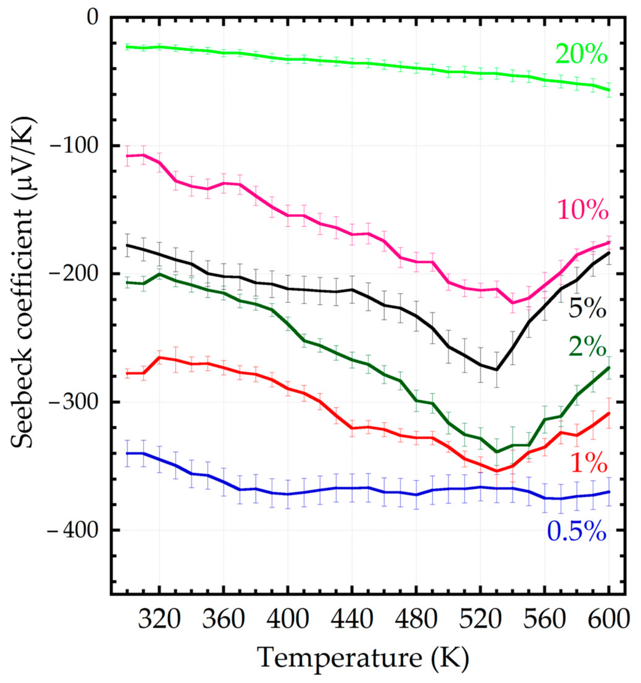
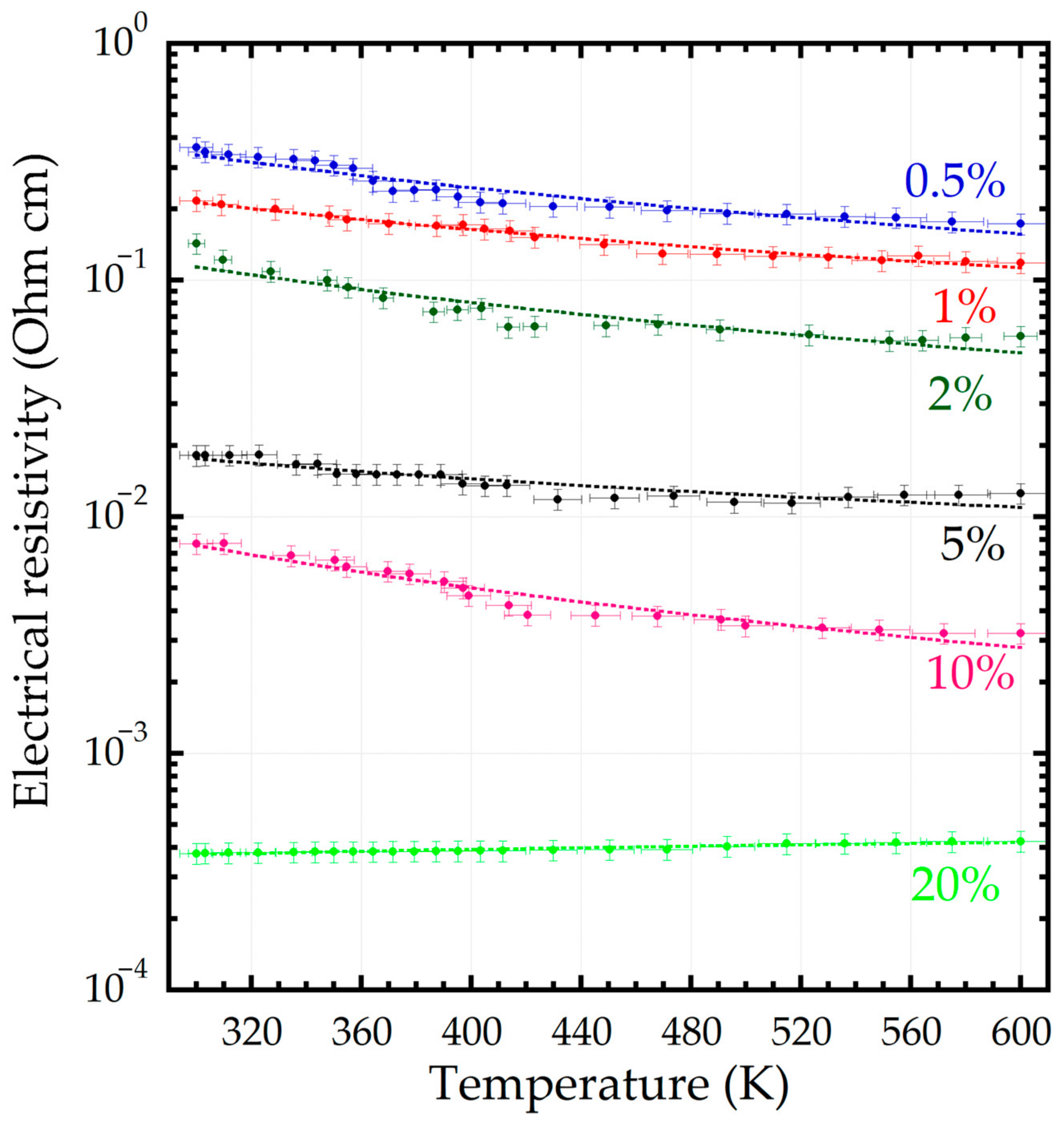
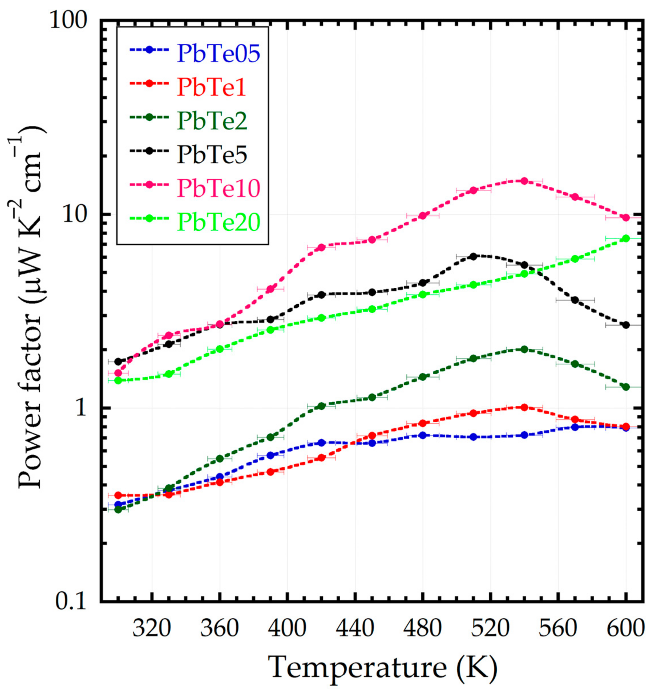
The experimental setup of the PLD system consists of an ultra-short Spectra Physics Spitfire Pro XP Ti:Sapphire pulsed laser source (wavelength λ = 800 nm, pulse duration of ~100 fs; energy of 3.7 ± 0.1 mJ/pulse) in front of a stainless steel vacuum chamber evacuated by a turbo molecular pump (typical background pressure of 5 × 10⁻⁷ mbar). The pulse repetition rate was fixed to 100 Hz (the maximum selectable value is 1 kHz). The PbTe and Ag targets (commercial 1-inch diameter targets, 99.999% purity) were placed on a rotating holder during ablation to avoid cratering. The laser beam was focused with an entrance angle of 45°, by a 1.0 m focal lens. As previously described [35,36], a multi-target system was used to deposit both materials through a PbTe/Ag multi-layered structure. The doping process was properly time-regulated and tuned to obtain a final product with specific Ag atomic percentage composition, promoting the Ag diffusion into the film. For the doping process, a PbTe/Ag multilayer structure was considered an acceptable attempt to reach a heavy doping condition. A doping sequence as N × (A(t1)∙B(t2)), with A = PbTe, B = Ag, and t1, t2, N as variable parameters according to the nominal Ag concentration, was used to perform the deposition. The overall deposition time was 30 min for all the samples. The growth rate was 0.11 μm/min, evaluated by ex-situ measurements of the film thickness. Technical-grade mirror-polished alumina plates were used as deposition substrates. All the substrates were ultrasonically cleaned in n-hexane and positioned on a sample holder maintained at room temperature at ~ 50 mm from the target.
XPS measurements were performed using an ESCALAB 250Xi spectrometer (Thermo Fisher Scientific Ltd., Basingstoke, UK), equipped with a monochromatic Al Kα source (1486.7 eV) for XPS and a six channeltrons detection system. The binding energy (BE) scale was calibrated, positioning the adventitious carbon peak C 1s at BE = 285.0 eV. The photoemission spectra were acquired at constant pass energy of 50 eV. The Avantage v.5.9 software (Thermo Fisher Scientific Ltd., Basingstoke, UK) was used to collect and process the spectra.
Surface morphology was characterized by a Field Emission Scanning Electron Microscopy apparatus (FE-SEM model Supra 40, ZEISS NTS Gmbh, Oberkochen, Germany), to be able to observe the grown materials at a very high resolution, down to nanometric sizes.
Grazing angle X-ray micro-diffraction (μ-XRD) measurements, which are typically used for investigating the structural parameters of surfaces different from the bulk and thin films [40], were performed using a Rigaku D/MAX RAPID (Tokyo, Japan) diffraction system, operating at 40 kV and 30 mA. This instrument is equipped with a Cu Kα source, curved-image plate detector, flat graphite monochromator, variety of beam collimators, and motorized stage (allowing two angular movements, rotation ϕ and revolution ω). The μ-XRD data were collected as two-dimensional images and then converted into Angle (2θ)−Intensity profiles using specific software provided by the producer. The data were acquired using 50 μm collimator, 1 h of collection time, a fixed revolution angle ω (3°), and rotation angles Φ (60°, 75°, 80°, 90°). The peak assignment was made using JCPDS database, whereas the unit-cell parameters of the PbTe samples were refined from the μ-XRD data using the UNITCELL software [41].
The temperature-dependent electrical characterization was performed in a homemade vacuum chamber by using the “four-contact-in-line-points probe” method. This method allows the measurement of sheet resistance under dark conditions and film resistivity when the thickness is known. Sheet resistance is commonly used to characterize thin film materials, with almost uniform thickness. The measurements were performed in a homemade system varying the temperature in the range of 300–600 K under controlled vacuum conditions (~10−3 mbar). The value of the film thickness used for the calculation of the electrical resistivity was 3.30 ± 0.05 μm, measured by a commercial profilometer and found almost constant for all the samples. The setup scheme and the details of the method are reported in a previous paper [42].
The Seebeck coefficient measurements were performed using commercial Seebeck Instruments K-20 and SB-100 (MMR technologies, San Jose, CA, USA) with a high impedance amplifier (30 gain) in the temperature range 300–600 K, following the method reported by Ko and Murray [43].

3. Results

The experiments reported in this article follow the work we have undertaken and published on the deposition of thermoelectric PbTe-based thin films via ns- and fs-PLD [35,36]. Our previous experiments verified some fundamental aspects concerning both the PLD methods with related advantages/limitations and some important properties of the materials themselves, which are usually prepared and studied in the form of bulk solid materials.
In particular, an ultrashort laser for PLD is preferred as an activating source if compared to more traditional ns-pulse laser for the following reasons: (i) the rate of ablation and subsequent growth of the film is much higher, and layers of micrometers can be obtained in few minutes; (ii) the material deposited is nanostructured, therefore perfectly functional to request a specific nano-sized structure; (iii) the stoichiometry of the target is maintained without any chemical disproportion; (iv) the material obtained resulted in being crystalline even by keeping the substrate at room temperature; and (v) the adopted multi-target and multi-layered deposition, which is time-regulated, can potentially give the required atomic composition, through the entire thickness of the film.
In the present experiments, we have grown room-temperature PbTe films with the addition of Ag by PLD, operated by an ultra-short fs laser beam, comparing the typical physical–chemical parameters (microstructural, stoichiometric, and electrical) of films at different nominal dopant concentrations, whose expected values were calculated as atomic percentages.
First, the surface chemical composition of the different samples was investigated by XPS analysis. The obtained results evidenced that PbTe films doped with different amounts of Ag were deposited. This result is confirmed by the peak-fitting analysis performed on the spectra shown in Figure 1, shown for PbTe10, as an example. The peaks of Te3d5/2 and Pb 4f7/2 positioned at BE = 137.5 eV and 572.2 eV, respectively, were assigned to PbTe. However, upon contact with air, a thin layer of oxides (few nm) is formed, as evidenced in the spectra deconvolution, which is then promptly removed after a few seconds of ion sputtering (Ar+—1 keV). Instead, the Ag spectrum was characterized by a single Ag3d5/2 peak positioned at 368.3 eV, BE value characteristic for Ag0, thus excluding the formation of secondary phases, such as Ag2Te [21].
Table 2 shows the main chemical information derived from the XPS investigation.
From the analysis of the XPS data, it is possible to state that the atomic [Ag] concentration is quite high with respect to the nominal one. This difference is higher when the nominal concentration is low because of the time-dependence of the multi-layer process: for low concentration, the time for a single step is lower and the error increases. However, a linear dependence between the [Pb]/[Te] atomic concentration ratio and the Ag atomic concentration was found (Figure 2a). The amount of Ag corresponding to a stoichiometry close to the correct one ([Pb]/[Te] = 1) is up to 8.8 at.%, whereas the ratio [Pb]/[Te] drastically decreases for [Ag] concentration >8.8 at.% when [Te] is much higher than [Pb]. The large difference from the correct stoichiometry with an excess of Te atoms is surely ascribable to the high number of Ag atoms, which can physically substitute Pb atoms in the Pb–Te system but can also produce doping in interstitial sites or by metallic aggregates. Figure 2b shows the depth profile of the sample PbTe05, which points out how the concentrations of Pb, Te and Ag are quite constant along the thickness of the film apart from the first surface layers (due to carbon and oxygen contaminations).
An evident and characteristic granular nanosized structure is clearly visible in micrographs obtained by SEM, as shown in Figure 3 for samples PbTe05 and PbTe20. The other samples show very similar morphologies and, for brevity, are not reported. An estimation of the size of the granules was carried out via open-source software for imaging analysis (ImageJ, National Institutes of Health, Bethesda, MD, USA) [44]. The size of the granules is randomly distributed from about 220 nm (constituted by few crystallites) down to approximately 30 nm (consisting of single crystallites).
In Figure 4, the XRD spectra of the undoped PbTe (altaite) and that of the sample PbTe10 are shown. We state that the films at different Ag compositions present the same features, without any significant variations in the position and intensity of the reflections reported for the sample PbTe10.
It is possible to state that the deposition at room temperature induces the formation of a poly crystalline PbTe film, characterized by the position of the main peaks extremely coherent with the altaite crystal shown in the undoped sample. The crystallite orientation is predominantly in the (200) plane of the cubic phase. All the samples with the Ag addition have a reflection at 2θ = 38.12°; this diffraction signal can be attributed to the reflection (111) of Ag nanoparticles [45]. Scherrer’s method [46] was applied to the full width at half maximum (FWHM) of the main peak (200) of the cubic PbTe to estimate the size of the crystalline grains. The values of grain size are shown in Table 3 and range from 25 to 39 nm, with a slight increase as a function of the Ag concentration. More interestingly, the extrapolation of the values of the lattice parameter evidences that there is a tendency for reduction when the Ag concentration increases. The decrease in the lattice constant is usually related to the formation of ternary compounds, such as Pb1−xAgxTe, with the Ag ionic radius being smaller than that of Pb [47]. However, since the lattice parameter does not follow an expected clear trend as a function of the Ag concentration (i.e., Vegard’s law), it is most probable that the presence of such compounds is only partially distributed, as reported elsewhere [31]. One of the possible explanations for such behavior is the low solubility limit of Ag for PbTe crystals [48].
From these results, obtained by means of a detailed μ-XRD analysis with a low grazing angle specific for thin film characterization, we can thus conclude that the films are characterized by a granular type of crystalline PbTe nanostructure, with the added Ag playing the role of dopant atoms in the PbTe lattice and creating some metallic dislocations among the grains. Most importantly, the specific particle sizes (25–39 nm) obtained are well befitting to fulfill the specific request for a good thermoelectric material of an effective scattering effect for thermal phonons, as requested to achieve a significant decrease in thermal conductivity inside the lattice of the material examined [7,10].
An analysis of the thermoelectric behavior was performed as a function of temperature in the range 300–600 K. Figure 5 shows the Seebeck coefficient (S) for the investigated samples, obtained from ten measurements performed consecutively after repeated heating/cooling cycles to also test the system repeatability (represented by the error bars in the figure). We found for all the samples a negative sign of S, indicating an n-type (electrons) conduction for the majority carriers. At the same time, the absolute value decreases as a function of the Ag concentration, with the sample PbTe20 showing a very low value of S, about one order of magnitude lower than PbTe05. This trend can be expected since the presence of the dopant should increase the carrier concentration. Indeed, according to the electron transport models that are typically used, i.e., the single parabolic band model, S depends on the carrier concentration, such that the lower the carrier concentration, the larger the Seebeck coefficient [7].
Conversely, the Seebeck coefficient shows a particular temperature dependence for all the samples, apart from PbTe05 and PbTe20, with a minimum value between 530 and 550 K. This behavior can be explained with a so-called dynamic doping process, which can occur due to the increase in the carrier concentration when the temperature increases [49]. This performance was fully demonstrated for the addition of Ag atoms in n-type PbTe, where silver compensates the Pb vacancies below 500 K and provides electrons in excess, occupying interstitial sites above 500 K, and thus increasing carrier concentration and/or mobilities [50].
Conversely, the higher nominal Ag concentration induces a lower electrical resistivity (ρ), as shown in Figure 6. The resistivity decreases as a function of the temperature, thus indicating a semiconducting behavior for all the samples apart from the sample PbTe20. The latter shows the electrical resistivity, which increases when the temperature increases, thus pointing out a behavior of a degenerate semiconductor assumed when the Ag concentration is higher than 20 at.%. Conversely to the Seebeck coefficient, we did not find any temperature-dependent change in the electrical resistivity, thus pointing out that future investigations must be conducted to highlight the complex mechanism of the doping needed to completely improve the electronic transport.
By combining the electrical conductivity σ = 1/ρ and the Seebeck coefficient measurements, it was finally possible to evaluate the material power factor, defined as PF = S2 × σ (Figure 7).
The PF increases as a function of the dopant concentration up to the nominal concentration of 10%, whereas the trend is opposite for the most doped sample PbTe20 due to the very low value of S. Note that the PF is larger by more than one order of magnitude for the sample PbT10 with respect to the PbTe05 one. It is interesting to state that, apart from PbTe05 and PbTe20, the samples show a maximum for PV ranging from 510 and 540 K, corresponding to the minimum observed for S, thus indicating a specific window for the upper temperature of the operations of a possible device. The highest PF value (14.9 μW K−2 cm−1 at 540 K) is more than four times the best performance of the PbTe films grown using ns-PLD by our group [35], thanks to a more efficient process of doping performed by the fs-PLD system. Generally, the results achieved in this study are in line with the PF values reported for thermoelectric films produced by magnetron-sputtering deposition (ranging from 0.33 to 23 μW K−2 cm−1) [51], and not far from complex nanocomposite PbTe-based bulk systems (up to 30 μW K−2 cm−1) [52].
The optimization of the power factor mainly depends on the best trade-off conditions between electrical conductivity and the Seebeck coefficient, which can be obtained with values of the carrier concentration (around 1020 cm−3) that are typical of highly doped semiconductors [7]. In our case in which Ag incorporation is applied, the best condition is achieved for a dopant concentration of [Ag] = 14.4 at.%. According to the results of this study, further optimization is difficult to obtain due to the excessive reduction in S if Ag concentration increases, regardless of the improvement in the electrical conductivity. However, co-doping with different elements or even with other complex alloys could be a strategy to be pursued to obtain thin films with improved performance.
To conclude the experimental activity, thermal annealing was performed to evaluate the stability of the thin films, which were left at 600 K for 72 h under vacuum conditions in the same setup used for the electrical resistivity measurements. Any significant change in the structural part of the film was observed, noting that even the electrical parameters did not show significant changes (<5% in terms of absolute value) following the thermal treatment. Therefore, it is possible to state that excellent nanostructured and nano-crystalline films are obtained even with easier depositions at RT. The overall system results are stable from a thermodynamic point of view (the grain structure remains unaltered); although, at present, we have no specific data about any change in the density of the films.

4. Discussion

The characterization of the Ag-added PbTe samples prepared in this work showed that nanostructured materials can be natively deposited by fs-PLD, with an average grain size significantly lower than 100 nm. The process of nanostructuring at dimensions smaller than the mean free path of phonons, while larger than those of charge carriers, allows us to obtain a material with good thermoelectric characteristics [6]. In these conditions, in fact, the phonons are scattered, reducing the lattice’s thermal conductivity, while the mobility of charge carriers and electron conduction can remain unchanged.
Therefore, fs-PLD is found to be a powerful technique for producing efficient thermoelectric thin films, combining native nanostructuring with the capability of growing films at RT and at a high deposition rate, as well as being able to dope the materials with the addition of different elements to the starting material structure.
To have an idea of the potential of the developed thin films, a possible estimation of zT can be carried out for the best-produced sample (PbTe10). A zT = 0.64 at the optimum temperature of 540 K is roughly estimated, considering κ ~ 1.25 × 10⁻² W cm−1 K−1 as an indicative value of thermal conductivity. This value of κ has been recently reported for a bulk PbTe:Ag system [50]. Furthermore, ultralow values of lattice thermal conductivity (κL) have been measured for specific PbTe-AgBiTe2 bulk alloys, equal to ~4.0 × 10⁻³ W cm−1 K−1, which is close to the glass theoretical limit for PbTe [53]. If we suppose achieving a similar reduction in κL and, taking into account the calculated electronic thermal conductivity κe = L × σ × T of 3.9 × 10⁻³ at T = 540 K for PbTe10 sample (by fixing L = 2.4 × 10⁻⁸ V2 K−2 [31]), a promising value of zT of 1.02 could be obtained for PbTe10.

5. Conclusions

The thermoelectric properties of PbTe thin films, deposited with various Ag concentrations by fs-PLD, were investigated to verify the effectiveness of Ag incorporation to enhance the power factor.
From a correlation between XPS and XRD analyses, we can conclude that the thin films are composed of nanostructured (25–39 nm) crystalline grains of PbTe, in which Ag atoms behave partially as effective dopant, by filling existing vacancies or substituting Pb atoms, and also create metallic nano-agglomerates along the grain dislocations.
Electrical resistivity measurements show the typical behavior of semiconductors, apart from the sample with the highest Ag concentration (24.9 at.%), which displays the behavior of a degenerate semiconductor, increasing the resistivity as a function of the temperature. As was predicted, the resistivity decreases significantly with the increasing atomic percentage of Ag. Regarding the Seebeck coefficient, the measurements point out that electrons are the majority carriers and the absolute value decreases as a function of the Ag concentration, thus indicating an increase in the carrier concentration when the quantity of Ag atoms increases. Interestingly, dynamic doping for the Ag-added PbTe system was identified, leading to a maximization of the performance in the range 510–540 K. Moreover, the material deposited at RT proved to be totally stable, both from a structural, morphological, and electrical point of view, after a thermal treatment for 72 h under the maximum investigated temperature (600 K), showing that this material can grow with excellent structure and properties even under experimental conditions that are very mild and accessible.
A maximum PF value of 14.9 μW K−2 cm−1 was recorded at 540 K for the sample with an Ag concentration of 14.4 at.%, improving the performance of the PbTe films obtained previously with deposition via both ns- and fs-PLD by our group. However, these values are still lower than the best results obtained by other approaches (in terms of both materials and techniques) and, above all, by bulky solutions. Therefore, other strategies, including co-doping with different elements or even complex alloys, should be considered for achieving a further improvement of the thermoelectric properties.
Finally, we can conclude that the deposition method of fs-PLD has proven to be extremely advantageous, both as regards the high growth rate (i.e., 110 nm/min), both for obtaining crystalline material of cubic PbTe with silver incorporation, even at room temperature, and for the unique characteristic of giving rise to nano-sized granular structures in the range 25–200 nm, as demonstrated by detailed structural and morphological investigations. In the future, measurements of thermal conductivity will be performed to measure the effective zT of the produced thin films.

Author Contributions

A.B.: conceptualization, methodology, investigation, data curation, visualization, writing—original draft preparation; S.O.: methodology; L.M., A.L., A.M. and S.K.: investigation; D.M.T.: conceptualization, validation, writing—review and editing, supervision. All authors have read and agreed to the published version of the manuscript.

Funding

This research received no external funding.

Data Availability Statement

Not applicable.

Acknowledgments

The authors thank Emilia Cappelli for her initial contribution to this work.

Conflicts of Interest

The authors declare no conflict of interest.

References

  1. Champier, D. Thermoelectric generators: A review of applications. Energy Convers. Manag. 2017, 140, 167–181. [Google Scholar] [CrossRef]
  2. Tritt, T.M.; Subramanian, M.A. Thermoelectric Materials, Phenomena, and Applications: A Bird’s Eye View. MRS Bull. 2006, 31, 188–198. [Google Scholar] [CrossRef] [Green Version]
  3. Baranowski, L.L.; Snyder, G.J.; Toberer, E.S. Concentrated solar thermoelectric generators. Energy Environ. Sci. 2012, 5, 9055. [Google Scholar] [CrossRef] [Green Version]
  4. Trucchi, D.M.; Bellucci, A.; Girolami, M.; Calvani, P.; Cappelli, E.; Orlando, S.; Polini, R.; Silvestroni, L.; Sciti, D.; Kribus, A. Solar Thermionic-Thermoelectric Generator (ST2G): Concept, Materials Engineering, and Prototype Demonstration. Adv. Energy Mater. 2018, 8, 1802310. [Google Scholar] [CrossRef]
  5. Bellucci, A.; Girolami, M.; Mastellone, M.; Serpente, V.; Trucchi, D.M. Upgrade and present limitations of solar thermionic-thermoelectric technology up to 1000 K. Sol. Energy Mater. Sol. Cells 2021, 223, 110982. [Google Scholar] [CrossRef]
  6. Dresselhaus, M.S.; Chen, G.; Tang, M.Y.; Yang, R.G.; Lee, H.; Wang, D.Z.; Ren, Z.F.; Fleurial, J.P.; Gogna, P. New Directions for Low-Dimensional Thermoelectric Materials. Adv. Mater. 2007, 19, 1043–1053. [Google Scholar] [CrossRef]
  7. Snyder, G.J.; Toberer, E.S. Complex thermoelectric materials. Nat. Mater. 2008, 7, 105–114. [Google Scholar] [CrossRef] [Green Version]
  8. Kanatzidis, M.G. Nanostructured Thermoelectrics: The New Paradigm? Chem. Mater. 2010, 22, 648–659. [Google Scholar] [CrossRef]
  9. Venkatasubramanian, R.; Silvola, E.; Colpitts, T.; O’Quinn, B. Thin-film thermoelectric devices with high room-temperature figures of merit. Nature 2001, 413, 597–602. [Google Scholar] [CrossRef]
  10. Biswas, K.; He, J.; Blum, I.D.; Wu, C.I.; Hogan, T.P.; Seidman, D.N.; Dravid, V.P.; Kanatzidis, M.G. High-performance bulk thermoelectrics with all-scale hierarchical architectures. Nature 2012, 489, 414–418. [Google Scholar] [CrossRef]
  11. Yang, L.; Chen, Z.-G.; Han, G.; Hong, M.; Zou, Y.; Zou, J. High-performance thermoelectric Cu2Se nanoplates through nanostructure engineering. Nano Energy 2015, 16, 367–374. [Google Scholar] [CrossRef]
  12. Zhang, Y.; Mehta, R.J.; Belley, M.; Han, L.; Ramanath, G.; Borca-Tasciuc, T. Lattice thermal conductivity diminution and high thermoelectric power factor retention in nanoporous macroassemblies of sulfur-doped bismuth telluride nanocrystals. Appl. Phys. Lett. 2012, 100, 193113. [Google Scholar] [CrossRef]
  13. Chowdhury, I.; Prasher, R.; Lofgreen, K.; Chrysler, G.; Narasimhan, S.; Mahajan, R.; Koester, D.; Alley, R.; Venkatasubramanian, R. On-chip cooling by superlattice-based thin-film thermoelectrics. Nat. Nanotechnol. 2009, 4, 235–238. [Google Scholar] [CrossRef]
  14. Elyamny, S.; Dimaggio, E.; Magagna, S.; Narducci, D.; Pennelli, G. High Power Thermoelectric Generator Based on Vertical Silicon Nanowires. Nano Lett. 2020, 20, 4748–4753. [Google Scholar] [CrossRef]
  15. Blackburn, J.L.; Ferguson, A.J.; Cho, C.; Grunlan, J.C. Carbon-Nanotube-Based Thermoelectric Materials and Devices. Adv. Mater. 2018, 30, 1704386. [Google Scholar] [CrossRef]
  16. Li, X.; Cai, K.; Gao, M.; Du, Y.; Shen, S. Recent advances in flexible thermoelectric films and devices. Nano Energy 2021, 89, 106309. [Google Scholar] [CrossRef]
  17. Xie, H.; Zhang, Y.; Gao, P. Thermoelectric-Powered Sensors for Internet of Things. Micromachines 2022, 14, 31. [Google Scholar] [CrossRef]
  18. Han, C.; Tan, G.; Varghese, T.; Kanatzidis, M.G.; Zhang, Y. High-Performance PbTe Thermoelectric Films by Scalable and Low-Cost Printing. ACS Energy Lett. 2018, 3, 818–822. [Google Scholar] [CrossRef]
  19. Fan, P.; Fan, W.-F.; Zheng, Z.-H.; Zhang, Y.; Luo, J.-T.; Liang, G.-X.; Zhang, D.-P. Thermoelectric properties of zinc antimonide thin film deposited on flexible polyimide substrate by RF magnetron sputtering. J. Mater. Sci. Mater. Electron. 2014, 25, 5060–5065. [Google Scholar] [CrossRef]
  20. Symeou, E.; Pervolaraki, M.; Mihailescu, C.N.; Athanasopoulos, G.I.; Papageorgiou, C.; Kyratsi, T.; Giapintzakis, J. Thermoelectric properties of Bi0.5Sb1.5Te3 thin films grown by pulsed laser deposition. Appl. Surf. Sci. 2015, 336, 138–142. [Google Scholar] [CrossRef]
  21. Bala, M.; Gupta, S.; Tripathi, T.S.; Varma, S.; Tripathi, S.K.; Asokan, K.; Avasthi, D.K. Enhancement of thermoelectric power of PbTe: Ag nanocomposite thin films. RSC Adv. 2015, 5, 25887–25895. [Google Scholar] [CrossRef]
  22. Bellucci, A.; Mastellone, M.; Girolami, M.; Orlando, S.; Medici, L.; Mezzi, A.; Kaciulis, S.; Polini, R.; Trucchi, D.M. ZnSb-based thin films prepared by ns-PLD for thermoelectric applications. Appl. Surf. Sci. 2017, 418, 589–593. [Google Scholar] [CrossRef]
  23. Xu, S.; Zhu, W.; Zhao, H.; Xu, L.; Sheng, P.; Zhao, G.; Deng, Y. Enhanced thermoelectric performance of SnTe thin film through designing oriented nanopillar structure. J. Alloys Compd. 2018, 737, 167–173. [Google Scholar] [CrossRef]
  24. Wang, A.; Xue, Y.; Wang, J.; Yang, X.; Wang, J.; Li, Z.; Wang, S. High thermoelectric performance of Cu2Se-based thin films with adjustable element ratios by pulsed laser deposition. Mater. Today Energy 2022, 24, 100929. [Google Scholar] [CrossRef]
  25. Wei, M.; Ma, H.L.; Nie, M.Y.; Li, Y.Z.; Zheng, Z.H.; Zhang, X.H.; Fan, P. Enhanced Thermoelectric Performance of CoSb3 Thin Films by Ag and Ti Co-Doping. Materials 2023, 16, 1271. [Google Scholar] [CrossRef]
  26. Thaowonkaew, S.; Insawang, M.; Vora-ud, A.; Horprathum, M.; Muthitamongkol, P.; Maensiri, S.; Kumar, M.; Phan, T.B.; Seetawan, T. Effect of substrate rotation and rapid thermal annealing on thermoelectric properties of Ag-doped Sb2Te3 thin films. Vacuum 2023, 211, 111920. [Google Scholar] [CrossRef]
  27. Latronico, G.; Mele, P.; Sekine, C.; Wei, P.S.; Singh, S.; Takeuchi, T.; Bourges, C.; Baba, T.; Mori, T.; Manfrinetti, P.; et al. Effect of the annealing treatment on structural and transport properties of thermoelectric Smy(FexNi1−x)4Sb12 thin films. Nanotechnology 2023, 34, 115705. [Google Scholar] [CrossRef]
  28. Dughaish, Z.H. Lead telluride as a thermoelectric material for thermoelectric power generation. Phys. B Condens. Matter 2002, 322, 205–223. [Google Scholar] [CrossRef]
  29. Pei, Y.; Wang, H.; Snyder, G.J. Band Engineering of Thermoelectric Materials. Adv. Mater. 2012, 24, 6125–6135. [Google Scholar] [CrossRef]
  30. Takagiwa, Y.; Pei, Y.; Pomrehn, G.; Snyder, G.J. Dopants effect on the band structure of PbTe thermoelectric material. Appl. Phys. Lett. 2012, 101, 092102. [Google Scholar] [CrossRef] [Green Version]
  31. Dow, H.S.; Oh, M.W.; Kim, B.S.; Park, S.D.; Min, B.K.; Lee, H.W.; Wee, D.M. Effect of Ag or Sb addition on the thermoelectric properties of PbTe. J. Appl. Phys. 2010, 108, 113709. [Google Scholar] [CrossRef]
  32. Ito, M.; Seo, W.-S.; Koumoto, K. Thermoelectric properties of PbTe thin films prepared by gas evaporation method. J. Mater. Res. 1999, 14, 209–212. [Google Scholar] [CrossRef]
  33. Shing, Y.H.; Chang, Y.; Mirshafii, A.; Hayashi, L.; Roberts, S.S.; Josefowicz, J.Y.; Tran, N. Sputtered Bi2Te3 and PbTe thin films. J. Vac. Sci. Technol. A 1983, 1, 503–506. [Google Scholar] [CrossRef]
  34. Dauscher, A.; Dinescu, M.; Boffoué, O.M.; Jacquot, A.; Lenoir, B. Temperature-dependant growth of PbTe pulsed laser deposited films on various substrates. Thin Solid Film. 2006, 497, 170–176. [Google Scholar] [CrossRef]
  35. Cappelli, E.; Bellucci, A.; Medici, L.; Mezzi, A.; Kaciulis, S.; Fumagalli, F.; Di Fonzo, F.; Trucchi, D.M. Nano-crystalline Ag–PbTe thermoelectric thin films by a multi-target PLD system. Appl. Surf. Sci. 2014, 336, 283–289. [Google Scholar] [CrossRef]
  36. Bellucci, A.; Cappelli, E.; Orlando, S.; Medici, L.; Mezzi, A.; Kaciulis, S.; Polini, R.; Trucchi, D.M. Fs-pulsed laser deposition of PbTe and PbTe/Ag thermoelectric thin films. Appl. Phys. A Mater. Sci. Process. 2014, 117, 401–407. [Google Scholar] [CrossRef] [Green Version]
  37. Amoruso, S.; Ausanio, G.; Bruzzese, R.; Lanotte, L.; Scardi, P.; Vitiello, M.; Wang, X.T. Synthesis of nanocrystal films via femtosecond laser ablation in vacuum. J. Phys. Condens. Matter 2006, 18, L49–L53. [Google Scholar] [CrossRef]
  38. Bellucci, A.; Orlando, S.; Girolami, M.; Mastellone, M.; Serpente, V.; Paci, B.; Generosi, A.; Mezzi, A.; Kaciulis, S.; Polini, R.; et al. Aluminum (Oxy)nitride thin films grown by fs-PLD as electron emitters for thermionic applications. AIP Conf. Proc. 2021, 2416, 020004. [Google Scholar] [CrossRef]
  39. Qiu, B.; Bao, H.; Zhang, G.; Wu, Y.; Ruan, X. Molecular dynamics simulations of lattice thermal conductivity and spectral phonon mean free path of PbTe: Bulk and nanostructures. Comput. Mater. Sci. 2012, 53, 278–285. [Google Scholar] [CrossRef]
  40. Sakata, O.; Nakamura, M. Grazing Incidence X-Ray Diffraction. In Surface Science Techniques; Bracco, G., Holst, B., Eds.; Springer: Berlin/Heidelberg, Germany, 2013; pp. 165–190. [Google Scholar]
  41. Holland, T.J.B.; Redfern, S.A.T. UNITCELL: A nonlinear least-squares program for cell-parameter refinement and implementing regression and deletion diagnostics. J. Appl. Crystallogr. 1997, 30, 84. [Google Scholar] [CrossRef] [Green Version]
  42. Trucchi, D.M.; Zanza, A.; Bellucci, A.; Marotta, V.; Orlando, S. Photoconductive and photovoltaic evaluation of In2O3–SnO2 multilayered thin-films deposited on silicon by reactive pulsed laser ablation. Thin Solid Film. 2010, 518, 4738–4742. [Google Scholar] [CrossRef]
  43. Ko, D.K.; Murray, C.B. Probing the Fermi Energy Level and the Density of States Distribution in PbTe Nanocrystal (Quantum Dot) Solids by Temperature-Dependent Thermopower Measurements. ACS Nano 2011, 5, 4810–4817. [Google Scholar] [CrossRef] [PubMed]
  44. Schneider, C.A.; Rasband, W.S.; Eliceiri, K.W. NIH Image to ImageJ: 25 years of image analysis. Nat. Methods 2012, 9, 671–675. [Google Scholar] [CrossRef] [PubMed]
  45. Swetha, V.; Lavanya, S.; Sabeena, G.; Pushpalaksmi, E.; Jenson, S.J.; Annadurai, G. Synthesis and Characterization of Silver Nanoparticles from Ashyranthus aspera Extract for Antimicrobial Activity Studies. J. Appl. Sci. Environ. Manag. 2020, 24, 1161–1167. [Google Scholar] [CrossRef]
  46. Jagodzinski, H.; Klug, H.P.; Alexander, L.E. X-ray Diffraction Procedures for Polycrystalline and Amorphous Materials, 2. Auflage. John Wiley & Sons, New York-Sydney-Toronto 1974, 966 Seiten, Preis: £18.55. Ber. Bunsenges. Phys. Chem. 1975, 79, 553. [Google Scholar]
  47. Miotkowska, S.; Dynowska, E.; Miotkowski, I.; Szczerbakow, A.; Witkowska, B.; Kachniarz, J.; Paszkowicz, W. The lattice constants of ternary and quaternary alloys in the PbTe–SnTe–MnTe system. J. Cryst. Growth 1999, 200, 483–489. [Google Scholar] [CrossRef]
  48. Sharov, M.K. Silver solubility in PbTe crystals. Inorg. Mater. 2008, 44, 569–571. [Google Scholar] [CrossRef]
  49. Pei, Y.; May, A.F.; Snyder, G.J. Self-Tuning the Carrier Concentration of PbTe/Ag2Te Composites with Excess Ag for High Thermoelectric Performance. Adv. Energy Mater. 2011, 1, 291–296. [Google Scholar] [CrossRef]
  50. Wang, S.; Chang, C.; Bai, S.; Qin, B.; Zhu, Y.; Zhan, S.; Zheng, J.; Tang, S.; Zhao, L.D. Fine Tuning of Defects Enables High Carrier Mobility and Enhanced Thermoelectric Performance of n-Type PbTe. Chem. Mater. 2023, 35, 755–763. [Google Scholar] [CrossRef]
  51. Zhang, Z.; Gurtaran, M.; Li, X.; Un, H.I.; Qin, Y.; Dong, H. Characterization of Magnetron Sputtered BiTe-Based Thermoelectric Thin Films. Nanomaterials 2023, 13, 208. [Google Scholar] [CrossRef]
  52. Rogacheva, E.I.; Krivulkin, I.M.; Nashchekina, O.N.; Sipatov, A.Y.; Volobuev, V.A.; Dresselhaus, M.S. Percolation transition of thermoelectric properties in PbTe thin films. Appl. Phys. Lett. 2001, 78, 3238–3240. [Google Scholar] [CrossRef]
  53. Zhu, H.; Zhang, B.; Zhao, T.; Zheng, S.; Wang, G.; Wang, G.; Lu, X.; Zhou, X. Achieving glass-like lattice thermal conductivity in PbTe by AgBiTe2 alloying. Appl. Phys. Lett. 2022, 121, 241903. [Google Scholar] [CrossRef]
Figure 1. Te3d (a), Pb4f (b), and Ag3d (c) spectra acquired by the investigation of the sample PbTe10.
Energies 16 03216 g001
Figure 2. (a) [Pb]/[Te] atomic concentration ratio as a function of the Ag concentration; (b) XPS depth profile for the sample PbTe05.
Energies 16 03216 g002
Figure 3. FE-SEM secondary electrons images of thin films: (a) PbTe05 and (b) PbTe20 at different magnifications. The nanostructured morphology of PbTe grains (~30 to 220 nm) is evident.
Energies 16 03216 g003
Figure 4. μ-XRD patterns taken at grazing incidence angle of the undoped PbTe, used as a reference, and the sample PbTe10.
Energies 16 03216 g004
Figure 5. Seebeck coefficient values as a function of the temperature.
Energies 16 03216 g005
Figure 6. Electrical resistivity values as a function of the temperature.
Energies 16 03216 g006
Figure 7. Power factor values as a function of the temperature.
Energies 16 03216 g007
Table 1. List of the most recent published works related to the production of thermoelectric nanostructured thin films, displaying material and dopants, technique, power factor at the temperature T, which maximizes the value, and year of publication.
Material/DopantsProduction TechniqueMaximum Power Factor
(W m−1 K−2) at T
Publication Year
(Reference)
ZnSbRF Magnetron Sputtering2.35 × 10−3 at 533 K2014 [19]
Bi0.5Sb1.5Te3KrF excimer PLD3.2 × 10−3 at 390 K2015 [20]
PbTeThermal evaporation~0.45 × 10⁻³ at 400 K2015 [21]
ZnSb/CrArF excimer PLD0.2 × 10−3 at 600 K2017 [22]
SnTeThermal evaporation1.98 × 10−3 at 823 K2018 [23]
Cu2SeXeCl excimer PLD~0.2 × 10⁻³ at 580 K2022 [24]
CoSb3/Ag, TiMagnetron Sputtering0.31 × 10−3 at 623 K2023 [25]
Sb2Te3/AgRF Magnetron Sputtering4.6 × 10−3 at 373 K2023 [26]
Smy(FexNi1−x)Sb12Nd: YAG PLD~0.38 × 10⁻³ at 525 K2023 [27]
Table 2. Values of the XPS atomic concentration of Ag and Pb/Te atomic ratio for the investigated samples.
Sample NameNominal [Ag] (%)[Ag] (at.%) 1[Pb]/[Te] (at.%/at.%) 1
PbTe050.51.11.2
PbTe112.51.2
PbTe224.61.1
PbTe558.80.9
PbTe101014.40.7
PbTe202024.90.4
1 Values measured after the sputtering of the first layers to remove contaminants.
Table 3. Values of lattice parameter and grain size derived from XRD data for each sample. The parentheses number represents the measurement accuracy.
Sample NameLattice Parameter (Å)Grain Size (nm)
PbTe056.454 (3)25
PbTe16.454 (4)25
PbTe26.453 (3)29
PbTe56.449 (3)39
PbTe106.447 (3)39
PbTe206.447 (3)39
Disclaimer/Publisher’s Note: The statements, opinions and data contained in all publications are solely those of the individual author(s) and contributor(s) and not of MDPI and/or the editor(s). MDPI and/or the editor(s) disclaim responsibility for any injury to people or property resulting from any ideas, methods, instructions or products referred to in the content.

