1. Introduction
Modern electric drives, particularly those powering AC machines, extensively deploy voltage-source inverters (VSIs) and various pulse-width modulation (PWM) techniques. The pursuit of minimizing current ripple and torque ripple, often achieved through higher carrier wave frequencies, introduces the challenge of significant switching losses in VSIs equipped with traditional silicon-based switching devices [
1]. To address this issue, wide-bandgap transistors such as gallium nitride (GaN) and silicon carbide (SiC) are increasingly employed [
2,
3], alongside innovative modulation strategies aimed at mitigating converter losses [
4,
5,
6]. These modern semiconductor devices offer switching frequencies several times higher than traditional silicon devices when comparable power is considered, making the inverters more compact due to the reduced volume of energy-accumulating components [
7]. Another benefit is the smoothed machine current, and consequently, torque, particularly relevant for machines with small inductances [
8]. However, increasing the switching frequencies raises switching losses and introduces the problem of electromagnetic compatibility (EMC) [
9].
In the context of modern electric vehicles and aircraft, crucial aspects include battery voltage utilization, overall drive efficiency, fault-tolerant operation, and the volume and weight of the converter [
10,
11,
12]. For these means of transport, the dual-inverter topology (DI), as proposed by Stemmler and Guggenbach [
13], emerges as a viable option due to its superior DC-bus voltage utilization and fault-tolerance capabilities [
14,
15]. It enables multilevel operation while keeping the converter structure relatively simple compared to full multilevel counterparts [
16,
17]. Of course, the trade-off involves doubling the number of semiconductor components and DC-link capacitors. However, the size of the capacitors can be optimized by selecting higher switching frequencies. Overall, this topology offers a promising landscape for advancing research, particularly in the field of modulation strategy optimization.
Three fundamental DI configurations—common direct current (DC) source type, isolated DC source type, and floating capacitor type—emerge, each with its set of advantages and challenges [
18]. While the common DC source type is compact and cost-effective, it may introduce zero-sequence current (ZSC), impacting the drive performance. Consequently, strategies to eliminate ZSC have been proposed in the literature, showcasing the complexity of this configuration [
19,
20,
21,
22,
23]. On the other hand, the floating capacitor configuration, though eliminating ZSC, exhibits limited fault-tolerance capabilities [
24,
25].
The DI topology with an isolated DC source, preventing ZSC circulation, strikes a balance between hardware complexity and efficiency. Although this configuration demands two separate DC power supplies, resulting in increased hardware size and cost. These disadvantages are partly offset by the availability of various control strategies [
26,
27,
28] achieving improved efficiency and reliability [
29]. Notably, in battery-powered drives, galvanic isolation can be achieved relatively easily by sorting the batteries into two groups with the same voltages [
11,
30].
Despite the potential benefits of DI systems, the utilization of twice as many switches compared to single VSIs raises concerns about increased conduction and switching losses. Various control strategies have been proposed to address these challenges [
31,
32,
33], involving sophisticated methods such as unified Space Vector Pulse Width Modulation (SVPWM) and clamping modulation techniques [
34]. Approaches outlined in [
32,
33,
35] involve clamping a specific number of legs in both inverters, aiming to decrease switching losses. These modern and computationally challenging methods involve dividing the voltage space vector plane into specific regions. Based on the position of the reference voltage vector, specific combinations of voltage vectors from both converters are switched accordingly.
This paper aims to present a simple and convenient way of effectively cutting off inverter losses by modifying well-known and conventional approaches. The DI inverter topology offers a high degree of freedom in distributing the reference voltage vector coming, for instance, from the motor control algorithm. Conventionally, the reference voltage vector is divided in the ratio 1:1 between the two converters [
18]. However, when the reference voltage vector is below 50% of the maximum voltage, it is beneficial to synthesize this vector using only one inverter while the other essentially creates a neutral point for the winding. Then, when the first inverter reaches its maximum in its linear modulation mode, the second inverter gradually starts to contribute to the voltage generation. In this way, switching losses can be optimized. It is important, however, to acknowledge that such an operation where only a single inverter is modulated results in an asymmetrical load distribution between the inverters. Consequently, the modulated inverter might experience accelerated aging and component degradation. This can be addressed by alternating between the inverters responsible for creating the neutral point. The switching can occur at any time as long as continuity of the fundamental voltage component is ensured, conveniently at integer multiples of the fundamental electric cycle.
Furthermore, it will also be shown that additional optimization of converter losses can be achieved solely by the selection of a modulation strategy. Arguably, one of the most prevalent asynchronous modulation strategies is the SVPWM. However, due to the bus-clamping feature of the so-called discontinuous PWM strategies (DPWM) belonging to the same carrier-based modulations as SVPWM, these strategies can yield lower switching losses since one of the inverter legs is clamped to either the negative or positive bus during the whole period [
34]. Probably the most popular DPWM strategy is the 60° or Depenbrock’s DPWM, commonly denoted DPWM1 [
34,
36].
Typically, traction AC electric drives are operated in such a way that it is desired to maintain constant (and maximum) torque up to the base speed when the field-weakening takes over. If the machine, either synchronous or induction, is controlled by the commonly utilized Field-Oriented Control (FOC), the constant (and nominal) torque operation implies a constant AC value of the current drawn from the source. Therefore, this paper proposes a reduction of losses via an asymmetrical control of the DI when a single inverter realizes the reference voltage vector up to 50% of the maximum voltage, from which the other inverter starts to contribute gradually. Also, it proposes using the DPWM1 carrier-based modulation strategy since it appears to be superior to the SVPWM within the DI topology. The advantages appear to be distinct in the considered topology since the DPWM1 decreases the switching losses and significantly improves the voltage waveform, yielding lower current and torque ripple due to its bus-clamping features.
Nowadays, simulation tools play a crucial role in the design of power converters and electric drives, and in the overall concept verification, the presented results are based on an extensive and detailed model in MATLAB/Simulink. It is shown that manufacturer-specific switching devices can be rigorously parameterized for loss calculation while keeping the switching nature of the semiconductor switch “ideal”, significantly optimizing the simulation time. Since it is necessary to assess the losses in as many operation points as possible while exploring the different features of modulation methods, the simulations leverage the parallel toolbox. The DI then supplies a 12 kW squirrel cage induction machine (IM) in an FOC loop parameterized based on real measurements.
Furthermore, another merit of the simulation setup is that it is possible to conveniently maintain the same current in terms of its RMS value and overall power factor at different mechanical operating points corresponding to various drive speeds. Maintaining identical conditions on a real drive poses challenges due to the dynamic changes in inverter and motor parameters with temperature, magnetic circuit saturation, or additional losses. Additionally, utilizing the approach presented in the following sections allows for the convenient separation of conduction and switching losses, enabling an assessment of their effects. This capability directly demonstrates the switching loss optimization—the key feature of the proposed method.
The structure of the paper is as follows:
Section 2 provides a brief overview of the DI topology, emphasizing modulation.
Section 3 introduces the proposed asymmetrical reference voltage distribution scheme. Finally,
Section 4 presents extensive simulation results, validating the proposed strategy and analyzing the effectiveness of different modulation strategies.
2. Utilized Topology
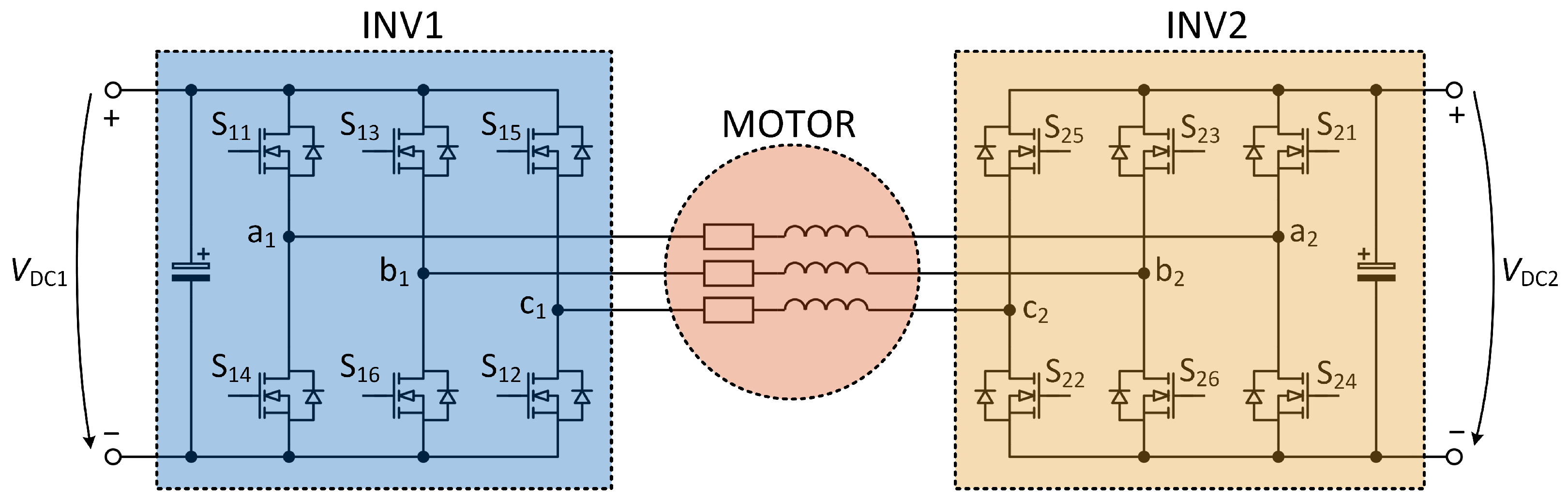
Thanks to its inherent advantage of eliminating the ZSC path and offering greater freedom in terms of possible modulation techniques, this paper investigates the dual-inverter topology with isolated DC-links.The topology is depicted in
Figure 1. The load, typically a stator winding of an AC machine, is connected between the two inverters. Crucially, each inverter is fed by a separate DC source, which must be galvanically isolated from one another to break the ZSC path. Consequently, all possible switching combinations can be used.
In principle, the DC-link voltage ratio can be set arbitrarily, yet the most common choice is to use equal DC-link voltages, i.e.,
. Furthermore, to simplify the notation and make expressions more coherent, we define a combined DC-link voltage as
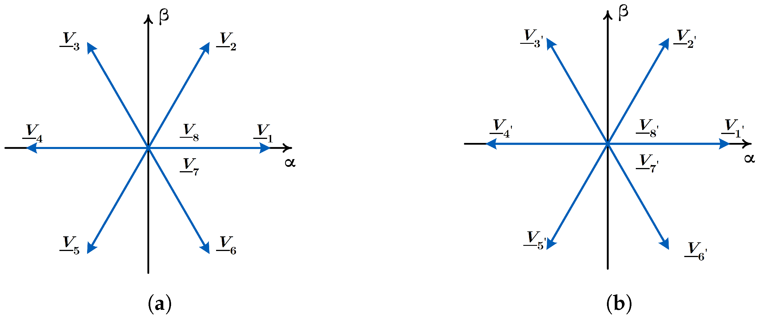
Consequently, both inverters generate identical fundamental voltage vectors. A conventional two-level voltage source inverter can assume eight different switching combinations, resulting in six active vectors and two zero vectors; see
Figure 2. The vectors are denoted
and
for INV1 and INV2, respectively.
The fundamental voltage vectors of each inverter can be written as
where
and
are the pole voltages of INV1 and INV2, respectively, and
. Moreover, the load-phase voltages (see
Figure 1) can be expressed as
Examining (
2) and (
3) yields that the resulting voltage vector of the dual-inverter topology can be obtained by simply subtracting the voltage vectors of both inverters, i.e.,
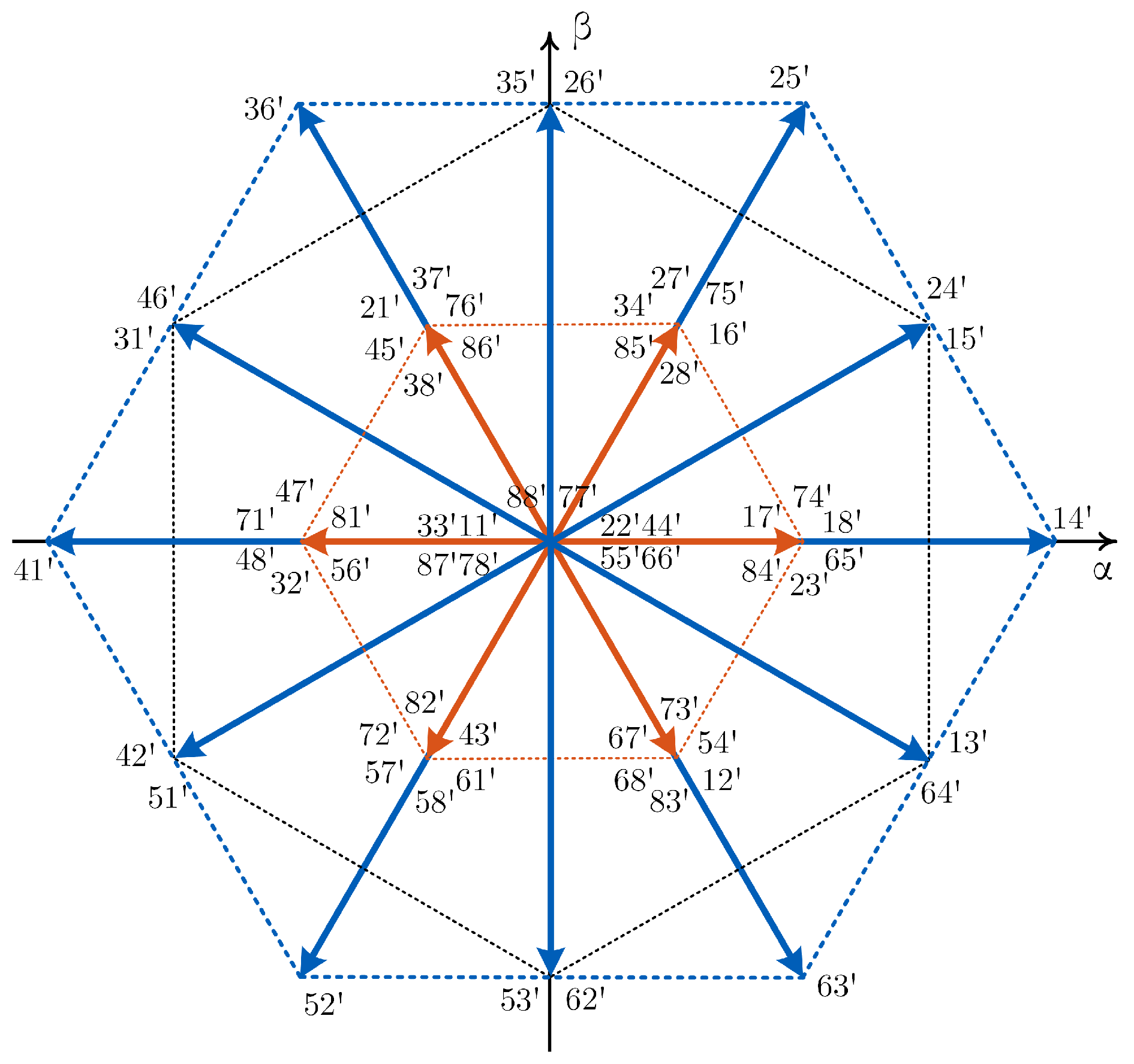
Since each inverter can assume eight different switching combinations, combining two inverters into the dual-inverter topology yields a total of 64 possible switching combinations. Yet, only 19 are unique while the rest are redundant, resulting in 18 different active vectors and a zero vector [
19]. The full set of fundamental voltage vectors of the dual-inverter topology, along with the corresponding states of both inverters, is depicted in
Figure 3. For example, the notation
signifies that vectors
and
are generated by INV1 and INV2, respectively, to produce the resulting voltage vector. Note that
Figure 3 is only valid when both inverters operate with the same DC-link voltage. Furthermore, this paper defines the modulation index
m as the ratio of the reference voltage vector magnitude to the maximum output voltage in the linear mode (when omitting inverter non-linearities), i.e.,
2.1. Modulation Techniques
When modulating the dual-inverter topology, one possible approach is to look at the system as a single multilevel inverter, leading to near-state-type pulse width modulation [
37]. Alternatively, the system can be viewed as two individual two-level inverters modulated separately by leveraging (
4) such that the desired voltage vector is applied to the load [
18]. The latter offers distinct advantages, namely, the option to utilize well-established carrier-based modulation techniques for two-level inverters, such as SVPWM or various bus-clamping strategies.
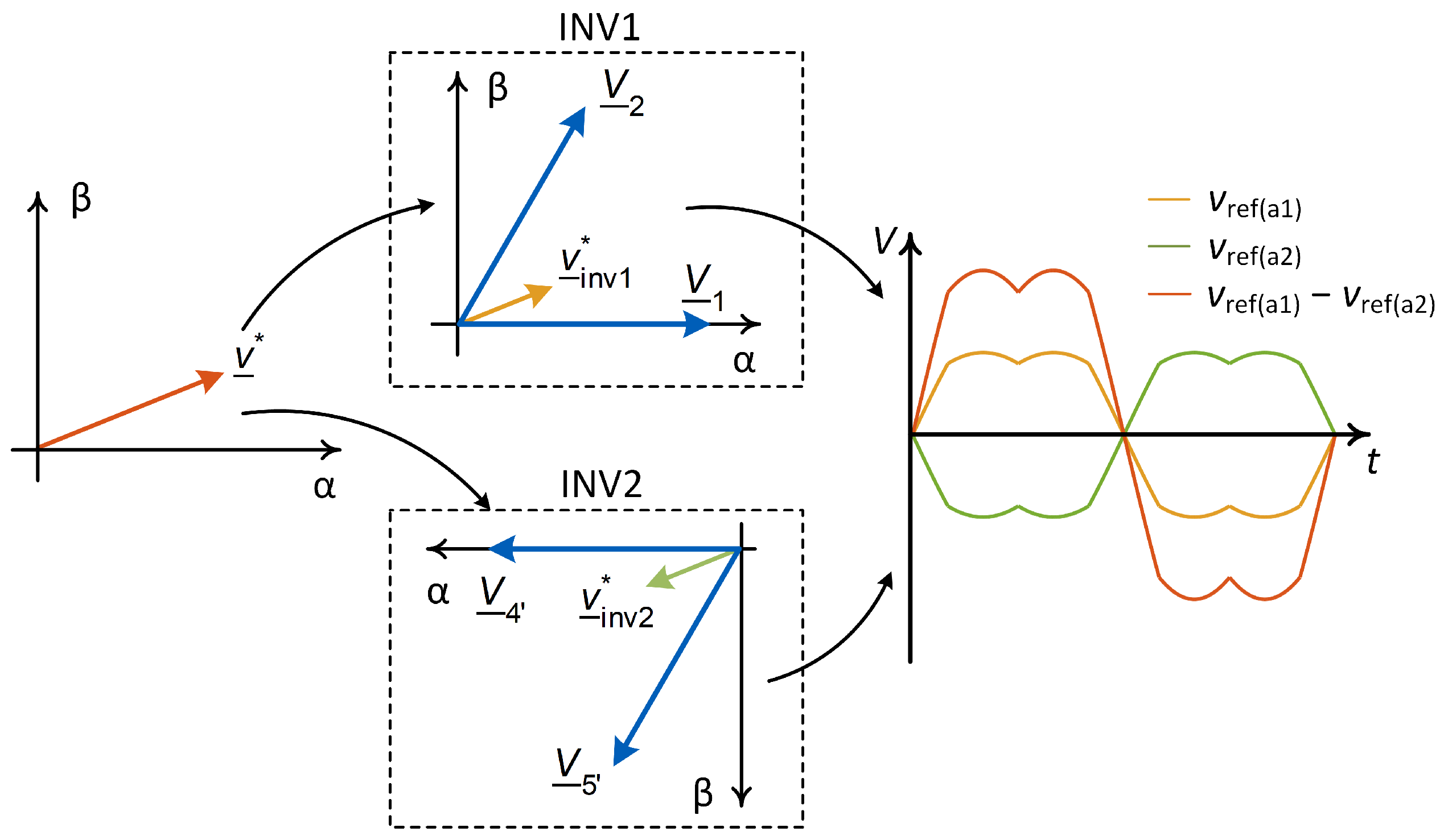
The most straightforward approach to combine the outputs of the two inverters to produce the desired voltage vector is to split the reference voltage into two equal components regardless of the value of
m, thus having each inverter generate half of the reference voltage throughout the whole linear region. In other words, suppose we have a reference voltage vector
coming from, e.g., a motor control algorithm. The modulator first splits the reference vector
into two sub-vectors
and
. Since equal DC-link voltages are assumed, the sub-vectors must have equal magnitudes to reach the maximum of the linear region. In mathematical terms,
To satisfy (
4), however, the reference sub-vector for INV2 must be phase-shifted by
. Therefore, regarding the phase of the sub-vectors, it holds that
To summarize, during every modulation period, both inverters synthesize a voltage vector of equal magnitude but with opposite phases. The whole process is illustrated in
Figure 4. Note that
Figure 4 also includes the reference modulation signals for the phase “a” when both inverters are modulated with SVPWM. Furthermore, the process described above can be used in conjunction with any carrier-based modulation technique.
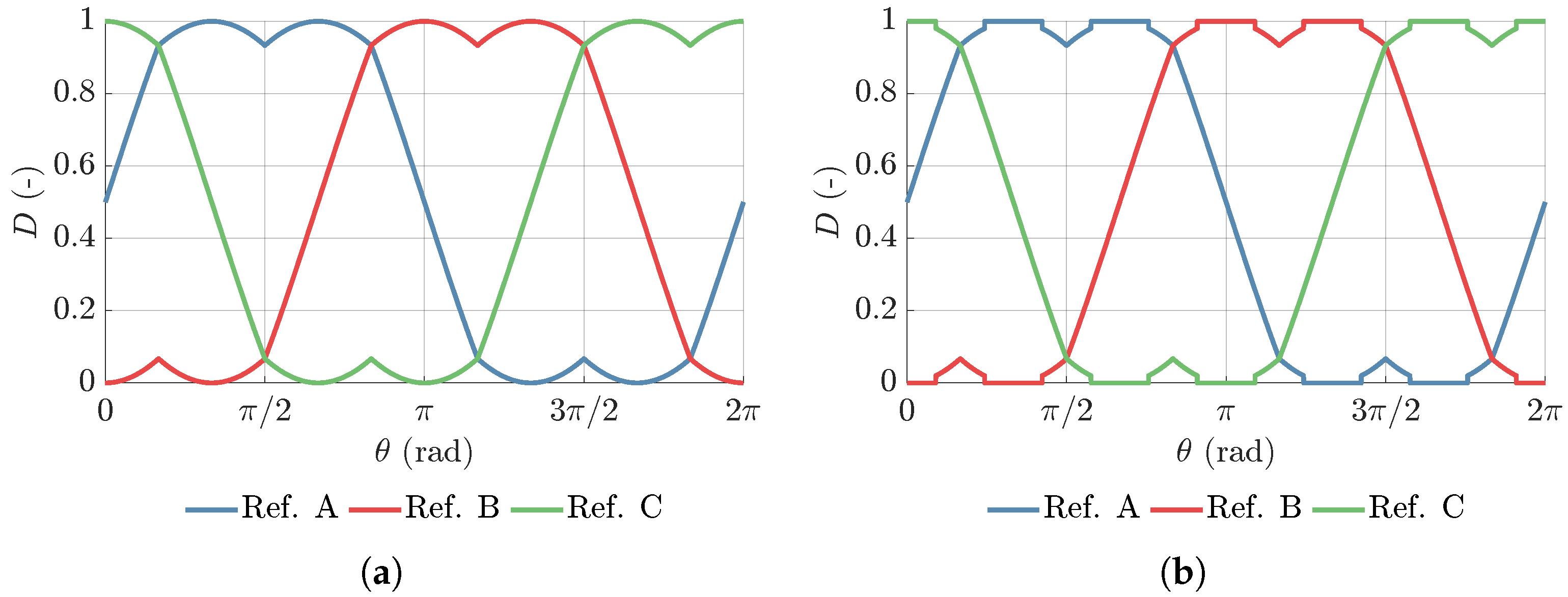
The overwhelming majority of literature utilizes the sector segmentation and subsequent switching time calculation approach to implement the SVPWM. While comprehensible, this approach presents an unnecessary computational burden on the microprocessor. Therefore, this paper uses the reference signal deformation [
34,
36] to implement the SVPWM. The reference three-phase voltages generated by the control algorithm are modified by a zero-sequence component as
The zero-sequence component
is calculated as
The resulting waveforms are compared with the triangular carrier signal to generate the switching actions for the inverter.
An alternative to the popular SVPWM is the bus-clamping strategies, also known as DPWMs. The main distinction is that for a set portion of the reference voltage period, either the upper or lower switch of a given inverter leg is permanently turned on and, consequently, only the complementary switch is modulated. Perhaps the most popular strategy is Depenbrock’s 60° discontinuous modulation—commonly referred to as DPWM1 [
34].
Analogously to SVPWM, the reference signal deformation can also be utilized for DPWM1. Although the process of finding the zero-sequence component is more tedious, it is still by far the fastest way to implement modulation. When implementing the DPWM1, first, the absolute value of the reference voltages is computed, then the phase with the highest magnitude is found [
36]. For the sake of explanation, let us assume that phase “a” has the highest magnitude; then the zero-sequence component is calculated as
The deformed and normalized reference voltages for SVPWM and DPWM1 are depicted in
Figure 5. The signals reach only positive values to reflect microprocessor implementation of the modulator, since in standard PWM modules, unsigned PWM timers are typically used.
3. Proposed Linear Region Subdivision
The method of splitting the reference voltage vector described above is straightforward and easy to implement; however, it is certainly not the most efficient one. This is mainly because, regardless of m, both inverters are always switching, even at times when the reference voltage is small enough that a single inverter would be capable of generating it. Consequently, both inverters operate with a small duty cycle, leading to greater distortion of the output voltage. Moreover, the switching losses are greater since twice the number of transistors are switching.
To improve upon the original method, we shall first examine
Figure 3. The entire voltage plane is dominated by three hexagons, of which the inner red one and outer blue one are of particular interest. The area bounded by the red hexagon represents all possible states reachable by just a single inverter, with the other one having either all upper or lower switches closed, thus effectively creating a neutral point for the motor winding. In contrast, the blue hexagon bounds the states that can only be reached by cooperation of both inverters. In other words, if the reference voltage vector stays within the red hexagon, only a single inverter is modulated, while a zero vector is permanently applied to the other one. Meanwhile, whenever the reference voltage vector moves beyond the red hexagon, both inverters must be modulated to generate the desired voltage vector.
Based on the previous analysis, the voltage plane can be divided into three distinct regions (see
Figure 6), where, for the sake of clarity, only the first sector is shown. The “base region” is bounded by the inscribed circle of the red hexagon, representing the linear region of a single inverter. Beyond the “base region” lies the “transition region”, upper-bounded by the circumscribed circle of the red hexagon. It represents the area where the reference voltage vector trajectory partially exceeds the red hexagon. Finally, when the reference vector trajectory fully exceeds the red hexagon, the “extended region” is reached. Since equal DC-link voltages are assumed, it does not matter which inverter is set to operate in the “base region”. However, for further explanations, it is helpful to select, e.g., INV1 as the main inverter while leaving INV2 as the secondary inverter. The boundaries between the individual regions can also be given in terms of the modulation index
m, defined in (
5) as follows:
Base region: The main inverter is switching while a zero vector is permanently applied to the secondary inverter, resulting in an operation identical to a single two-level inverter.
Transition region: The main inverter operates permanently on the boundary of its linear region, while in areas where the reference vector trajectory exceeds the red hexagon, the secondary inverter is also modulated to generate the reference voltage.
Extended region: Both inverters are modulated at all times.
The bounds of the transition region in terms of
m can be derived as follows: since equal DC bus voltages are assumed, each inverter can supply up to half of the total voltage since its DC-link voltage is equal to
. Therefore, when only a single inverter is switching while the other creates a neutral point, the operation is restricted to the smaller orange hexagon (see
Figure 6). Consequently, the threshold of its linear region is reached when the reference voltage vector
magnitude is equal to
As a result, the threshold of the linear region when only a single inverter is switching corresponds to the modulation index of
as per (
5). Increasing the magnitude of the reference voltage vector further causes its trajectory to partly exceed the boundary of the inner hexagon. Consequently, the other inverter starts switching to maintain the linear modulation mode. In such an operation, the transition region continues until the circumscribed circle of the inner hexagon is reached. This happens when
which corresponds to
.
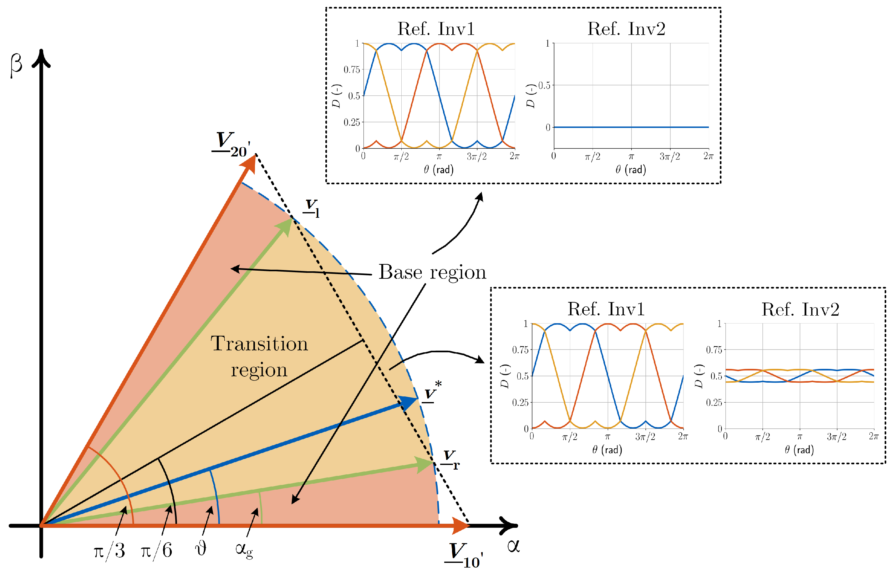
Detailed Operation in Transition Region
While the operation in both the “base” and “extended regions” is relatively straightforward, the “transition region” requires closer attention.
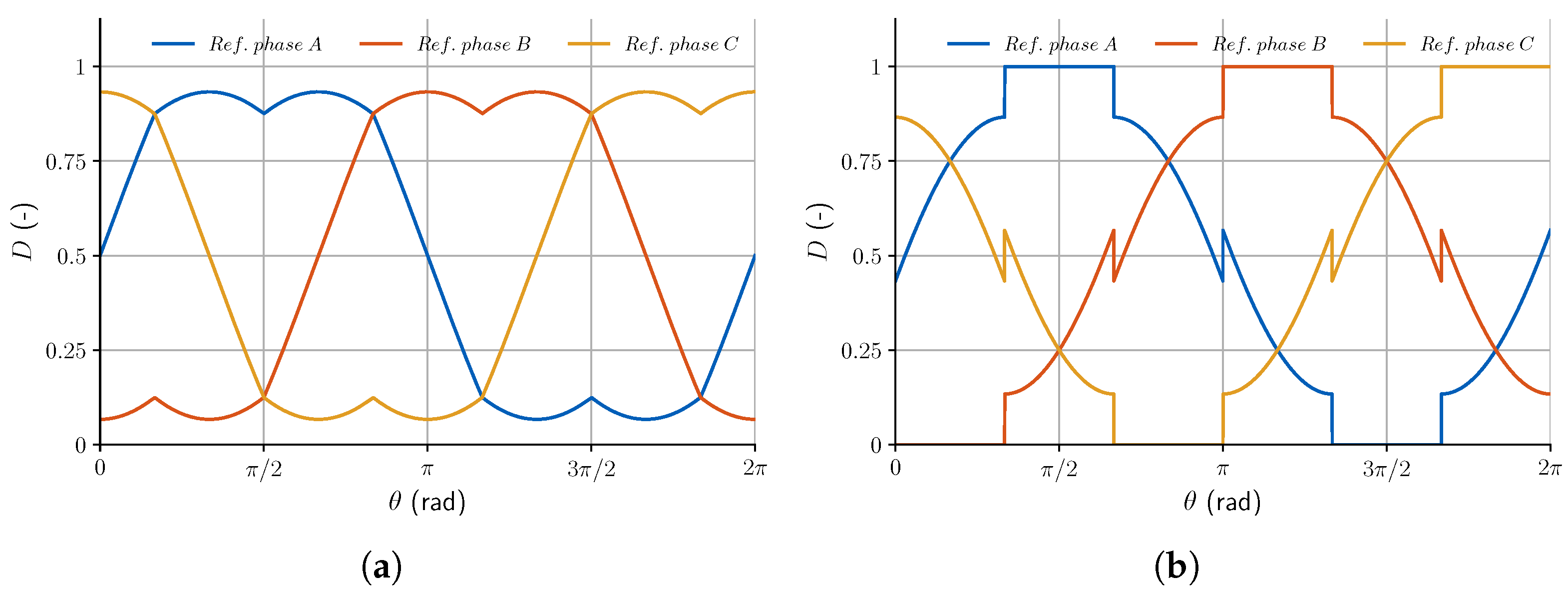
Figure 7 illustrates the working principle of the modulator within the “transition region” for the first sector.
For further clarification,
Figure 7 also includes the corresponding normalized modulation signals when SVPWM is used; the identical principle is applied when a different modulation method is used. Note that a value of “1” corresponds to the upper switch being closed for the entire modulation period, while “0” represents the lower one being closed during the whole modulation period.
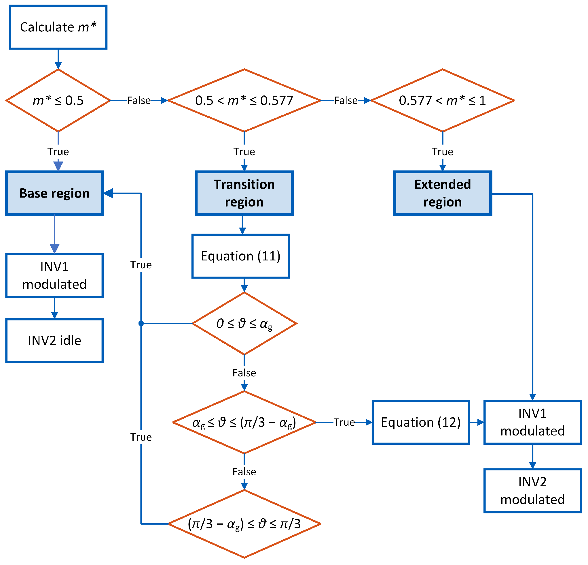
The subdivision of the whole linear region of the dual-inverter topology is depicted in the form of a flowchart in
Figure 8. For the sake of clarity, the decision tree for the “transition region” is shown only for the first sector, since the operation in the other sectors is analogous.
4. Results
4.1. Simulation Setup
The simulation encompassed multiple operational modes of the DI and various operation states of the squirrel cage IM acting as a load. The tested operational modes of the DI are outlined as follows:
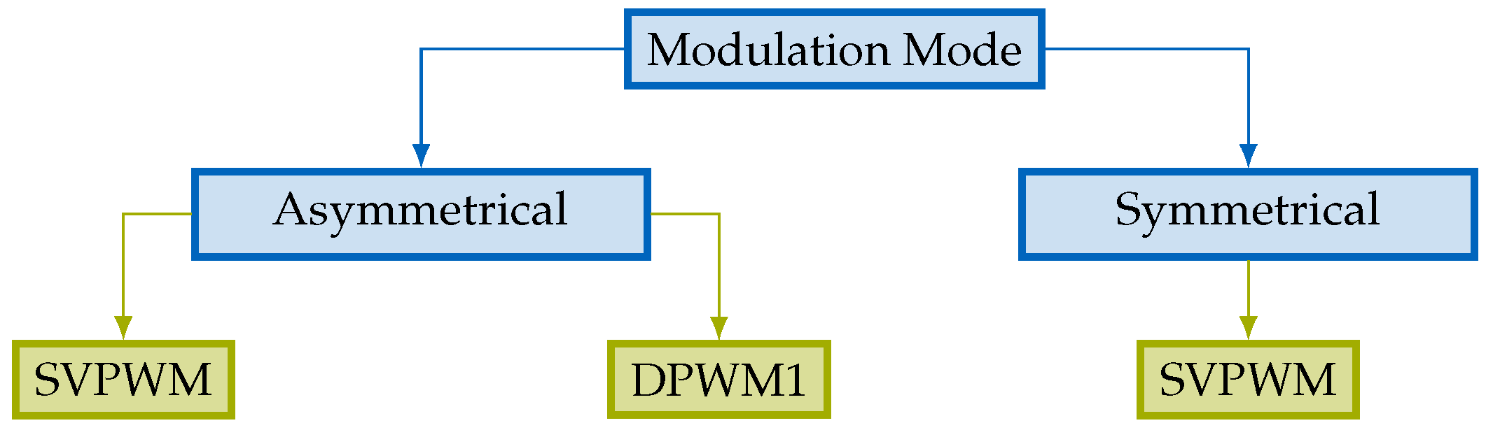
Modulation Mode Symmetrical: The output voltage is synthesized from both inverters working together, and the reference voltage is equally distributed.
Modulation Mode Asymmetrical: For , only one inverter is active while the second inverter creates a neutral point. For , the reference voltage vector is distributed asymmetrically between both inverters. The main inverter operates on the boundary of its linear region, and the second inverter synthesizes the remaining voltage.
Modulation strategies SVPWM, DPWM 1: The names correspond to the strategies presented in
Section 2.1.
Relations between the simulated variants are depicted in
Figure 9. The implementation of the dead time (selected as 100 ns), along with the limitation of the minimum and maximum width of the switching pulse (selected as 2% and 98%, respectively), were carried out to ensure model realism.
The simulations were executed in the MATLAB R2023b Simulink environment, leveraging the Simscape Electrical library. As a solver, the ODE4 (Runge–Kutta) solver with fixed step (as shown in
Table 1) was employed.
Given the extensive nature of the model and the necessity to obtain data across multiple operational points, the simulations were conducted in parallel, employing the parsim function from Parallel Computing Toolbox. The parallel simulation parameters were configured before the parallel simulation started using a MATLAB script and parsim properties.
The squirrel cage IM served as the load for the DI, and the predefined Simscape Electrical model was used for the simulation. The motor was modeled using the Simscape
Induction Machine Squirrel Cage and it was parameterized using real-world measurements obtained from an existing laboratory motor, as shown in
Table 2. This approach ensured that the model closely mirrored the performance characteristics of the physical motor. The Simscape
Ideal Torque Source block was used as a mechanical load for the IM. Common parameters for all conducted simulation variants are shown in
Table 1.
In MATLAB/Simulink, the switching components were modeled using the Simscape Electrical Ideal MOSFET block with an enabled thermal port. The switching components were automatically and precisely parameterized using the Block Parameterization Manager included in Simscape. This feature contains a detailed parametrization of various MOSFETs directly from the corresponding manufacturer. Based on the DC supply voltage level, load current, and carrier wave frequency, the SiC transistors STMicroelectronics SCTWA35N65G2V were selected for the simulation purposes.
When the thermal port is enabled, the MOSFET model allows for switching loss parametrization via a look-up table. Subsequently, at every switching instance, the MOSFET model calculates the switching losses based on the transistor voltage and current at the time of switching. This eliminates the necessity to simulate the switching transients, significantly increasing the minimum required solver step size and making the model much more feasible to simulate.
Upon the successful completion of the simulation, the selected recorded data were saved to a corresponding MAT file for subsequent processing. The reported efficiency and losses, dependent on the modulation index, were obtained from the motor steady-state at a specific working condition (averaging the data in a small time window near the end of the simulation). Therefore, only a portion of the data was saved to reduce the size of the MAT files. The figures illustrating time-dependent data series were derived from the entirety of the simulation, ensuring comprehensive insights into the dynamic behavior of the DI and IM.
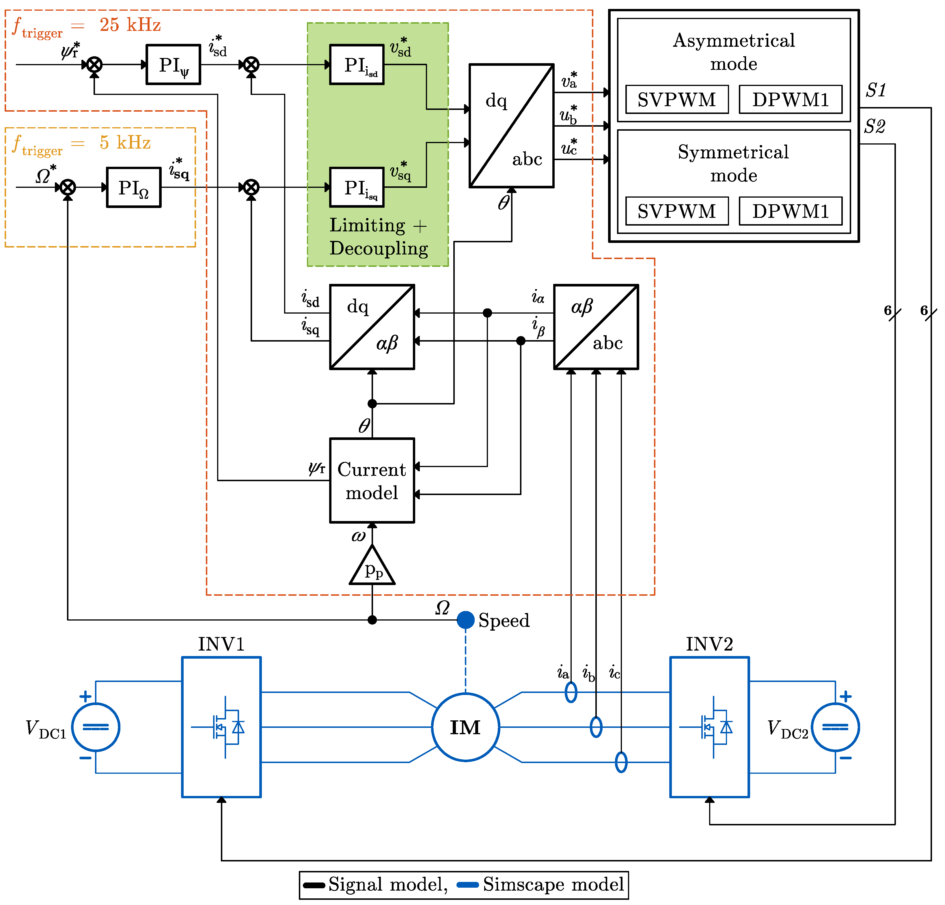
The block diagram of the simulation setup is depicted in
Figure 10. The figure illustrates the use of FOC in the motor drive system. FOC utilizes the conventional and simple current-speed motor model. Reference values are computed using Simulink
Triggered Subsystems controlled by square wave trigger signals. This approach models the use of a microcontroller, calculating new reference values in a stable-frequency manner, in this case lower than the frequency of the carrier wave signal.
Conventional discrete-time PI controllers were utilized in the FOC model, whose gains were tuned using a trial and error approach. A simplified model of an induction machine with FOC was utilized for this purpose. As a result, the simulation speed was considerably improved, streamlining the process of tuning the controllers. Subsequently, the controllers were incorporated into the expanded Simulink model, where both the inverters and IM are modeled using Simscape blocks, as depicted in
Figure 10, with final fine-tuning performed. The gains of the respective controllers are summarized in
Table 3.
4.2. Simulation Results
For a thorough comparison of the presented modulation strategies, fifteen operating points were systematically examined. The consistent conceptual framework across all simulations involved nominal excitation of the machine, followed by issuing a specific speed command at s and loading the machine with at s. Maintaining a constant load torque at all speeds ensured a uniform current at each operating point, thereby keeping conduction losses constant. This approach facilitates a precise quantification of the reduction in switching losses thanks to the proposed strategy.
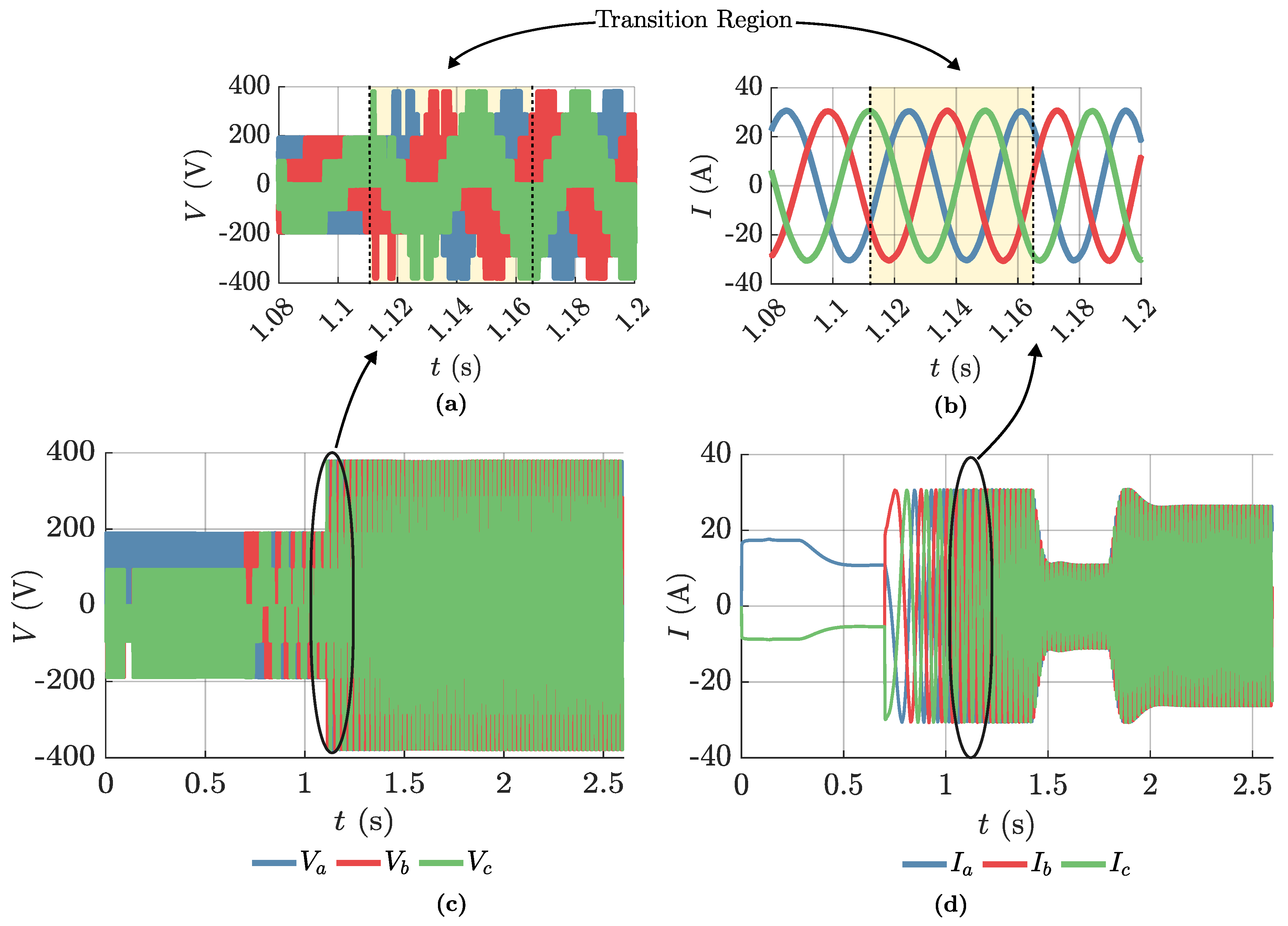
The operational characteristics of the proposed asymmetrical modulation scheme concerning motor phase voltages and currents are illustrated in
Figure 11, where SVPWM was employed to modulate both inverters.
Figure 11c reveals motor phase voltages throughout the simulation, highlighting the key feature of the proposed scheme: only one inverter is modulated when sufficient to supply the required voltage.
Figure 11a details operation in the transition region when a single inverter is insufficient, leading to the activation of the second inverter. Lastly,
Figure 11b verifies the smooth transition from single- to dual-inverter operation in terms of motor phase currents. The results confirm the feasibility of the proposed strategy.
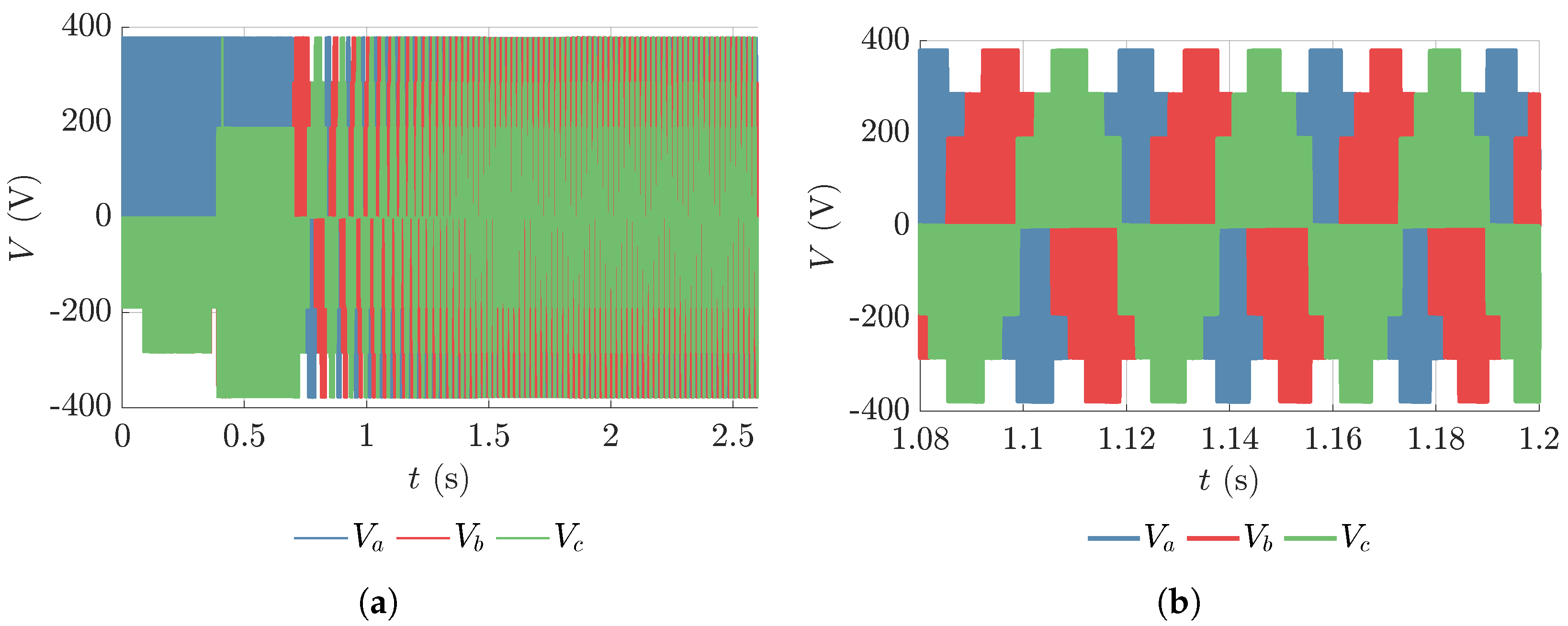
To highlight operational differences,
Figure 12 depicts motor phase voltages using symmetrical SVPWM.
Figure 12a shows the phase voltages throughout the simulation, while
Figure 12b focuses on selected periods. Symmetrical SVPWM applies full dual-inverter DC-bus voltage regardless of
m, resulting in unchanged voltage waveforms.
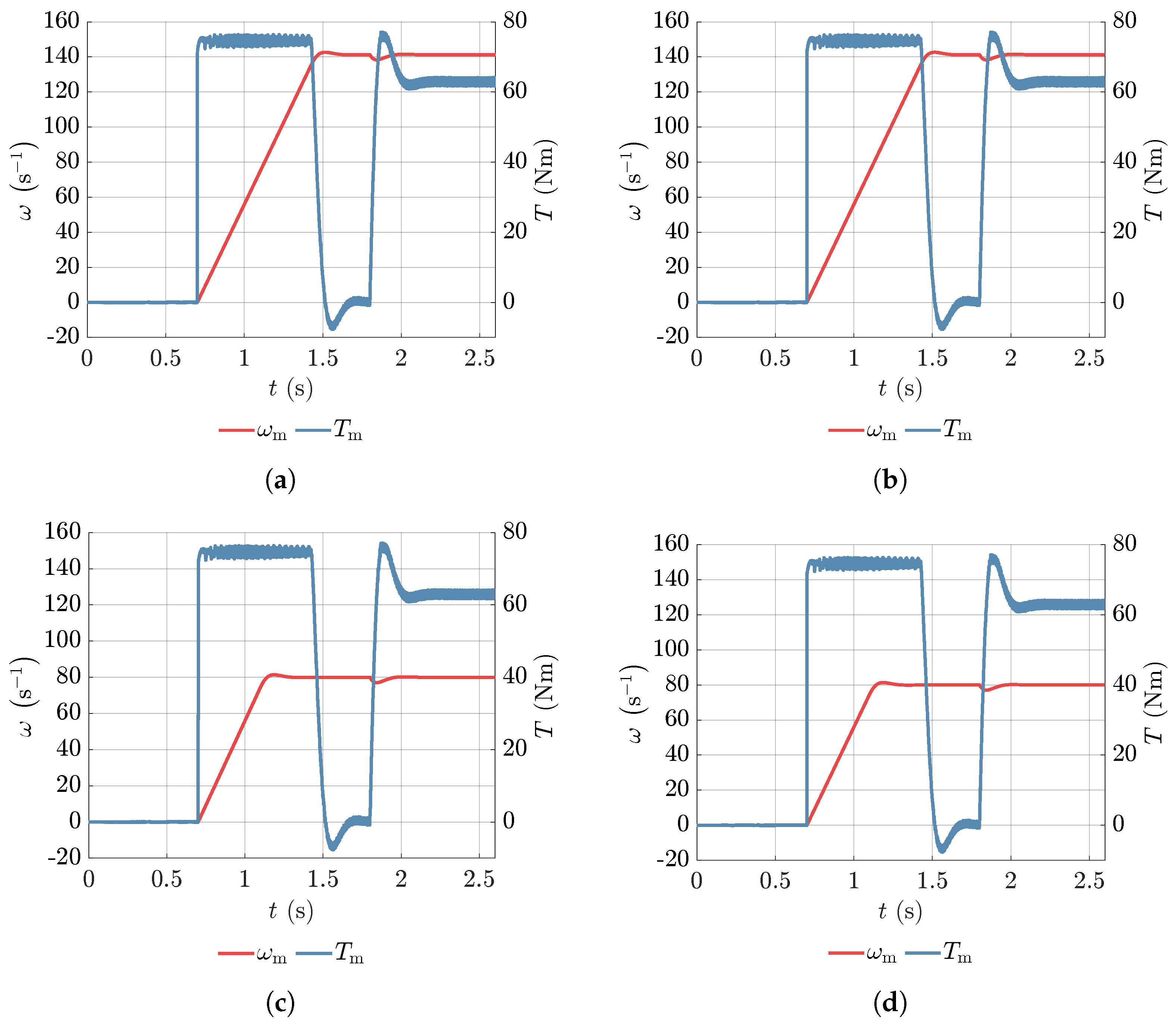
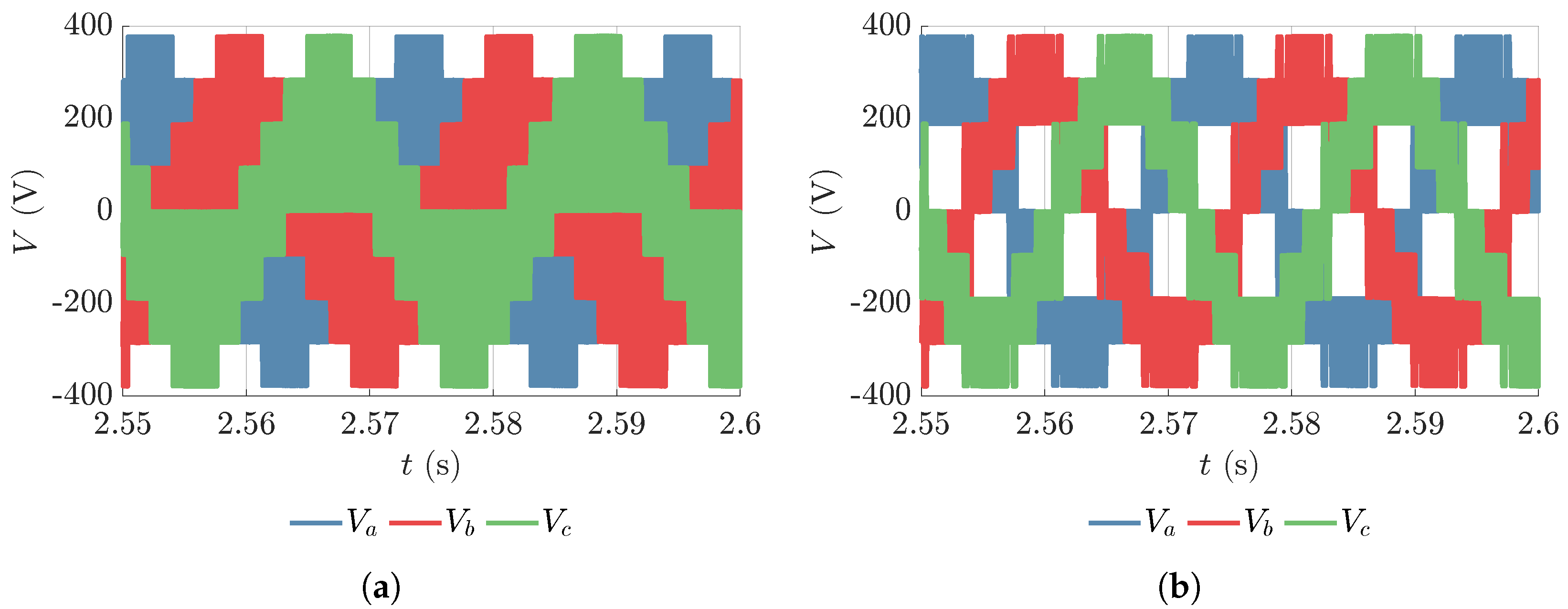
Figure 13 shows the motor speed and torque during the acceleration towards two different target speeds for both asymmetrical SVPWM and DPWM1. The left column corresponds to asymmetrical SVPWM, and the right column represents asymmetrical DPWM1. The drive exhibits smooth and stable performance in all cases without any unwanted transients, validating the proposed modulation approach.
Noticeably, when SVPWM is used, the motor exhibits a slightly higher torque ripple compared to DPWM1, which is consistent with worse motor phase current distortion (THD:
,
). This is attributed to the instantaneous phase voltage dropping to zero in SVPWM, causing greater voltage differences between consecutive switching instances and, consequently, a higher current ripple. In DPWM1, the voltage change occurs only between consecutive voltage levels, reducing current and torque distortion. The respective voltage waveforms are depicted in
Figure 14.
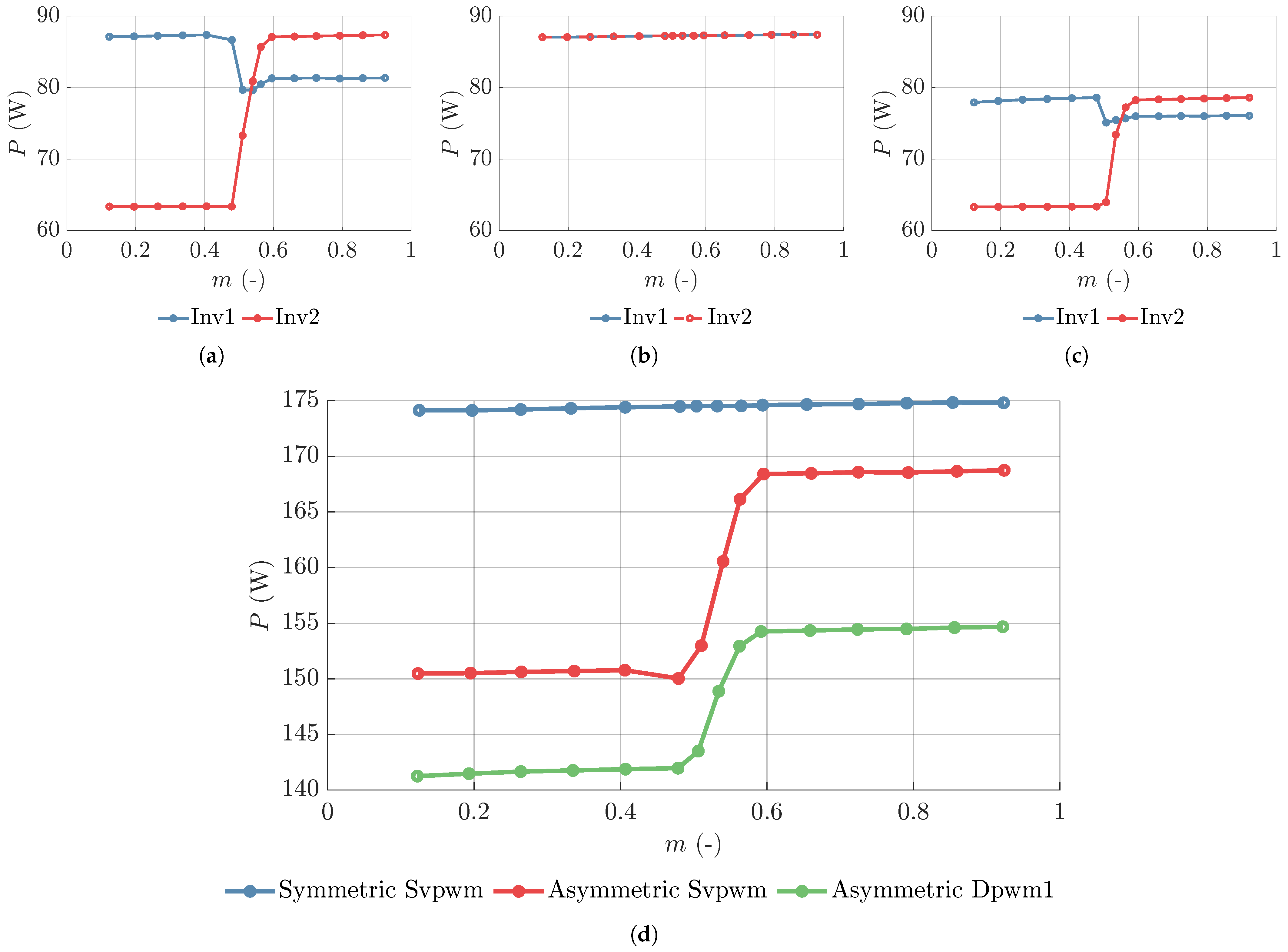
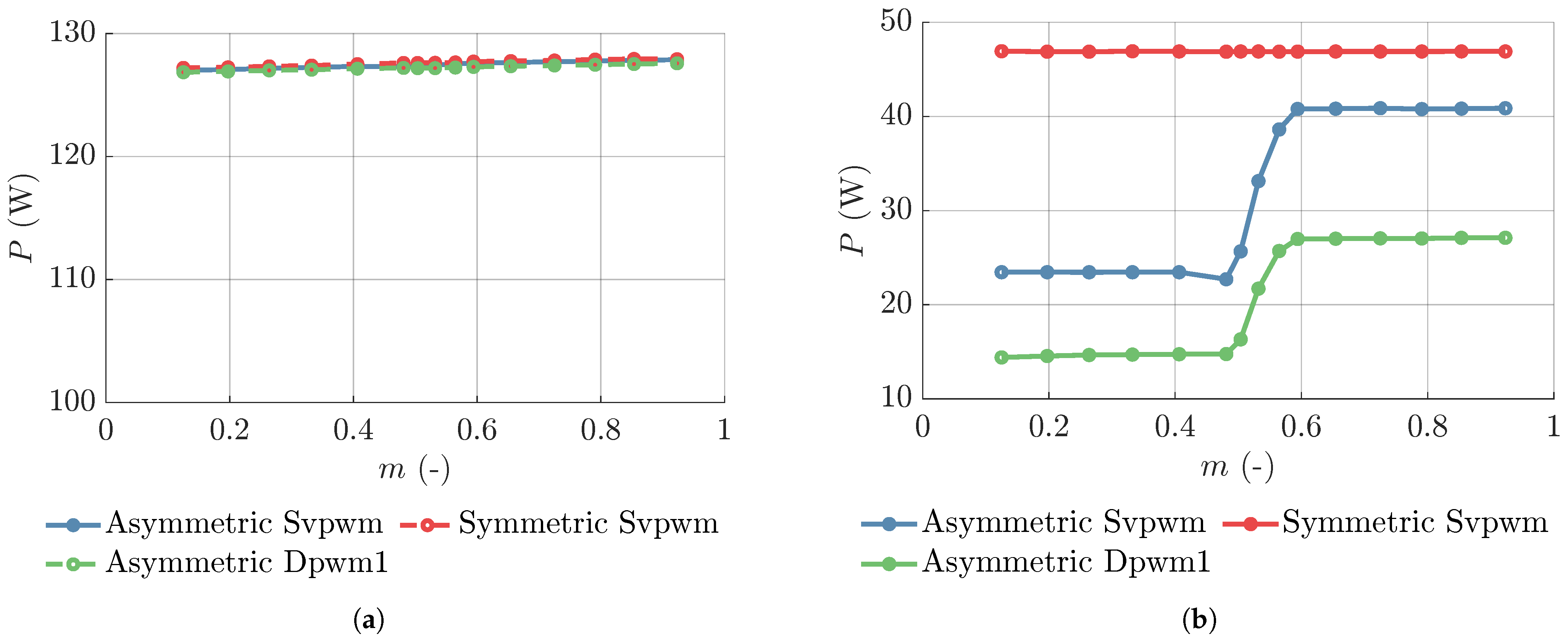
The primary motivation behind the proposed asymmetrical modulation scheme was to reduce switching losses. The detailed steady-state loss analysis is presented in
Figure 15. In
Figure 15a, the total losses of each inverter under asymmetrical SVPWM are shown. The losses are plotted as a function of
m. When
, only INV1 is modulated, and INV2 is idle with all low-side switches turned on to create a neutral point. Consequently, INV2 only incurs conduction losses, unaffected by the value of
m, as the current through the converter remains constant. Conversely, INV1 suffers from both conduction and switching losses.
When m surpasses the threshold of , INV1 is no longer sufficient to supply the load with the required voltage. Therefore, INV2 becomes active, i.e., starts to be modulated. Consequently, the total losses of INV2 rapidly increase as switching losses become prevalent. Simultaneously, the losses of INV1 decrease due to the minimum pulse width limitation. The minimum pulse width is set to . Consequently, when the pulse width drops below the specified threshold, the zero vector is omitted, and instead, the corresponding phase is clamped to either the positive or negative DC-bus rail. As a result, the SVPWM transforms into a pseudo-bus-clamping strategy.
Clamping each phase to either DC-bus rail reduces the number of switching instances, causing a reduction in switching losses. Such pulse width limitation introduces slight non-linearity to the modulation; nevertheless, as
Figure 11 and
Figure 13 confirm, the current controllers compensate for it completely. For clarity, the original and deformed reference waveforms are depicted in
Figure 16.
In
Figure 15b, the cumulative losses of both inverters under conventional symmetrical SVPWM are depicted. As anticipated, both inverters incur identical losses across the entire linear region. A comparison with
Figure 15a underscores the potential for reducing losses when employing the proposed asymmetrical modulation scheme.
This potential for loss reduction becomes even more pronounced when DPWM1 is employed instead of SVPWM in the asymmetrical scheme (refer to
Figure 15c). The well-established properties of DPWM1 in reducing switching losses, as observed in conventional two-level inverters, extend to this context, resulting in a further decline in converter losses. Analogous to SVPWM, the minimum pulse width limitation contributes to an additional reduction in switching losses.
Figure 15d shows the aggregate losses of the dual-inverter system, calculated as the sum of losses from individual inverters. Evidently, there is a significant reduction in losses when adopting the proposed asymmetrical SVPWM modulation scheme, as opposed to the conventional practice of modulating both inverters simultaneously. Furthermore, the asymmetrical modulation scheme, owing to the minimum pulse width limitation, surpasses the symmetrical approach even when both inverters are modulated. Additionally, substituting SVPWM with DPWM1 leads to a further decline in converter losses.
Furthermore,
Figure 17 depicts the separation of the total steady-state losses into conduction and switching losses. Conduction losses remain constant over the entire linear region since six transistors are conducting at any given point, irrespective of the modulation strategy. The switching losses, however, vary significantly, highlighting the potential improvement in efficiency by selecting an appropriate modulation strategy.
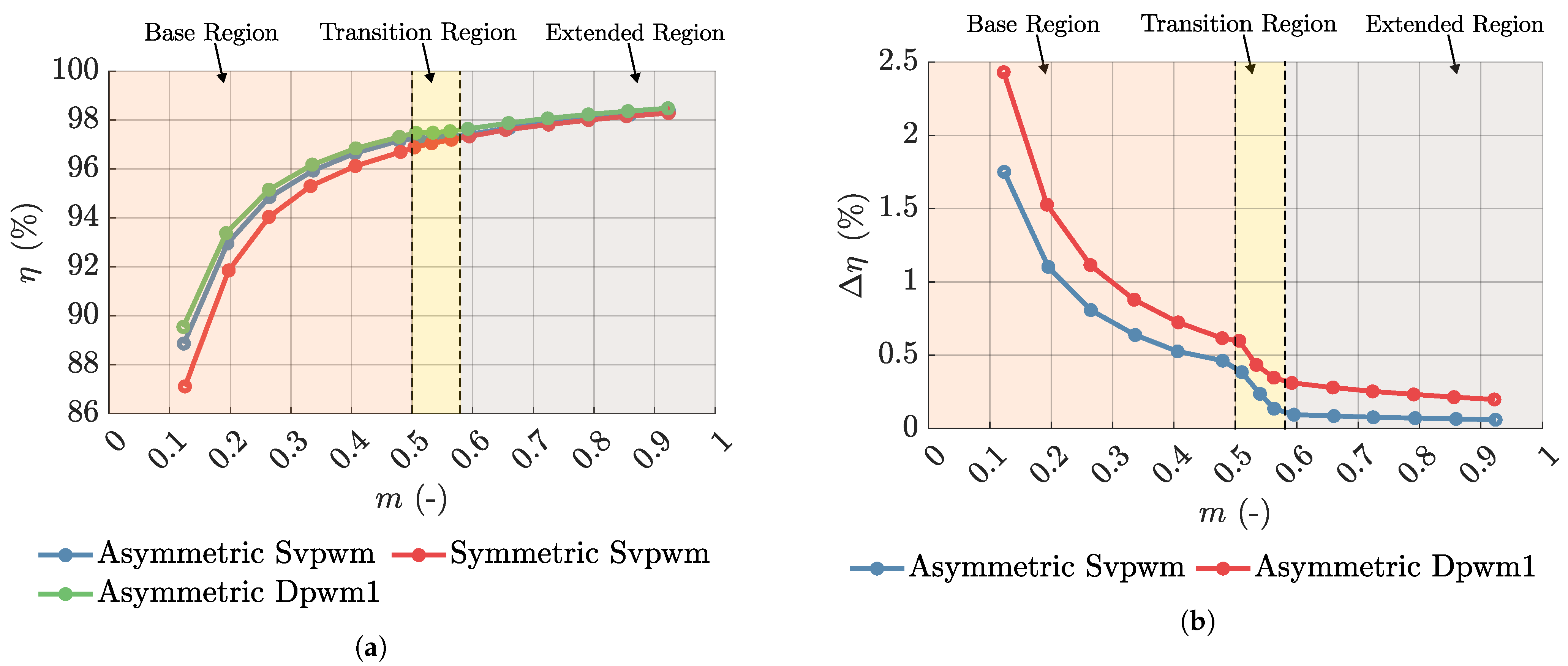
Finally, the effectiveness of the proposed asymmetrical modulation technique can be quantified in terms of the drive efficiency improvement.
Figure 18a illustrates the total drive system efficiency as a function of
m for various modulation strategies. Clearly, symmetrical SVPWM produces the least favorable outcome, particularly in the base region, while asymmetrical DPWM1 maintains the highest efficiency across the entire operating range. Asymmetrical SVPWM exhibits a significant improvement over symmetrical SVPWM but is surpassed by the asymmetrical DPWM1. The efficiency enhancement resulting from the asymmetrical strategies compared to symmetrical SVPWM is presented in
Figure 18b. Clearly, employing asymmetrical DPWM1 enhances drive efficiency by up to 2%, while not going below a difference of 0.5%, even in the “base region”. Asymmetrical SVPWM offers a slightly lower efficiency improvement compared to the symmetrical variant, though still substantial.
To highlight the key differences between the studied modulation techniques,
Table 4 quantifies the performance of each modulation method in terms of total losses and the corresponding efficiency improvement in the base region as well as the transition region.
5. Discussion
Electric drives operating as traction drives must maintain nominal torque until voltage limitations necessitate the onset of field weakening. In the context of AC drives employing field-oriented control (FOC), sustaining constant-torque operation equates to maintaining a constant AC current drawn from the converter. When the machine is powered by a dual inverter, the synthesis of the reference voltage vector from the FOC algorithm provides a high degree of freedom, allowing for flexibility in the modulation strategy employed.
The asymmetrical modulation mode, wherein only one inverter operates while the other establishes a neutral point, was the first option explored and is viable up to approximately half of the nominal speed. Beyond this point, the first inverter remains at its maximum in a linear modulation mode, with the second inverter gradually contributing to the reference voltage vector up to the nominal speed. In contrast, the symmetrical modulation mode evenly distributes the reference voltage vector between the two inverters in a 1:1 ratio.
The asymmetrical modulation mode demonstrated a significant reduction in switching losses below and, surprisingly, above half of the nominal speed compared to the symmetrical mode. Additionally, Depenbrock’s discontinuous modulation (DPWM1) proved superior in minimizing inverter losses when compared to Space Vector PWM (SVPWM), attributed to its bus-clamping nature, which improves the quality of voltage, current, and torque waveforms. The harmonic behavior of SVPWM and DPWM strategies in the dual-inverter topology diverges from that in the classic single inverter, offering an opportunity for further research.
The efficiency gains achievable by selecting a modulation strategy and voltage vector distribution (i.e., solely by software modifications) for the dual-inverter topology are evident below half of the nominal speed. This efficiency increase, in the range of units of percent, is relatively substantial in the context of modern power converters, making it an interesting option for battery-powered electric vehicles or aircraft. While the strategy has been validated on a conventional induction motor, it is not bound to a specific type of machine and can also be applied to permanent magnet or reluctance machines.


