
The Impact of a Number of Samples on Unsupervised Feature Extraction, Based on Deep Learning for Detection Defects in Printed Circuit Boards


Abstract
:1. Introduction
2. Review
2.1. Traditional Computer Vision-Based Techniques
2.2. Machine Learning-Based Techniques
3. Problem Posing
4. Materials and Methods
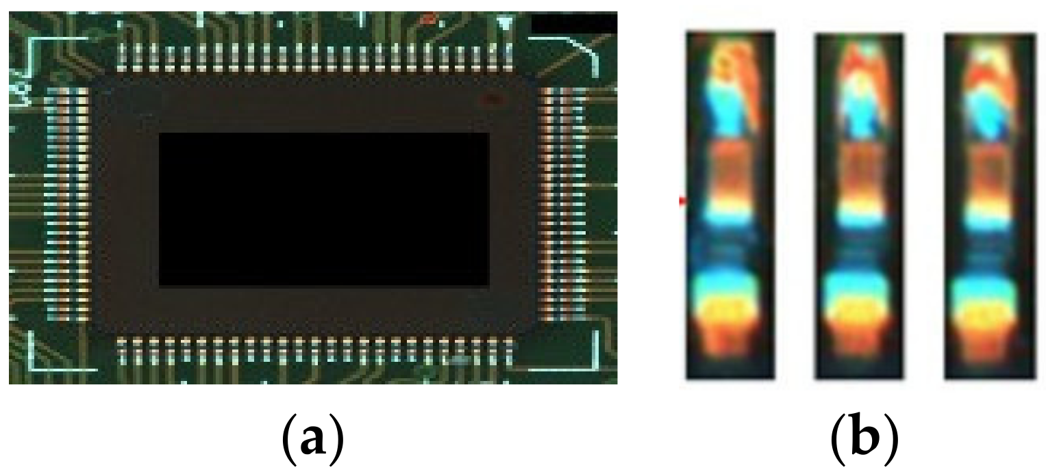
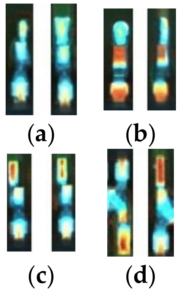
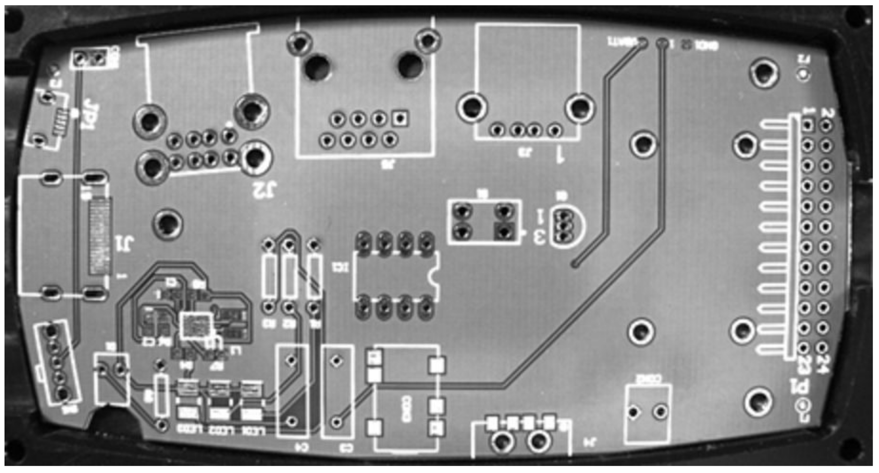
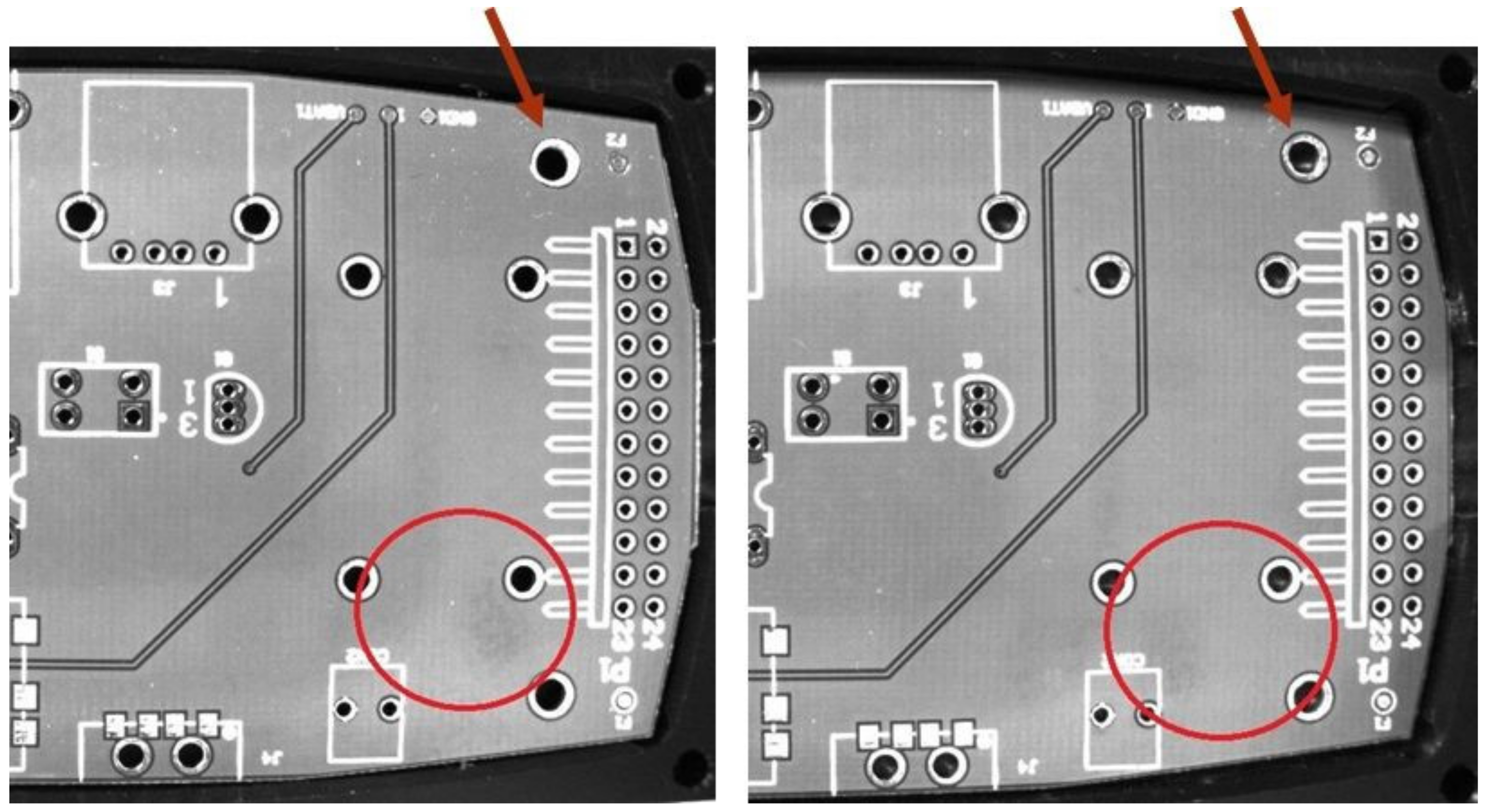
4.1. Dataset Description
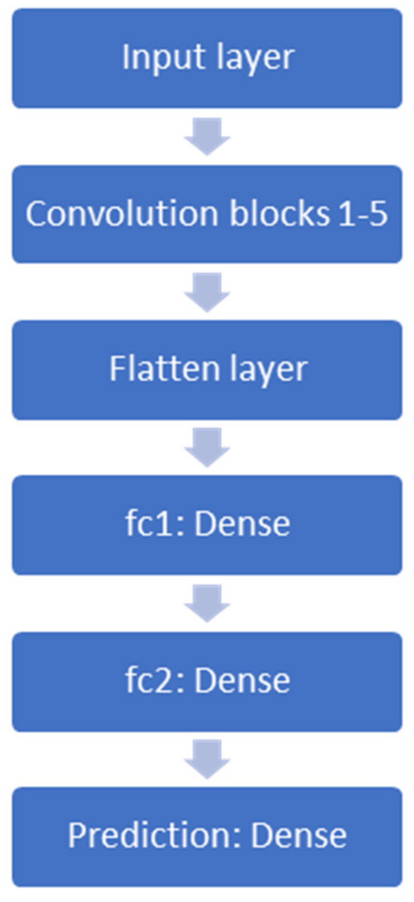
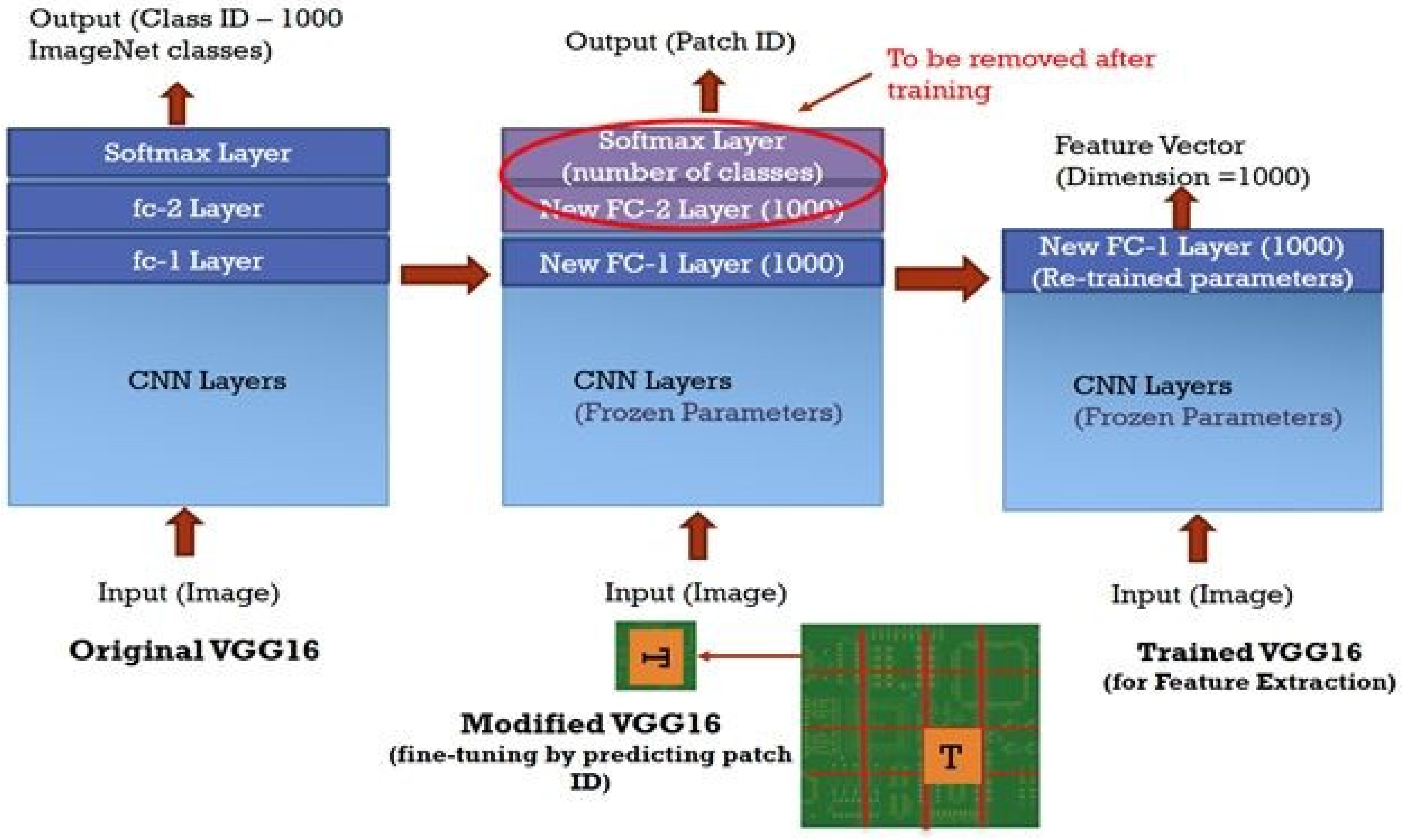
4.2. Model Architecture ane Experiment Description
- To choose the size of the patch comparable to the size of individual elements, as too small patch size will lead to extra sensitivity to normal minor changes, and too large patch size will result in a lack of discriminative power to detect and localize the defect. The patch size will affect the number of classes K, in which our PCB will be divided.
- To feed the patches randomly rotated by 0, 90, 180, and 270 degrees to the described configuration of the network.
- where, ,
- and
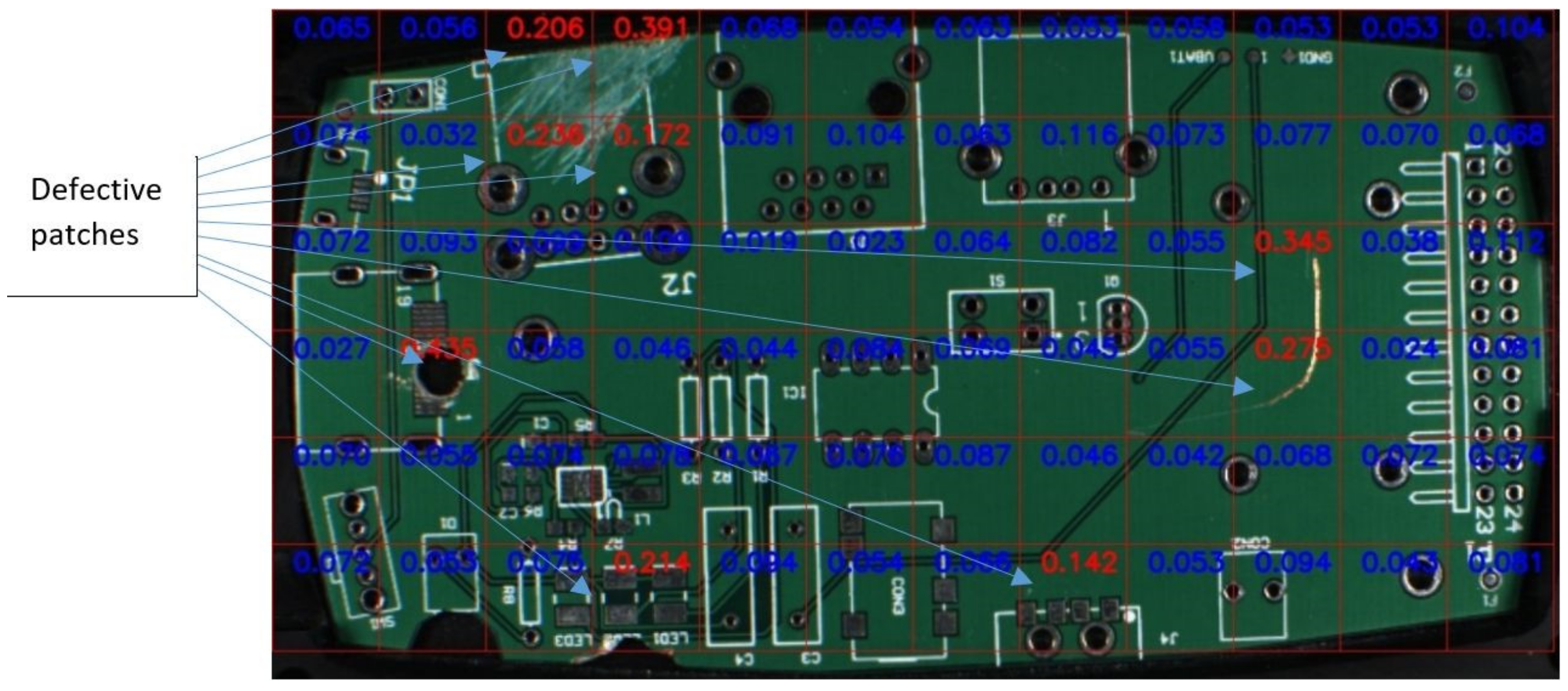
- and TP, TN, FP, and FN are the numbers of true positive, true negative, false positive, and false negative, respectively. The F1 score is the harmonic mean of precision and recall (sensitivity). The Matthews correlation coefficient (MCC) [37] is a measure of the quality of binary (two-class) classifications. It considers true and false positives and negatives and is generally regarded as a balanced measure that can be used, even if the classes are of very different sizes. The MCC is a correlation coefficient between the observed and predicted binary classifications. It returns a value between −1 and +1. A coefficient of +1 represents a perfect prediction, 0 represents no better than random prediction, and −1 indicates total disagreement between prediction and observation. The MCC score is high only if the classifier is doing well on both the negative and positive samples.
5. Findings
6. Discussion and Implications
Analysis of Results and Future Work
- How to detect whether the sample is representative or not adding much to training;
- How to form a representative set of samples;
- Whether the traditional computer vision techniques could be combined with machine learning to improve the accuracy.
7. Conclusions
Author Contributions
Funding
Data Availability Statement
Conflicts of Interest
References
- Moganti, M.; Ercal, F.; Dagli, C.H.; Tsunekawa, S. Automatic PCB Inspection Algorithms: A Survey. Comput. Vis. Image Underst. 1996, 63, 287–313. [Google Scholar] [CrossRef] [Green Version]
- Anitha, D.B.; Rao, M. A survey on defect detection in bare PCB and assembled PCB using image processing techniques. In Proceedings of the 2017 International Conference on Wireless Communications, Signal Processing and Networking (WiSPNET), Chennai, India, 22–24 March 2017; pp. 39–43. [Google Scholar]
- Taha, E.M.; Emary, E.; Moustafa, K. Automatic optical inspection for PCB manufacturing: A survey. Int. J. Sci. Eng. Res. 2014, 5, 1095–1102. [Google Scholar]
- Drury, C.G.; Sinclair, M.A. Human and Machine Performance in an Inspection Task. Hum. Factors J. Hum. Factors Ergon. Soc. 1983, 25, 391–399. [Google Scholar] [CrossRef]
- Huang, S.-H.; Pan, Y.-C. Automated visual inspection in the semiconductor industry: A survey. Comput. Ind. 2015, 66, 1–10. [Google Scholar] [CrossRef]
- Zhang, C.; Shi, W.; Li, X.; Zhang, H.; Liu, H. Improved bare PCB defect detection approach based on deep feature learning. J. Eng. 2018, 2018, 1415–1420. [Google Scholar] [CrossRef]
- Wu, W.-Y.; Wang, M.-J.J.; Liu, C.-M. Automated inspection of printed circuit boards through machine vision. Comput. Ind. 1996, 28, 103–111. [Google Scholar] [CrossRef]
- Eun, H.Y.; Seung, H.P.; Cheong-Sool, P.; Jun-Geol, B. Feature-learning-based printed circuit board inspection via speeded-up robust features and random forest. Appl. Sci. 2018, 8, 932. [Google Scholar]
- Kim, H.W.; Yoo, S.I. Defect detection using feature point matching for non-repetitive patterned images. Pattern Anal. Appl. 2012, 17, 415–429. [Google Scholar] [CrossRef]
- Dahlgaard-Park, S.M. Define, Measure, Analyze, Improve, and Control (DMAIC) Process. In The SAGE Encyclopedia of Quality and the Service Economy; SAGE Publications, Inc.: New York, NY, USA, 2015; Volume 1, pp. 141–143. [Google Scholar]
- Tikhe, C. Metal surface inspection for defect detection and classification using Gabor Filter. Int. J. Innov. Res. Sci. Eng. Technol. 2014, 3, 13702. [Google Scholar]
- Timm, F.; Barth, E. Non-parametric texture defect detection using Weibull features. In Proceedings of the IS&T/SPIE Electronic Imaging, San Francisco, CA, USA, 23–27 January 2011. [Google Scholar]
- Wang, Z. Image quality assessment: From error visibility to structural similarity. IEEE Trans. Image Process. 2004, 13, 600–612. [Google Scholar] [CrossRef] [Green Version]
- Carro, R.C.; Larios, J.-M.A.; Huerta, E.B.; Caporal, R.M.; Cruz, F.R. Face Recognition Using SURF. In Proceedings of the Intelligent Computing Theories and Methodologies, Fuzhou, China, 20–23 August 2015; pp. 316–326. [Google Scholar]
- Suvdaa, B.; Ahn, J.; Ko, J. Steel surface defects detection and classification using SIFT and voting strategy. Int. J. Softw. Eng. Appl. 2012, 6, 161–166. [Google Scholar]
- Khalid, N. An algorithm to group defects on printed circuit board for automated visual inspection. Int. J. Simul. Syst. Sci. Technol. 2008, 9, 1–10. [Google Scholar]
- Heriansyah, R.; Al-attas, S.A.R.; Munim, M. Neural network paradigm for classification of defects. J. Teknol. 2003, 39, 87–103. [Google Scholar] [CrossRef] [Green Version]
- Wu, X.; Cao, K.; Gu, X. A Surface Defect Detection Based on Convolutional Neural Network. In Proceedings of the International Conference on Computer Vision Systems, Lecture Notes in Computer Science, Shanghai, China, 13–14 July 2017; pp. 185–194. [Google Scholar]
- Masci, J.; Meier, U.; Ciresan, D.; Schmidhuber, J.; Fricout, G. Steel defect classification with Max-Pooling Convolutional Neural Networks. In Proceedings of the 2012 International Joint Conference on Neural Networks (IJCNN), Brisbane, QLD, Australia, 10–15 June 2012; pp. 1–6. [Google Scholar]
- Wang, T.; Chen, Y.; Qiao, M.; Snoussi, H. A fast and robust convolutional neural network-based defect detection model in product quality control. Int. J. Adv. Manuf. Technol. 2018, 94, 3465–3471. [Google Scholar] [CrossRef]
- Wei, X.; Yang, Z.; Liu, Y.; Wei, D.; Jia, L.; Li, Y. Railway track fastener defect detection based on image processing and deep learning techniques: A comparative study. Eng. Appl. Artif. Intell. 2019, 80, 66–81. [Google Scholar] [CrossRef]
- Chaudhary, V.; Dave, I.R.; Upla, K.P. Automatic visual inspection of printed circuit board for defect detection and classification. In Proceedings of the 2017 International Conference on Wireless Communications, Signal Processing and Networking (WiSPNET), Chennai, India, 22–24 March 2017; pp. 732–737. [Google Scholar]
- Sun, J.; Wyss, R.; Steinecker, A.; Glocker, P. Automated fault detection using deep belief networks for the quality inspection of electromotors. Tech. Mess. 2014, 81, 255–263. [Google Scholar] [CrossRef] [Green Version]
- Zhang, M.; Wu, J.; Lin, H.; Yuan, P.; Song, Y. The Application of One-Class Classifier Based on CNN in Image Defect Detection. Procedia Comput. Sci. 2017, 114, 341–348. [Google Scholar] [CrossRef]
- Mei, S.; Wang, Y.; Wen, G. Automatic Fabric Defect Detection with a Multi-Scale Convolutional Denoising Autoencoder Network Model. Sensors 2018, 18, 1064. [Google Scholar] [CrossRef] [Green Version]
- Hu, G.; Huang, J.; Wang, Q.; Li, J.; Xu, Z.; Huang, X. Unsupervised fabric defect detection based on a deep convolutional generative adversarial network. Text. Res. J. 2020, 90, 247–270. [Google Scholar] [CrossRef]
- Masci, J.; Meier, U.; Cireşan, D.; Schmidhuber, J. Stacked convolutional auto-encoders for hierarchical feature extraction. In Proceedings of the ICANN’11: Proceedings of the 21th International Conference on Artificial Neural Networks, Espoo, Finland, 14–17 June 2011. [Google Scholar]
- Mujeeb, A.; Dai, W.; Erdt, M.; Sourin, A. Unsupervised Surface Defect Detection Using Deep Autoencoders and Data Augmentation. In Proceedings of the 2018 International Conference on Cyberworlds (CW), Singapore, 3–5 October 2018; pp. 391–398. [Google Scholar]
- Zhao, B.; Feng, J.; Wu, X.; Yan, S. A survey on deep learning-based fine-grained object classification and semantic segmentation. Int. J. Autom. Comput. 2017, 14, 119–135. [Google Scholar] [CrossRef]
- Koch, G.; Zemel, R.; Salakhutd, R. Siamese Neural Networks for One-Shot Image Recognition. In Proceedings of the ICML Deep Learning Workshop, Lille, France, 6–11 July 2015. [Google Scholar]
- Vinyals, O.; Blundell, C.; Lillicrap, T.; Kavukcuoglu, K.; Wierstr, D. Matching Networks for One Shot Learning. In Proceedings of the NIPS—30th International Conference on Neural Information Processing Systems, Barcelona, Spain, 9–12 December 2016. [Google Scholar]
- Lowe, D. Object Recognition from Local Scale-Invariant Features. In Proceedings of the Seventh IEEE International Conference on Computer Vision, Corfu, Greece, 20–25 September 1999. [Google Scholar]
- Simonyan, K.; Zisserman, A. Very deep convolutional networks for large-scale image recognition. arXiv 2014, arXiv:1409.1556. [Google Scholar]
- He, K.M.; Zhang, X.Y.; Ren, S.Q.; Sun, J. Deep Residual Learning for Image Recognition. In Proceedings of the IEEE Conference on Computer Vision and Pattern Recognition, Las Vegas, NV, USA, 27–30 June 2016; pp. 770–778. [Google Scholar] [CrossRef] [Green Version]
- Gidaris, S.; Singh, P.; Komodakis, N. Unsupervised representation learning by predicting image rotations. In Proceedings of the ICLR 2018, Vancouver, BC, Canada, 30 April–3 May 2018. [Google Scholar]
- Volkau, I.; Mujeeb, A.; Wenting, D.; Marius, E.; Alexei, S. Detection Defect in Printed Circuit Boards using Unsupervised Feature Extraction Upon Transfer Learning. In Proceedings of the 2019 International Conference on Cyberworlds (CW), Kyoto, Japan, 2–4 October 2019; pp. 101–108. [Google Scholar]
- Matthews, B. Comparison of the predicted and observed secondary structure of T4 phage lysozyme. Biochim. Biophys. Acta BBA Protein Struct. 1975, 405, 442–451. [Google Scholar] [CrossRef]
- Barcikowski, R.S.; Stevens, J.P. A Monte Carlo Study of the Stability of Canonical Correlations, Canonical Weights and Canonical Variate-Variable Correlations. Multivar. Behav. Res. 1975, 10, 353–364. [Google Scholar] [CrossRef]
- Geirhos, R.; Rubisch, P.; Michaelis, C.; Bethge, M.; Wichmann, F.A.; Brendel, W. ImageNet-Trained CNNs Are Biased towards Texture; Increasing Shape Bias Improves Accuracy and Robustness. arXiv 2018, arXiv:1811.12231. [Google Scholar]
- Baierle, I.C.; Benitez, G.B.; Nara, E.O.B.; Schaefer, J.L.; Sellitto, M.A. Influence of Open Innovation Variables on the Competitive Edge of Small and Medium Enterprises. J. Open Innov. Technol. Mark. Complex. 2020, 6, 179. [Google Scholar] [CrossRef]


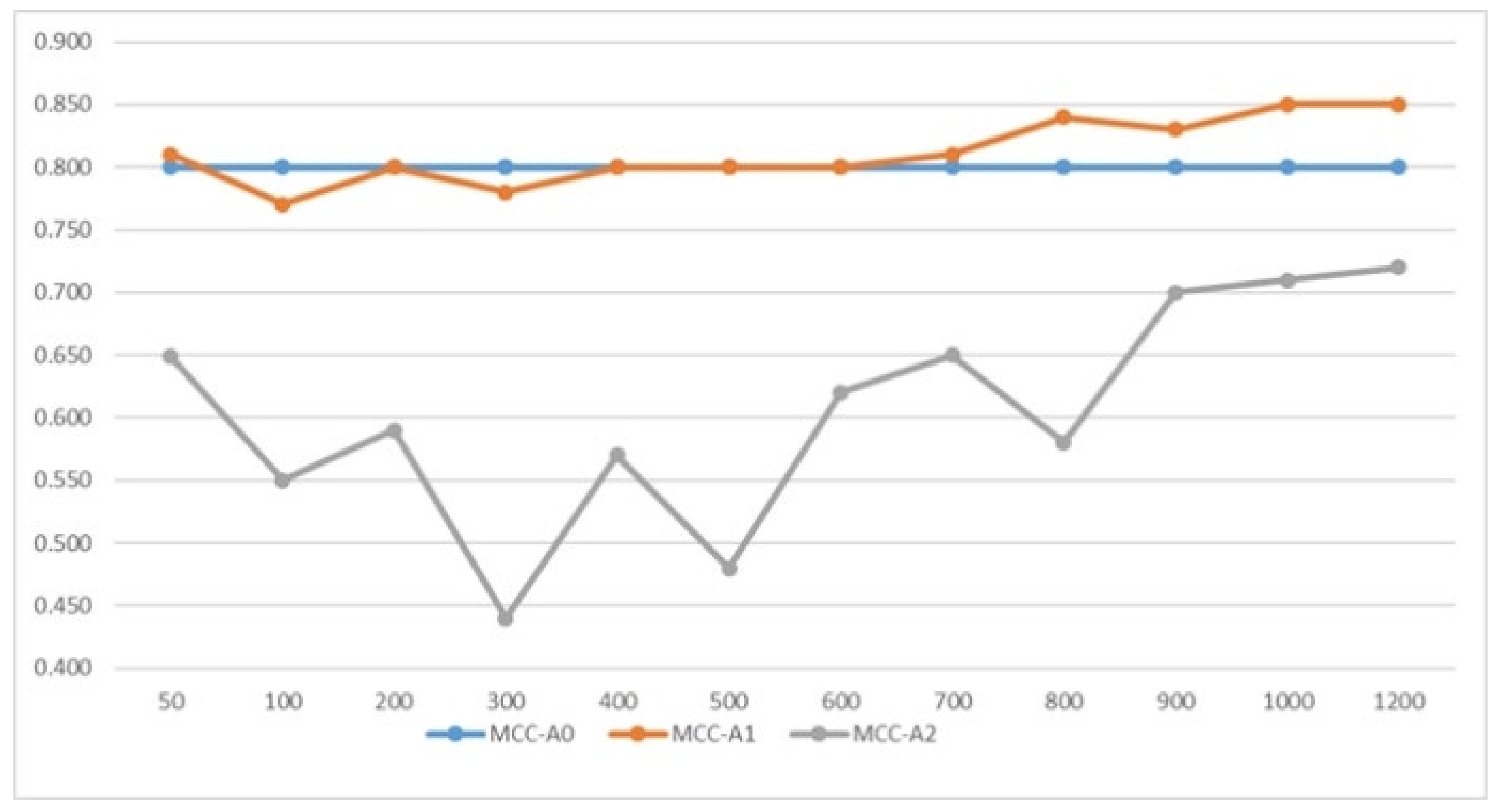
| Samples | F1 | MCC | Recall | Precision |
|---|---|---|---|---|
| 1200 | 0.87 | 0.80 | 0.85 | 0.89 |
| A1 | A2 | |||||||
|---|---|---|---|---|---|---|---|---|
| Samples | F1 | MCC | Recall | Precision | F1 | MCC | Recall | Precision |
| 50 | 0.88 | 0.81 | 0.87 | 0.89 | 0.81 | 0.65 | 0.98 | 0.69 |
| 100 | 0.82 | 0.77 | 0.89 | 0.76 | 0.77 | 0.55 | 0.94 | 0.65 |
| 200 | 0.86 | 0.80 | 0.82 | 0.90 | 0.77 | 0.59 | 0.92 | 0.66 |
| 300 | 0.87 | 0.78 | 0.88 | 0.86 | 0.68 | 0.44 | 0.76 | 0.61 |
| 400 | 0.87 | 0.80 | 0.83 | 0.91 | 0.76 | 0.57 | 0.89 | 0.67 |
| 500 | 0.88 | 0.80 | 0.85 | 0.91 | 0.74 | 0.48 | 0.94 | 0.61 |
| 600 | 0.88 | 0.80 | 0.87 | 0.89 | 0.74 | 0.62 | 0.86 | 0.65 |
| 700 | 0.88 | 0.81 | 0.87 | 0.89 | 0.79 | 0.65 | 0.88 | 0.72 |
| 800 | 0.90 | 0.84 | 0.91 | 0.89 | 0.76 | 0.58 | 0.83 | 0.70 |
| 900 | 0.89 | 0.83 | 0.89 | 0.89 | 0.79 | 0.70 | 0.84 | 0.74 |
| 1000 | 0.90 | 0.85 | 0.91 | 0.89 | 0.83 | 0.71 | 0.90 | 0.77 |
| 1200 | 0.90 | 0.85 | 0.91 | 0.89 | 0.84 | 0.72 | 0.93 | 0.77 |
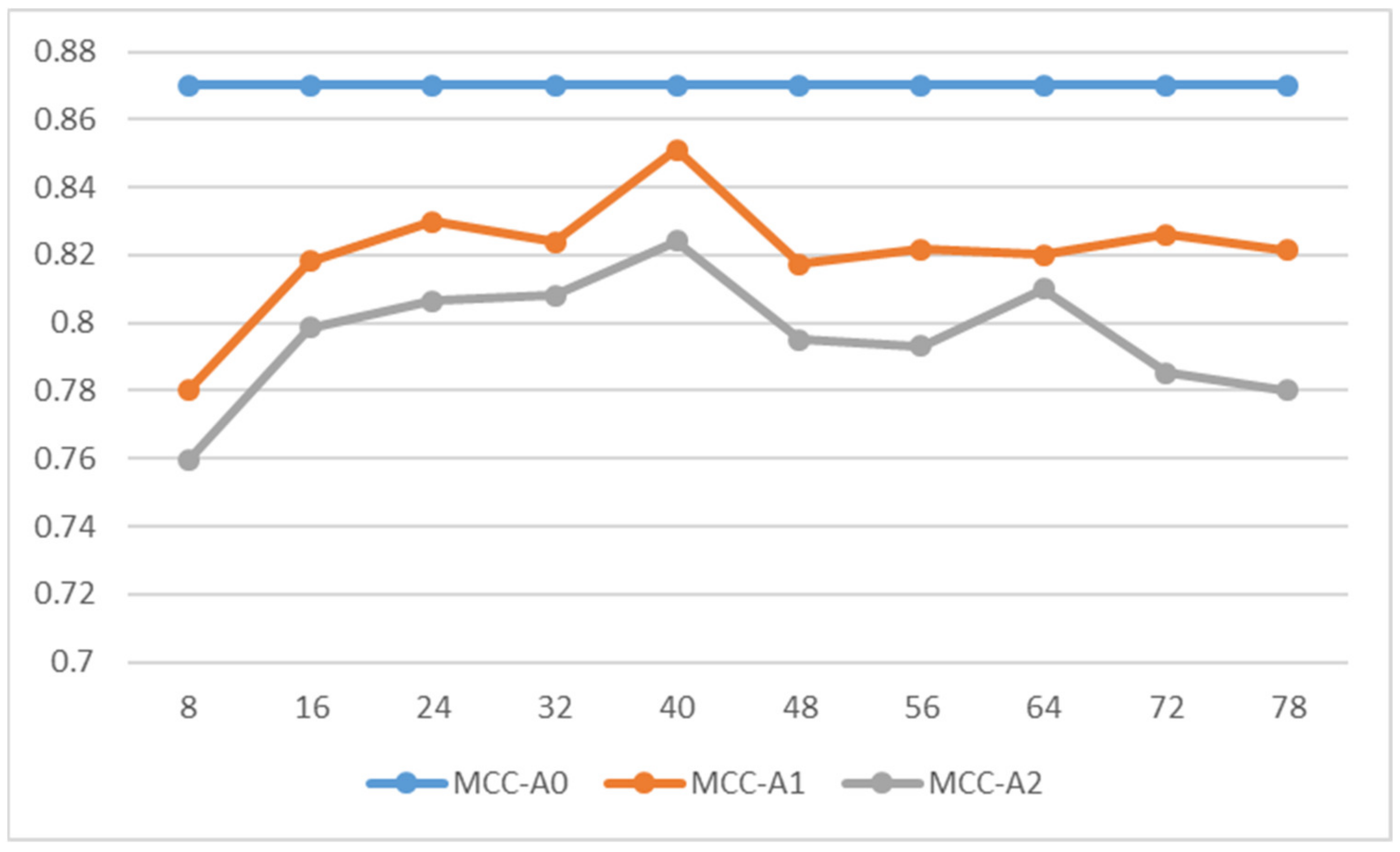
| Samples | F1 | MCC | Recall | Precision |
|---|---|---|---|---|
| 78 | 0.88 | 0.87 | 0.90 | 0.87 |
| A1 | A2 | |||||||
|---|---|---|---|---|---|---|---|---|
| Samples | F1 | MCC | Recall | Precision | F1 | MCC | Recall | Precision |
| 8 | 0.80 | 0.78 | 0.80 | 0.80 | 0.77 | 0.76 | 0.79 | 0.76 |
| 16 | 0.83 | 0.82 | 0.85 | 0.81 | 0.81 | 0.80 | 0.82 | 0.80 |
| 24 | 0.84 | 0.83 | 0.89 | 0.79 | 0.82 | 0.81 | 0.83 | 0.81 |
| 32 | 0.83 | 0.82 | 0.86 | 0.81 | 0.82 | 0.81 | 0.84 | 0.80 |
| 40 | 0.86 | 0.85 | 0.89 | 0.83 | 0.83 | 0.82 | 0.88 | 0.80 |
| 48 | 0.83 | 0.82 | 0.82 | 0.84 | 0.81 | 0.80 | 0.84 | 0.78 |
| 56 | 0.83 | 0.82 | 0.82 | 0.84 | 0.81 | 0.79 | 0.84 | 0.78 |
| 64 | 0.83 | 0.82 | 0.91 | 0.77 | 0.82 | 0.81 | 0.85 | 0.79 |
| 72 | 0.84 | 0.83 | 0.83 | 0.84 | 0.80 | 0.78 | 0.86 | 0.75 |
| 78 | 0.83 | 0.82 | 0.87 | 0.80 | 0.79 | 0.78 | 0.88 | 0.72 |
Publisher’s Note: MDPI stays neutral with regard to jurisdictional claims in published maps and institutional affiliations. |
© 2021 by the authors. Licensee MDPI, Basel, Switzerland. This article is an open access article distributed under the terms and conditions of the Creative Commons Attribution (CC BY) license (https://creativecommons.org/licenses/by/4.0/).
Share and Cite
Volkau, I.; Mujeeb, A.; Dai, W.; Erdt, M.; Sourin, A. The Impact of a Number of Samples on Unsupervised Feature Extraction, Based on Deep Learning for Detection Defects in Printed Circuit Boards. Future Internet 2022, 14, 8. https://0-doi-org.brum.beds.ac.uk/10.3390/fi14010008
Volkau I, Mujeeb A, Dai W, Erdt M, Sourin A. The Impact of a Number of Samples on Unsupervised Feature Extraction, Based on Deep Learning for Detection Defects in Printed Circuit Boards. Future Internet. 2022; 14(1):8. https://0-doi-org.brum.beds.ac.uk/10.3390/fi14010008
Chicago/Turabian StyleVolkau, Ihar, Abdul Mujeeb, Wenting Dai, Marius Erdt, and Alexei Sourin. 2022. "The Impact of a Number of Samples on Unsupervised Feature Extraction, Based on Deep Learning for Detection Defects in Printed Circuit Boards" Future Internet 14, no. 1: 8. https://0-doi-org.brum.beds.ac.uk/10.3390/fi14010008