Surrogate Assisted Optimization for Low-Voltage Low-Power Circuit Design


Abstract
:1. Introduction
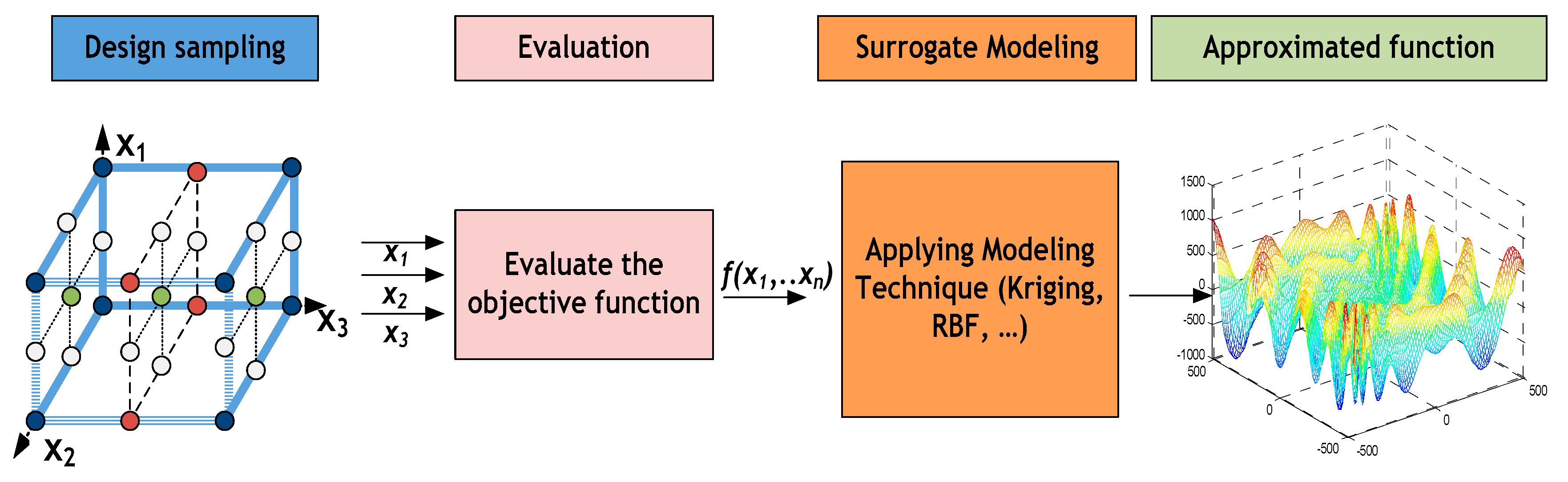
2. Metamodeling Technique: An Overview
3. The Optimization Kernel
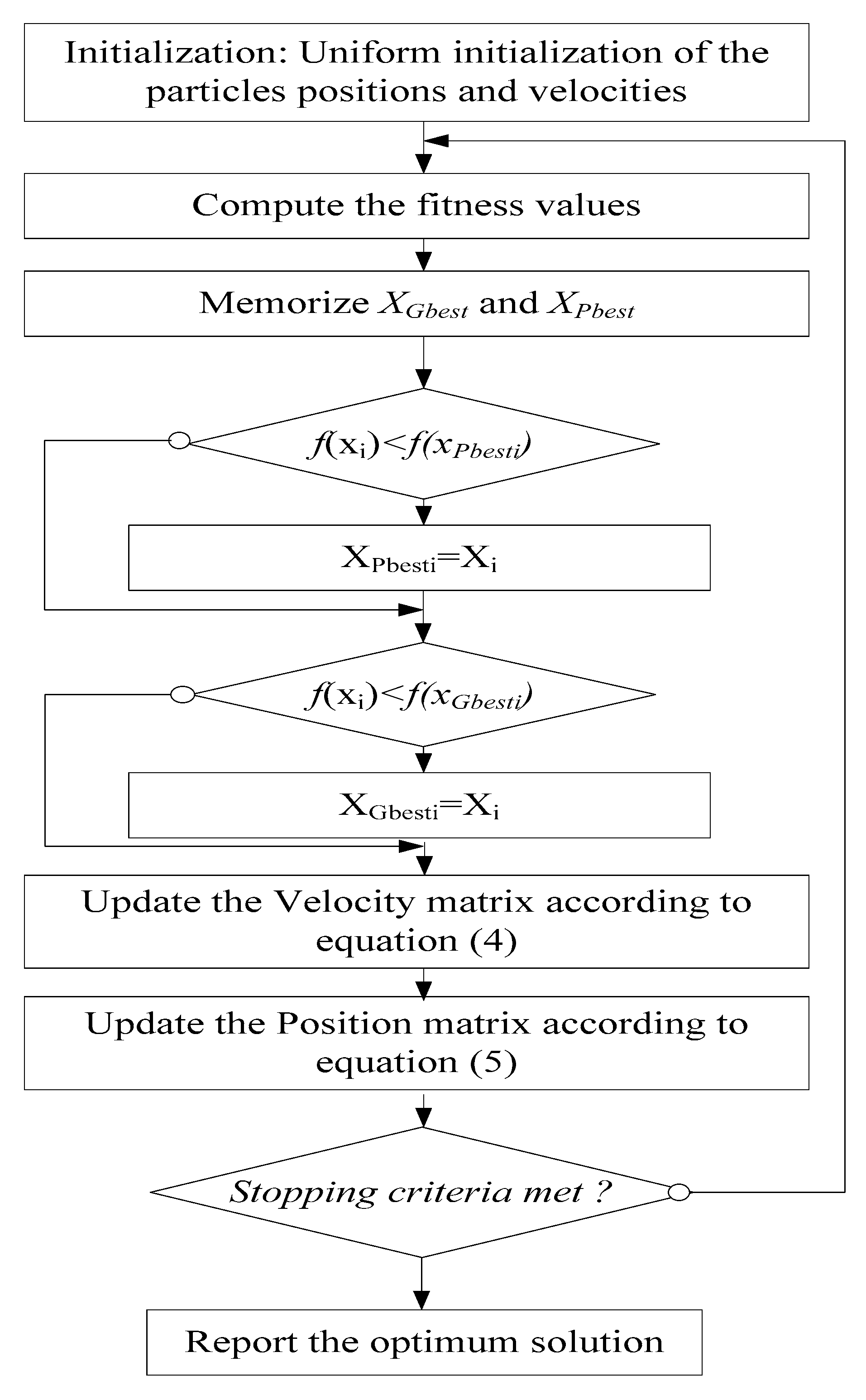
3.1. The Particle Swarm Optimization Algorithm
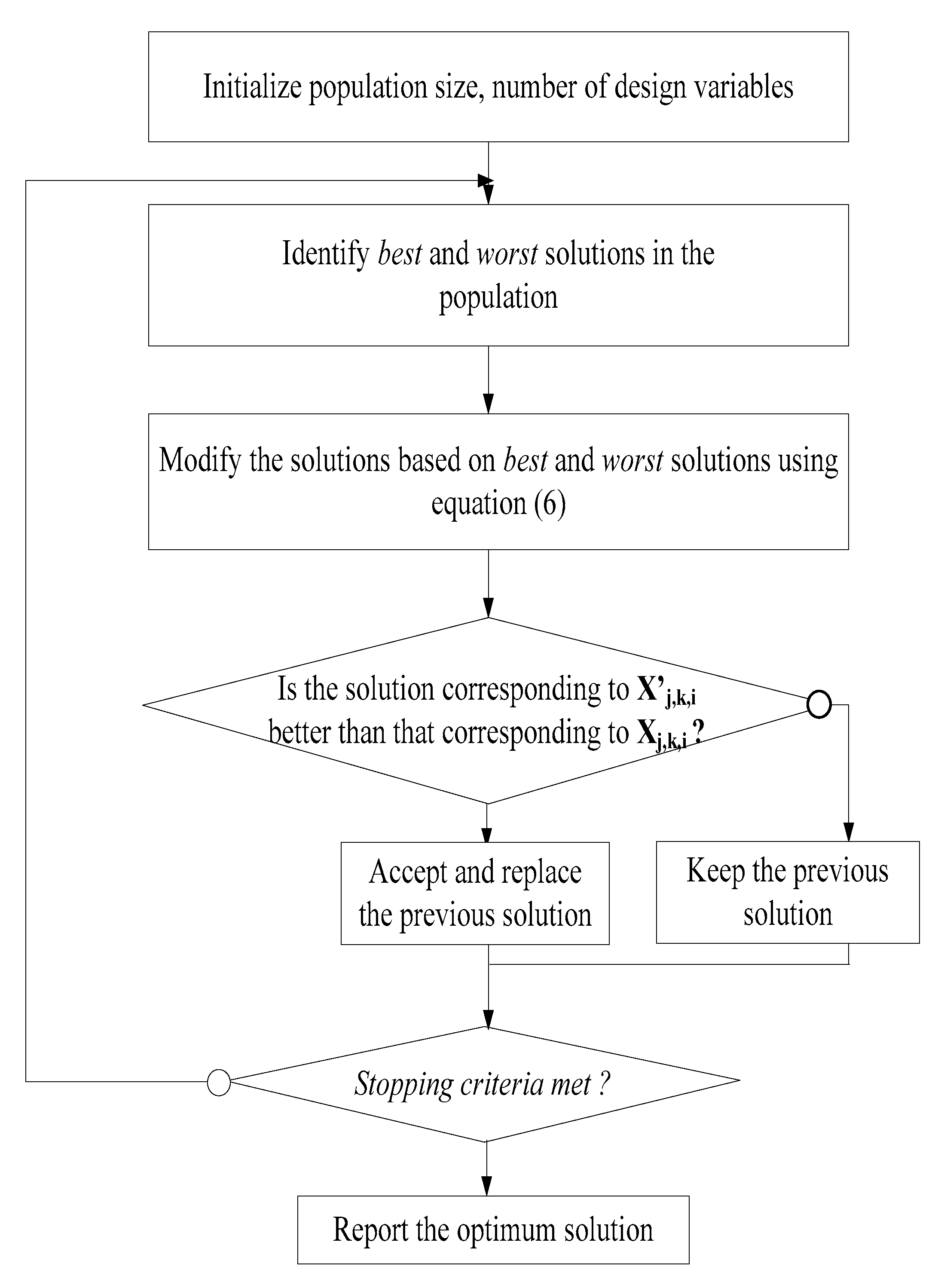
3.2. The JAYA Algorithm
4. The Proposed Approach and Application Examples
4.1. The Proposed Approach
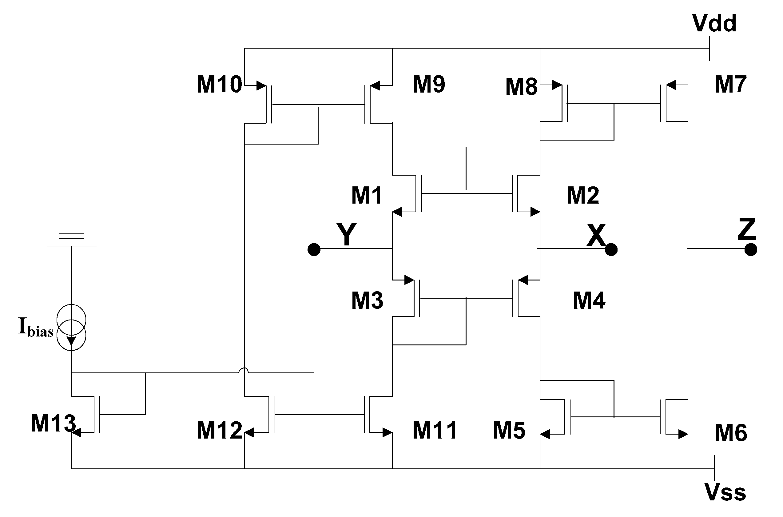
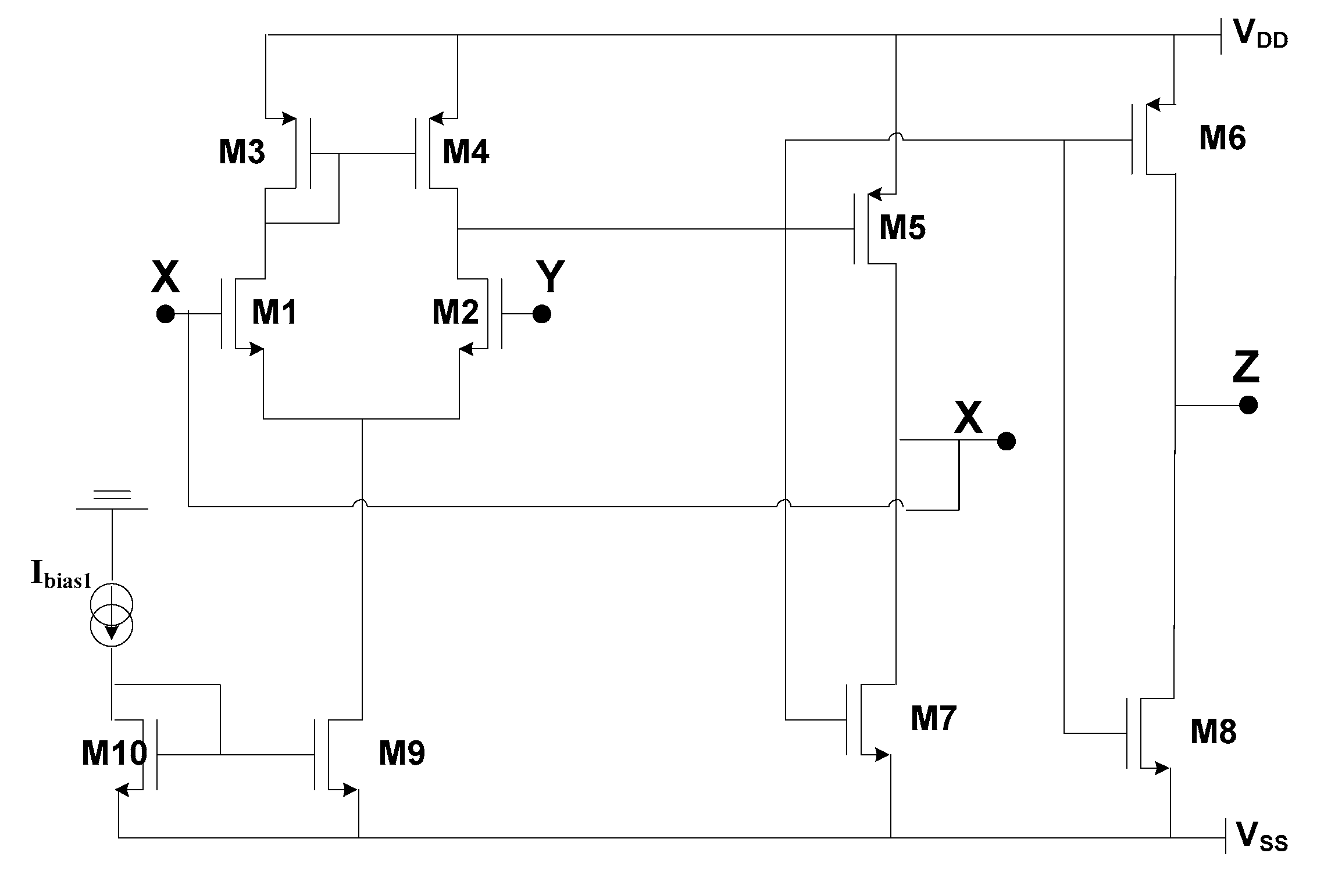
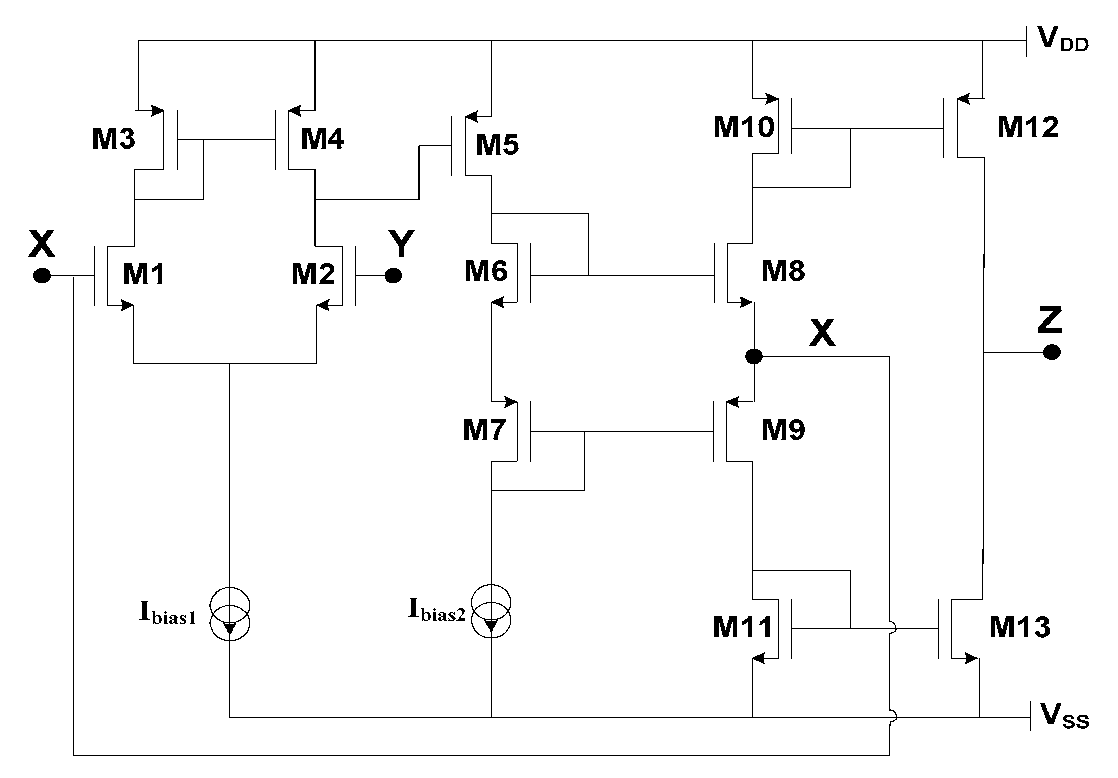
4.2. Application 1: A Class AB CMOS CCII+
4.3. Application 2: A Differential-Based Class AB CMOS CCII
4.4. Application 3: An CMOS OTA-Based CCII+
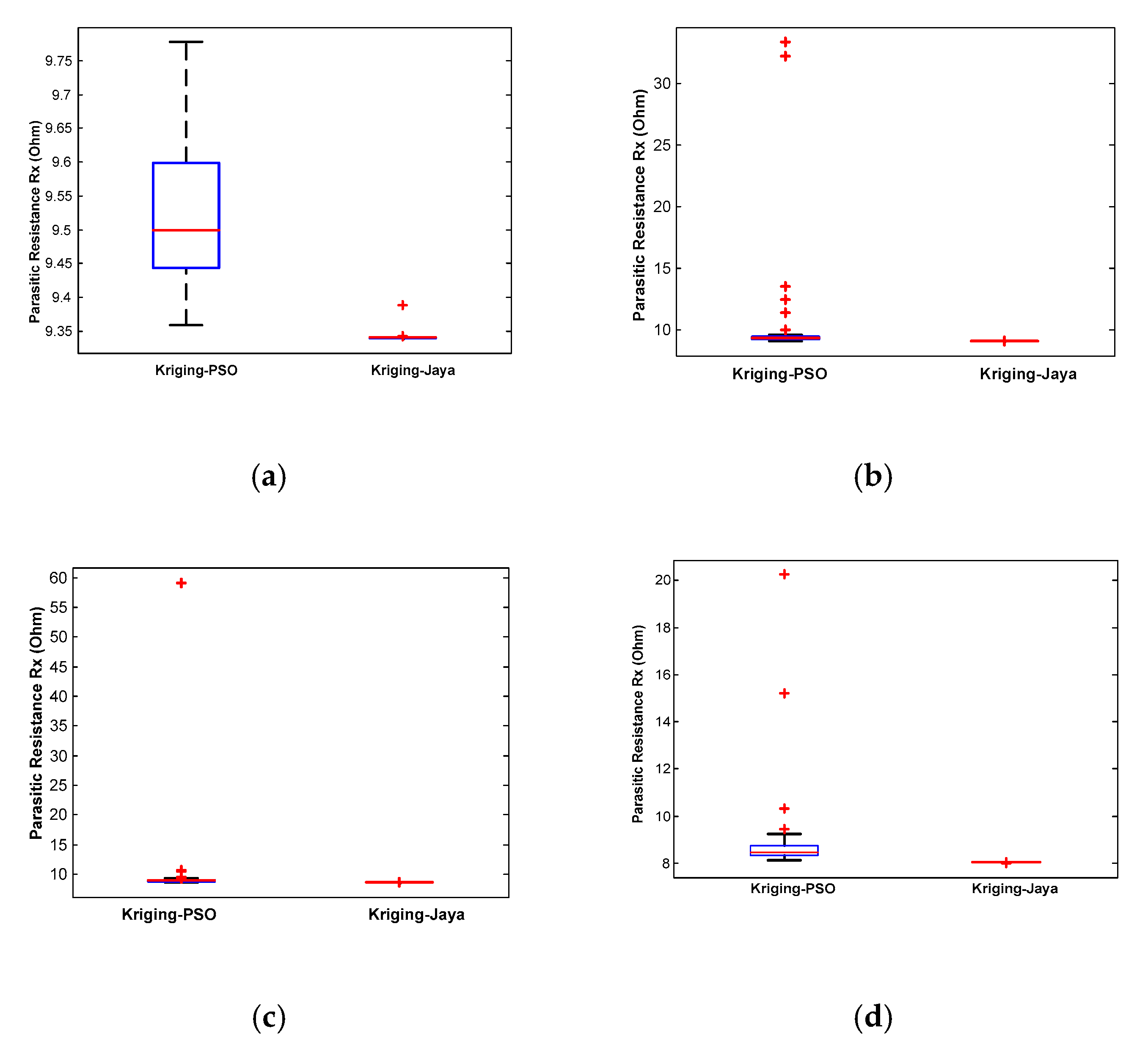
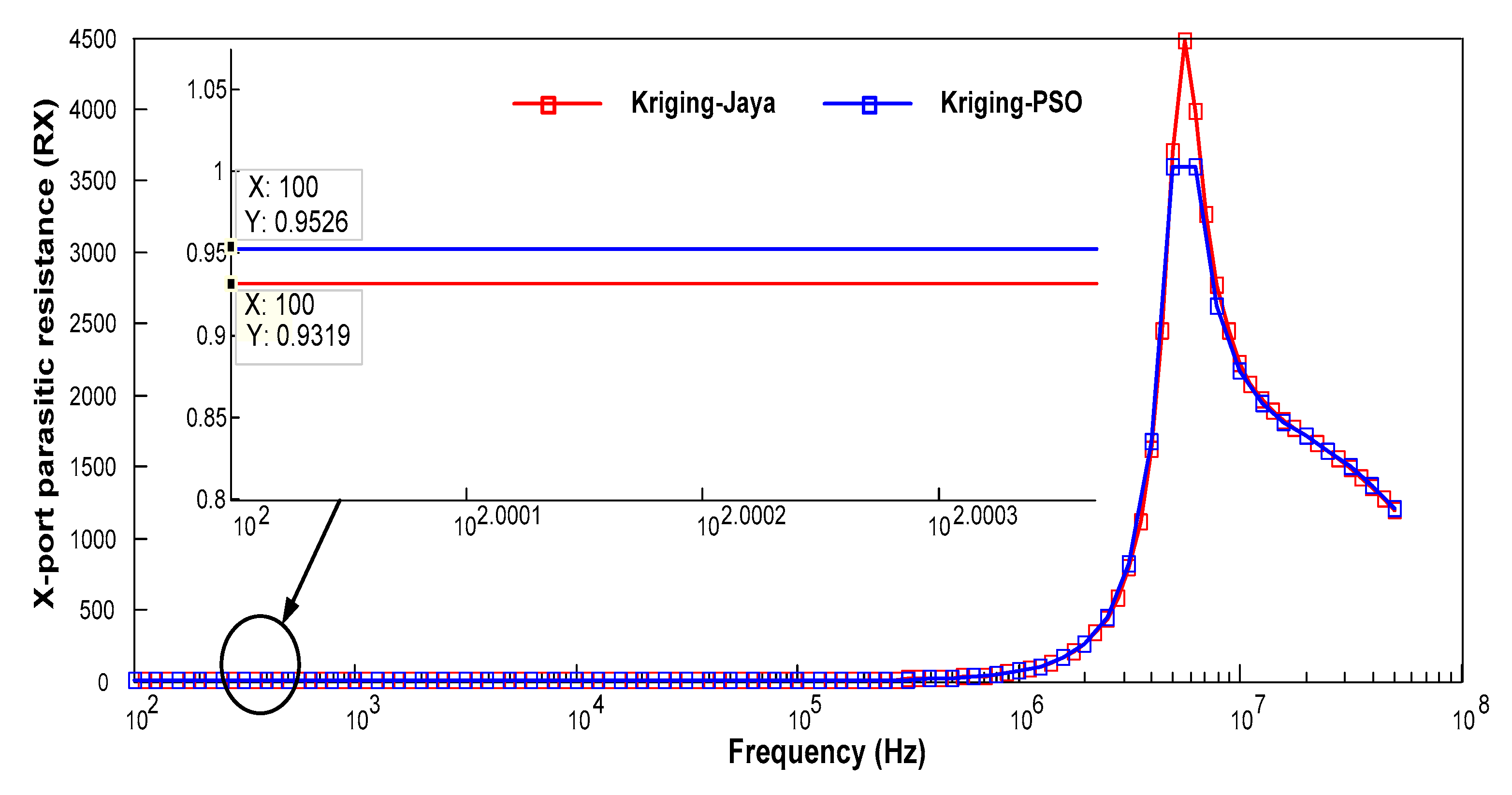
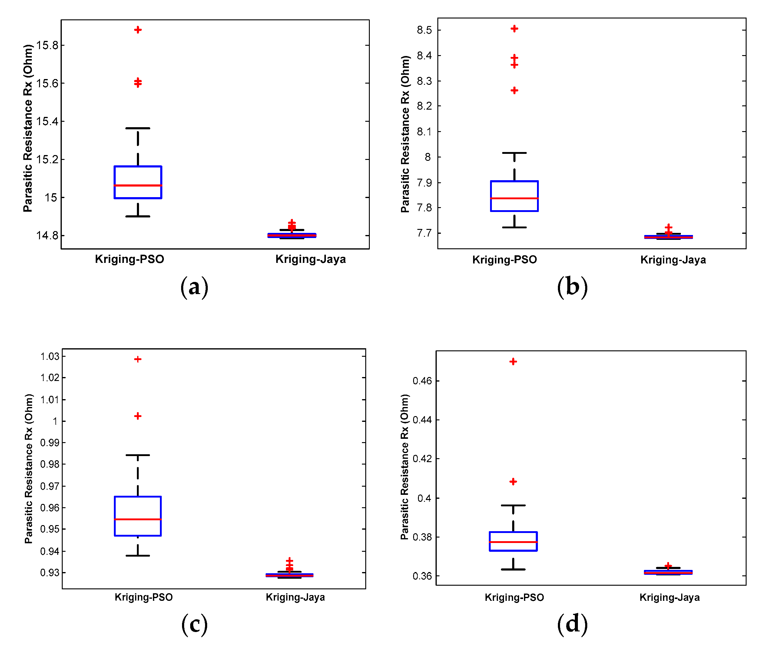
5. Comparisons and Discussion
6. Conclusions
Author Contributions
Funding
Conflicts of Interest
References
- Ferri, G.; Guerrini, N.C. CCII low voltage low power design and characteristics. In Low-Voltage Low-Power CMOS Current Conveyors; Ferri, G., Guerrini, N.C., Eds.; Springer: Boston, MA, USA, 2004; pp. 67–118. [Google Scholar]
- Elwan, H.O.; Soliman, A.M. Low-voltage low-power CMOS current conveyors. IEEE Trans. Circuits Syst.—I: Fundam. Theory Appl. 1997, 44, 828–835. [Google Scholar] [CrossRef]
- Ettaghzouti, T.; Hassen, N.; Besbes, K. A novel low-voltage low-power ccii based on super class AB CMOS OTA cells and filter application. In Proceedings of the 12th International Multi-Conference on Systems, Signals & Devices, Mahdia, Tunisia, 16–19 March 2015. [Google Scholar]
- Ettaghzouti, T.; Hassen, N.; Besbes, K. High performance low voltage low power voltage mode analog multiplier circuit. In Proceedings of the 7th International Conference on Sciences of Electronics, Technologies of Information and Telecommunications, Hammamet, Tunisia, 18–20 December 2016. [Google Scholar]
- Varun, N. A novel low power FGMOS-CCII based fully CMOS four quadrant multiplier. In Proceedings of the International Conference on Computing, Communication and Automation, Noida, India, 29–30 April 2016. [Google Scholar]
- Khateb, A.; Biolek, D.; Novacek, K. On the design of low-voltage low-power bulk-driven CMOS current conveyors. In Proceedings of the 29th International Spring Seminar on Electronics Technology, St. Marienthal, Germany, 10–14 May 2006. [Google Scholar]
- Ettaghzouti, T.; Hassen, N.; Besbes, K. Novel CMOS second generation current conveyor CCII with rail-to-rail input stage and filter application. In Proceedings of the 11th International Multi-Conference on Systems, Signals & Devices, Barcelona, Spain, 11–14 February 2014. [Google Scholar]
- Hamed, H.F.A.; Khalaf, A.A.M. 1 V supply second generation current conveyor in standard CMOS technology for low voltage low power analog circuits applications. In Proceedings of the 46th Midwest Symposium on Circuits and Systems, Cairo, Egypt, 27–30 December 2003. [Google Scholar]
- Sallem, A.; Guerra-Gómez, I.; Fakhfakh, M.; Loulou, M.; Tlelo-Cuautle, E. Simulation-based optimization of CCIIs’ performances in weak inversion. In Proceedings of the 17th IEEE International Conference on Electronics, Circuits and Systems, Athens, Greece, 12–15 December 2010. [Google Scholar]
- Ferri, G.; De Marcellis, A.; Di Carlo, C.; Stornelli, V.; Flammini, A.; Depari, A.; Marioli, D.; Sisinni, E. A CCII-based low-voltage low-power read-out circuit for dc-excited resistive gas sensors. IEEE Sens. J. 2009, 9, 2035–2041. [Google Scholar] [CrossRef]
- Ferri, G.; Guerrini, N. High-valued passive element simulation using low-voltage low-power current conveyors for fully integrated applications. IEEE Trans. Circuits Syst. —II: Analog Digit. Signal Process. 2001, 48, 405–409. [Google Scholar] [CrossRef]
- Ferri, G.; Guerrini, N.C. Low-voltage low-power novel CCII topologies and applications. In Proceedings of the 8th IEEE International Conference on Electronics, Circuits and Systems, Malta, Malta, 2–5 September 2001. [Google Scholar]
- Bhargave, G.; Sheokand, P.; Kaur, J. A new low voltage and low power filter using DTMOS-CCII. In Proceedings of the Second International Conference on Advances in Computing and Communication Engineering, Dehradun, India, 1–2 May 2015. [Google Scholar]
- Wang, A.; Calhoun, B.H.; Chandrakasan, A.P. Sub-Threshold Design for Ultra Low-Power Systems; Springer: Berlin, Germany, 2006. [Google Scholar]
- Garbaya, A.; Kotti, M.; Fakhfakh, M.; Siarry, P. The backtracking search for the optimal design of low-noise amplifiers. In Computational Intelligence in Analog and Mixed-Signal (AMS) and Radio-Frequency (RF) Circuit Design; Fakhfakh, M., Tlelo-Cuautle, E., Siarry, P., Eds.; Springer: Basel, Switzerland, 2015; pp. 391–412. [Google Scholar]
- Kotti, M.; Sallem, A.; Bougharriou, M.; Fakhfakh, M.; Loulou, M. Optimizing CMOS LNA circuits through multi-objective meta-heuristics. In Proceedings of the International Workshop on Symbolic and Numerical Methods, Modeling and Applications to Circuit Design, Gammarth, Tunisia, 4–6 October 2010. [Google Scholar]
- Neoh, S.C.; Marzuki, A.; Morad, N.; Lim, C.P.; Aziz, Z.A. An Interactive evolutionary algorithm for MMIC low noise amplifier design. ICIC Express Lett. 2009, 3, 15–19. [Google Scholar]
- González-Echevarría, R.; Roca, E.; Castro-López, R.; Fernández, F.V.; Sieiro, J.; López-Villegas, J.M.; Vidal, N. An automated design methodology of RF circuits by using Pareto-optimal fronts of EM simulated inductors. IEEE Trans. Comput.—Aided Des. Integr. Circuits Syst. 2016, 36, 15–26. [Google Scholar]
- Passos, F.; González-Echevarria, R.; Roca, E.; Castro-López, R.; Fernández, F.V. A two-step surrogate modeling strategy for single-objective and multi-objective optimization of radiofrequency circuits, methodologies and application. Soft Comput. 2019, 23, 4911–4925. [Google Scholar] [CrossRef] [Green Version]
- Li, Y.; Yu, S.M.; Li, Y.L. A simulation-based hybrid optimization technique for low noise amplifier design automation. In Proceedings of the International Conference on Computational Science, Beijing, China, 27–30 May 2007. [Google Scholar]
- Garbaya, A.; Kotti, M.; Drira, N.; Fakhfakh, M.; Tlelo-Cuautle, E.; Siarry, P. An RBF-PSO technique for the rapid optimization of (CMOS) analog circuits. In Proceedings of the International Conference on Modern Circuits and Systems Technologies, Thessaloniki, Greece, 7–9 May 2018. [Google Scholar]
- Box, G.E.P.; Wilson, K.B. On the experimental attainment of optimum conditions. J. R. Stat. Soc. 1951, 13, 1–45. [Google Scholar] [CrossRef]
- Krige, D.G. A statistical approach to some basic mine valuation problems on the Witwatersrand. J. Chem. Metall. Min. Soc. South Afr. 1953, 52, 119–139. [Google Scholar]
- Hardy, R.L. Multiquadratic Equations of Topography and Other Irregular Surfaces. J. Geophys. Res. 1971, 76, 1905–1915. [Google Scholar] [CrossRef]
- Lourenço, J.M.; Lebensztajn, L. Surrogate modeling and two level infill criteria applied to electromagnetic device optimization. IEEE Trans. Magn. 2015, 51, 34–42. [Google Scholar] [CrossRef]
- Zhao, D.; Xue, D. A multi-surrogate approximation method for metamodeling. Eng. Comput. 2011, 27, 139–153. [Google Scholar] [CrossRef]
- Kotti, M.; González-Echevarría, R.; Fernández, F.V.; Roca, E.; Sieiro, J.; Castro-López, R.; Fakhfakh, M.; López-Villegas, J.M. Generation of surrogate models of Pareto-optimal performance trade-offs of planar inductors. Analog Integr. Circuits Signal Process. 2014, 78, 87–97. [Google Scholar] [CrossRef]
- Garbaya, A.; Kotti, M.; Fakhfakh, M.; BenHala, B. Comparative study of Jaya metaheuristic to benchmark functions and RF circuits. In Proceedings of the International Conference on Innovative Research in Applied Science, Engineering and Technology, Fes, Morocco, 19–20 March 2020. [Google Scholar]
- Rao, R.V. Jaya: A simple and new optimization algorithm for solving constrained and unconstrained optimization problems. Int. J. Ind. Eng. Comput. 2016, 7, 19–34. [Google Scholar]
- Garbaya, A.; Kotti, M.; Fakhfakh, M.; Tlelo-Cuautle, E. On the accurate modeling of analog circuits via the kriging metamodeling technique. In Proceedings of the International Conference on Synthesis, Modeling, Analysis and Simulation Methods and Applications to Circuit Design, Giardini Naxos, Italy, 12–15 June 2017. [Google Scholar]
- Garbaya, A.; Kotti, M.; Fakhfakh, M. Radial basis function surrogate modeling for the accurate design of analog circuits. In Analog Circuits: Fundamentals, Synthesis and Performance; Tlelo-Cuautle, E., Fakhfakh, M., De La Fraga, L.G., Eds.; Nova: New York, NY, USA, 2017; pp. 269–286. [Google Scholar]
- Koziel, S.; Pietrenko-Dabrowska, A. Performance-based nested surrogate modeling of antenna input characteristics. IEEE Trans. Antennas Propag. 2019, 67, 2904–2912. [Google Scholar] [CrossRef]
- Koziel, S.; Bekasiewicz, A.; Szczepanski, S. Multi-objective design optimization of antennas for reflection, size, and gain variability using kriging surrogates and generalized domain segmentation. Int. J. Rf Microw. Comput.—Aided Eng. 2018, 28, 1–11. [Google Scholar] [CrossRef]
- Koziel, S.; Pietrenko-Dabrowska, A. Rapid multi-objective optimization of antennas using nested kriging surrogates and single-fidelity EM simulation models. Eng. Comput. 2019, 37, 1491–1512. [Google Scholar] [CrossRef]
- Fakhfakh, M.; Tlelo-Cuautle, E.; Siarry, P. Computational Intelligence in Analog and Mixed-Signal (AMS) and Radio-Frequency (RF) Circuit Design; Springer: Basel, Switzerland, 2015. [Google Scholar]
- Siarry, P.; Michalewicz, Z. Advances in Metaheuristics for Hard Optimization; Springer: Berlin, Germany, 2007. [Google Scholar]
- Barros, M.F.; Guilherme, J.; Horta, N. Analog Circuits and Systems Optimization Based on Evolutionary Computation Techniques; Springer: Berlin, Germany, 2010. [Google Scholar]
- Goldberg, D.E.; Richardson, J. Genetic algorithms with sharing for multimodal function optimization, Genetic algorithms and their applications. In Proceedings of the International Conference on Genetic Algorithms; Lawrence Erlbaum Associates Inc.: Hillsdale, NJ, USA, 1987. [Google Scholar]
- Dorigo, M.; Birattari, M.; Stutzle, T. Ant colony optimization. IEEE Comput. Intell. Mag. 2006, 1, 28–39. [Google Scholar] [CrossRef]
- Passino, K.M. Biomimicry of bacterial foraging for distributed optimization and control. IEEE Control. Syst. Mag. 2002, 22, 52–67. [Google Scholar]
- Gandomi, A.H.; Yang, X.S.; Alavi, A.H. Mixed variable structural optimization using Firefly Algorithm. Comput. Struct. 2011, 89, 2325–2336. [Google Scholar] [CrossRef]
- Basu, M. A simulated annealing-based goal-attainment method for economic emission load dispatch of fixed head hydrothermal power systems. Int. J. Electr. Power Energy Syst. 2005, 27, 147–153. [Google Scholar] [CrossRef]
- Clerc, M. Particle Swarm Optimization; International Scientific and Technical Encyclopaedia: London, UK, 2006. [Google Scholar]
- Sallem, A.; BenHala, B.; Kotti, M.; Fakhfakh, M.; Ahaitouf, A.; Loulou, M. Application of swarm intelligence techniques to the design of analog circuits: Evaluation and comparison. Analog Integr. Circuits Signal Process. 2013, 75, 499–516. [Google Scholar] [CrossRef]
- Michailidis, P.D. An efficient multi-core implementation of the Jaya optimisation algorithm. Int. J. Parallel Emergent Distrib. Syst. 2017, 34, 288–320. [Google Scholar] [CrossRef]
- Pandey, H.M. Jaya a novel optimization algorithm: What, how and why? In Proceedings of the 6th International Conference—Cloud System and Big Data Engineering (Confluence), Noida, India, 14–15 January 2016. [Google Scholar]
- Rao, R.V.; Rai, D.P.; Balic, J. Optimization of abrasive water jet machining process using multi-objective Jaya algorithm. Mater. Today: Proc. 2018, 5, 4930–4938. [Google Scholar]
- Rao, R.V.; Rai, D.P.; Ramkumar, J.; Balic, J. A new multi-objective Jaya algorithm for optimization of modern machining processes. Adv. Prod. Eng. Manag. 2016, 11, 271–286. [Google Scholar] [CrossRef] [Green Version]
- Ferri, G.; Guerrini, N. Low-Voltage Low-Power CMOS Current Conveyors; Springer: Boston, MA, USA, 2003. [Google Scholar]
- Forrester, A.I.J.; Sobester, A.; Keane, A. Engineering Design via Surrogate Modelling; A Practical Guide; Wiley: Pondicherry, India, 2008. [Google Scholar]
- Civicioglu, P. Backtracking search optimization algorithm for numerical optimization problems. Appl. Math. Comput. 2013, 219, 8121–8144. [Google Scholar] [CrossRef]


| Ibiais (µA) | Relative Error (%) |
|---|---|
| 15 | 0.042 |
| 20 | 0.046 |
| 26 | 0.005 |
| 30 | 0.007 |
| 45 | 0.009 |
| Ibiais (µA) | Ln (µm) | Wn (µm) | Lp (µm) | Wp (µm) | Optimized Rx (Ω) | Simulated Rx (Ω) | Relative Error (%) | |
|---|---|---|---|---|---|---|---|---|
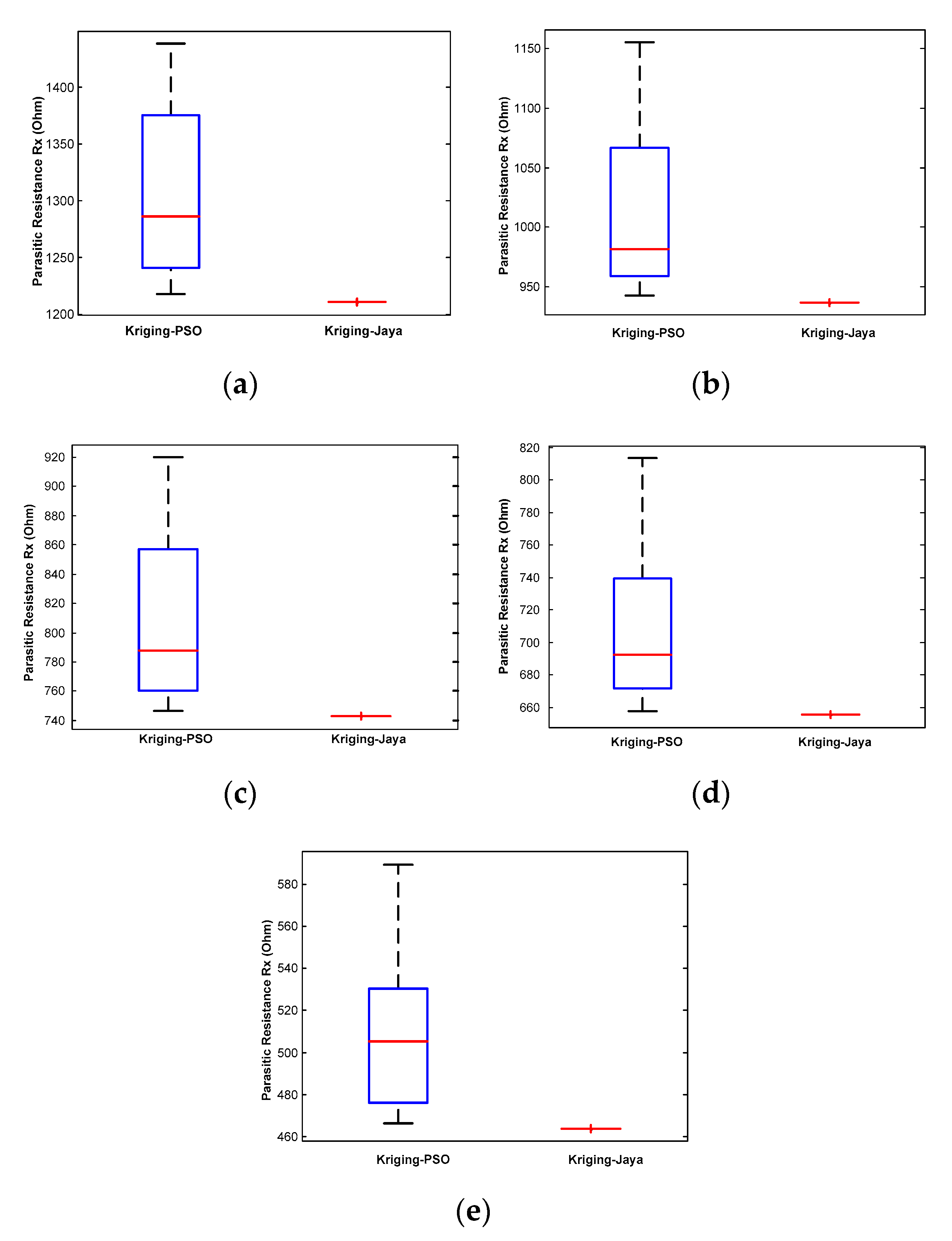
| Kriging-PSO | 15 | 0.746 | 318.810 | 0.644 | 499.340 | 1242.500 | 1240.800 | 0.137 |
| 20 | 0.751 | 324.456 | 0.641 | 498.337 | 962.780 | 960.070 | 0.282 | |
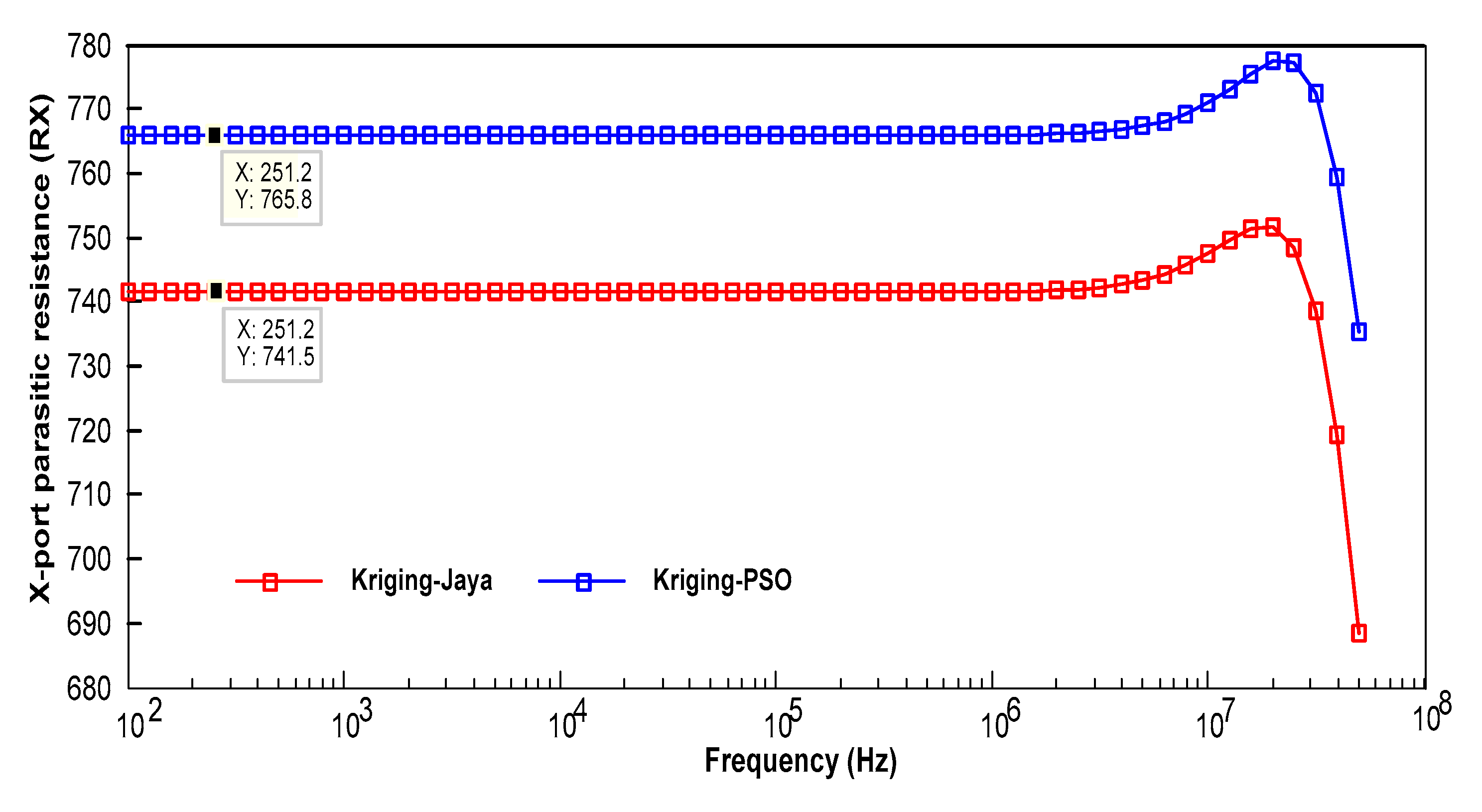
| 26 | 0.834 | 276.812 | 0.689 | 500.000 | 764.250 | 765.820 | 0.205 | |
| 30 | 0.746 | 318.629 | 0.644 | 499.351 | 673.974 | 673.470 | 0.074 | |
| 45 | 0.503 | 453.117 | 0.546 | 497.754 | 476.360 | 476.350 | 0.002 | |
| Kriging-Jaya | 15 | 0.663 | 499.910 | 0.665 | 500.000 | 1211.400 | 1208.000 | 0.281 |
| 20 | 0.681 | 496.242 | 0.667 | 500.000 | 936.972 | 934.490 | 0.265 | |
| 26 | 0.713 | 498.740 | 0.665 | 500.000 | 743.120 | 741.480 | 0.221 | |
| 30 | 0.715 | 499.375 | 0.664 | 500.000 | 655.792 | 654.434 | 0.207 | |
| 45 | 0.714 | 500.000 | 0.664 | 500.000 | 463.960 | 462.938 | 0.220 |
| Ibiais (µA) | Relative Error (%) |
|---|---|
| 0.10 | 0.829 |
| 0.25 | 0.386 |
| 1 | 0.092 |
| 10 | 0.007 |
| Ibiais (µA) | Ln (µm) | Wn (µm) | Lp (µm) | Wp (µm) | Optimized Rx (Ω) | Simulated Rx (Ω) | Relative Error (%) | |
|---|---|---|---|---|---|---|---|---|
| Kriging- PSO | 0.10 | 693.521 | 31.530 | 848.132 | 746.120 | 9.265 | 9.487 | 2.340 |
| 0.25 | 444.361 | 32.237 | 769.656 | 261.891 | 9.946 | 10.084 | 1.360 | |
| 1 | 283.484 | 30.710 | 832.148 | 124.233 | 9.037 | 8.953 | 0.930 | |
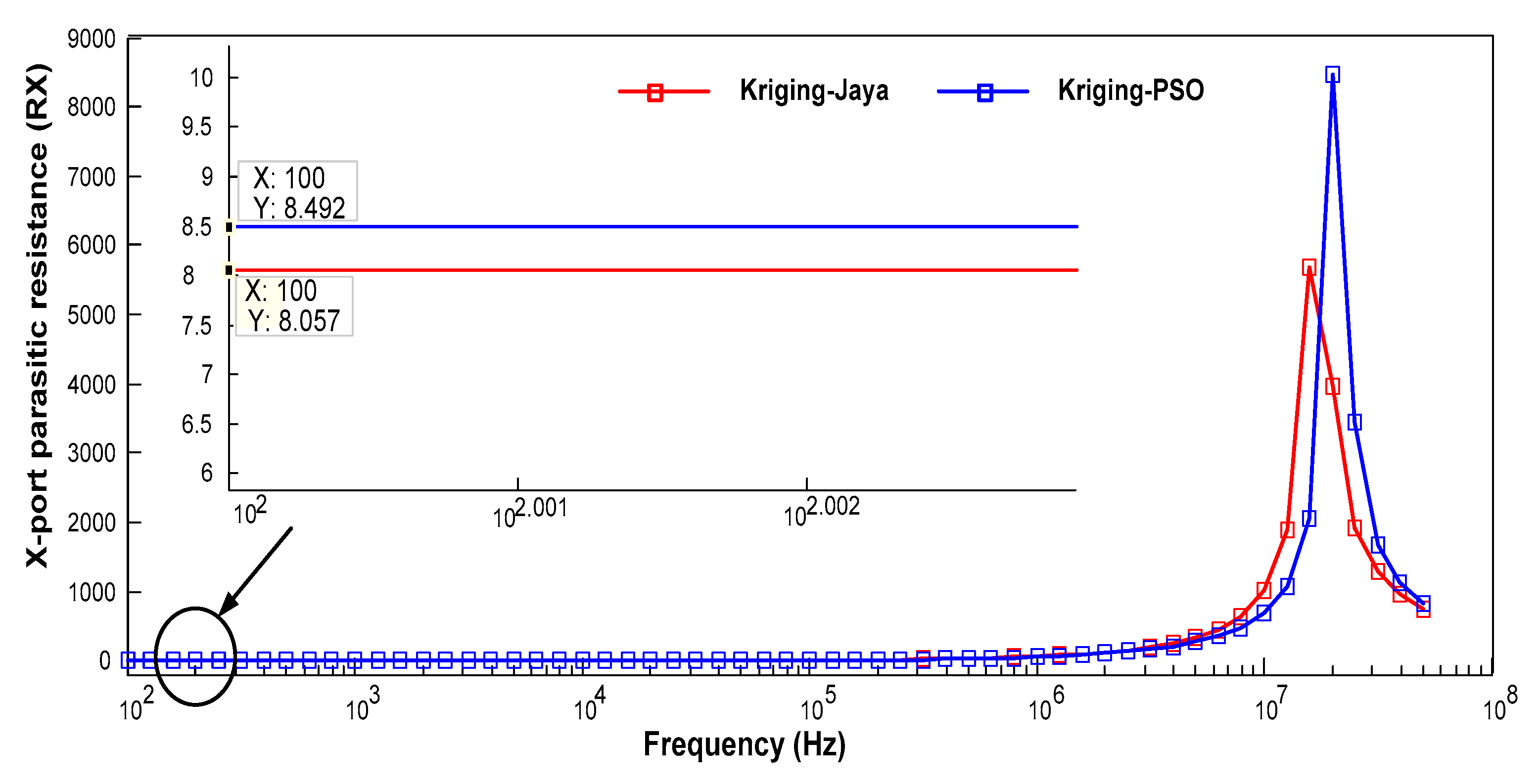
| 10 | 498.060 | 31.583 | 824.740 | 276.939 | 8.530 | 8.492 | 0.450 | |
| Kriging- JAYA | 0.10 | 99.160 | 35.000 | 849.576 | 474.915 | 9.340 | 9.377 | 0.400 |
| 0.25 | 562.035 | 26.702 | 849.958 | 451.720 | 9.093 | 9.088 | 0.050 | |
| 1 | 648.526 | 33.385 | 849.958 | 49.618 | 8.662 | 8.750 | 1.000 | |
| 10 | 850.000 | 27.006 | 849.958 | 48.875 | 8.050 | 8.057 | 0.090 |
| Ibiais2 (µA) | Relative Error (%) |
|---|---|
| 0.5 | 0.365 |
| 1 | 0.366 |
| 10 | 0.507 |
| 30 | 0.378 |
| Ibiais2 (µA) | Ln (µm) | Wn (µm) | Lp (µm) | Wp (µm) | Optimized Rx (Ω) | Simulated Rx (Ω) | Relative Error (%) | |
|---|---|---|---|---|---|---|---|---|
| Kriging- PSO | 0.5 | 385.211 | 13.468 | 377.879 | 401.654 | 15.000 | 15.007 | 0.047 |
| 1 | 333.942 | 11.767 | 360.872 | 365.650 | 7.817 | 7.802 | 0.191 | |
| 10 | 402.660 | 17.227 | 418.236 | 417.988 | 0.947 | 0.952 | 0.493 | |
| 30 | 437.826 | 11.018 | 403.388 | 371.282 | 0.367 | 0.369 | 0.515 | |
| Kriging- JAYA | 0.5 | 356.367 | 11.297 | 440.913 | 404.515 | 14.802 | 14.830 | 0.189 |
| 1 | 347.074 | 11.384 | 441.399 | 422.708 | 7.681 | 7.698 | 0.220 | |
| 10 | 343.585 | 11.572 | 448.640 | 417.206 | 0.928 | 0.932 | 0.429 | |
| 30 | 356.406 | 11.419 | 443.569 | 411.998 | 0.362 | 0.364 | 0.549 |
| Ibias | Vdd/Vss | Kriging-PSO | Kriging-JAYA | [9] | [49] | |
|---|---|---|---|---|---|---|
| Application #1 | 26 µA | ± 1 V | 765.82 Ω | 741.48 Ω | 725.00 Ω | 990.00 Ω |
| Application #2 | 10 µA | ± 0.6 V | 8.50 Ω | 8.06 Ω | 8.50 Ω | 12.00 Ω |
| Application #3 | 10 µA | ± 1 V | 0.95 Ω | 0.93 Ω | 0.90 Ω | 1.30 Ω |
| Computation Time (s) | -- | -- | 3.69 | 3.88 | 400.00 | -- |
| JAYA vs. PSO | p-Value | T+ | T- | Winner |
|---|---|---|---|---|
| Application #1 | 7.5569 × 10⁻¹⁰ | 0 | 50 | Jaya |
| Application #2 | 7.5569 × 10⁻¹⁰ | 0 | 50 | Jaya |
| Application #3 | 7.5569 × 10⁻¹⁰ | 0 | 50 | Jaya |
© 2020 by the authors. Licensee MDPI, Basel, Switzerland. This article is an open access article distributed under the terms and conditions of the Creative Commons Attribution (CC BY) license (http://creativecommons.org/licenses/by/4.0/).
Share and Cite
Garbaya, A.; Kotti, M.; Fakhfakh, M.; Tlelo-Cuautle, E. Surrogate Assisted Optimization for Low-Voltage Low-Power Circuit Design. J. Low Power Electron. Appl. 2020, 10, 20. https://0-doi-org.brum.beds.ac.uk/10.3390/jlpea10020020
Garbaya A, Kotti M, Fakhfakh M, Tlelo-Cuautle E. Surrogate Assisted Optimization for Low-Voltage Low-Power Circuit Design. Journal of Low Power Electronics and Applications. 2020; 10(2):20. https://0-doi-org.brum.beds.ac.uk/10.3390/jlpea10020020
Chicago/Turabian StyleGarbaya, Amel, Mouna Kotti, Mourad Fakhfakh, and Esteban Tlelo-Cuautle. 2020. "Surrogate Assisted Optimization for Low-Voltage Low-Power Circuit Design" Journal of Low Power Electronics and Applications 10, no. 2: 20. https://0-doi-org.brum.beds.ac.uk/10.3390/jlpea10020020