Article

High-Frequency Low-Current Second-Order Bandpass Active Filter Topology and Its Design in 28-nm FD-SOI CMOS

DIEEI (Dipartimento di Ingegneria Elettrica Elettronica e Informatica), University of Catania, 95125 Catania, Italy
*
Author to whom correspondence should be addressed.
J. Low Power Electron. Appl. 2020, 10(3), 27; https://0-doi-org.brum.beds.ac.uk/10.3390/jlpea10030027
Submission received: 27 July 2020 / Revised: 26 August 2020 / Accepted: 1 September 2020 / Published: 3 September 2020
(This article belongs to the Special Issue Low-Power CMOS Analog and Digital Circuits and Filters)

Abstract

:
Fully Depleted Silicon on Insulator (FD-SOI) CMOS technology offers the possibility of circuit performance optimization with reduction of both topology complexity and power consumption. These advantages are fully exploited in this paper in order to develop a new topology of active continuous-time second-order bandpass filter with maximum resonant frequency in the range of 1 GHz and wide electrically tunable quality factor requiring a very limited quiescent current consumption below 10 μA. Preliminary simulations that were carried out using the 28-nm FD-SOI technology from STMicroelectronics show that the designed example can operate up to 1.3 GHz of resonant frequency with tunable Q ranging from 90 to 370, while only requiring 6 μA standby current under 1-V supply.

1. Introduction

Fully Depleted Silicon on Insulator (FD-SOI) CMOS technologies provide several advantages in comparison to bulk CMOS, namely: (1) unparallel threshold voltage tuning range from the back gate, which allows effective trimming strategies for process and temperature compensation, (2) better threshold voltage matching, (3) low parasitic capacitances, (4) high transition frequency, fT, of hundreds of gigahertz, and (5) improved intrinsic dc gain [1]. These behaviors, together with the increased flexibility offered by the MOS “fourth terminal”, have enabled many ingenious and innovative integrated-circuit (IC) solutions in analog, radio frequency (RF), millimeter wave (mW), and mixed-signal systems also for automotive, IoT, 5G, and emerging applications [2,3,4,5].
Ubiquitous RF portable communications need ultra-low-power IC solutions that are able to prolong battery life and recharging cycles in energy harvested devices [6,7,8]. In these applications fundamental building blocks are continuous-time filters with tunable cutoff frequency and small fractional bandwidth. At this purpose, several IC implementations have been developed that exploit inductors, transformers, resonators, transmission lines, etc. [9,10,11,12,13,14,15,16]. These solutions usually require current consumptions in the order of several milliamperes in order to provide the required high frequency performance and frequently exploit nonstandard approaches for the CMOS technology.
This paper addresses the problem of designing a monolithic inductorless second-order band-pass active filter that is suitable for RF portable applications providing electrical tunability of both the resonant frequency and quality factor, under a very limited quiescent current budget constraint of a few microamperes. This result is achieved thanks to the low parasitic capacitances and high fT offered by the FD-SOI CMOS technology and through the extensive use, as a design option, of the body terminals of transistor devices [17,18,19]. No particular application has been targeted, as the purpose of this document is simply to introduce a new topology and show its potential. To this end, a preliminary design example was developed and simulated while using STMicroelectronics 28-nm process. The filter consumes 6 μA of dc current from a single 1-V power supply while providing a resonant frequency of 1.3 GHz and tunable quality factor ranging from 90 to 370. Simulated 1-dB compression point, P1dB, and input referred third-order intercept point, IIP3, were −20.5 dBm and −9.23 dBm, respectively. The noise Figure was found to be 31 dB.

2. The Proposed Solution

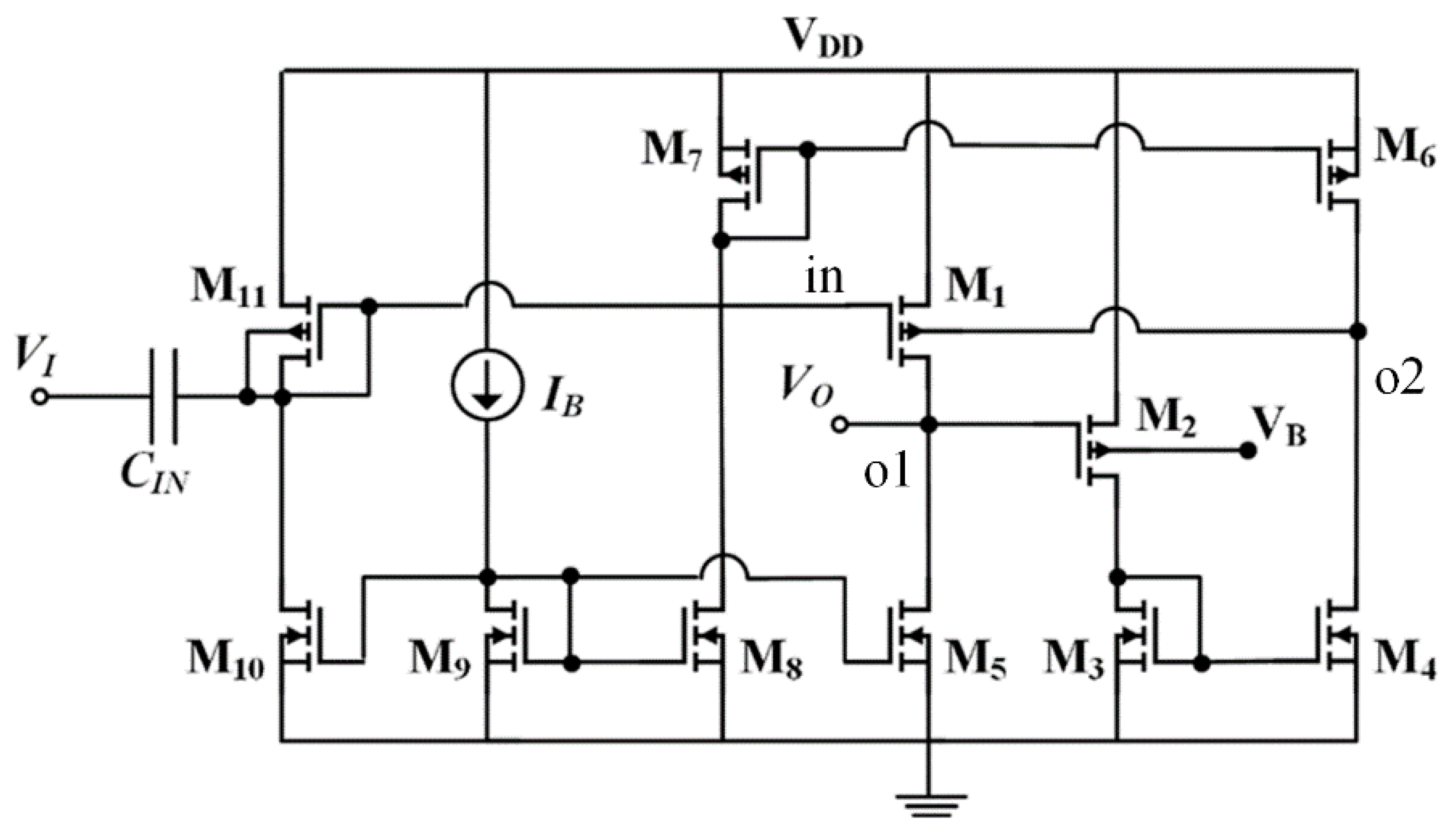
2.1. Circuit Description

Figure 1 shows the circuit schematic of the proposed band-pass filter. It is made up of common source transistor M1 implementing a first (inverting) gain stage biased by current generator M5. The input signal is AC coupled to the gate of M1 through capacitor CIN and the output of the filter is taken at the drain of M1 which drives also the second (noninverting) gain stage made up of common source transistor M2 and unitary current mirror M3–M4 biased by current generator M6. Transistors M7–M11 are used for biasing purposes. Negative feedback is accomplished by connecting the second stage output (drains of M4 and M6) to the bulk of M1. This loop also provides DC stabilization by setting the second stage output voltage to around VG11 thanks to the gate-bulk connection of M11 and circuit symmetry. The bulk of M2 is used for tuning the filter quality factor, Q, through voltage VB, as we will show in the followings.

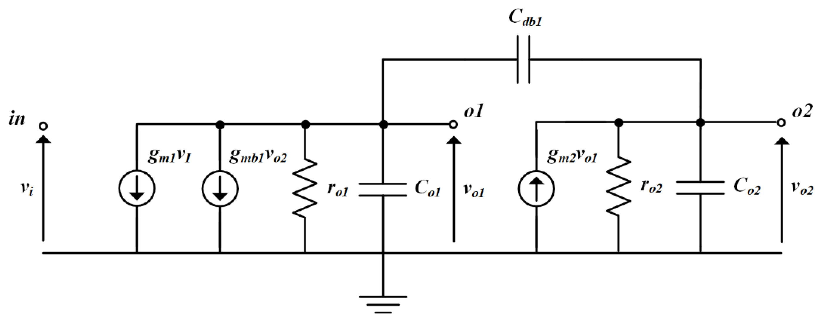
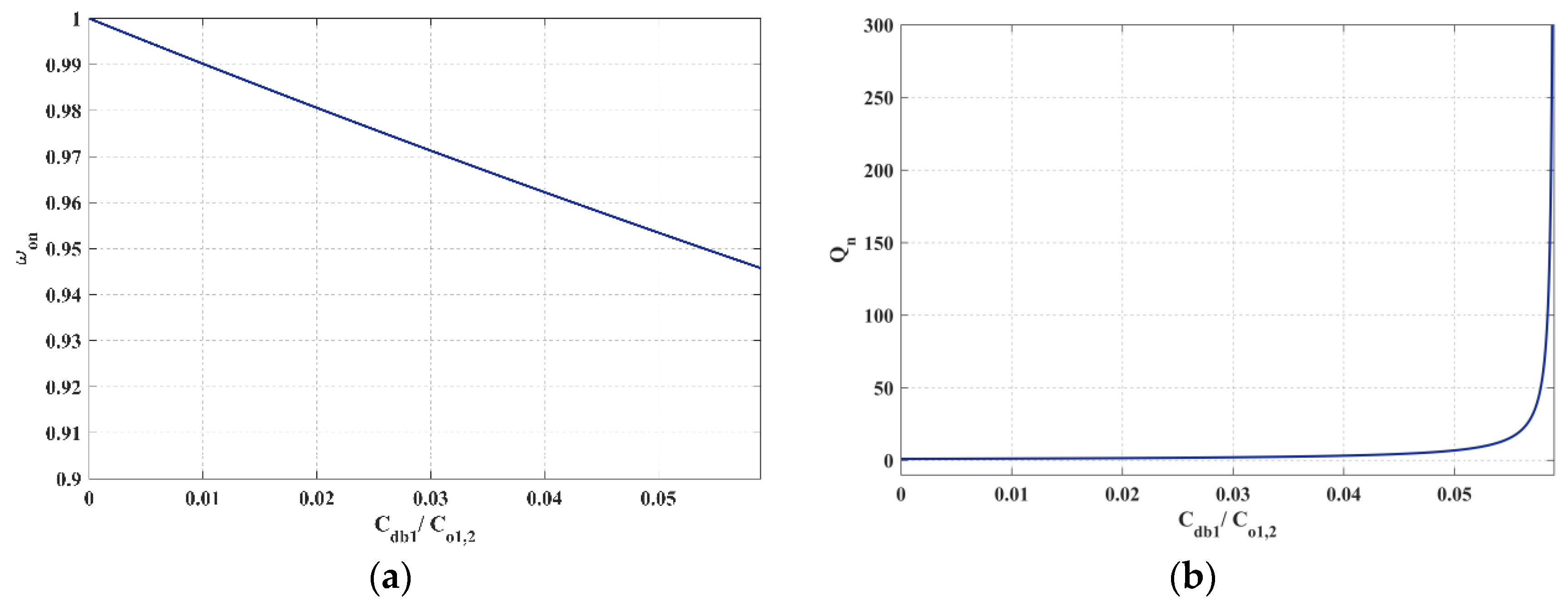
2.2. Circuit Analysis

Figure 2 illustrates the simplified small-signal equivalent circuit of the proposed solution, where gmi and gmbi are the gate-source and source-bulk transconductances of the i-th transistor. Cdb1 is the drain-bulk capacitance of M1 and ro1, ro2 and Co1, Co2 are, respectively, the equivalent resistances and capacitances at the nodes o1 and o2 (being o1 the filter output terminal. The expressions of these small signal parameters are given below
r o 1 = r d 1 r d 5
r o 2 = r d 4 r d 6
C o 1 = C g s 2 + ( 1 + g m 2 / g m 3 ) C g d 2 + C d b 5 + C g d 5 + C g d 1
C o 2 = C d b 4 + C d b 6 + C b s 1 + C g d 4 + C g d 6
We will show that Co1 and Co2 play an important role in setting the filter resonant frequency while Cdb1 is fundamental in the selection of Q. Observe that AC coupling capacitance CIN is neglected here, as its effect is well known; indeed, it introduces a zero at ω = 0 and a low-frequency pole p I N = g m 11 / C I N in the input-output transfer function.
After standard calculation and neglecting higher-order terms, the resulting transfer function Vo1/Vi is given by
H ( s ) = V o 1 V i g m 1 r o 1 1 + g m b 1 g m 2 r o 1 r o 2 1 + s r o 2 ( C o 2 + C d b 1 ) 1 + a 1 s + a 2 s 2
where
a 1 = C d b 1 [ r o 1 + r o 2 + ( g m b 1 g m 2 ) r o 1 r o 2 ] + r o 1 C o 1 + r o 2 C o 2 1 + g m b 1 g m 2 r o 1 r o 2
and
a 2 = r o 1 r o 2 [ C d b 1 ( C o 1 + C o 2 ) + C o 1 C o 2 ] 1 + g m b 1 g m 2 r o 1 r o 2
Assuming gmb1gm2ro1ro2 >> 1, the outband filter gain, Hob, is from (2)
H ob = g m 1 r o 1 1 + g m b 1 g m 2 r o 1 r o 2 g m 1 g m b 1 g m 2 r o 2
which becomes conveniently less than 1, provided that gmb1ro2 > gm1/gm2, a condition that is usually met.
Under the same assumption, gmb1gm2ro1ro2 >> 1, the resonant angular frequency, ωo, and quality factor are respectively given by
ω o = 1 a 2 g m b 1 g m 2 C d b 1 ( C o 1 + C o 2 ) + C o 1 C o 2
Q = a 2 a 1 g m b 1 g m 2 [ C o 1 C o 2 + C d b 1 ( C o 1 + C o 2 ) ] [ r o 1 + r o 2 + ( g m b 1 g m 2 ) r o 1 r o 2 ] C d b 1 + r o 1 C o 1 + r o 2 C o 2 r o 1 r o 2
The above expressions can be further simplified as a result of the straightforward design strategy that takes advantage of similar transistor dimensions and bias currents for the two common-source stages in order to gain further insight into the above equations useful during the design phase. In this case, we can set ro1 = ro2 = ro1,2 and, somehow, oversimplifying, Co1 Co2 = Co1,2, yielding
ω o g m b 1 g m 2 C o 1 , 2 1 1 + 2 C d b 1 / C o 1 , 2 g m b 1 g m 2 C o 1 , 2
Q g m b 1 g m 2 2 r o 1 , 2 1 + 2 C d b 1 / C o 1 , 2 1 + [ 1 + ( g m b 1 g m 2 ) r o 1 , 2 / 2 ] C d b 1 / C o 1 , 2 1 2 g m b 1 g m 2 r o 1 , 2 1 + [ 1 + ( g m b 1 g m 2 ) r o 1 , 2 / 2 ] C d b 1 / C o 1 , 2
The approximated expression in (6a) shows that ωo is determined by the ratio of the square root of gmb1gm2 to Co1,2, as Cdb1 is intrinsically lower than Co1,2 and, consequently, 2Cdb1/Co1,2 can be neglected with respect to the unity. This condition can be also ensured by adding parallel capacitances to Co1 and Co2 at the expense of a proportional reduction of ωo that, in this way, can be decreased by several decades, offering wide range of frequency application. Of course, CIN must be increased accordingly to set the input pole well below the resonant angular frequency. However, (6a) indicates that, to maximize ωo for a given transconductance level of gm2 and gmb1 (observe that gmb1 is a known fraction of gm1), the design effort should be aimed at minimizing Co1,2.
It is also to be noted that ωo can be finely and continuously tuned by varying the transconductances in (6a) by varying, in turn, the DC current IB in Figure 1. Once ωo is set, (6b) shows that also Q is set because both ωo and Q depend on the same parameters. It is seen that, due to the minus sign in the denominator of (6b), very high Q values can be achieved. Indeed, the term proportional to gmb1gm2 is negative and tends to reduce the denominator. However, because Q must be positive to preserve stability, the following condition (7) must be ensured. In other words, Q tends to be infinitely large and then becomes negative if the first member of (7) approaches the second member and overtakes it. Additionally, in this case, if it is required to fulfil (7), additional capacitances in parallel to Co1,2 may be added.
g m 2 g m b 1 < 2 1 + C o 1 , 2 / C d b 1 r o 1 , 2
Some of the above considerations can be gained with the aid of Figure 3a,b, which, respectively, depict the normalized resonant frequency, ωon, and normalized quality factor, Qn, defined in (8a) and (8b) versus Cdb1/Co1,2, and where gmb1, gm2, and ro1 were set to 1.4 μA/V, 19 μA/V, and 2 MΩ, respectively.
ω o n = ω o / ( g m b 1 g m 2 , 4 / C o 1 , 2 ) = 1 / 1 + 2 C d b 1 / C o 1 , 2
Q n = Q / g m b 1 g m 2 2 r o 1 , 2 1 + 2 C d b 1 / C o 1 , 2 1 + [ 1 + ( g m b 1 g m 2 ) r o 1 , 2 / 2 ] C d b 1 / C o 1 , 2
The light dependence of ωon on Cdb1/Co1,2 can be appreciated from Figure 3a, which shows a 5% decrease as a result of a change in Cdb1/Co1,2 from 0 to 0.06. In contrast, the strong dependence of Qn on Cdb1/Co1,2 is apparent from Figure 3b, which shows the expected asymptote given by (7) when its first member equals the second member.
Because the high Q values achievable lead to a high circuit sensitivity to process tolerances and temperature variations, additional circuitry must be added to control this parameter, the development of which is beyond the scopes of this paper. From (6b) or (8b), it is seen that a possible way to provide continuous Q tunability is via gm2, which, in turn, can be electrically varied through VB in Figure 1. Observe that changing gm2 has a limited impact onto ωo because gm2 >> gmb1, as will be shown in the next simulations section.

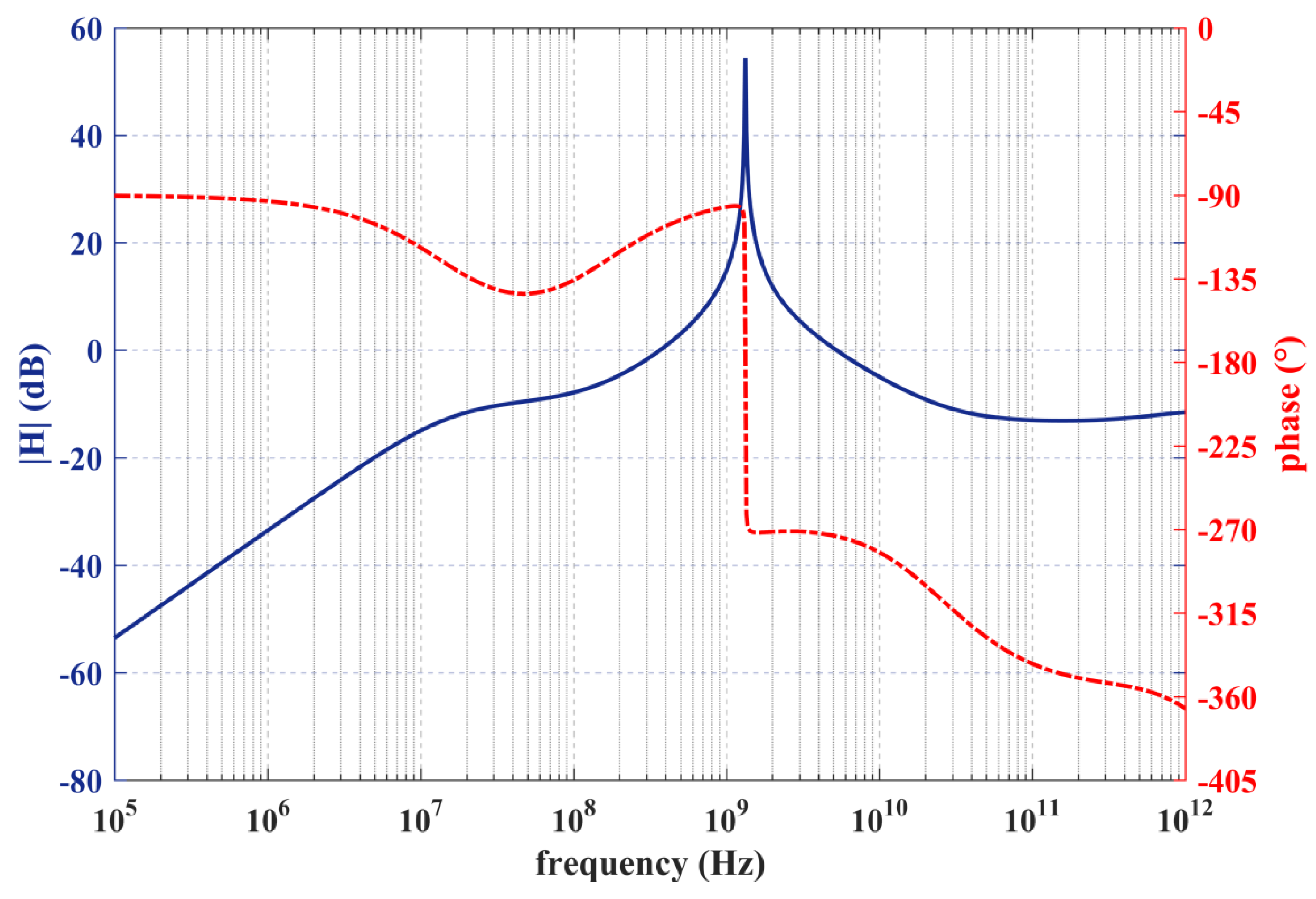
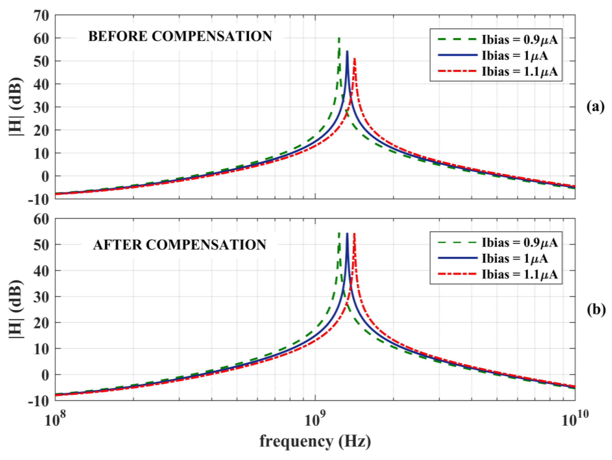
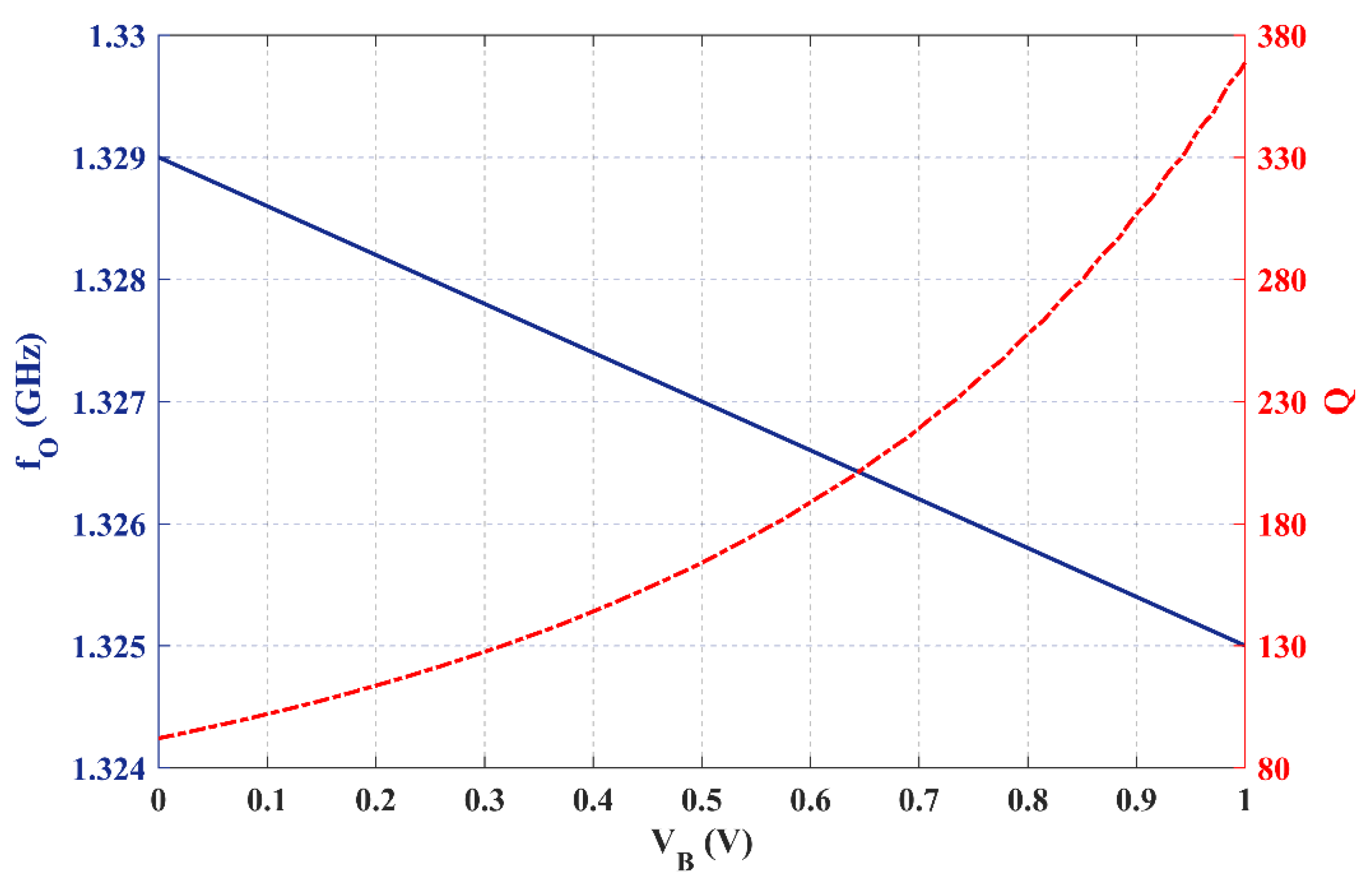
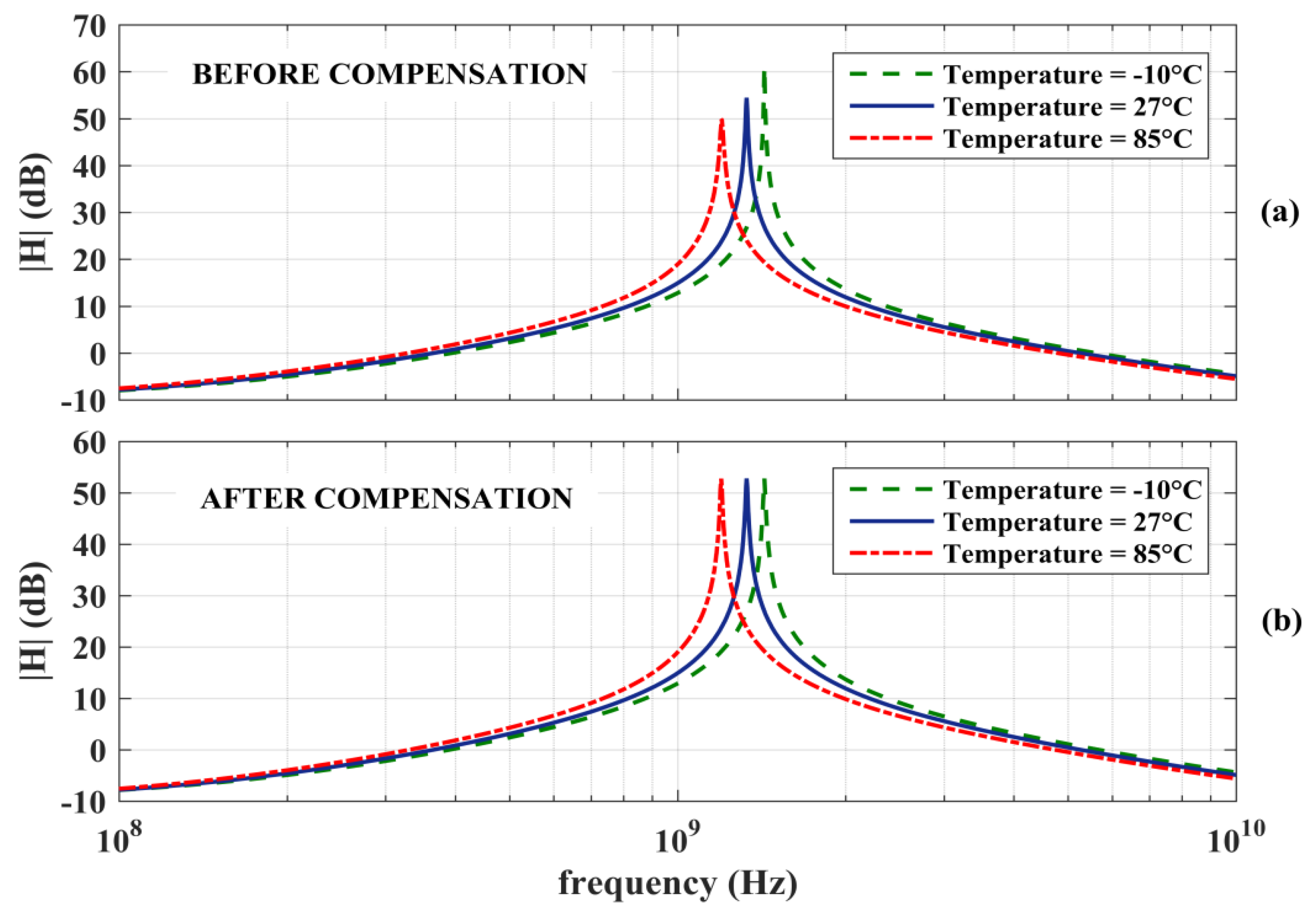
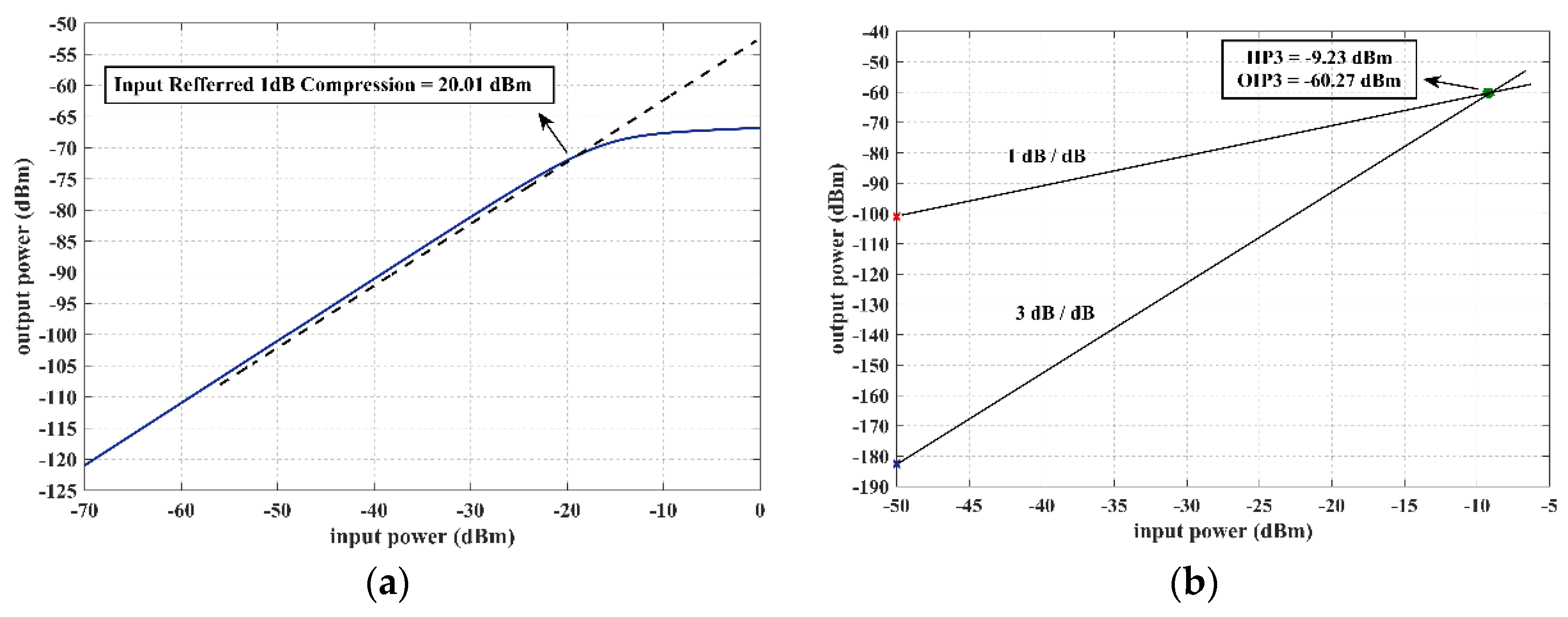
3. Validation Results

The proposed solution was designed in the 28-nm FDSOI technology provided by STMicroelectronics. Power supply was set to 1 V and transistor dimensions were set in order to achieve a resonant frequency of around 1 GHz with Q > 100, under a very limited current consumption of 6 μA (1 μA for each branch, including the reference one). The chosen design values and main small signal parameters are summarized in Table 1 and Table 2, respectively.
Using the values in Table 2 and the expressions that are found in Section 2.2, the low-frequency pole due to CIN results at around 14.4 MHz. The outband gain from (4) results to be 0.33 (−9.6 dB). The expected resonant frequency from (5a) is 1.46 GHz with expected quality factor from (5b) of 180. Note that the inaccurate estimation of Co1,2 may lead to strong errors, given the extreme sensitivity of this parameter. Figure 4 depicts the Bode plots (magnitude and phase) of the simulated circuit transfer function, which shows 2πωo = 1.33 GHz and Q = 164. The peak gain is 54.5 dB and the outband gain is −13 dB.
Figure 5a shows Bode plot magnitude for three different bias currents IB, namely 0.9 μA, 1 μA, and 1.1 μA. It is seen that the resonant frequency is shifted, respectively, from 1.24 GHz to 1.33 GHz and to 1.42 GHz. As an expected but unwanted effect of frequency tuning, the quality factor also changes from 312 to 164 and to 112. Equalization of the quality factors is possible through voltage VB, as explained in the previous section and illustrated in Figure 5b, where VB equal to 173 mV, 500 mV, and 904 mV is used to tune gm2 and achieve the same Q value of 164 in the three cases.
Figure 6 shows the plot of achieved resonant frequency and quality factor as a function of voltage VB in the nominal condition IB = 1 μA in order to better appreciate the Q tuning interval offered by the proposed design. It is seen that Q can be varied from around 90 to 370, while no appreciable change in the resonant frequency is produced.
The effect of temperature was simulated under three different conditions, namely −10 °C, 27 °C, and 85 °C. The obtained magnitude Bode plots are shown in Figure 7a. ωo/2π and Q are respectively 1.43 GHz and 353@−10 °C, 1.33 GHz and 164@27 °C, and 1.20 GHz and 95@85 °C. These limited variations are within the tuning range seen before and they can be counteracted by the use of concurrent IB and VB tuning. Figure 7b shows the result after Q tuning to the value of 164 by setting VB equal to 17 mV@−10 °C, 500 mV@27 °C, and 963 mV@85 °C.
Figure 8a,b show, respectively, the filter 1-dB compression point, P1dB, and third-order intercept point, IP3. The value of P1dB is −20.5 dBm and input-referred IP3 is −9.23 dBm. Noise Figure was 31 dB and spurious free dynamic range, SFDR, was 71.6 dBm.
Linearity was evaluated under −50 dB input power. The third-order intermodulation distortion, IMD3, was found to be −79 dBm and it was simulated by a two-tone test with 11 MHz spacing at 1.33 GHz, within the band of interest.
Table 3 shows the summary and comparison of this work with other second-order band pass filters in the literature. A figure-of-merit, FOM, is also used for overall performance comparison [20,21]
F O M = N P 1 d B , W f o Q P d c N F
where N is number of poles (filter order), P1dB,W is the in-band 1-dB compression point in watts, fo is the resonant frequency, Q is the quality factor, Pdc is dc power consumption in watts, and NF is the noise figure (not in decibels). Higher FOM mean better performance. The proposed solution exhibits the lowest power consumption and lowest supply voltage, with FOM being one of the highest.

4. Conclusions

Although the “fourth” MOS terminal has been used for decades in the digital domain and even in the analog one [17,18], the body-source biasing was limited to only around 300 mV in order to avoid junction turn on and, hence, restricting the designer options and/or compatible supply voltage. The advent of FD-SOI technologies has made possible the full exploitation of the body as an independent terminal available to the designer, so that new circuits schemes that use the bulk with much more flexibility and efficiency can be developed. In this paper, a new micropower bandpass filter topology that exploits the MOS bulk terminal in the dc stabilization loop and also as a means of quality factor tuning is proposed and preliminary simulations are presented to show its potential in terms of achievable operating frequencies and quality factors. No particular application or standard has been targeted. Lower filter resonant frequency can be achieved by adding two capacitors at nodes o1 and o2 in Figure 2, whereas higher resonant frequency can be achieved by increasing the standby current. The main advantage of the solution is its high frequency capability requiring only a few microamperes of current consumption. The main drawback is related to the dependence of ωo to the bulk transconductance, that is a fraction of the gate transconductance, thus limiting the maximum achievable ωo. Further investigation is currently carried out to avoid this drawback as well realize a higher-order filter function with automatic tuning control for specific applications.

Author Contributions

Conceptualization: S.P.; data curation: A.B.; original draft preparation: S.P. and A.B.; writing, review and editing: A.B., A.D.G., S.P., C.V.; formal analysis: A.D.G., A.B. and S.P.; supervision: A.D.G. and S.P. All authors have read and agreed to the published version of the manuscript.

Funding

This research received no external funding.

Conflicts of Interest

The authors declare no conflict of interest.

References

  1. Cathelin, A. Fully Depleted Silicon on Insulator Devices CMOS: The 28-nm Node Is the Perfect Technology for Analog, RF, mmW, and Mixed-Signal System-on-Chip Integration. IEEE Solid-State Circuits Mag. 2017, 9, 18–26. [Google Scholar] [CrossRef]
  2. Fridi, A.R.; Zhang, C.; Bellaouar, A.; Tran, M. A Low Power Fully-Integrated 76-81 GHz ADPLL for Automotive Radar Applications with 150 MHz/us FMCW Chirp Rate and -95dBc/Hz Phase Noise at 1 MHz Offset in FDSOI. In Proceedings of the 2019 IEEE Radio Frequency Integrated Circuits Symposium (RFIC), Boston, MA, USA, 2–4 June 2019; pp. 327–330. [Google Scholar]
  3. Couso, C.; Martin-Martinez, J.; Porti, M.; Nafría, M. Performance and Power Consumption Trade-Off in UTBB FDSOI Inverters Operated at NTV for IoT Applications. IEEE J. Electron Devices Soc. 2018, 6, 55–62. [Google Scholar] [CrossRef]
  4. Le, Q.H.; Huynh, D.K.; Wang, D.; Kämpfe, T.; Lehmann, S. DC-110 GHz Characterization of 22FDX® FDSOI Transistors for 5G Transmitter Front-End. In Proceedings of the ESSDERC 2019—49th European Solid-State Device Research Conference (ESSDERC), Cracow, Poland, 23–26 September 2019; pp. 218–221. [Google Scholar]
  5. Ayele, G.T.; Monfray, S.; Ecoffey, S.; Boeuf, F.; Cloarec, J.P.; Drouin, D.; Souifi, A. Ultrahigh-Sensitive CMOS pH Sensor Developed in the BEOL of Standard 28 nm UTBB FDSOI. IEEE J. Electron Devices Soc. 2018, 6, 1026–1032. [Google Scholar] [CrossRef]
  6. Kargaran, E.; Guo, B.; Manstretta, D.; Castello, R. A Sub-1-V, 350-μW, 6.5-dB Integrated NF Low-IF Receiver Front-End for IoT in 28-nm CMOS. IEEE Solid-State Circuits Lett. 2019, 2, 29–32. [Google Scholar] [CrossRef]
  7. Elsayed, O.; Zarate-Roldan, J.; Abuellil, A.; Hussien, F.A.; Eladawy, A.; Sánchez-Sinencio, E. Highly Linear Low-Power Wireless RF Receiver for WSN. IEEE Trans. VLSI Syst. 2019, 27, 1007–1016. [Google Scholar] [CrossRef]
  8. Abella, C.S.; Bonina, S.; Cucuccio, A.; D’Angelo, S.; Giustolisi, G.; Grasso, A.D.; Imbruglia, A.; Mauro, G.S.; Nastasi, G.A.; Palumbo, G.; et al. Autonomous Energy-Efficient Wireless Sensor Network Platform for Home/Office Automation. IEEE Sens. J. 2019, 19, 3501–3512. [Google Scholar] [CrossRef]
  9. Kim, B.; Lee, J.; Lee, J.; Jung, B.; Chappell, W.J. RF CMOS Integrated On-Chip Tunable Absorptive Bandstop Filter Using Q-Tunable Resonators. IEEE Trans. Electron Devices 2013, 60, 1730–1737. [Google Scholar] [CrossRef]
  10. Lee, M.; Wu, H.; Tzuang, C.K.C. 1.58-GHz Third-Order CMOS Active Bandpass Filter with Improved Passband Flatness. IEEE Trans. Microw. Theory Tech. 2011, 59, 2275–2284. [Google Scholar] [CrossRef]
  11. Wang, S.; Chang, R.H. 2.4 GHz CMOS bandpass filter using active transmission line. Electron. Lett. 2016, 52, 371–372. [Google Scholar] [CrossRef]
  12. Nguyen, H.; Kim, K.; Han, S.; Lee, J.; Kim, C.; Lee, S. A Low-Power Interference-Tolerance Wideband Receiver for 802.11af/ah Long-Range Wi-Fi with Post-LNA Active N-Path Filter. IEEE Trans. Microw. Theory Tech. 2018, 66, 2287–2298. [Google Scholar] [CrossRef]
  13. Amin, F.; Raman, S.; Koh, K. Integrated Synthetic Fourth-Order Q-Enhanced Bandpass Filter with High Dynamic Range, Tunable Frequency, and Fractional Bandwidth Control. IEEE J. Solid-State Circuits 2019, 54, 768–784. [Google Scholar] [CrossRef]
  14. Lechevallier, J.; Struiksma, R.; Sherry, H.; Cathelin, A.; Klumperink, E.; Nauta, B. 5.5 A forward-body-bias tuned 450MHz Gm-C 3rd-order low-pass filter in 28nm UTBB FD-SOI with >1dBVp IIP3 over a 0.7-to-1V supply. In Proceedings of the 2015 IEEE International Solid-State Circuits Conference—(ISSCC) Digest of Technical Papers, San Francisco, CA, USA, 22–26 February 2015; pp. 1–3. [Google Scholar]
  15. Wang, S.; Lin, W. C-band complementary metal-oxide-semiconductor bandpass filter using active capacitance circuit. IET Microw. Antennas Propag. 2014, 8, 1416–1422. [Google Scholar] [CrossRef]
  16. Zhang, Y.; Kinget, P.R.; Pun, K. A 0.032-mm² 43.3-fJ/Step 100-200-MHz IF 2-MHz Bandwidth Bandpass DSM Based on Passive N-Path Filters. IEEE J. Solid-State Circuits 2020. early access. [Google Scholar] [CrossRef]
  17. Monsurró, P.; Pennisi, S.; Scotti, G.; Trifiletti, A. Exploiting the Body of MOS Devices for High Performance Analog Design. IEEE Circuits Syst. Mag. 2011, 11, 8–23. [Google Scholar] [CrossRef]
  18. Ballo, A.; Grasso, A.D.; Pennisi, S. Active load with cross-coupled bulk for high-gain high-CMRR nanometer CMOS differential stages. Int. J. Circuit Theory Appl. 2019, 47, 1700–1704. [Google Scholar] [CrossRef]
  19. Cellucci, D.; Centurelli, F.; Di Stefano, V.; Monsurrò, P.; Pennisi, S.; Scotti, G.; Trifiletti, A. 0.6-V CMOS cascode OTA with complementary gate-driven gain-boosting and forward body bias. Int. J. Circuit Theory Appl. 2020, 48, 15–27. [Google Scholar] [CrossRef]
  20. Gao, Z.; Ma, J.; Yu, M.; Ye, Y. A fully integrated CMOS active bandpass filter for multiband RF front-ends. IEEE Trans. Circuits Syst. II Expr. Briefs 2008, 55, 718–722. [Google Scholar]
  21. Kumar, V.; Mehra, R.; Islam, A. A 2.5 GHz Low Power, High-Q, Reliable Design of Active Bandpass Filter. IEEE Trans. Device Mater. Reliab. 2017, 17, 229–244. [Google Scholar] [CrossRef]
  22. Dülger, F.; Sánchez-Sinencio, E.; Silva-Martínez, J. A 1.3-V 5-mW fully integrated tunable bandpass filter at 2.1 GHz in 0.35-µm CMOS. IEEE J. Solid-State Circuits 2003, 38, 918–928. [Google Scholar]
  23. Kuhn, W.B.; Nobbe, D.; Kelly, D.; Orsborn, A.W. Dynamic range performance of on-chip RF bandpass filter. IEEE Trans. Circuits Syst. II Analog Digit. Signal Process. 2003, 50, 685–694. [Google Scholar] [CrossRef] [Green Version]
  24. He, X.; Kuhn, W.B. A 2.5-GHz low-power, high dynamic range, self-tuned Q-enhanced LC filter in SOI. IEEE J. Solid-State Circuits 2005, 40, 1618–1628. [Google Scholar]
Figure 1. Schematic of the proposed solution.
Jlpea 10 00027 g001
Figure 2. Simplified small-signal equivalent of circuit in Figure 1, vo1 = vo is the filter output.
Jlpea 10 00027 g002
Figure 3. (a) Normalized resonant frequency defined in (8a) versus Cdb1/Co1,2 and (b) normalized quality factor defined in (8b) versus Cdb1/Co1,2.
Jlpea 10 00027 g003
Figure 4. Transistor level simulation of the filter frequency response with the nominal design values in Table 1. 2πωo = 1.33 GHz and Q = 164.
Jlpea 10 00027 g004
Figure 5. Magnitude of the filter transfer function versus frequency under three different bias currents: (a) without compensation (VB = 500 mV), 2πωo and Q are respectively 1.24 GHz and [email protected] μA, 1.33 GHz and 164@1 μA and 1.42 GHz and [email protected] μA; (b) the three curves display the same Q of 164 obtained by setting VB equal to 173 [email protected] μA, 500 mV@1 μA and 904 [email protected] μA.
Jlpea 10 00027 g005
Figure 6. Filter resonant frequency and quality factor versus voltage VB.
Jlpea 10 00027 g006
Figure 7. Filter frequency response (magnitude) under three different simulated temperatures: (a) without compensation (VB = 0.5 V) ωo/2π and Q are respectively 1.43 GHz and 353@−10 °C, 1.33 GHz and 164@27 °C and 1.20 GHz and 95@85 °C; (b) with compensation the three curves display the same Q of 164 obtained by setting VB equal to 17 mV@−10 °C, 500 mV@27 °C and 963 mV@85 °C.
Jlpea 10 00027 g007
Figure 8. (a) The filter 1-dB compression point curve and (b) third-order intercept point curves.
Jlpea 10 00027 g008
Table 1. Design parameters used in simulations.
ParameterValue [nm/nm]ParameterValue [nm/nm]
(W/L)1180/90(W/L)9360/90
(W/L)2315/90(W/L)10360/90
(W/L)3360/90(W/L)11180/90
(W/L)4360/90CIN200 fF
(W/L)5360/90VDD1 V
(W/L)6360/90IB1 μA
(W/L)7360/90VB0.5 V
(W/L)8360/90
Table 2. Small signal parameters.
ParameterValue
gm1 = gm1118.1 μA/V
gmb11.4 μA/V
gm218.9 μA/V
ro12.03 MΩ
ro22.01 MΩ
Co1640 aF
Co2450 aF
Cdb130 aF
CIN200 fF
Table 3. Comparison with the state of the art.
This Work a[22][23][24][20][21] a
Technology28 nm FDSOI0.35 μm0.5 μm0.5 μm SOI0.18 μm45 nm
Filter order222222
Resonant freq. (GHz)1.332.190.92.52.442.511
Quality factor1644345366069
Supply voltage (V)11.2331.8±1
Power (mW)0.0065.2391510.80.168
Noise figure (dB)3126.82161829.62
P1dB (dBm)−20.5−30−5.5−15−15−1.5
FOM (dB)874967807192
a Simulation results.

