A Review of the Characteristics, Synthesis, and Thermodynamics of Type-II Weyl Semimetal WTe2


School of Electro-Mechanical Engineering, Xidian University, Number 2 Taibai South Road, Xi’an 710071, China
*
Author to whom correspondence should be addressed.
Materials 2018, 11(7), 1185; https://0-doi-org.brum.beds.ac.uk/10.3390/ma11071185
Submission received: 4 June 2018
/
Revised: 6 July 2018
/
Accepted: 6 July 2018
/
Published: 10 July 2018
Abstract
:WTe2 as a candidate of transition metal dichalcogenides (TMDs) exhibits many excellent properties, such as non-saturable large magnetoresistance (MR). Firstly, the crystal structure and characteristics of WTe2 are introduced, followed by a summary of the synthesis methods. Its thermodynamic properties are highlighted due to the insufficient research. Finally, a comprehensive analysis and discussion are introduced to interpret the advantages, challenges, and future prospects. Some results are shown as follows. (1) The chiral anomaly, pressure-induced conductivity, and non-saturable large MR are all unique properties of WTe2 that attract wide attention, but it is also a promising thermoelectric material that holds anisotropic ultra-low thermal conductivity (0.46 W·m−1·K−1). WTe2 is expected to have the lowest thermal conductivity, owing to the heavy atom mass and low Debye temperature. (2) The synthesis methods influence the properties significantly. Although large-scale few-layer WTe2 in high quality can be obtained by many methods, the preparation has not yet been industrialized, which limits its applications. (3) The thermodynamic properties of WTe2 are influenced by temperature, scale, and lattice orientations. However, the in-plane anisotropy cannot be observed in the experiment, as the intrinsic property is suppressed by defects and boundary scattering. Overall, this work provides an opportunity to develop the applications of WTe2.
1. Introduction
Weyl semimetal (WSM) is a new state of matter in condensed matter physics that contains Weyl fermions acting as emergent quasiparticles. Its bulk material owns the Fermi arc surface state at the boundary, and this novel electronic structure makes it hold characteristics of topological properties. In 2016, many researchers reported that the Fermi arcs on its surface, and that Fermi cones and Weyl nodes in the bulk of WSM could be observed through photoelectron spectroscopy directly [1,2,3,4]. Also, WSM is a new generation of topological insulators with unique band structures on the surface and in the bulk, which means that it is different from the topological insulators that are characteristic of gapless surface states protected by time-reversal symmetry. In addition, the robust topological states at the step edge of WTe2 can be directly observed by spectroscopic-imaging scanning tunneling microscopy (STM) in the experiment, which validates the prediction by first principle theory [5]. The WSM phase stands between the general phase and the topological phase, and the effective band is a low-energy linear Dirac-type dispersion. The Weyl fermions in the bulk can be utilized to study the chiral anomaly in the condensed matter physics field; meanwhile, it owns huge unsaturated magnetoresistance (MR), which makes it a promising type of material. Since the discovery of non-magnetic WSM including TaAs, TaP, NbAs, and NbP by Weng et al. in 2015, it has found that they are unique from the traditional magnetic WSM in terms of electromagnetism [6]. The type-I WSM, such as TaAs, produces a large non-saturated negative MR in parallel electric and magnetic fields, whereas type-II WSM such as WTe2 possesses a positive MR that is related to crystal orientations. It should be noted that spatial inversion symmetry cannot be observed in TaAs, and the position of the k-space of the Fermi arc terminal on the surface matches the projection of numerous Weyl nodes on the surface Brillouin zone. Furthermore, the Fermi arc on the surface of WSM contributes to the quantum oscillations of magnetic transport. As a result, its excellent electromagnetic property also attracts many researchers, but meanwhile, WSM is also a promising thermoelectric material. Specifically, it holds a high thermoelectric figure of merit and low thermal conductivity, so it is potentially used in thermoelectric fields. However, there are few studies in this field.
WTe2 as a non-magnetic thermoelectric semimetal is a recently discovered type-II WSM. It has become a research hotspot owing to its huge non-saturated MR and chiral anomaly. Except for graphene, the limitations of other two-dimensional (2D) atomic-level thickness metals such as β-MoTe2 and WTe2 are studied insufficiently. They are stable as semimetals in the deformation of the octahedral 1T (CdI2) geometry, possessing an in-plane bending chain formed by Mo/W atom pairs dimerized in charge exchange between metals, and Van der Waals forces play a role in the bonding interactions among dominant layers [7]. MoTe2 can be synthesized in 2H and 1T polytypes or reversibly converted between the two polytypes as a function of temperature or strain. Since the 1960s, WTe2 has been proven that it has an orthogonal structure with a space group Pmn21 (Td), and it is one of the most promising dichalcogenides in the VI groups. The 2D transition metal dichalcogenides (TMD) materials (AB2: A is W or Mo; B is S, Se or Te) can be used in applications of low-dissipation electronics, spintronics, optoelectronics, and catalysis. Recently, it is also well known due to many excellent properties including unsaturated MR along the a-axis, superconductivity induced by pressure, spin-orbit structure, temperature-driven Lifshitz transition, and low-energy light absorption [8]. The spin-orbit out-of-plane field-like torque is related to the thickness significantly, but the magnitude of the out-of-plane antidamping torque is weakly influenced by thickness [9]. In addition, a novel Weyl fermion is observed in WTe2 firstly that is different from conventional one, and the monolayer material has a quantum spin Hall effect. However, in addition to electro-optical properties, the thermal properties are also critical, because it determines the heat dissipation efficiency, which is a significant parameter for the performance and reliability of devices.
The WSM is a new generation of topological semimetal materials developed from topological insulators, and its research is still in its infancy. Many of its researches are based on its electromagnetic properties, and there are few studies on its thermodynamic properties. The WTe2 is one of the most valuable materials in the thermodynamic field, so this paper summarizes its main features, and the researches of thermodynamics are mainly summarized and analyzed as a supplement of studies, which is helpful for the development of this new material.
2. Structure and Characteristics of WTe2
2.1. Crystal Structure and Surface Structure
WTe2 is a typical candidate of layered TMDs [10]. Its distorted 1T (Td) structure can be observed by atomic resolution imaging in the bulk material at 300 K, which is different from most TMDs (2H or 1T) [11]. Figure 1 shows the layered crystal structure of WTe2 and its Brillouin zone [12]. Its crystal structure can be regarded as the distortion of MoS2 along the a-axis (W chain). It is similar to graphite to some extent in that it is composed of many layers, and the W layers are separated from each other by two layers of Te, which is stacked along the z-axis. The number of layers can be observed by the Raman modes in Raman spectroscopy [13]. The lattice structure is orthorhombic, and the space group is Pmn21 (C72v). The distance between adjacent W atoms is smaller along the x-axis than that along the y-axis or the z-axis, which results in strong anisotropy. The topological surface state exists because all of the Weyl points (WPs) are projected onto different points for the (001) surface.
WTe2 and β-MoTe2 are typical semimetals because the displacement of W and Mo atoms from the octahedron center of Te atoms compensates for the loss of band structure. Actually, the crystal structure of Td-WTe2 is similar to that of β-MoTe2. The coordination of a distorted octahedron of Te atoms around the W atoms displaces them from the octahedron center in the ab-plane, but the layered configuration still exists along the c-axis, as shown in Figure 1c. This distorted structure contributes to a rise of the coordination number (from six to eight) for the tungsten. However, their stacking layers are different from that of an orthorhombic symmetry and a monoclinic symmetry, which are shown in WTe2 (Pmn21) and β-MoTe2 (P21/m), respectively [14]. Furthermore, 2H and 1T are common crystal structures for TMDs such as MoTe2. A trigonal prismatic coordination (six chalcogen atoms) is around the Mo atoms, and a slight elongation of the prism is shown vertically to the layers, which represents the 2H-polytype of MoTe2. In addition, the 2H structure consists of three hexagonal atoms planes (chalcogen-metal-chalcogen) with a van der Waals force between layers along the c-axis, and strong covalent bonds connect the in-plane atoms. The Madelung energy of Td-WTe2 is lower than that of assumed 2H-WTe2, which is the reason for the semimetal state [15]. Another typical structure of TMDs is 1T octahedral coordination, which is different from 2H in that the chalcogen atoms are located directly above each other in the trigonal prism. The W atoms are octahedrally coordinated by Te atoms for the 1T structure, but the sandwich layers are inverse for distorted 1T (Td). The displacement of the W atoms (horizontally by 0.95 Å toward the top Te chain and perpendicularly by 0.21 Å vis a vis the bottom W atom) from the octahedral center is related to the strong intermetallic bonding so that pairs can form, and a zig-zag pattern is also shown in crystal [16].
It is widely known that dichalcogenides such as WTe2 are suitable for the applications in environments with extreme temperatures and pressures in engineering, and they also can be employed in semiconductors, batteries, catalysts, etc. The dichalcogenides typically perform a layered structure of the compound in which a metal atomic layer is sandwiched between two chalcogen atoms, as shown in Figure 1a. Also, the chemical bonds of the atoms are relatively stable in the in-plane layer, while the interaction between out-of-plane layers is weak, owing to the connection of the van der Waals force. Therefore, the cracking tends to occur in this structure, and considerable anisotropy is shown in many physical properties. In addition, the distance between layers is wide enough to be doped by impurities, so the WTe2 is easy to be influenced by doping. A twisted octahedral coordination around tungsten atoms is performed in the structure that is in line with the morphology of the form of MoTe2 under high temperature. Its structure is different from most TMDs, which are characterized by the triangular prism or monoclinic structure. Furthermore, it is obvious from Figure 1a that the layers are curved, resulting from the dislocation of W atoms from the center of the octahedron, which forms a chain extending through the crystal. It is worth mentioning that the displacement of the W atom enhances the strength of metallic bond so that the conduction of WTe2 is improved, and it also contributes to a novel electronic band structure, which is the reason why WTe2 has a relatively high conductivity in dichalcogenides. It should be noted that some properties of the type-I and type-II WSMs are very different, such as the thermodynamic properties.
The surface structure of WTe2 is also important, and it is significantly associated with the unique features, such as the emergence of MR. The tellurium and tungsten layers are buckled in the direction of the c-axis, but the tellurium and tungsten atoms do not sit in the identical plane in every layer. In 1994, Crossley et al. studied the surface of WTe2 with [001] orientation in ultra-high vacuum by scanning tunneling spectroscopy (STS), and found that it depended on the polarity of tunnel voltage [16]. The tip effect might cause artefacts, which explained the STM images. In 1996, Hla et al. investigated the positions of atoms on the (001) surface of TMDs by varying the metal–Te distances [17]. The STM images in Figure 2a,b show the detailed corrugated Te atoms on the top and metal layers, and the results were compared with those by atomic force microscopy (AFM) in Figure 2c. They stated that only the Te-layer-like images were observed when the tip was far from the surface, and the results were not associated with the polarity of bias voltage, which was not in line with the theoretical results (observation was available only at the negative bias). In 2017, the atomic structure of the WTe2 surface was studied by Kawahara et al. by means of low-energy electron diffraction (LEED), STM, and density functional theory (DFT) [18]. In the first layer, a tiny surface relaxation was found, and it decayed in an oscillatory mode. In addition, they suggested that the topology of the Fermi surface was affected by the relaxation.
2.2. Classification
WSM is mainly divided into two types in accordance with fermions: type-I (TaAs, TaP, NbAs, and NbP) and type-II (WTe2 and MoTe2). Standard WPs exists on the spotted Fermi surface of Type-I WSM. By contrast, the type-II WPs are still the protected intersections, but occur at the boundary between the electron and hole pockets [12]. This is the reason why many properties are different for these two types of WSMs, and type-II WSM holds some novel physical phenomena as well, such as the open Fermi arcs existing on the Fermi surface, and planar orientation-dependent chiral anomaly [10,12].
2.3. Novel Weyl Fermions, Fermi Arcs, and Surface State
The fermion is a fundamental component in the atom, and is divided into three types as basic particles: Dirac, Majorana, and Weyl [12]. However, Majorana and Weyl fermions can only be observed in the state of low-energy excitation, so they are rarely observed in the experiments, but the discovery of topological superconductors and semimetals allows the observation of them in the experiments. Weyl fermions in the boundaries of hole pockets and electrons have been ignored because of the contravention of Lorentz symmetry in high-energy physics. By contrast, this theory is not included in condensed matter physics, and new Weyl fermions can be found by promoting Dirac equations. In monolayer WTe2, the special electron–hole-pocket structure cannot be observed due to the absence of interlayer interactions [19]. However, it can be modified by the transition-metal Ni-adsorbed system in accordance with density functional theory. Figure 3 shows the positions of the Fermi level and WP on the (001) surface [12]. The green line is the location of the Fermi level that is between the WPs, as shown in Figure 3a. In addition, the two crosses represent the WPs in Figure 3b, and it also shows a Fermi arc that connects the hole and electron pocket on the Fermi surface.
WTe2 owns a complex band structure and unique hole Fermi pockets, and this special electronic structure contributes to many novel characteristics, such as large MR. In Figure 4, two bands (green and blue) of the WSM cross at the Fermi level linearly, while the number of bands doubles for Dirac semimetal (DSM) [12]. Figure 4a illustrates the WP and punctate Fermi level of type-I WSM, while the WP exists at the boundaries between electron and hole pockets (blue/red lines) for type-II WSM, as shown in Figure 4b. The Fermi level is marked as grey flat, clearly. Also, the Weyl or the gapless Dirac equation can be used to describe respective Hamiltonian intersections. An interesting thing is that WPs generally appear in pairs, and the reason for this is that the net charge cannot exist throughout the Brillouin zone [20]. In addition, they cannot be affected by slight perturbations, and the electron pocket shows opposite behavior [21]. There are totally four pairs of WPs that are located between the Fermi levels of 0.052 eV and 0.058 eV. Furthermore, the Fermi arc is on the Fermi surface, and the cone-shaped spectrum is tilted due to dynamics, which does not follow the Lorentz invariance of the Weyl fermions in the quantum field. This special case was neglected before the discovery of WSM, but it proved the correctness of the existence of type-II WSM. Moreover, the tilted spectrum is associated with the dynamics in the spectrum as mentioned, specifically, the dynamics dominate in the exact direction in reciprocal space (potential component accounts for a small part). Then, the tilt is large enough for WP to appear at the boundary of electron and hole pockets, which is inverse to the case of type-I WSM (the particular direction cannot be found). Another difference is that type-II WSM does not show chiral anomaly under magnetic field in any directions, and this phenomenon can be observed only in which the magnetic field direction is in the cone.
In recent years, the electronic structures of WTe2, including WPs, trivial and nontrivial surface states, and Fermi arcs have been studied intensively by angle-resolved photoemission spectroscopies (ARPES) and STM/STS. The electronic structures of the top and bottom (001) surfaces are different. In 2016, Bruno et al. reported a surface state in which the Fermi arc emerged out of the bulk electron pocket on the top and bottom surfaces by small-spot laser ARPES [22]. They also stated that the Fermi arc was trivial in topology, and it was not related to the WPs in the bulk band structure, which indicated that it was impossible to observe the Fermi arc solely regarding the WTe2 as a WSM in topology. Furthermore, Sánchez-Barriga et al. used ultra-high-resolution ARPES to observe the Fermi arc on the (001) surface at 0.8 K in 2016 [23]. They believed that the Fermi arc was associated with the coupling to the surface resonance dispersing near the boundary of the projected band gap in bulk. They also suggested that it was trivial in topology by comparing the results in experiments and theoretical calculations, but the coupling showed compatibility with the type-II WSM possessing a topological Fermi arc.
In 2016, Wu et al. also investigated the electronic structure of WTe2 by ARPES, and confirmed the existence of Fermi arcs that linked the bulk electron and hole pockets on the (001) surface [3]. The WPs were observed at the boundary of the electron and hole pocket, as shown in Figure 4. Also, both trivial and topological areas existed on the same sample surface owing to uneven strain, which proved that the transition from a topological state to a trivial state could be driven by strain. In the same year, Feng et al. also observed and validated the prediction of spin polarization of both the Fermi arc and pockets by spin- and angle-resolved photoemission spectroscopy (SARPES) and theoretical calculations [24]. However, the location of WPs and the Fermi arc were not easy to identify by ARPES, because they stood above the Fermi level. To solve this problem, Lin et al. measured energy-dependent quasiparticle interference patterns by cryogenic STM, and identified that the location of WPs was (kx’, ky’, E) = (0.23 ± 0.01 Å−1, 0.05 ± 0.01 Å−1, 50 meV) [25]. The results had good agreement with the theoretical calculations, which proved that WTe2 was a type-II WSM. It should be noted that some contrary results about the topological nature of the Fermi arc still exist using ARPES. In 2017, Zhang et al. measured and interpreted the quasiparticle interference pattern of the surface state by STM and first-principles calculations, which confirmed the scattering of surface state [26]. However, they did not validate the existence of WPs in the bulk due to the spin-splitting effect, despite the observation of Fermi arcs.
2.4. Chiral Anomaly and Non-Saturable Large MR
The chiral anomaly and non-saturable large MR of WTe2 are related to its crystal structure. In Figure 1c, the a-axis (tungsten chain is marked by yellow lines) and b-axis are the two main axes in the crystal structure of WTe2 that are mutually perpendicular. A tungsten chain is along the a-axis in the crystal structure [10]. This special Td phase abolishes the inversion symmetry, which is the basis for supporting the existence of Type-II WP, and the interactions of electrons–holes contribute to planar orientation dependence, owing to the inclined band structure. Also, the non-saturable negative MR is observed along the a-axis when the electric field is parallel to the magnetic field, and the current is also perpendicular to the a-axis. Inversely, the positive MR emerges when the unsaturated electric field and the magnetic field are mutually vertical, and the current is parallel to the W-chain [10,27]. This unique phenomenon is associated with the chirality anomalies and plane orientation dependence of WTe2. Another reason why the MR is significantly large is that the electrical resistance rises significantly when the direction of the magnetic field is in line with the c-axis, which is absent in the type-I WSM. Furthermore, the flakes should be thicker to suppress the positive MR for the sake of observing this phenomenon. Alternatively, it can also be suppressed by rising pressure, and it can even be eliminated under pressure of 10.5 Pa, which is defined as the critical pressure or transformation pressure [28]. The lattice constant c is decreased during the pressurizing process, but the phase change of the structure is not observed. However, the quantum phase change happens when the pressure is over the critical pressure. According to the research by Krishna and Maitra in 2018, the magnetic field could improve the dimension of hole pockets in the Γ–Z direction, so the topology of the Fermi surface was influenced as well [29]. The MR was suppressed dramatically for the layered WTe2 flakes, owing to the decrease of the mobility of electrons and holes [30]. This was also related to the disorder and the amorphous surface oxide layer. Actually, the MR is influenced by doping such as Ga+ [31]. The presence of impurities can reduce the concentrations of electrons and holes, thereby changing the band structure and Fermi surface of WTe2. Also, the linear MR can be recognized by creating the mobility spectra for weak magnetic fields, and it dominates in a strong field (20 T) [32]. The large MR can be switched on and off by electrostatically doping between a semimetal state and metallic state (only electron) at low temperatures [33].
Research by Ali et al. in 2014 demonstrated that the MR reached 4.527 × 10⁵% at 4.5 K and 1.3 × 10⁷% at 0.53 K and 60 T [34]. As a non-magnetic material, its large MR is different from that of magnetic materials because of the reasonable compensation and equilibrium between the electrons and holes on the Fermi surface below 150 K in the Brillouin zone in the direction of Γ–X. In addition, the balance between the holes and electron carriers also makes the MR sensitive to the pressure, because the pressure tends to influence the lattice structure and balanced state of WTe2 [35]. The real carrier concentration can be determined with a large Seebeck coefficient without doping in the heterojunction structure [36]. However, it should be noted that the layered WTe2 is not available naturally, and the precursor purifying it is difficult to carry out during the preparation. It also tends to be degraded or oxidized when it is exposed in air, which all increase the difficulty of studying layered dependence properties. By contrast, the MR of WTe2 may be improved by up to 30% by the oxidization of the surface in accordance with the research by Li et al. [37].
The sheet-shaped and bulk material should have similar band structures so that WP can exist, and this is attributed to the reverse chirality of coupled WPs. Specifically, a non-zero potential is induced by electrons displacement if the dot product of the magnetic field and the electric field is not zero. The Fermi energy is influenced by the WP that can be controlled by the gate voltage; therefore, the transmission performance is also affected, which expands the applications of WTe2 in electronics. In addition, it also has potential as a two-dimensional (2D) contact material due to its relatively low work function.
2.5. Metal–Insulator Transitions
In 2015, Wang et al. discovered that the conductivity of layered WTe2 was associated with its thickness: the conductive resistivity started to transform to the insulated resistivity when the thickness of WTe2 was below six layers because of oxidation-induced disorders [38]. The dimension of layered WTe2 is not proportional to the number of layers due to the atomic force between layers (i.e., 7.9–8.6 nm for 11 layers) [7]. Also, the degradation or oxidation tends to influence the performance of WTe2-based devices, which is especially obvious in the case of fewer layers (i.e., less than four layers). The reason for this is that fewer layers result in a relatively unstable state, so oxidation between layers is severe when the thin WTe2 is exposed in the environment during manufacturing, such as during the exfoliation process [38]. As shown in Figure 5, the transport mode of WTe2 changes under approximately four layers, and the insulating property dominates when the number of layers is reduced to the limit of the monolayer (each layer owns a conductivity of ~e2/h). This is the proof of the metal-insulator transition of conductivity under the temperature dependence [38]. The conductivity is also related to the insulating temperature, especially for the tri and bilayers. It is worth mentioning that the conductivity of the monolayer is significantly low, which is neglected in Figure 5. The above experiment was carried out under low temperature, and the resistivity does not rise considerably under room temperature (i.e., increases five-fold at normal temperature compared to five to six orders of magnitude at T-0.25 K) [38].
The resistivity does not show the layer dependence significantly in the layer range studied. The reason for this may be that the curved W chain interrupts the in-plane 2D symmetry, which is characterized by preferred orientations, so different crystal orientations are performed in the device [7]. The rising interlaminar coupling of lattice distortion causes a moderately anisotropic Fermi surface in the planar layer.
2.6. Superconductivity
The superconductivity of WTe2 can be induced by increasing the pressure to 10.5 GPa at 2.8 K without changing the phase of the structure, and the large positive MR also disappears with the reversal of the sign of the Hall coefficient at this critical pressure [28]. The increasing pressure increases the number of electron carriers, but decreases the amount of hole carries, and the Fermi surface reconstructs with the change of quantum phase. Actually, the rebuilding of the Fermi surface depends on the anisotropy of lattice, and the a-axis, b-axis, and c-axis are compressed by 0.6%, 3.3% and 6.5% respectively. An interesting thing is that the anisotropy of superconductivity becomes very weak at 98.5 kpa by changing the magnetic field angle [39]. The critical temperature of superconductivity can also be enhanced by in-plane magnetic fields, although it may suppress the superconductivity because of the competition between thermodynamic and magnetic energies [40]. Also, complicated chemical doping can be avoided by controlling the pressure. It should be noted that the transition temperature of superconductivity decreases slightly with increasing pressure (i.e., from 6.5 K-13 GPa to 2.6 K-24 GPa). Furthermore, the pressure variation can also induce the phase change of single crystalline WTe2 [41]. The phase changes from orthorhombic Td to monoclinic T′ at 8 GPa because of inverse symmetry, which is in line with the observation of superconductivity.
3. Preparation of WTe2
Many methods are used to obtain WTe2 in different scales and shapes. These methods influence the properties of materials significantly, so they should be investigated to evaluate the availability. Mechanical exfoliation is the most basic method to obtain few-layer to single-layer WTe2 in high quality, and it is also applicable for other 2D layered materials such as graphene. However, this method is mainly utilized when large-scale WTe2 cannot be obtained, and WTe2 tends to degrade upon being exposed in air, so exfoliated flakes are limited to some extent. Other synthesis methods can also be used in real life, which promotes the development of WTe2-based devices and research.
3.1. Solid-State Reaction
The solid-state reaction can be used to manufacture single crystals of WTe2, and the pure powder of W is reacted with the excessive pure powder of Te in the environment of inert gases (i.e., argon) to improve the quality of WTe2 [28]. The mixture can be stored in the vacuum quartz container. In addition, the heating temperature is about 1273.15 K, and the mixture should be maintained for 5 h; then, it is cooled down to a lower temperature (973.15 K). In this process, the temperature gradient is very important, and should be controlled properly. The reacted WTe2 is finally centrifuged to get the single crystal compound.
3.2. Atmospheric Chemical Vapor Reaction
The WTe2 samples used in the most experiments are bulk material and flakes fabricated by mechanical exfoliation, because single layer WTe2 in good quality can be obtained. However, it is not practical in real applications due to the small-scale limit. In 2017, Zhou et al. firstly fabricated thin-film WTe2 by atmospheric chemical vapor reaction directly, and overcame the limitations of low Gibbs free energy (−26.2 kJ·mol−1) and the unmatched melting temperature of Te and W [42]. The synthesized polycrystalline WTe2 was in high quality, and held low thermal conductivity at 300 K (in plane: 2 W·m−1·K−1; though plane: 0.8 W·m−1·K−1), which was significantly lower than single crystalline flakes fabricated by mechanical exfoliation. In 2017, Chen et al. used ambient pressure chemical vapor deposition to synthesize large-scale layered 1T′-WTe2 (length of 350 µm) in good quality, and the nanooptical image technique was firstly applied to the WTe2 flakes for which the wavelength was obtained (100 nm) [43].
3.3. Chemical Vapor Deposition (CVD)
Chemical vapor deposition (CVD) is a common method that is used to synthesize layered 2D material such as graphene, and small-scale (even atomic scale) WTe2 film can also be obtained by this method [27]. In 2018, Li et al. synthesized uniform centimeter-scale (1 × 0.8 cm2), large-area WTe2 film in a few layers by CVD at low temperature, as shown in Figure 6, and the material was very stable at room temperature for one month despite a conductivity drop [37]. Figure 6b shows the thickness (6.02 nm) of synthesized 1T′-WTe2 by means of AFM, and it can be changed by regulating the sources (WCl6 powder is selected due to the lower melting point), amount, reacting time, and the reacting distance between WCl6 powder and the SiO2/Si substrate. The temperature used in this process was relatively low, which was only 500 °C, and the reaction lasted for 20 min at this temperature in the common three-zone system under the protection of N2/H2. Furthermore, Naylor et al. presented an accessible CVD method to fabricate monolayer 1T’-WTe2 flakes, and the surface coverage of this method was around 20%. They also suggested that the degradation of WTe2 could be averted by reducing the handling time and introducing few-layer graphene onto the substrate instantly after the reaction to passivate the WTe2 [44]. There are two stacking sequences in the bilayer WTe2, and low-temperature transport measurements indicate a semimetal–insulator transition, as mentioned [45].
3.4. Solution Synthesis
The few-layer Td-WTe2 nanostructure (30–50 nm) can be directly synthesized by the solution method at a relatively low temperature (300 °C), and the different growing paths show the multiple stacking motifs [46]. The advantage of this method is that the crystal structure can be adjusted by changing the amount of metal reagent. During the process, the temperature should be controlled properly to improve the purity of material. In 2018, Giri et al. obtained large-area atomically thin WTe2 by solution phase preparation [47]. A new Te precursor was also used to change the number of atomic layers (single to few layers).
3.5. Other Synthesis Methods
The eutectic metal alloy is a new method for the preparation of single crystalline WTe2, which can overcome the high vapor pressure of Te and low binding energy of W-Te [48]. The synthesis parameters of eutectic metal alloys can be studied to improve the quality of the material. The advantage of this method is that the WTe2 can be simply transferred to various substrates without degradation. Also, the single crystalline WTe2 (band gap is 1.44 eV) could be prepared by direct vapor transport; the orthorhombic structure was observed by x-ray diffraction (XRD) [49].
4. Studies of Thermodynamics
The layered WTe2 not only has a significantly high current density, it also has ultra-low thermal conductivity, which indicates that it is a potential candidate for applications such as phase change memory electrodes [50]. Many 2D materials such as graphene, h-BN (boron nitride in hexagonal form), and TMDs have attracted the attention of many researchers since 2010. However, only graphene was widely studied, while fewer studies have been carried out for other 2D layered materials. WTe2 as a semimetal is an important candidate of TMDs that is very stable in the 1T’ structure, and holds many excellent properties such as low thermal conductivity.
WTe2 is characterized by many novel properties, including large unsaturated MR, high carrier mobility, chiral anomaly, superconductivity, etc., as mentioned. By contrast, the large non-saturable MR can only be observed at low temperatures, which limits its application at room temperature. Thermal conductivity is a very important parameter that is related to the thermoelectric efficiency of thermoelectric devices, and studying the heat transfer properties of WTe2 is beneficial to improve the design and efficiency of devices. For example, the wasted thermal energy can be collected and reused by thermoelectric materials in ultra-low thermal conductivity applications. Furthermore, the performance of thermoelectric device lies on the merit ZT (figure of merit is defined as σS2T/κ, which is related to the Seebeck coefficient S, thermal conductivity κ, electrical conductivity σ and temperature T) of material, and dropping the thermal conductivity without changing the electrical conductivity of WTe2 is an effective method to increase merit ZT in real life. The ultra-low thermal conductivity can avoid the heat backflow from the high-temperature end to the low-temperature end. It should be noted that WTe2 is expected to possess lower thermal conductivity due to heavy atom mass and a low Debye temperature.
4.1. Numerical Works
The numerical method is a powerful tool to study the thermodynamic properties of WTe2, and most of the studies are based on the theory of the first principle. It is a computational simulation based on DFT, and the commonly used software package is VASP (Vienna ab-initio simulation package) [51]. The Perdew–Burke–Ernzerhof (PBE) of generalized gradient approximation (GGA) is often used as the exchange-correlation function [36,52].
4.1.1. Anisotropic Ultra-Low Thermal Conductivity
WTe2 crystallizes in a variant of the CdI2 type structure with an octahedral coordination, and the crystal lattice of Td-WTe2, called the Td-polytype, contributes to the anisotropy of parameters [53]. According to the first principle study by Gang et al. in 2016, the thermal conductivity peaked at 9.03 W·m−1·K−1 along the a-axis at 300 K, while it reached its lowest value (0.46 W·m−1·K−1) along the c-axis [51]. Actually, the cross-plane lattice thermal conductivity is expected to be lower than the calculated value because of its unique layered crystal structure, and it may even be lower than 0.05 W·m−1·K−1 (the lowest value in solid), which is the planar thermal conductivity of the disordered WSe2 (62 nm) thin film [54]. This is a crucial parameter of thermal-insulated material in the thermoelectric devices [51]. In the experiment, the polycrystalline rather than single-crystalline WTe2 is usually used as a specimen, and it tends to be influenced by boundary scattering, which is the reason why the anisotropic thermal conductivity is absent in real life. The isotropic thermal conductivity was 0.8 W·m−1·K−1 in the experiment, and WTe2 did not show its intrinsic property [53]. During the simulation process, the structure of WTe2 is supposed to be dynamically steady and hold positive values of phonon frequency in the entire Brillouin zone.
In the same year, Ma et al. studied the thermal conductivity of monolayer WTe2, and found that the thermal conductivities along the two main lattice directions were 9 W·m−1·K−1 and 20 W·m−1·K−1 at 300 K, respectively [8]. This suggested the strong anisotropy of WTe2, which emphasized the importance of crystal orientation in the thermal application. The reason for the anisotropy of thermal conductivity is that the linear acoustic phonon branches in the plane, while the out-of-plane secondary acoustic phonon branching shows isotropy. Also, the thermal conductivity of monolayer WTe2 was studied by solving the phonon Boltzmann equation (BTE) combined with the first-principles calculation of the acoustic atomic force constant (AFC) in the work by Ma et al. [8]. This phenomenon could not be observed in the bulk material, and it was similar to that of black phosphorous and arsenic, which was related to the planar acoustic phonon mode. This anisotropy is not present in the bulk material, which is associated with the planar acoustic phonon modes.
The anisotropy of intrinsic lattice thermal conductivity was agreed in the research of Sun and Li in 2016, and it stood at 10 W·m−1·K−1 [52]. However, the thermal expansion could show obvious anisotropy until the temperature was high enough due to the unique properties of the grüneisen parameter and Young’s modulus of the monolayer Td-WTe2 [55,56]. Also, the reason why the thermal conductivity of the lattice is anisotropic and extremely low is that the group velocity is small, and the phonon lifespan is relatively short. More phonon modes are activated, and the frequent scattering between acoustic and optical modes reduces the number of high-speed phonons. An important theory is that the thermal conductivity decreases with the dropping characteristic length of the nanostructure (1.5–3.7 μm), which is a potential method to further decrease the thermal conductivity, and the linear thermal expansion coefficient (LTEC) should be also considered in heterostructures. Many properties of semimetal are held by monolayer Td-WTe2, which is so large that MR may exist in it as well, which provides the possibility of applications in the magnetic instrument in the nanometer scale [57,58]. The doping can improve the thermoelectric properties of WTe2 to some extent. The zero point and vibrational energy will influence the results, so they are included in the analysis, whereas electrons are ignored because of the little contribution to the energy and ultra-low electron density of Td-WTe2 (the thickness of a single layer is about 0.7 nm) [59]. The center of the vibration mode changes from 86.9 cm−1 in a single layer to 82.9 cm−1 and 89.6 cm−1 in the bilayer, which means that the vibration is related to the thickness [60]. Actually, the property of anisotropy is reflected in the crystal structure of WTe2, which is a distorted orthorhombic structure with octahedral coordination. The atoms in the lattice also slightly divert to the ideal position. For example, a zig-zag W chain is created by the displacement of W atoms along the x-axis, which results in the structural difference in two directions. The distorted structure also affects and combines the acoustic and light modes, which are different from normal TMDs.
4.1.2. Temperature-Dependent Thermal Conductivity
The thermal conductivity does not only depend on lattice directions, but also temperature. Figure 7 compares the thermal conductivity of WTe2 with that of WSe2 in the temperature range of 200 K to 500 K [51]. It is obvious that the thermal conductivities in three directions were all lower than WSe2 at the temperature range considered, which suggested the excellent thermoelectrical performance of WTe2. Also, the thermal conductivity showed a decreasing trend with increasing temperature because of severe phonon–phonon scattering at high temperature. The difference between the [100]/[010] and [001] directions was significant due to the existence of van der Waals forces in the cross-plane. In addition, the phonon group velocity in the [001] direction was lower than that in the [100] (W–W chain) and [010] directions [52]. The orthogonal symmetry of the crystal structure decides that both [100] and [010] are the major directions of the κ-tensor.
A similar conclusion was interpreted by Ma et al.; the thermal conductivities of monolayer WTe2 in the axis of the a and b directions were around 9 W·m−1·K−1 and 20 W·m−1·K−1 at 300 K, respectively, and the anisotropy rose from 2.27 (500 K) to 2.44 (100 K) [8]. The averaged square of group velocities (vw2) of single-layered WTe2 is about zero, owing to the disappeared secondary branch at the Γ point, which is also different from the constant value of the three-dimensional (3D) material at low frequency. Actually, the significant anisotropy at high temperature is related to the vw2 difference in the a-axis and the b-axis. The vw2 along the a-axis is larger than that along the b-axis at high frequency, but it is reversed at the low frequency. This follows the trend of thermal conductivity, which suggests that low-frequency phonons contribute more to the thermal conductivity. Therefore, the increasing anisotropy is observed at decreasing temperature.
4.1.3. Temperature-Dependent Thermal Expansion and Mechanical Properties
In 2016, Sun and Li found that the mechanical properties, such as the modulus of elasticity E of WTe2, were associated with the temperature change based on calculations of free energy [52]. The in-plane anisotropic mechanical properties were influenced by the phonon excitation. For example, Poisson’s ratio in the [100] and [010] directions dropped with rising temperature, which demonstrated that the opposite effect was employed to the in-plane stiffness and weaker strain correlation. Also, the levels of in-plane anisotropy were different for monolayer Td-WTe2 from 0 K to 600 K, in that Young’s modulus increased significantly along the x-axis but almost remained the same along the y-axis (Ex is smaller than Ey in the entire temperature range). This is unique to the 2D materials such as graphene; E decreases as temperature rises because of the reduced curvature of the potential energy surface induced by thermal expansion. The phonon excitation is the possible reason for the strengthened E.
In terms of thermal expansion, it is associated with the non-harmonic interactions, similarly to the thermal conductivity, while the characteristic of anisotropy of thermal expansion is slightly different with that of thermal conductivity. According to the calculated LTEC, the value was positive along the [100] and [010] directions from about 0 K to 600 K (only a very small negative value is observed at 0 K), which was in line with the other TMDs, but significantly different from some 2D materials, including h-BN and graphene [52]. In addition, the difference between thermal expansions in two directions is not considerable until the temperature increased above 150 K, but the increase rate is higher at low temperature due to active phonons and the slight extension of the frequency. Furthermore, the thermal expansion of a single layer WTe2 is influenced by in-plane stiffness and charge transfer. In 2015, Wang et al. found that negative thermal expansion was associated with bending modes in monolayer WTe2 rather than bulk material at low temperature according to first-principles calculations, and the positive value was mainly related to in-plane stiffness [61]. Overall, the unique LTEC shows that single-layered WTe2 can facilitate the design of heterojunction devices.
4.1.4. Scale-Dependent Thermal Conductivity
The thermal conductivity of WTe2 also depends on the dimensions, and the cumulative value can be used to evaluate the scale dependence. Figure 8 shows the graph of cumulative thermal conductivities versus mean-free paths (MFP) in three main directions [51]. Obviously, a larger scale contributed to higher thermal conductivity in three directions, but the relation was non-linear, showing a platform with various threshold values when the MFP was over 100 nm. An interesting phenomenon was that the cumulative thermal conductivities along the a-axis and b-axis showed stronger dependence than the c-axis direction before 100 nm, due to the considerable suppression of low-frequency phonons along the b-axis. This indicates that reducing the scale of WTe2 will further decrease the thermal conductivity. However, it can be reduced infinitely, because the conductivity will also drop with small dimensions, which limits the performance of the nanodevices. It should be noted that doping such as Mo is a reasonable method to improve the conductivity and thermoelectric efficiency.
The scale dependence of thermal conductivity is effective even up to 10 μm (sample size along the a-axis or b-axis) owing to low-frequency phonons, and the anisotropy of small-scale material is not as significant as that of large-scale material because of the increasing boundary scattering in the nanostructure and anisotropic phonons at low frequency [8]. This is similar to the results of the research by Gang et al. The boundary scattering effect can suppress the thermal conductivity, especially in nanostructures and at low temperature.
4.1.5. Specific Heat and Debye Temperature
The heat capacity of WTe2 can be measured by adiabatic calorimetry in the temperature range of 5.5 K to 329 K, in which phase transition is absent. The molar heat capacity showed the abnormal increasing trend between 92 K to 175 K, and the electron value, as well as the Debye temperature, stood at (5.99 ± 1.83) mJ·K−1·mol−1 and 133.8 K, respectively [62]. Also, standard molar thermodynamic functions were observed in an interesting range of temperatures. The Debye temperature that is related to many physical properties such as the melting temperature does not change theoretically for all crystal at high or low temperatures with regard to the Debye model, in spite of the certain error in real life. The minimum value is generally determined from two extremes at a lower temperature. However, the specific heat and Debye temperature of WTe2 are temperature-dependent [51]. They both increase and approach the threshold value with the rising temperature (range of 0–500 K) because of low-temperature T3 law behavior (Dulong–Petit limit). The simulated value is generally lower than the experimental value, owing to the thermal expansion induced by the non-harmonic effect. The increase rate of lattice heat capacity drops at high temperature.
4.2. Experimental Works
In addition to simulation, the experiment is also a common method to study the thermodynamics of WTe2. In 2016, Xu et al. studied the thermal limit of 2D semimetal few-layer WTe2 devices onto Si substrates in vacuum condition [50]. The device was covered by AlOx cladding, which was acting as a heat sink to support high current density (over 40 MA/cm2) and avoid the oxidation. The thermal conductivity and thermal interface resistance were estimated using electrothermal theory, and the maximum temperature range (melting temperature was 1300 K) was also considered during experiment and simulation. Finally, the estimated thermal conductivity was approximately 3 W·m−1·K−1 to 10 W·m−1·K−1. Ongoing research was carried out by Mleczko et al. in the same year, in which the current density and thermal conductivity of atomic-scale layered WTe2 films were studied experimentally [7]. The sample with three to 20 layers was isolated from the air during preparation to avoid degradation. Figure 9a,b show the schematic of the WTe2 device used in the experiment and simulation, respectively [7]. The perpendicular thermal resistance model represented the corresponding heat flow, and the simulation was used to validate the analytical results. The flow path (arrows) of heat was also shown in Figure 9a, and the substrate consisted of SiO2 and Si at the ambient temperature. The lateral heat dissipation through the AlOx capping should be considered before the experiment. A method that could avoid the influence of contact resistances and perform the intrinsic property in the low-field measurement was using small-scaled specimen at low temperature (80–300 K). This reduced the difficulty of investigating a thin but stable WTe2-based device. They also found that few-layered WTe2 could support higher current (50 MA/cm2) density than most interconnect metals, and the thermal conductivity in the [100] direction was as low as 3 W·m−1·K−1 through contrasting with the self-heated model. The thermal conductivity was determined from the difference of the effective value of the device and the thermal conductivity of the AlOx cap.
The electrons contribute 10–30% to the measured thermal conductivity in accordance with the Wiedemann–Franz law. The asymmetry of the structure also shows the significant influence of the thermal conductivity, but the anisotropy cannot be observed directly. Assistant techniques such as orientation mapping and assisted measurement techniques are needed to determine the parameters in different directions. Furthermore, the characteristics of high current density and low thermal conductivity make WTe2 become a potential candidate of applications of thermoelectric materials, while its thermal power (Seebeck coefficient) is relatively small, which should be studied and improved from the electronic structure in the future. Also, it can be used as an electrode in the phase change memory, so that the programming energy per bit can be reduced, and it can act as a 2D contact in layered transistors.
The WTe2 used in the experiment is generally small-scale, because large-scale material tends to have more defects and is difficult to obtain. Zhou et al. prepared a large-scale polycrystalline WTe2 thin film directly with low thermal conductivity by atmospheric chemical vapor reaction in 2017 [42]. The W metal film was reacted with Te vapor under the catalyzing of the H2Te in low bonding energy, which provided a revelation of preparation of single crystal deuteride nanoplatelets. The measured thermal conductivities along the a-axis and b-axis were all less than 2 W·m−1·K−1 at 300 K, which was considerably lower than that (15 ± 3 W·m−1·K−1) of single crystal WTe2 sheet fabricated by mechanical exfoliation. The in-plane anisotropy was not observed in single crystal WTe2, and it might be impossible to find in the experiment. In addition, the thermal conductivity in the direction of the c-axis stood at 0.8 W·m−1·K−1 at 300 K due to the suppression of small grain size and distorted crystal structure. Specifically, the grain boundary and distortion of the polycrystalline material can suppress the effects of phonons and electron transport, so the electrical and thermal conductivities of film are lower than the bulk material. The influence of electrons on thermal conductivity is anticipated to be very small (only around 1.0 W·m−1·K−1). The atomic mass of WTe2 is heavy, and its symmetry is low in the plane, so its thermal conductivity is expected to be lower than other TMDs such as WSe2 [51].
5. Summary and Analysis
WTe2 as a type-II semimetal is a typical candidate of TMDs and has many excellent properties, including novel Weyl fermions, Fermi arcs, surface state, chiral anomaly, non-saturable large MR, pressure-induced superconductivity, high current density, ultra-low thermal conductivity, metal–insulator transitions, etc. It is a new generation of topological insulators, and also has a unique band structure both on the surface and in the bulk, and its phase is between an ordinary and topological phase.
In addition, it has a distorted 1T (Td) structure, which is different from other TMDs that have 2H or 1T structures at room temperature, and the asymmetric crystal structure indicates its anisotropic physical properties. The wide interlayer distance means that the properties of WTe2 tend to be easily influenced by doping such as Ga+. Graphene has been widely studied in recent years, but WTe2 has not been sufficiently researched due to its late discovery. Most reports are about the characteristics of chiral anomaly and non-saturable large MR, but WTe2 is also a promising non-magnetic thermoelectric semimetal that holds extremely low thermal conductivity. WTe2 can be used in applications of low dissipation electronics, semiconductors, spintronics, optoelectronics, thermodynamics, catalysis, etc.
The Weyl fermions in the WTe2 can be directly observed by photoelectron spectroscopy in the experiment, which breaks the limit of low-energy excitation. As a type-II WSM, the paired WPs locate at the boundaries between electron and hole pockets, which is unique to type-I WSM. The surface state can be observed by ARPES and studied by quasiparticle interference pattern. Although there are controversies about the topological nature of the Fermi arc surface state, WTe2 has still attracted intensive attention in recent years. Also, the special crystal structure contributes to the chiral anomaly and non-saturable larger MR. The equilibrium between electrons and holes results in large MR, and negative as well as positive values are observed when the applied electric field is parallel and perpendicular to the magnetic field, respectively. In addition, increasing the thickness or pressure of WTe2 flakes can suppress the positive MR. The MR is as high as 4.527 × 10⁵% at 4.5 K, and 1.3 × 10⁷% at 0.53 K and 60 T [34]. Furthermore, the change of thickness (below six layers) can cause metal–insulator resistivity transitions, and the conductivity is affected by temperature. Another promising property is pressure-induced superconductivity that occurs under pressure of 10.5 GPa at 2.8 K, which corresponds to the absence of positive MR.
The preparation methods will influence the properties of WTe2 significantly. It is relatively difficult to prepare high-quality small-scale WTe2 because of the high equilibrium vapor pressure of Te and low binding energy of W-Te [48]. The layered WTe2 does not exist in nature, so the materials used in the experiment are generally prepared by mechanical exfoliation, CVD, and solid-state reaction to improve the purity. However, it is relatively difficult to purify the precursor during preparation, and WTe2 is easy to be oxidized or degraded once it is exposed in the air, so it is generally isolated from the air or protected by the inert gas, which improves the difficulty and resources needed in the experiment to some extent. It should be noted that spectroscopic analysis and the chemical bonding of the vibration mode may prevent few-layer WTe2 from the influence of degradation [7]. Furthermore, mechanical exfoliation is the most basic method to manufacture small-scale monolayer or few-layer WTe2 in high quality, but the extra process should be carried out to prevent degradation. It is not suitable for large-scale fabrication, so it is mainly used in experiments. CVD is the most promising method for the synthesis of large-scale, large-area layered WTe2, and few-layer graphene can reduce the oxidation during manufacturing. In addition, atmospheric chemical vapor reaction is a direct method to synthesize polycrystalline WTe2 with low thermal conductivity in good quality, and solution synthesis is expected to be applicable in doping engineering. Some new methods, such as eutectic metal alloys and direct vapor transport, promote the development of WTe2 as well. Overall, although the large-scale few-layer WTe2 can be obtained in high quality, mass production still cannot be achieved, which limits its application in real life, and CVD is a potential method for manufacturing in industry.
WTe2 is a promising non-magnetic thermoelectric semimetal, and its thermodynamic properties are summarized in this work. The common research methodologies of WTe2 are numerical simulation, such as first-principle calculations and experiments. The results of the first principle are associated with the models used in the simulation. The accuracy will be improved if the interlaminar force (van der Waals) is included. Basically, the empirical correction scheme, such as Grimme, can improve the accuracy of results, which is verified by the calculations of lattice parameters, phonon dispersion, and density of state compared with experimental values [51]. Also, extra considerations such as vacuum along the z-axis (more than 23 Å) should be considered in order to minimize the interactions between periodical images in the case of monolayer Td-WTe2 [52]. Layer separation thickness (7.009 Å) of bulk WTe2 is employed to remedy the deficiency of the volume of the unit cell in the 2D system [8]. A cut-off value of 0.5 nm should be considered for the calculation of non-equilibrium atomic force constants because of the special distorted orthorhombic structure, and the results of thermal conductivity must be converged in this value.
The thermodynamic properties of WTe2 exhibit strong anisotropy due to its unique distorted crystal structure. Table 1 shows the thermal conductivities of WTe2 along the [100], [010], and [001] directions. The thermal conductivity can be calculated from the ratio of heat flux and gradient of temperature, which is a very important parameter of thermoelectric devices. Its value along the y-axis is approximately twice as high as that along the W–W (a-axis) chain, and it shows a decreasing trend with increasing temperature along both axes due to significant phonon scattering at higher temperatures. Table 1 shows that the thermal conductivities in the [100], [010], and [001] directions are 9.03 W·m−1·K−1, 7.69 W·m−1·K−1, and 0.46 W·m−1·K−1 at 300 K, respectively, in the research by Gang et al. [51]. The mean value (1.35 W·m−1·K−1) was also evaluated by the Mathiessen rule, which was higher than the experimental value standing at 0.8 W·m−1·K−1 owing to microdefects and boundary scattering in polycrystalline specimens [53]. The lattice thermal conductivity is related to the phonons behavior according to the Boltzmann transport theory. Also, the thermal conductivity along the c-axis is the lowest among the three main directions owing to van der Waals forces, and it is expected to be even lower than that of WSe2 (the lowest value in solid) because of the heavier atom mass and lower Debye temperature. Furthermore, the thermal conductivity determined from first-principle calculations and experiments is slightly different due to the defects and boundary scattering. It is also difficult to observe in-plane anisotropy in the experiment, because the polycrystalline material is usually used, so that the intrinsic property is suppressed. The reason why the thermal conductivity is extremely low is due to the small group velocity and short phonon lifespan. Moreover, compared with other 2D materials such as h-BN and graphene, the thermal conductivity is one to four orders of magnitude lower, which shows the excellent thermoelectric properties of WTe2.
The thermal conductivity not only depends on lattice orientations, but also on temperature and scale. It decreases with increasing temperature due to significant phonon interactions, but severe anisotropy is shown at high temperature, because of the vw2 difference in three directions. Also, larger dimensions induce higher thermal conductivity, and the threshold value is exhibited in three directions around 100 nm. The thermal conductivities along the a-axis and the b-axis are significantly influenced by scale due to the suppression of low-frequency phonons. This indicates that the thermal conductivity can be further decreased by reducing the scale to nanometers, but the scale limitation of conductivity should be considered as well to maintain the performance of WTe2-based thermoelectrical devices. In addition, doping such as Mo is expected to solve this problem. Another consideration is that the dimensions cannot be reduced infinitely, and the significant boundary scattering will influence the thermal conductivity, especially in nanostructures or at low temperature.
Other thermodynamic properties also show temperature dependence including Poisson’s ratio, Young’s modulus, and thermal expansion influenced by phonon excitation Poisson’s ratio decreases at a higher temperature. By contrast, the modulus of elasticity rises at high temperature and shows stronger temperature dependence in the [100] direction than the [010] direction, which was different from graphene. As for thermal expansion, it is positive and increases from 0 K to 600 K because of non-harmonic interactions, although it shows a very small negative value at 0 K. In addition, the thermal expansions are different in two directions after 150 K, and this property is influenced by in-plane stiffness and charge transfer. Overall, the unique thermal expansion suggests that single-layered WTe2 can be used in the design of heterojunction devices.
WTe2 owns high current density and low thermal conductivity, which improves its availability in the thermoelectric devices. However, as a typical semimetal, its low thermal power (Seebeck coefficient) should be improved in the future. It can also be used in the applications of phase change memory; the WTe2-based electrode can reduce the programming energy per bit. In addition, it can act as a 2D contact of layered transistors in the magnetic memory, sensors, and spintronics.
6. Conclusions
WTe2 is a promising type-II WSM and new generation of topological insulator holding many excellent properties including chiral anomaly, non-saturable large MR, pressure-induced superconductivity, ultra-low thermal conductivity, etc. Unlike some 2D materials such as graphene, it is not sufficiently studied, especially for thermodynamics, due to its late discovery. Its thermodynamic properties such as thermal conductivity depend on the temperature, scale, and lattice orientations, and WTe2 may hold the lowest thermal conductivity in the solid owing to the heavy atom mass and low Debye temperature. Also, the massive manufacturing of large-area few-layer WTe2 in good quality is not achieved at present, which limits its development and application. In conclusion, WTe2 is a promising material that can be used in applications of low-dissipation electronics, semiconductors, spintronics, optoelectronics, thermodynamics, catalysis, etc.
Author Contributions
Conceptualization, Supervision, W.T.; Writing-Original Draft Preparation, Writing-Review & Editing, W.Y.; Proofreading, X.L.; Resources, Y.W.; Methodology, J.S.
Funding
This research was funded by National Natural Science Foundation of China grant number (61741406 and 51702249).
Acknowledgments
The authority of resources was supported by Xidian University and Loughborough University.
Conflicts of Interest
The authors declare no conflict of interest.
References
- Xu, S.Y.; Belopolski, I.; Alidoust, N.; Neupane, M.; Bian, G.; Zhang, C.L.; Sankar, R.; Chang, G.Q.; Yuan, Z.J.; Lee, C.C.; et al. Discovery of a Weyl fermion semimetal and topological Fermi arcs. Science 2015, 349, 613–617. [Google Scholar] [CrossRef] [PubMed] [Green Version]
- Deng, K.; Wan, G.L.; Deng, P.; Zhang, K.N.; Ding, S.J.; Wang, E.Y.; Yan, M.Z.; Huang, H.Q.; Zhang, H.Y.; Xu, Z.L.; et al. Experimental observation of topological Fermi arcs in type-II Weyl semimetal MoTe2. Nat. Phys. 2016, 12, 1105–1111. [Google Scholar] [CrossRef]
- Wu, Y.; Mou, D.X.; Jo, N.H.; Sun, K.W.; Huang, L.N.; Bud’ko, S.L.; Canfield, P.C.; Kaminski, A. Observation of Fermi arcs in the type-II Weyl semimetal candidate WTe2. Phys. Rev. B 2016, 94, 121113. [Google Scholar] [CrossRef]
- Huang, L.; McCormick, T.M.; Ochi, M.; Zhao, Z.Y.; Suzuki, M.T.; Arita, R.; Wu, Y.; Mou, D.X.; Cao, H.B.; Yan, J.Q.; et al. Spectroscopic evidence for a type-II Weyl semimetallic state in MoTe2. Nat. Mater. 2016, 15, 1155–1160. [Google Scholar] [CrossRef] [PubMed]
- Peng, L.; Yuan, Y.; Li, G.; Yang, X.; Xian, J.; Yi, C.; Shi, Y.; Fu, Y. Observation of topological states residing at step edges of WTe2. Nat. Commun. 2017, 8, 659. [Google Scholar] [CrossRef] [PubMed]
- Weng, H.M.; Fang, C.; Fang, Z.; Bernevig, B.A.; Dai, X. Weyl semimetal phase in non-centrosymmetric transition-metal monophosphides. Phys. Rev. X 2015, 5, 011029. [Google Scholar]
- Mleczko, M.J.; Xu, R.L.; Okabe, K.; Kuo, H.-H.; Fisher, I.R.; Wong, H.S.P.; Nishi, Y.; Pop, E. High current density and low thermal conductivity of atomically thin semimetallic WTe2. ACS Nano 2016, 10, 7507–7514. [Google Scholar] [CrossRef] [PubMed]
- Ma, J.L.; Chen, Y.N.; Han, Z.; Li, W. Strong anisotropic thermal conductivity of monolayer WTe2. 2D Mater. 2016, 3, 045010. [Google Scholar] [CrossRef]
- MacNeill, D.; Stiehl, G.M.; Guimarães, M.H.D.; Reynolds, N.D.; Buhrman, R.A.; Ralph, D.C. Thickness dependence of spin-orbit torques generated by WTe2. Phys. Rev. B 2017, 96, 054450. [Google Scholar] [CrossRef]
- Wang, Y.J.; Liu, E.F.; Liu, H.M.; Pan, Y.M.; Zhang, L.Q.; Zeng, J.W.; Fu, Y.J.; Wang, M.; Xu, K.; Huang, Z.; et al. Gate-tunable negative longitudinal magnetoresistance in the predicted type-II Weyl semimetal WTe2. Nat. Commun. 2016, 7, 13142. [Google Scholar] [CrossRef] [PubMed]
- Lu, N.; Zhang, C.; Lee, C.; Oviedo, J.P.; Nguyen, M.A.T.; Peng, X.; Wallace, R.M.; Mallouk, T.E.; Robinson, J.A.; Wang, J.; et al. Atomic and electronic structures of WTe2 probed by high resolution electron microscopy and ab initio calculations. J. Phys. Chem. C 2016, 120, 8364–8369. [Google Scholar] [CrossRef]
- Soluyanov, A.A.; Gresch, D.; Wang, Z.J.; Wu, Q.S.; Troyer, M.; Dai, X.; Bernevig, B.A. Type-II Weyl semimetals. Nature 2015, 527, 495–498. [Google Scholar] [CrossRef] [PubMed] [Green Version]
- Kim, Y.; Jhon, Y.I.; Park, J.; Kim, J.H.; Lee, S.; Jhon, Y.M. Anomalous lattice dynamics of mono-, bi-, and tri-layer WTe2. arXiv 2015, arXiv:1508.03244. [Google Scholar]
- Dawson, W.G.; Bullett, D.W. Electronic structure and crystallography of MoTe2 and WTe2. J. Phys. C Solid State Phys. 1987, 20, 6159–6174. [Google Scholar] [CrossRef]
- Augustin, J.; Eyert, V.; Böker, T.; Frentrup, W.; Dwelk, H.; Janowitz, C.; Manzke, R. Electronic band structure of the layered compound Td-WTe2. Phys. Rev. B 2000, 62, 10812–10823. [Google Scholar] [CrossRef]
- Crossley, A.; Myhra, S.; Sofield, C.J. STM analysis of WTe2 surfaces—Correlation with crystal and electronic structures. Surf. Sci. 1994, 318, 39–45. [Google Scholar] [CrossRef]
- Hla, S.W.; Marinković, V.; Prodan, A.; Muševič, I. STM/AFM investigations of β-MoTe2, α-MoTe2 and WTe2. Surf. Sci. 1996, 352–354, 105–111. [Google Scholar] [CrossRef]
- Kawahara, K.; Ni, Z.; Arafune, R.; Shirasawa, T.; Lin, C.; Minamitani, E.; Watanabe, S.; Kawai, M.; Takagi, N. Surface structure of novel semimetal WTe2. Appl. Phys. Express 2017, 10, 045702. [Google Scholar] [CrossRef]
- Song, Y.; Wang, X.; Mi, W. Spin splitting and reemergence of charge compensation in monolayer WTe2 by 3D transition-metal adsorption. Phys. Chem. Chem. Phys. 2017, 19, 7721–7727. [Google Scholar] [CrossRef] [PubMed]
- Wu, Y.; Jo, N.H.; Mou, D.; Huang, L.; Bud’ko, S.L.; Canfield, P.C.; Kaminski, A. Three-dimensionality of the bulk electronic structure in WTe2. Phys. Rev. B 2017, 95, 195138. [Google Scholar] [CrossRef]
- Di Sante, D.; Das, P.K.; Bigi, C.; Ergönenc, Z.; Gürtler, N.; Krieger, J.A.; Schmitt, T.; Ali, M.N.; Rossi, G.; Thomale, R.; et al. Three-dimensional electronic structure of the type-II weyl semimetal WTe2. Phys. Rev. Lett. 2017, 119, 026403. [Google Scholar] [CrossRef] [PubMed]
- Bruno, F.Y.; Tamai, A.; Wu, Q.S.; Cucchi, I.; Barreteau, C.; de la Torre, A.; McKeown Walker, S.; Riccò, S.; Wang, Z.; Kim, T.K.; et al. Observation of large topologically trivial Fermi arcs in the candidate type-II Weyl semimetal WTe2. Phys. Rev. B 2016, 94, 121112. [Google Scholar] [CrossRef]
- Sánchez-Barriga, J.; Vergniory, M.G.; Evtushinsky, D.; Aguilera, I.; Varykhalov, A.; Blügel, S.; Rader, O. Surface Fermi arc connectivity in the type-II Weyl semimetal candidate WTe2. Phys. Rev. B 2016, 94, 161401. [Google Scholar] [CrossRef]
- Feng, B.; Chan, Y.-H.; Feng, Y.; Liu, R.-Y.; Chou, M.-Y.; Kuroda, K.; Yaji, K.; Harasawa, A.; Moras, P.; Barinov, A.; et al. Spin texture in type-II Weyl semimetal WTe2. Phys. Rev. B 2016, 94, 195134. [Google Scholar] [CrossRef]
- Lin, C.-L.; Arafune, R.; Liu, R.-Y.; Yoshimura, M.; Feng, B.; Kawahara, K.; Ni, Z.; Minamitani, E.; Watanabe, S.; Shi, Y.; et al. Visualizing type-II Weyl points in tungsten ditelluride by quasiparticle interference. ACS Nano 2017, 11, 11459–11465. [Google Scholar] [CrossRef] [PubMed]
- Zhang, W.; Wu, Q.; Zhang, L.; Cheong, S.-W.; Soluyanov, A.A.; Wu, W. Quasiparticle interference of surface states in the type-II Weyl semimetal WTe2. Phys. Rev. B 2017, 96, 165125. [Google Scholar] [CrossRef]
- Zhang, E.; Chen, R.; Huang, C.; Yu, J.; Zhang, K.; Wang, W.; Liu, S.; Ling, J.; Wan, X.; Lu, H.-Z.; et al. Tunable positive to negative magnetoresistance in atomically thin WTe2. Nano Lett. 2017, 17, 878–885. [Google Scholar] [CrossRef] [PubMed]
- Kang, D.; Zhou, Y.; Yi, W.; Yang, C.; Guo, J.; Shi, Y.; Zhang, S.; Wang, Z.; Zhang, C.; Jiang, S.; et al. Superconductivity emerging from a suppressed large magnetoresistant state in tungsten ditelluride. Nat. Commun. 2015, 6, 7804. [Google Scholar] [CrossRef] [PubMed]
- Jyoti, K.; Maitra, T. Electronic structure and Fermi surface topology of WTe2 in a magnetic field. AIP Conf. Proc. 2018, 1953, 110013. [Google Scholar]
- Woods, J.M.; Shen, J.; Kumaravadivel, P.; Pang, Y.; Xie, Y.; Pan, G.A.; Li, M.; Altman, E.I.; Lu, L.; Cha, J.J. Suppression of magnetoresistance in thin WTe2 flakes by surface oxidation. ACS Appl. Mater. Interfaces 2017, 9, 23175–23180. [Google Scholar] [CrossRef] [PubMed]
- Fu, D.; Zhang, B.; Pan, X.; Fei, F.; Chen, Y.; Gao, M.; Wu, S.; He, J.; Bai, Z.; Pan, Y.; et al. Tuning the electrical transport of type-II Weyl semimetal WTe2 nanodevices by Ga+ ion implantation. Sci. Rep. 2017, 7, 12688. [Google Scholar] [CrossRef] [PubMed]
- Pan, X.; Pan, Y.; Jiang, J.; Zuo, H.; Liu, H.; Chen, X.; Wei, Z.; Zhang, S.; Wang, Z.; Wan, X.; et al. Carrier balance and linear magnetoresistance in type-II Weyl semimetal WTe2. Front. Phys. 2017, 12, 127203. [Google Scholar] [CrossRef]
- Fatemi, V.; Gibson, Q.D.; Watanabe, K.; Taniguchi, T.; Cava, R.J.; Jarillo-Herrero, P. Magnetoresistance and quantum oscillations of an electrostatically tuned semimetal-to-metal transition in ultrathin WTe2. Phys. Rev. B 2017, 95, 041410. [Google Scholar] [CrossRef]
- Ali, M.N.; Xiong, J.; Flynn, S.; Tao, J.; Gibson, Q.D.; Schoop, L.M.; Liang, T.; Haldolaarachchige, N.; Hirschberger, M.; Ong, N.P.; et al. Large, non-saturating magnetoresistance in WTe2. Nature 2014, 514, 205–208. [Google Scholar] [CrossRef] [PubMed]
- Caputo, M.; Khalil, L.; Papalazarou, E.; Nilforoushan, N.; Perfetti, L.; Taleb-Ibrahimi, A.; Gibson, Q.D.; Cava, R.J.; Marsi, M. Dynamics of out-of-equilibrium electron and hole pockets in the type-II Weyl semimetal candidate WTe2. Phys. Rev. B 2018, 97, 115115. [Google Scholar] [CrossRef]
- Koichi, N. First-principles simulation on thermoelectric propertiesof transition metal dichalcogenide monolayers. Jpn. J. Appl. Phys. 2018, 57, 06HE04. [Google Scholar]
- Li, J.; Cheng, S.; Liu, Z.; Zhang, W.; Chang, H. Centimeter-scale, large-area, few-Layer 1T’-WTe2 films by chemical vapor deposition and its long-term stability in ambient condition. J. Phys. Chem. C 2018, 122, 7005–7012. [Google Scholar] [CrossRef]
- Wang, L.; Gutiérrez-Lezama, I.; Barreteau, C.; Ubrig, N.; Giannini, E.; Morpurgo, A.F. Tuning magnetotransport in a compensated semimetal at the atomic scale. Nat. Commun. 2015, 6, 8892. [Google Scholar] [CrossRef] [PubMed]
- Chan, Y.T.; Alireza, P.L.; Yip, K.Y.; Niu, Q.; Lai, K.T.; Goh, S.K. Nearly isotropic superconductivity in the layered Weyl semimetal WTe2 at 98.5 kbar. Phys. Rev. B 2017, 96, 180504. [Google Scholar] [CrossRef]
- Asaba, T.; Wang, Y.; Li, G.; Xiang, Z.; Tinsman, C.; Chen, L.; Zhou, S.; Zhao, S.; Laleyan, D.; Li, Y.; et al. Magnetic field enhanced superconductivity in epitaxial thin film WTe2. Sci. Rep.-UK 2018, 8, 6520. [Google Scholar] [CrossRef] [PubMed]
- Xia, J.; Li, D.; Zhou, J.; Yu, P.; Lin, J.; Kuo, J.; Li, H.; Liu, Z.; Yan, J.; Shen, Z. Pressure-induced phase transition in Weyl semimetallic WTe2. Small 2017, 13, 1701887. [Google Scholar] [CrossRef] [PubMed]
- Zhou, Y.; Jang, H.; Woods, J.M.; Xie, Y.; Kumaravadivel, P.; Pan, G.A.; Liu, J.; Liu, Y.; Cahill, D.G.; Cha, J.J. Direct synthesis of large-scale WTe2 thin films with low thermal conductivity. Adv. Funct. Mater. 2017, 27, 1605928. [Google Scholar] [CrossRef]
- Chen, K.; Chen, Z.; Wan, X.; Zheng, Z.; Xie, F.; Chen, W.; Gui, X.; Chen, H.; Xie, W.; Xu, J. A simple method for synthesis of high-quality millimeter-scale 1T’ transition-metal telluride and near-field nanooptical properties. Adv. Mater. 2017, 29, 1700704. [Google Scholar] [CrossRef] [PubMed]
- Carl, H.N.; William, M.P.; Zhaoli, G.; Hojin, K.; Mehmet, N.; Robert, B.W.; Liang, Z.T.; Youngkuk, K.; Christopher, E.K.; Frank, S.; et al. Large-area synthesis of high-quality monolayer 1T’-WTe2 flakes. 2D Mater. 2017, 4, 021008. [Google Scholar]
- Zhou, J.; Liu, F.; Lin, J.; Huang, X.; Xia, J.; Zhang, B.; Zeng, Q.; Wang, H.; Zhu, C.; Niu, L.; et al. Large-area and high-quality 2D transition metal telluride. Adv. Mater. 2017, 29, 1603471. [Google Scholar] [CrossRef] [PubMed]
- Sun, Y.; Fujisawa, K.; Terrones, M.; Schaak, R.E. Solution synthesis of few-layer WTe2 and MoxW1−xTe2 nanostructures. J. Mater. Chem. C 2017, 5, 11317–11323. [Google Scholar] [CrossRef]
- Giri, A.; Yang, H.; Jang, W.; Kwak, J.; Thiyagarajan, K.; Pal, M.; Lee, D.; Singh, R.; Kim, C.; Cho, K.; et al. Synthesis of atomically thin transition metal ditelluride films by rapid chemical transformation in solution phase. Chem. Mater. 2018, 30, 2463–2473. [Google Scholar] [CrossRef]
- Lee, J.H. Synthesis of Single-Crystalline Tungsten Ditelluride (WTe2) Nanostructures Using Eutectic Metal Alloys. Master’s Thesis, Ulsan National Institute of Science and Technology, Ulsan, Korea, 2017. [Google Scholar]
- Vijay, D.; Chirag, V.; Pathak, V.M.; Soalanki, G.K.; Patel, K.D. Structural and optical properties of WTe2 single crystals synthesized by DVT technique. AIP Conf. Proc. 2018, 1953, 070020. [Google Scholar]
- Xu, R.; Mleczko, M.J.; Bohaichuk, S.; Nishi, Y.; Pop, E. Thermal limitations of two-dimensional semi-metallic WTe2 devices. In Proceedings of the Silicon Nanoelectronics Workshop, Honolulu, HI, USA, 12–13 June 2016; IEEE: Honolulu, HI, USA, 2016; pp. 22–23. [Google Scholar]
- Liu, G.; Sun, H.Y.; Jian, Z.; Li, Q.F.; Wan, X.-G. First-principles study of lattice thermal conductivity of Td-WTe2. New J. Phys. 2016, 18, 033017. [Google Scholar] [CrossRef]
- Sun, H.; Li, Q. Anisotropic phonon transport, thermal expansion and thermomechanics in monolayer Td-WTe2. arXiv 2016, arXiv:1607.03639. [Google Scholar]
- Manoj, K.J.; Anjali, S.; Dattatray, J.L.; Catherine, R.R.; Kanishka, B.; Claudia, F.; Umesh, V.W.; Rao, C.N.R. A combined experimental and theoretical study of the structural, electronic and vibrational properties of bulk and few-layer Td-WTe2. J. Phys. Condens. Matter 2015, 27, 285401. [Google Scholar]
- Chiritescu, C.; Cahill, D.G.; Nguyen, N.; Johnson, D.; Bodapati, A.; Keblinski, P.; Zschack, P. Ultralow thermal conductivity in disordered, layered WSe2 crystals. Science 2007, 315, 351–353. [Google Scholar] [CrossRef] [PubMed]
- Huang, L.F.; Gong, P.L.; Zeng, Z. Correlation between structure, phonon spectra, thermal expansion, and thermomechanics of single-layer MoS2. Phys. Rev. B 2014, 90, 045409. [Google Scholar] [CrossRef]
- Huang, L.F.; Zeng, Z. Lattice dynamics and disorder-induced contraction in functionalized graphene. J. Appl. Phys. 2013, 113, 083524. [Google Scholar] [CrossRef]
- Lv, H.Y.; Lu, W.J.; Shao, D.F.; Liu, Y.; Tan, S.G.; Sun, Y.P. Perfect charge compensation in WTe2 for the extraordinary magnetoresistance: From bulk to monolayer. EPL 2015, 110, 37004. [Google Scholar] [CrossRef]
- Qian, X.; Liu, J.; Fu, L.; Li, J. Quantum spin Hall effect in two-dimensional transition metal dichalcogenides. Science 2014, 346, 1344. [Google Scholar] [CrossRef] [PubMed]
- Mar, A.; Jobic, S.; Ibers, J.A. Metal-metal vs. tellurium-tellurium bonding in WTe2 and its ternary variants TaIrTe4 and NbIrTe4. J. Am. Chem. Soc. 1992, 114, 8963–8971. [Google Scholar] [CrossRef]
- Cao, Y.; Sheremetyeva, N.; Liang, L.; Yuan, H.; Zhong, T.; Meunier, V.; Pan, M. Anomalous vibrational modes in few layer WTe2 revealed by polarized Raman scattering and first-principles calculations. 2D Mater. 2017, 4, 035024. [Google Scholar] [CrossRef]
- Wang, Z.-Y.; Zhou, Y.; Wang, X.; Wang, F.; Sun, Q.; Guo, Z.; Jia, Y. Effects of in-plane stiffness and charge transfer on thermal expansion of monolayer transition metal dichalcogenide. Chin. Phys. B 2015, 24, 026501. [Google Scholar] [CrossRef]
- Callanan, J.E.; Hope, G.A.; Weir, R.D.; Westrum, E.F. Thermodynamic properties of tungsten ditelluride (WTe2) I. The preparation and lowtemperature heat capacity at temperatures from 6 K to 326 K. J. Chem. Thermodyn. 1992, 24, 627–638. [Google Scholar] [CrossRef]
- Kumar, S.; Schwingenschlögl, U. Thermoelectric response of bulk and monolayer MoSe2 and WSe2. Chem. Mater. 2015, 27, 1278–1284. [Google Scholar] [CrossRef]
- Mavrokefalos, A.; Nguyen, N.T.; Pettes, M.T.; Johnson, D.C.; Shi, L. In-plane thermal conductivity of disordered layered WSe2 and (W)x(WSe2)y superlattice films. Appl. Phys. Lett. 2007, 91, 171912. [Google Scholar] [CrossRef]
- Jang, H.; Ryder, C.R.; Wood, J.D.; Hersam, M.C.; Cahill, D.G. 3D anisotropic thermal conductivity of exfoliated rhenium disulfide. Adv. Mater. 2017, 29, 1700650. [Google Scholar] [CrossRef] [PubMed]
- Yalon, E.; McClellan, C.J.; Smithe, K.K.H.; Muñoz Rojo, M.; Xu, R.L.; Suryavanshi, S.V.; Gabourie, A.J.; Neumann, C.M.; Xiong, F.; Farimani, A.B.; et al. Energy dissipation in monolayer MoS2 electronics. Nano Lett. 2017, 17, 3429–3433. [Google Scholar] [CrossRef] [PubMed]
- Lindsay, L.; Broido, D.A. Enhanced thermal conductivity and isotope effect in single-layer hexagonal boron nitride. Phys. Rev. B 2011, 84, 155421. [Google Scholar] [CrossRef] [Green Version]
- Balandin, A.A.; Ghosh, S.; Bao, W.; Calizo, I.; Teweldebrhan, D.; Miao, F.; Lau, C.N. Superior thermal conductivity of single-layer graphene. Nano Lett. 2008, 8, 902–907. [Google Scholar] [CrossRef] [PubMed]
Figure 1.
(a) The crystal structure of WTe2 along the x-axis, y-axis, and z-axis; (b) The Brillouin zone of the rhombohedral unit cell [12]; (c) The crystal structure of WTe2 in ab-plane and along c-axis [10].

Figure 2.
(a) Te-layer-like scanning tunneling microscopy (STM) image (37 × 32 Å2) of WTe2 (001) surface; (b) W-layer-like STM image (30 × 25 Å2) of WTe2 (001) surface; (c) Corresponding atomic force microscopy (AFM) image (21 × 21 Å2, lateral force mode) [17], with copyright permission from © Elsevier.

Figure 3.
(a) The position of the Fermi level (green line); (b) The position of Weyl points (WPs) and Fermi arc on the Fermi surface [12].
Figure 3.
(a) The position of the Fermi level (green line); (b) The position of Weyl points (WPs) and Fermi arc on the Fermi surface [12].

Figure 4.
The WP and the Fermi surface of type-I (a) and type-II WSM (b) [12].
Figure 4.
The WP and the Fermi surface of type-I (a) and type-II WSM (b) [12].

Figure 5.
Metal–insulator transition in thin WTe2 layer [38].
Figure 5.
Metal–insulator transition in thin WTe2 layer [38].

Figure 6.
(a) The dimensions of the synthesized 1T′-WTe2 by chemical vapor deposition (CVD) (SiO2/Si substrate); (b) atomic force microscopy (AFM) image of the 1T′-WTe2 [37].
Figure 6.
(a) The dimensions of the synthesized 1T′-WTe2 by chemical vapor deposition (CVD) (SiO2/Si substrate); (b) atomic force microscopy (AFM) image of the 1T′-WTe2 [37].

Figure 7.
(a) The thermal conductivities of WTe2 and WSe2 along the [100] and [010] directions from 200 K to 500 K; (b) The thermal conductivities of WTe2 and WSe2 along the [001] direction from 200 K to 500 K [51].
Figure 7.
(a) The thermal conductivities of WTe2 and WSe2 along the [100] and [010] directions from 200 K to 500 K; (b) The thermal conductivities of WTe2 and WSe2 along the [001] direction from 200 K to 500 K [51].

Figure 8.
Cumulative thermal conductivity—phonon mean-free path (MFP) graph in WTe2 in the x, y (a) and z (b) directions, respectively [51].
Figure 8.
Cumulative thermal conductivity—phonon mean-free path (MFP) graph in WTe2 in the x, y (a) and z (b) directions, respectively [51].

Figure 9.
(a) Schematic of WTe2 device in the experiment; (b) The simulation of thermal property of WTe2 before breakdown [7].
Figure 9.
(a) Schematic of WTe2 device in the experiment; (b) The simulation of thermal property of WTe2 before breakdown [7].


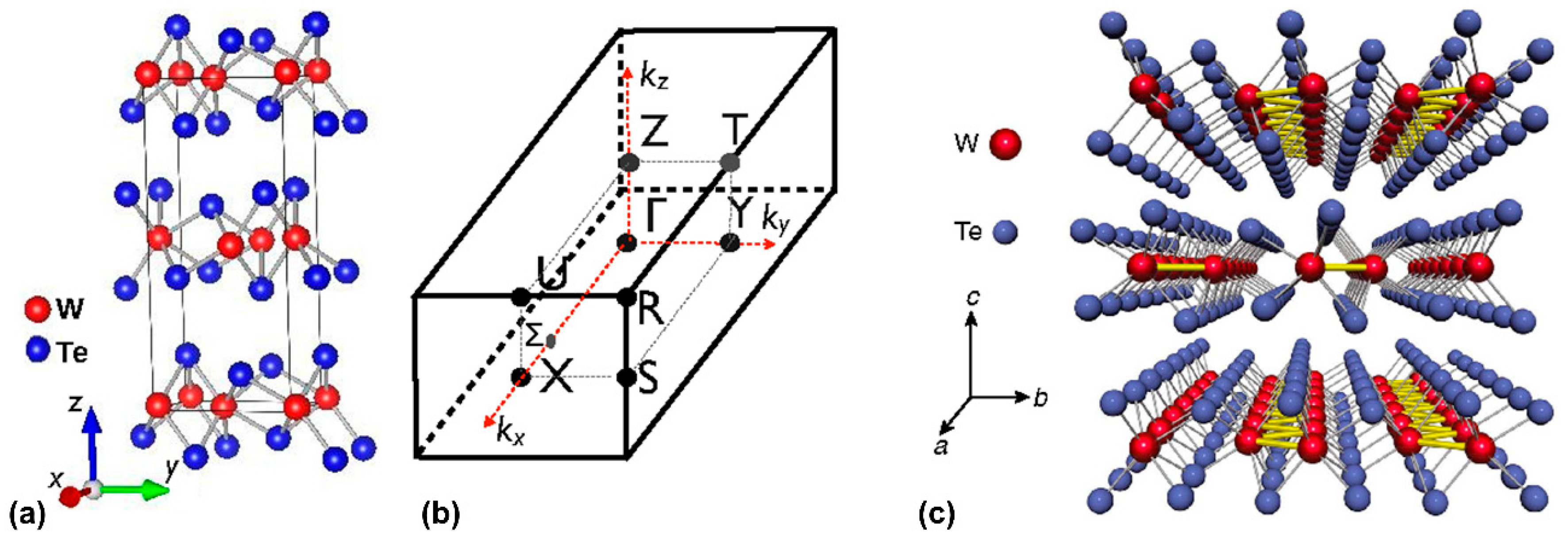
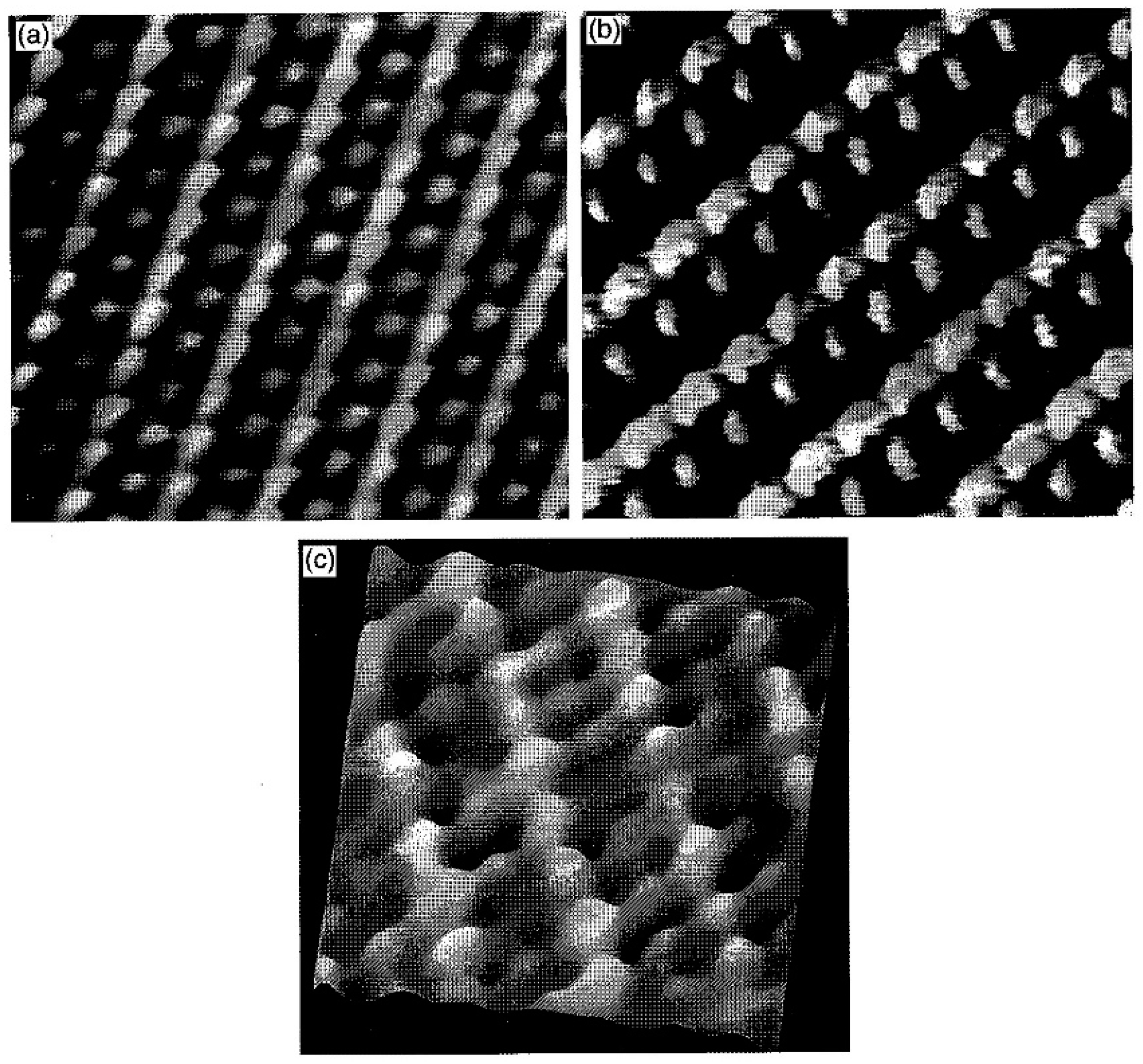
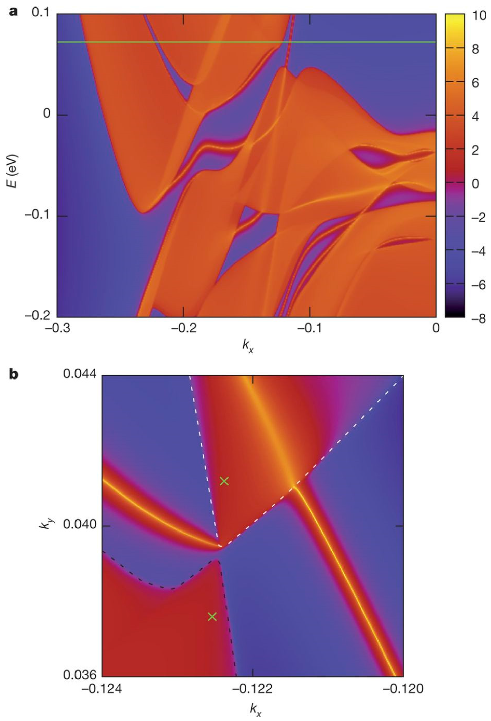
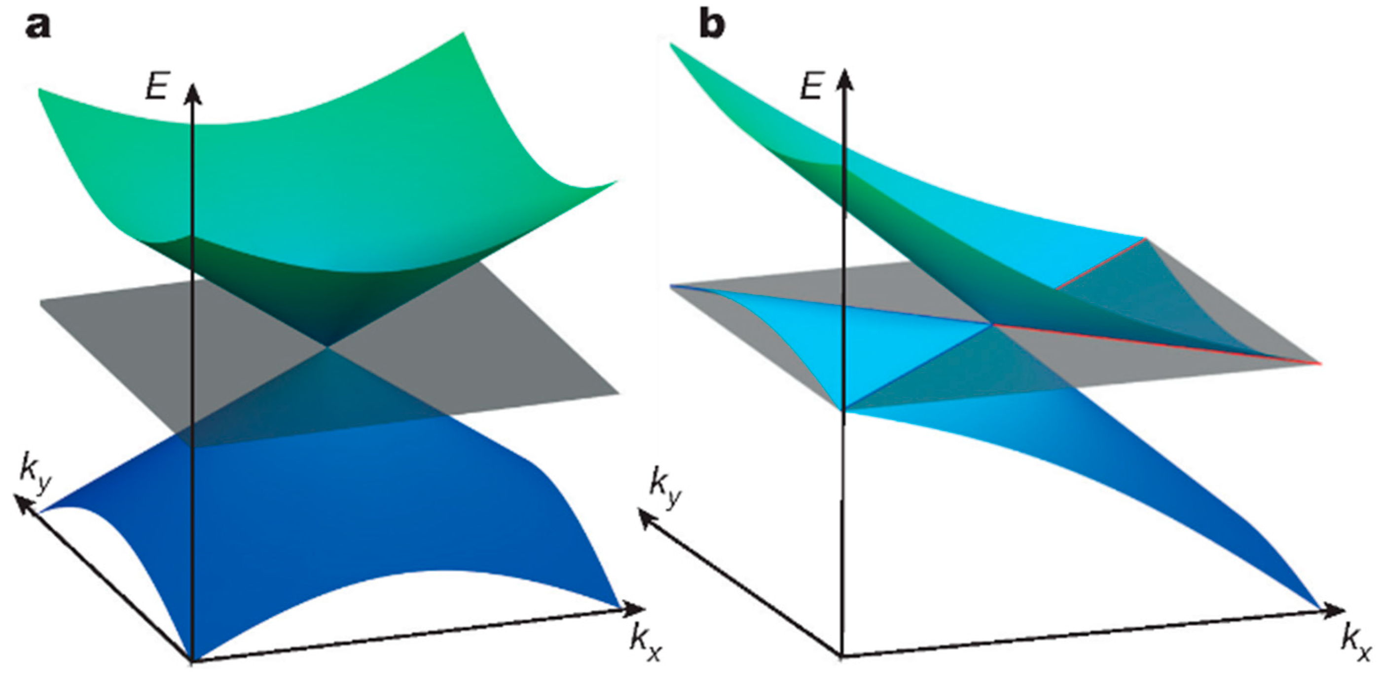
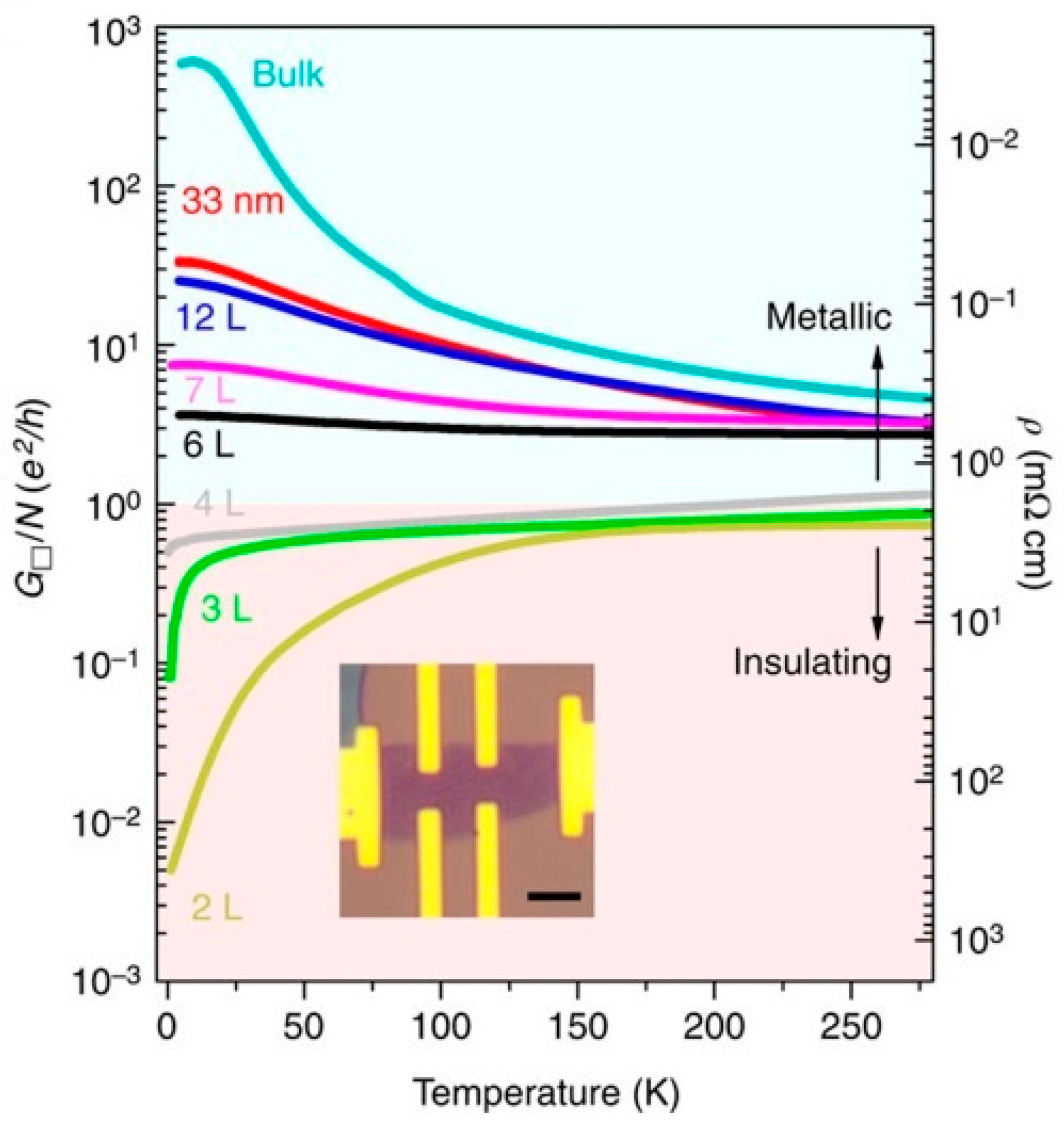
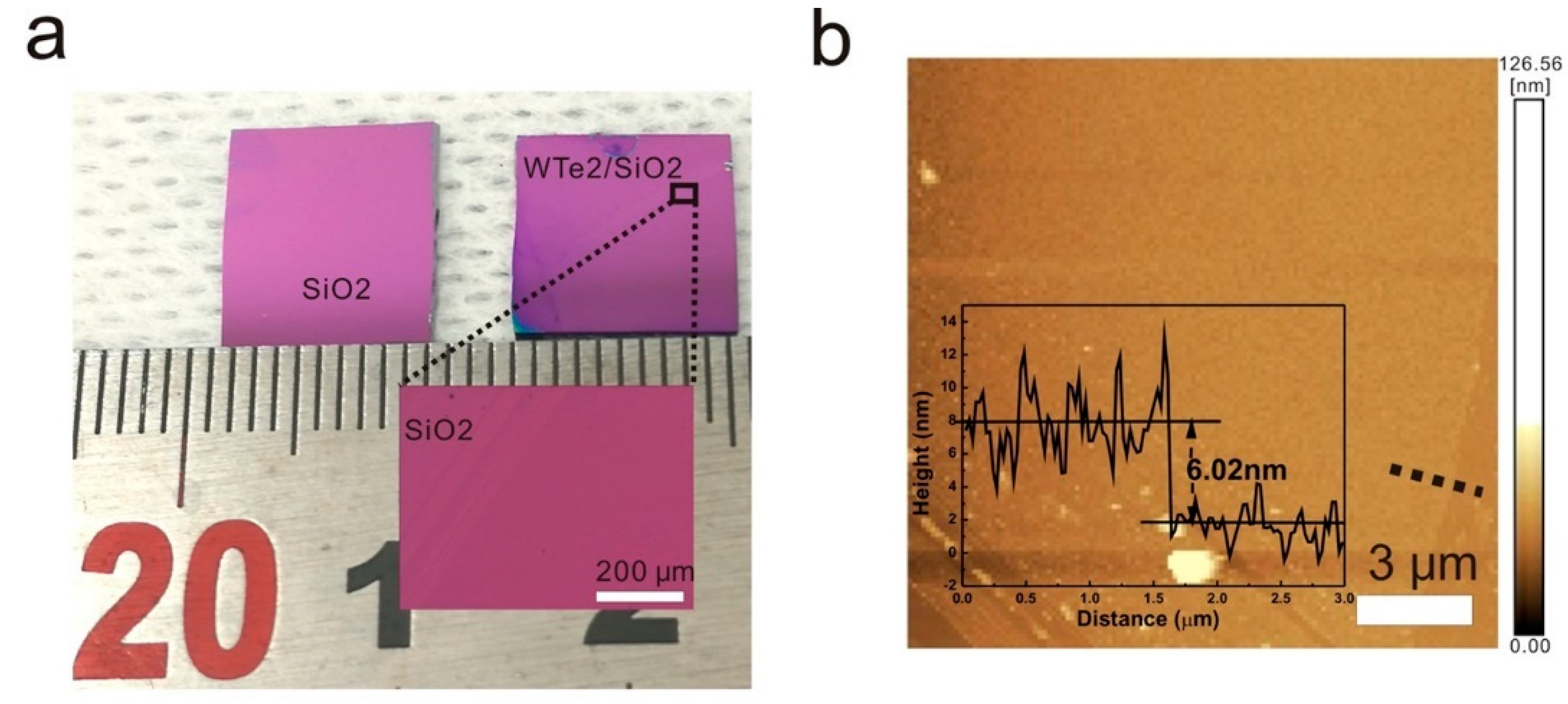
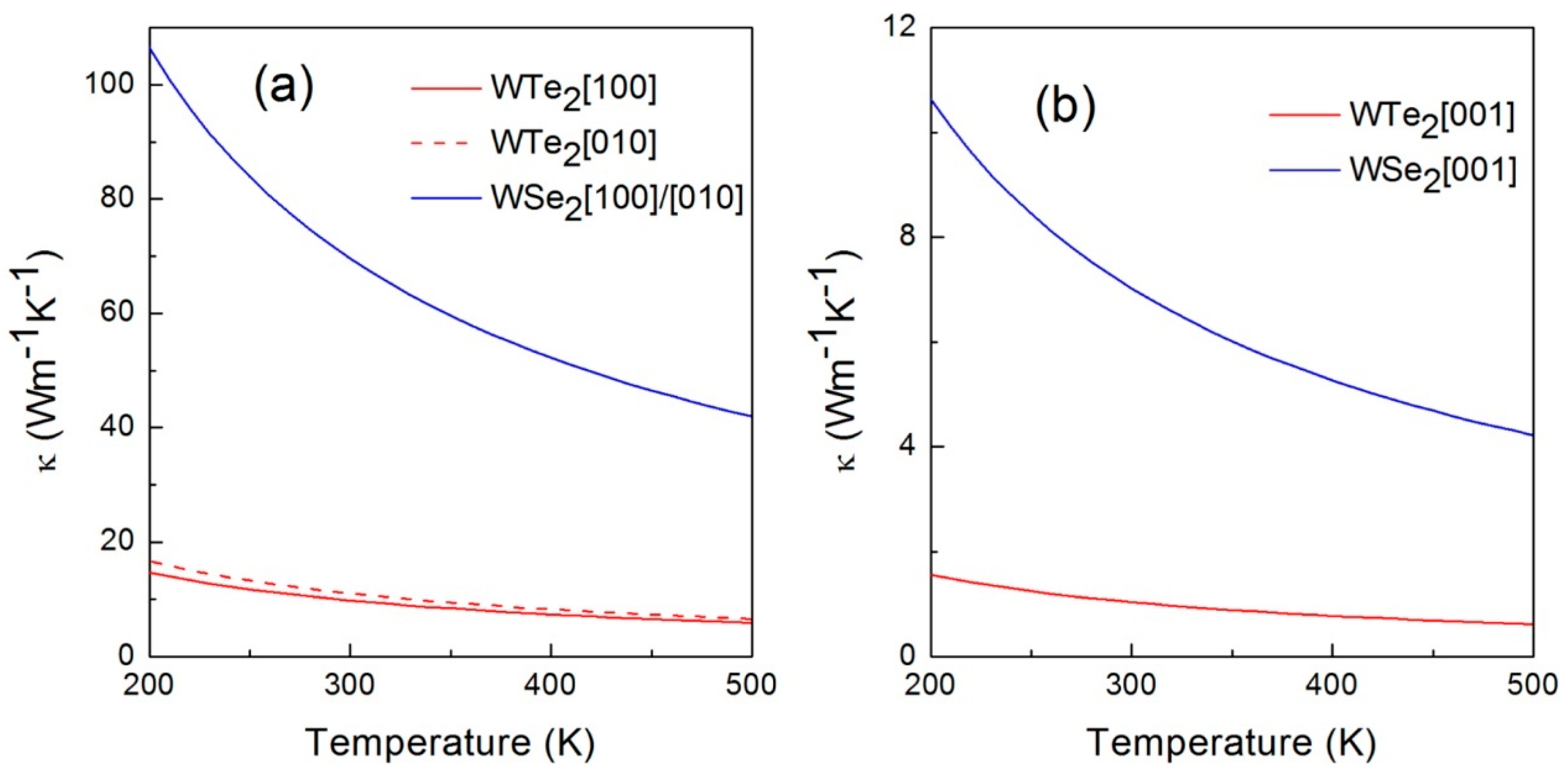
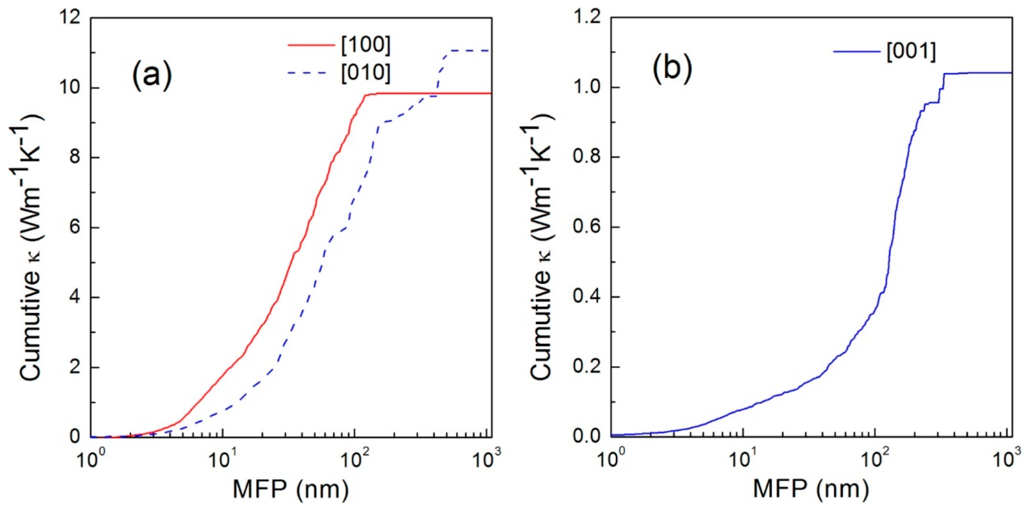
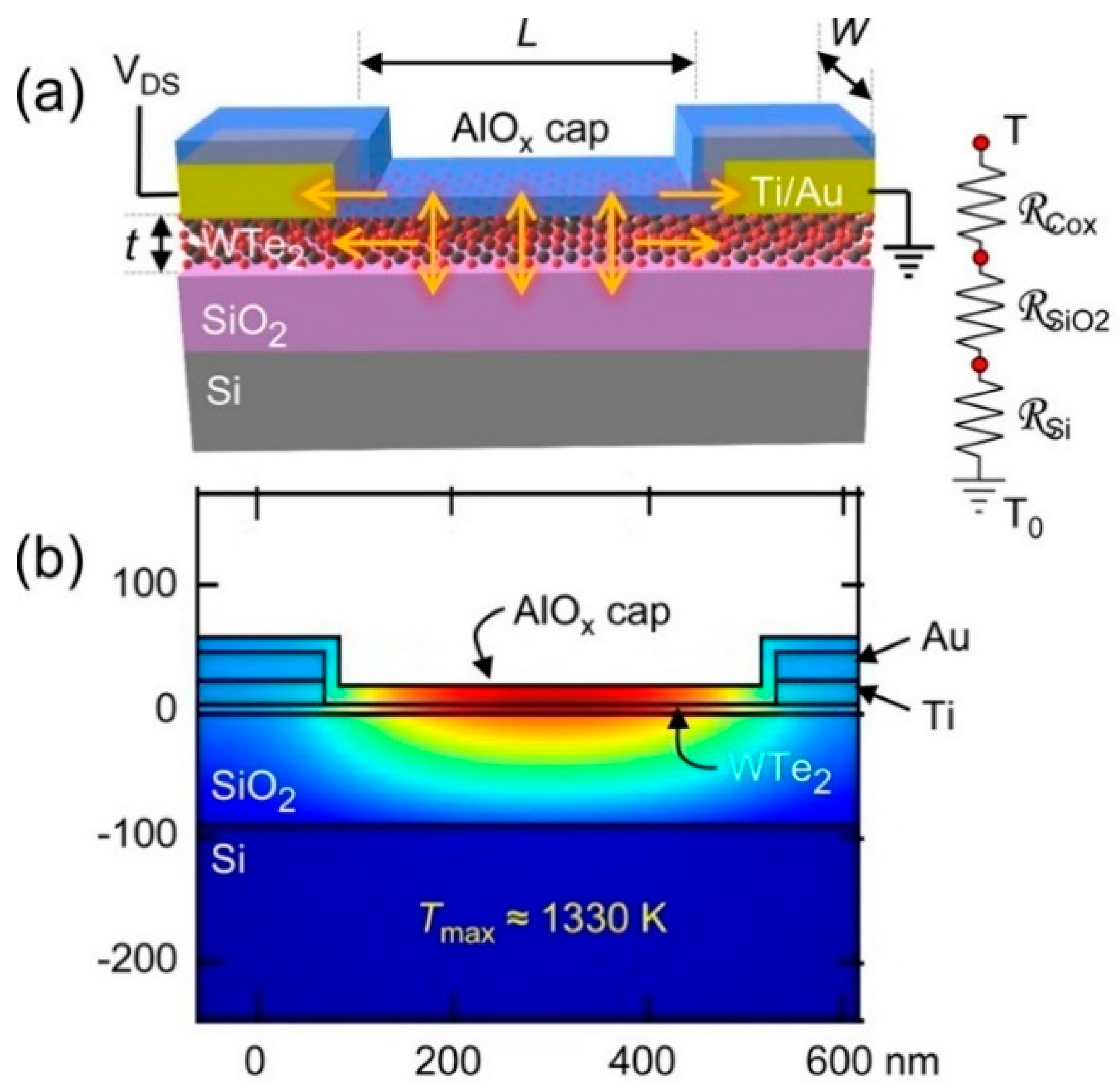
Table 1.
The thermal conductivities κ of WTe2 along different directions.
| Material | [100] (W·m−1·K−1) | [010] (W·m−1·K−1) | [001] (W·m−1·K−1) | T (K) | Methods | Ref. |
|---|---|---|---|---|---|---|
| Monolayer WTe2 | 9 | 20 | - | 300 | First-principle | [8] |
| Td-WTe2 | 9.03 | 7.69 | 0.46 | 300 | First-principle | [51] |
| Monolayer Td-WTe2 | 10 | 20 | - | 300 | First-principle | [52] |
| Atomically thin WTe2 | 2.5–3.5 to 9–11 in the [100] direction | 80–300 | Experiment | [7] | ||
| 4–20 layers Td-WTe2 flakes | 3–10 | 80–300 | Experiment and theory | [50] | ||
| Few-layer Td-WTe2 | 0.96–1.06 (total κ), 0.8 (mean κ) | 300–623 | Experiment | [53] | ||
| Polycrystalline WTe2 film | Less than 2 | 0.8 | 300 | Experiment | [42] | |
| Single-crystal WTe2 flake | 15 ± 3 | |||||
| WSe2 (62 nm thick) | 0.048 ([001], the lowest value in solid) | 300 | Experiment and simulation | [54] | ||
| Monolayer WSe2 | 50 | 50 | 6 | 300 | First-principle and theory | [63] |
| Single-crystal WSe2 platelets | 9.7 | 9.7 | 2.09 | 300 | Experiment | [64] |
| ReS2 flakes (60–450 nm) | 70 ± 18 | 50 ± 13 | 0.55 ± 0.07 | 300 | Experiment | [65] |
| MoS2 transistors | 14 ± 4 | 300 | Experiment | [66] | ||
| Single-layer h-BN | 600 | 300 | Numerical solution | [67] | ||
| Single-layer graphene | About (4840 ± 440) to (5300 ± 480) | 300 | Non-contact measurement | [68] | ||
© 2018 by the authors. Licensee MDPI, Basel, Switzerland. This article is an open access article distributed under the terms and conditions of the Creative Commons Attribution (CC BY) license (http://creativecommons.org/licenses/by/4.0/).
Share and Cite
MDPI and ACS Style
Tian, W.; Yu, W.; Liu, X.; Wang, Y.; Shi, J. A Review of the Characteristics, Synthesis, and Thermodynamics of Type-II Weyl Semimetal WTe2. Materials 2018, 11, 1185. https://0-doi-org.brum.beds.ac.uk/10.3390/ma11071185
AMA Style
Tian W, Yu W, Liu X, Wang Y, Shi J. A Review of the Characteristics, Synthesis, and Thermodynamics of Type-II Weyl Semimetal WTe2. Materials. 2018; 11(7):1185. https://0-doi-org.brum.beds.ac.uk/10.3390/ma11071185
Chicago/Turabian StyleTian, Wenchao, Wenbo Yu, Xiaohan Liu, Yongkun Wang, and Jing Shi. 2018. "A Review of the Characteristics, Synthesis, and Thermodynamics of Type-II Weyl Semimetal WTe2" Materials 11, no. 7: 1185. https://0-doi-org.brum.beds.ac.uk/10.3390/ma11071185
Note that from the first issue of 2016, this journal uses article numbers instead of page numbers. See further details here.