Nanosecond Laser Etching of Aluminum-Plated Composite Materials Applied to Frequency Selective Surfaces


Abstract
:1. Introduction
2. Experimental Procedure
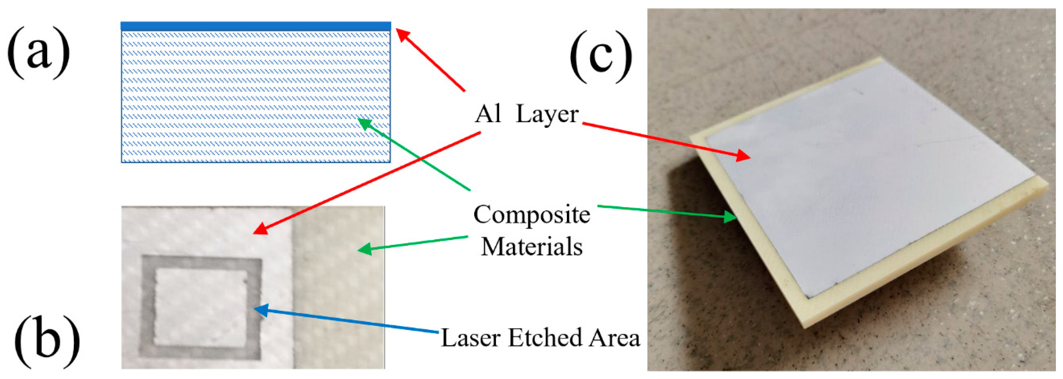
2.1. Materials
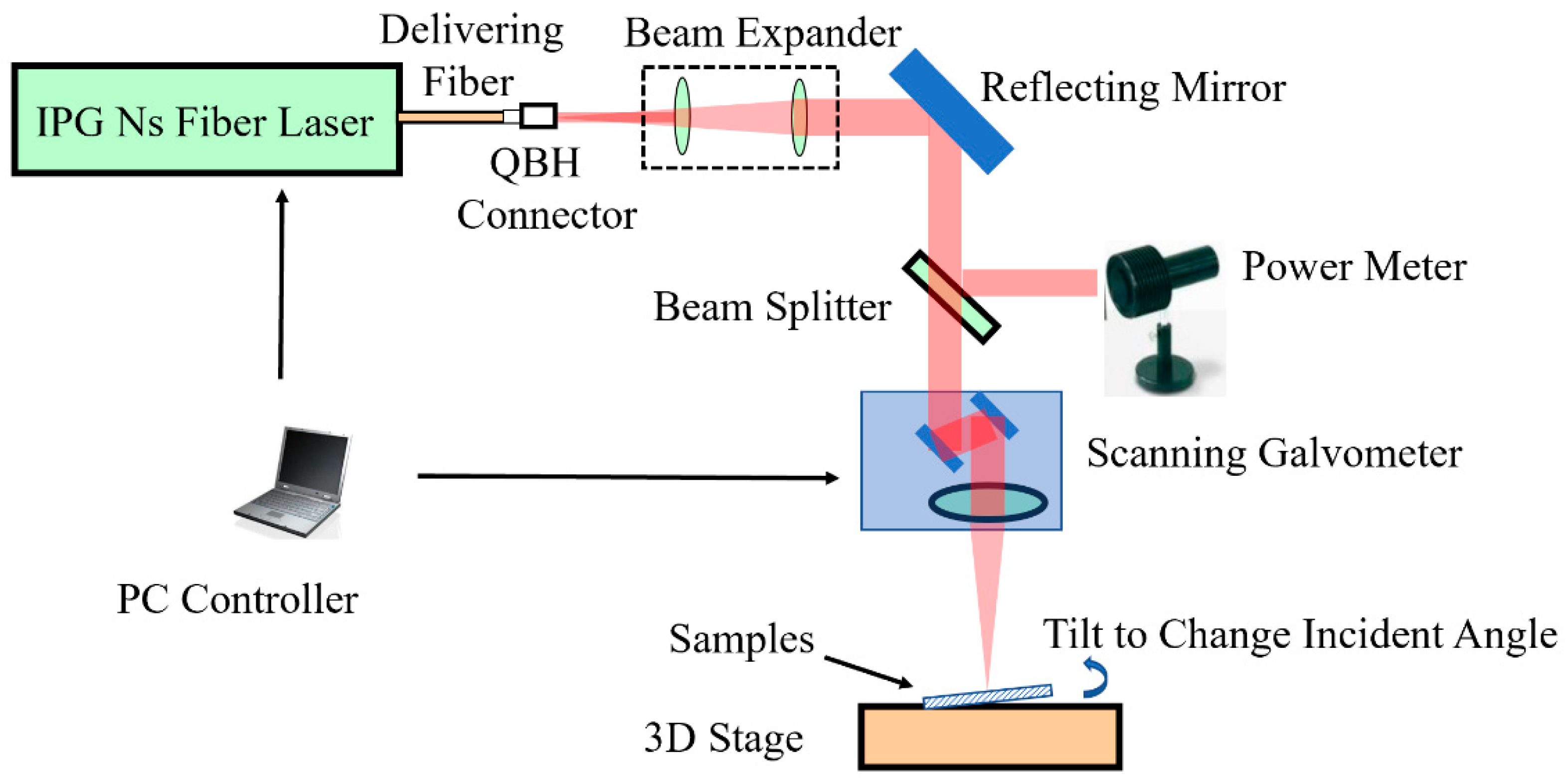
2.2. Experimental
3. Results and Discussion
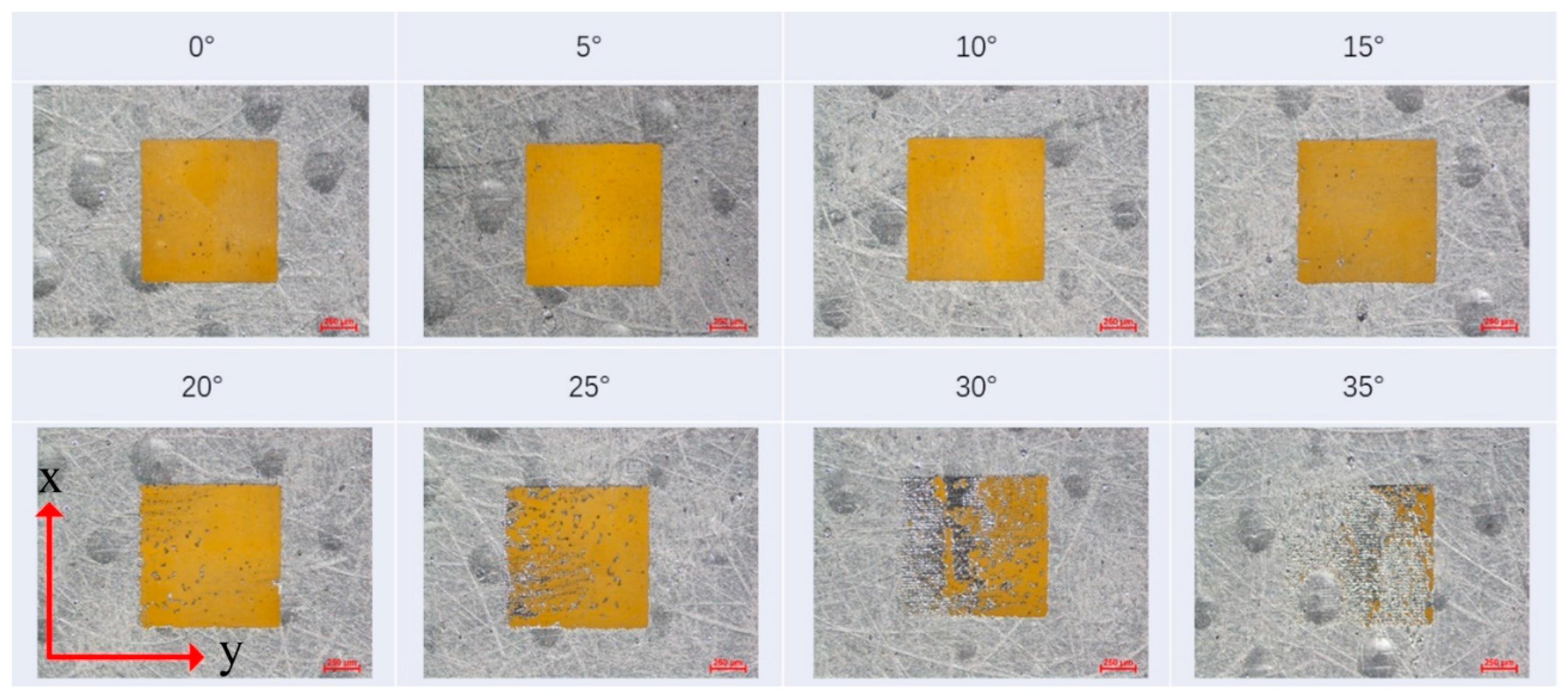
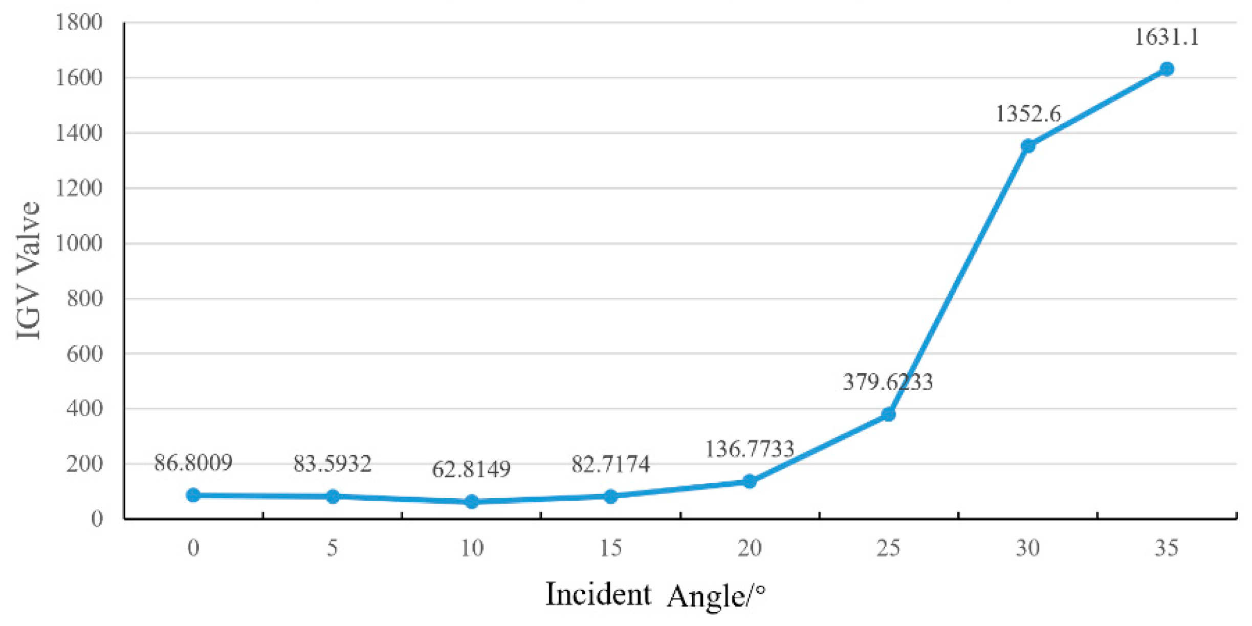
3.1. The Influence of Laser Incident Angle on Etching Quality and Accuracy
- (1)
- The polarization of the outcome laser beam was circular; thus, it should be irrelevant to the etching direction and result.
- (2)
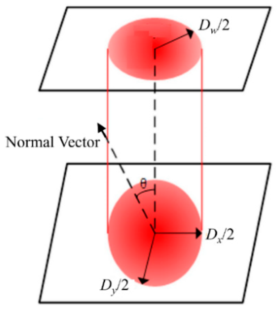
- When the laser light was normal to the surface (i.e., 0° of the incident angle), the projected area showed a circle shape. With the incident angle increasing, the projected area became elliptical, thus reducing the real laser fluence to the sample surface, as shown in Figure 5. In the figure, dw is the raw focused diameter, θ is the incident angle and dx and dy are the projected oval axis diameters. The reduction of laser fluence may have caused less etching depth. However, this variation was in the range of depth of focus, and the laser fluence was about six times that of the threshold fluence. For this situation, the fluence change due to the incident angle changing could be a minor factor.
- (3)
- The reflectivity of the surface may have changed, which could also have had some effect on the etching [29,30]. For example, Chang et al. argued that the reflectivity was kept consistent and had not much difference on the ablation phenomenon when the incident angle was below 20° [31]. Their conclusion fitted this study very well. With the incident angle going up further, it seemed there was an obvious jump of the reflectivity, thus causing uneven etching results. A very similar phenomenon was reported by Liao et al. when studying laser welding [30]. All the experimental results suggested there should be quite little reflectivity change when the incident angle breaks through a threshold value, and this change caused a worse processing quality.
- (4)
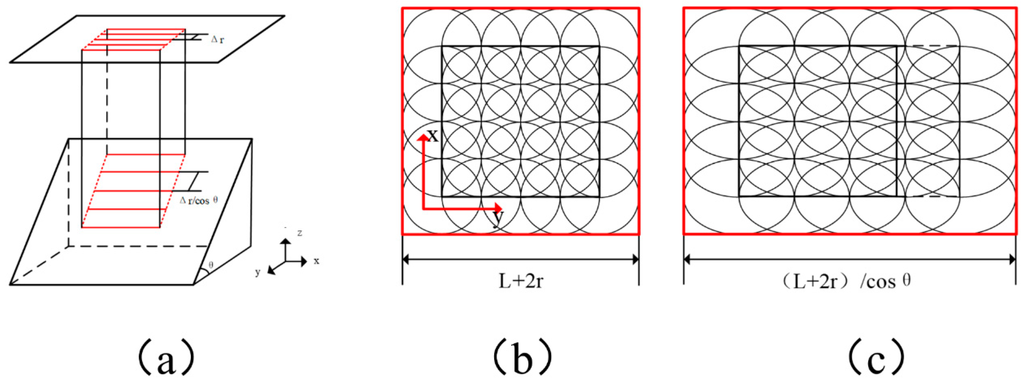
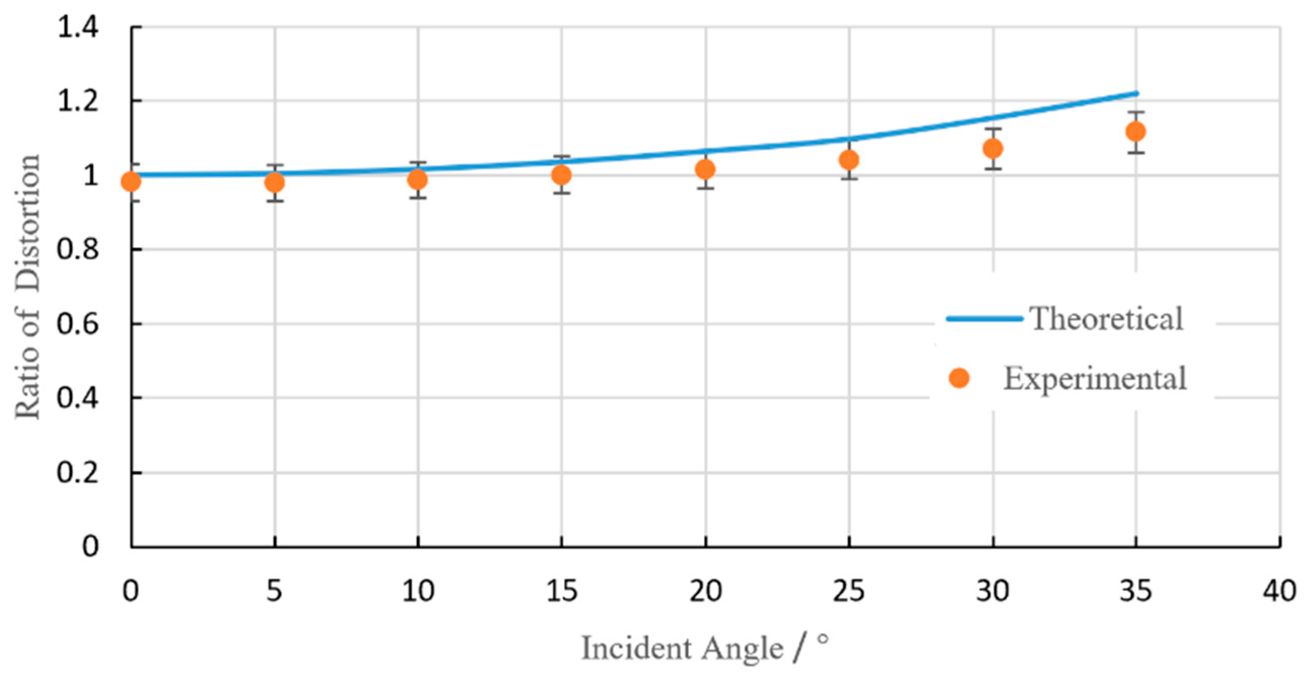
- When doing area etching, line-by-line hatching was usually adopted. With the incident angle varying, the hatch space was also affected (see Figure 6a for details). To simplify the situation, only the hatching distance in the y direction was elongated. After the projection transition, distortion happened: the square area changed to a rectangle. Consequently, the etching dimension in the y direction could have been affected from L + 2r to (L + 2r)/cosθ (see Figure 6b,c). In Figure 7, the calculated and measured dimension changes in the y direction are plotted, correspondingly. It can be seen that the measured experimental dimensions are smaller than the calculated ones. The smaller the incident angle was, the less the distortion was. The best coincidence was found at the incident angle of 10°.
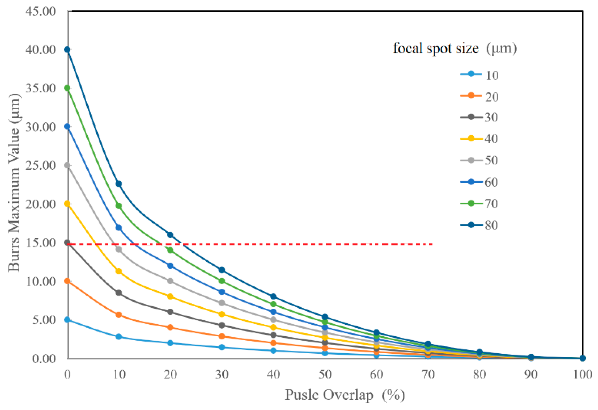
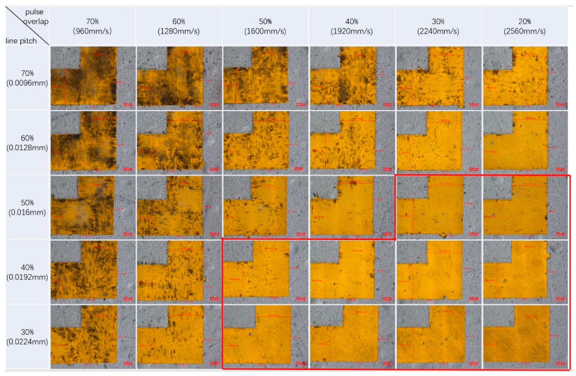
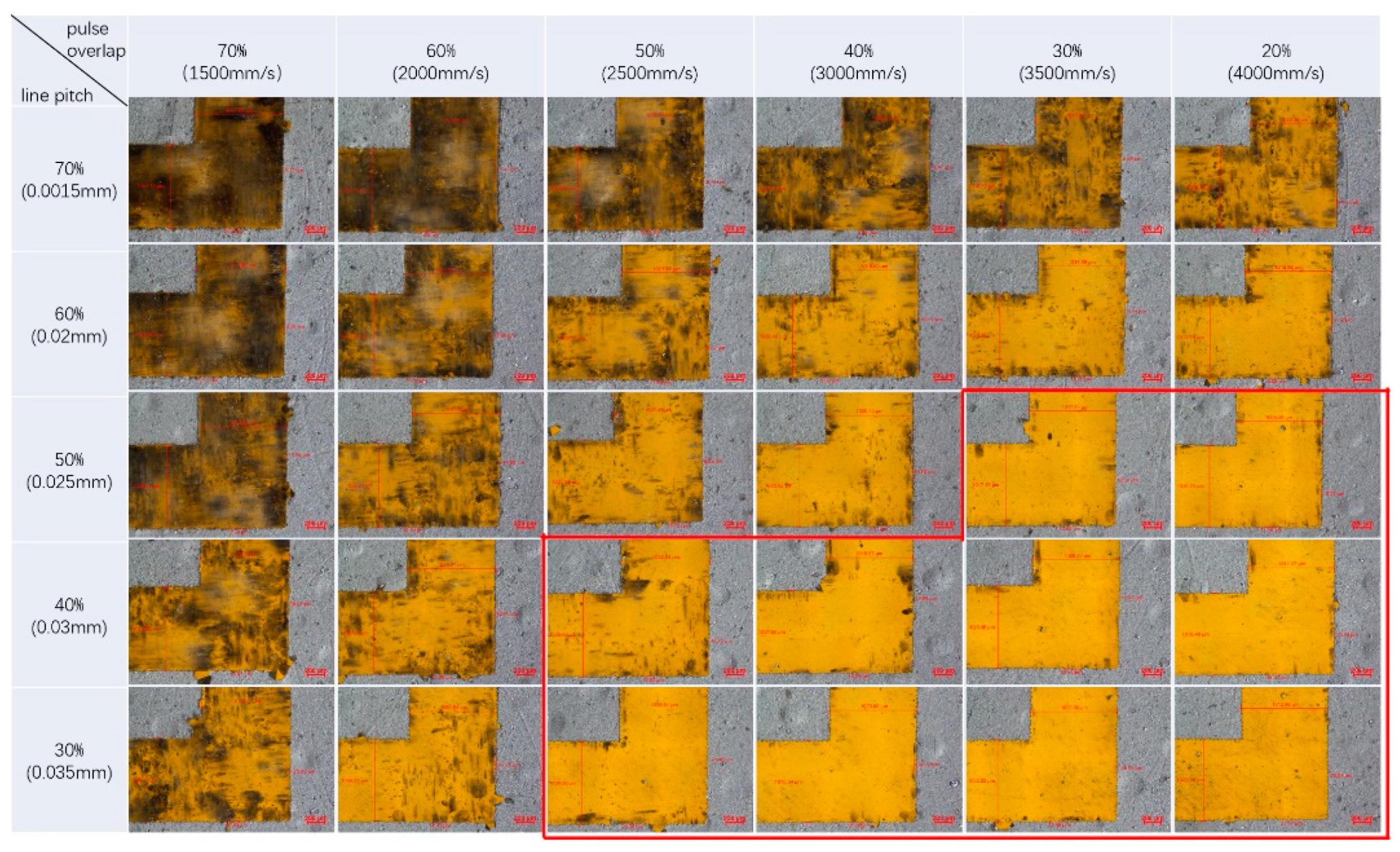
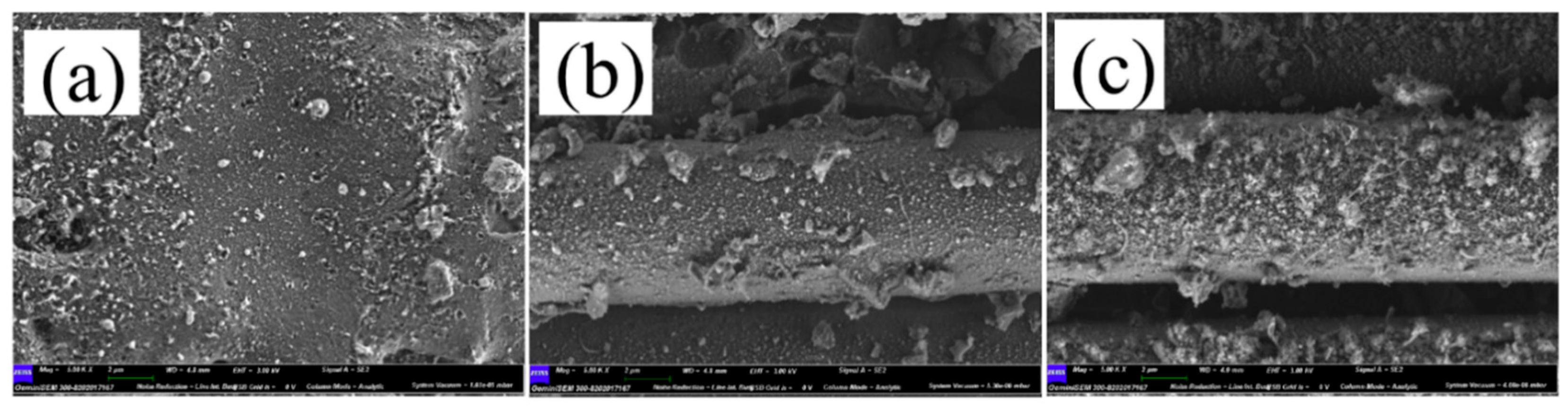
3.2. The Influence of Pulse Overlap and Focal Spot Size on Etching Uniformity and Base Materials
4. Conclusions
- The laser incident angle plays a pivotal role to guarantee FSS etching quality and accuracy. It is found that an incident angle range of ±15° is suitable for 20-μm aluminum-layer composite material etching within the depth of focus.
- As the laser incident angle changes, the variation of laser light reflectivity and hatch space between lines causes the etching quality instability.
- Laser pulse overlap and focal spot size affects not only etching border accuracy and uniformity but also the material removal consistence. Combining the theoretical and experimental results, it is inferred that the actual processing windows are smaller than of those calculated, when thermal effect and etching uniformity are considered.
- In order to ensure etching area uniformity and no damage to base materials, a pulse overlap of 30~50% and a relatively small focal spot size are recommended from the experimental results.
- By reasonably selecting a processing window, optimal etching results on FSSs with the nanosecond fiber laser could be obtained. The method and experimental techniques in this study could be generalized to different FSS material composition processing.
Author Contributions
Funding
Acknowledgments
Conflicts of Interest
References
- McLain, C.; Panthi, S.; Sturza, M.; Hetrick, J. High throughput Ku-band satellites for aeronautical applications. In Proceedings of the IEEE MILCOM 2012, Military Communications Conference, Orlando, FL, USA, 29 October–1 November 2012; pp. 1–6. [Google Scholar]
- Manikandan, E.; Sreeja, B.S.; Radha, S.; Duraiselvam, M.; Gupta, A.; Prabhu, S. Microfabrication of terahertz frequency-selective surface by short- and ultrashort laser ablation. Opt. Eng. 2019, 58, 011007. [Google Scholar]
- Tao, Y.; Zhao, Q.M.; Zhuang, L. Application of frequency selective surface technique in warship design. Warship 2013, 24, 26–28. (In Chinese) [Google Scholar]
- Qi, K.; Li, L.; Su, J.; Liu, Y.; Chen, J. Design of a tunable absorber based on active frequency-selective surface for UHF applications. Materials 2019, 12, 3989. [Google Scholar] [CrossRef] [PubMed] [Green Version]
- Paquay, M.; Iriarte, J.; Ederra, I.; Gonzalo, R.; Maagt, P. Thin AMC structure for radar cross-section reduction. IEEE Trans. Antennas Propag. 2007, 55, 3630–3638. [Google Scholar] [CrossRef]
- Shang, Y.; Shen, Z.; Xiao, S. Frequency-selective rasorber based on square-loop and cross-dipole arrays. IEEE Trans. Antennas Propag. 2014, 62, 5582–5589. [Google Scholar] [CrossRef]
- Li, A.; Singh, S.; Sievenpiper, D. Metasurfaces and their applications. Nanophotonics 2018, 7, 989–1011. [Google Scholar] [CrossRef]
- Princy, S.S.; Sreeja, B.S.; Manikandan, E.; Radha, S.; Prabhu, S.S. An ultrafast laser micromachined broadband terahertz frequency selective surface. Bull. Mater. Sci. 2019, 42, 151. [Google Scholar] [CrossRef] [Green Version]
- Zhang, X.; Wu, W.; Li, C.; Wang, C.; Ma, Y.; Yang, Z.; Sun, G.; Yuan, N. A dual-band terahertz absorber with two passbands based on periodic patterned graphene. Materials 2019, 12, 3016. [Google Scholar] [CrossRef] [PubMed] [Green Version]
- Li, Y.; Ren, P.; Xiang, Z. A dual-passband frequency selective surface for 5G communication. IEEE Antenn. Wirel. Propag. Lett. 2019, 18, 2597–2601. [Google Scholar] [CrossRef]
- Liu, T.; Kim, S.S. Design of wide-bandwidth electromagnetic wave absorbers using the inductance and capacitance of a square loop-frequency selective surface calculated from an equivalent circuit model. Opt. Commun. 2016, 359, 372–377. [Google Scholar] [CrossRef]
- Liu, T.; Kim, S.S. Design of ultrawide bandwidth double-layer electromagnetic wave absorbers with square-loop frequency selective surfaces. Microw. Opt. Technol. Lett. 2018, 60, 2013–2018. [Google Scholar] [CrossRef]
- Li, W.; Chen, M.; Zeng, Z. Broadband composite radar absorbing structures with resistive frequency selective surface: Optimal design, manufacturing and characterization. Compos. Sci. Technol. 2017, 145, 10–14. [Google Scholar] [CrossRef]
- Manikandan, E.; Sreeja, B.S.; Radha, S.; Bathe, R.N. Direct laser fabrication of five-band symmetric terahertz metamaterial with Fano Resonance. Mater. Lett. 2018, 229, 320–323. [Google Scholar] [CrossRef]
- Ai, J.; Xiang, H.Q.; Du, Q.F.; Chen, D.C.; Liu, J.G.; Zeng, X.Y. Rapid and high-performance processing technology for large-area frequency selective surfaces. J. Mater. Proc. Technol. 2019, 264, 129–133. [Google Scholar] [CrossRef]
- Zhu, M.; Wang, H.Q.; Wang, Z.L. Digital robot machining key technologies for complex frequency selective surfaces. Astro Manuf. Technol. 2005, 1, 61–63. [Google Scholar]
- Moallem, M.; Sarabandi, K. Miniaturized-element frequency selective surfaces for millimeter-wave to terahertz applications. IEEE Trans. Terahertz Sci. Technol. 2012, 2, 333–339. [Google Scholar] [CrossRef]
- Diaci, J.; Bracun, D.; Gorkic, A.; Mozina, J. Rapid and flexible laser marking and engraving of tilted and curved surfaces. Opt. Lasers Eng. 2011, 49, 195–199. [Google Scholar] [CrossRef]
- Kim, J.; Kang, C.; Hong, S. Electromagnetic wave characteristics of composite frequency selective surfaces with patch-grid-patch type structure fabricated by e-beam deposition. Polym. Compos. 2020, 41, 1100–1105. [Google Scholar] [CrossRef]
- Jaiswar, R.; Mederos-Henry, F.; Dupont, V.; Hermans, S.; Raskin, J.P.; Huynen, I. Inkjet-printed frequency-selective surfaces based on carbon nanotubes for ultra-wideband thin microwave absorbers. J. Mater. Sci. Mater. Electron. 2020, 31, 2190–2201. [Google Scholar] [CrossRef]
- Wang, C.; Zeng, X.Y. Study of laser carving three-dimensional structures on ceramics: Quality controlling and mechanisms. Opt. Laser Technol. 2007, 39, 1400–1405. [Google Scholar] [CrossRef]
- Zhang, G.X.; Hua, X.M.; Huang, Y.; Zhang, Y.L.; Li, F.; Shen, C.; Cheng, J. Investigation on mechanism of oxide removal and plasma behavior during laser cleaning on aluminum alloy. Appl. Surf. Sci. 2020, 506, 144666. [Google Scholar] [CrossRef]
- Zhang, H.W.; Ren, N.; Xue, H.T.; Tang, F.L.; Yan, X.D.; Lu, W.J.; Liu, X.L. Temperature distribution for laser etching of metal thin films on polyimide substrate. Chin. J. Lasers 2016, 43, 0503009. [Google Scholar] [CrossRef]
- Esakkimuthu, M.; Suseela, S.B.; Sankarrajan, R.; Gupta, A.; Prabhu, S. Microfabrication of low cost frequency selective surface for terahertz wave by laser ablation. J. Electron. Mater. 2019, 48, 2423–2429. [Google Scholar] [CrossRef]
- Cheng, J.; Perrie, W.; Sharp, M.; Edwardson, S.P.; Semaltianos, N.G.; Dearden, G.; Watkins, K.G. Single-pulse drilling study on Au, Al and Ti alloy by using a picosecond laser. Appl. Phys. A Mater. 2009, 95, 739–746. [Google Scholar] [CrossRef]
- Zhang, H.Z.; Zhang, C.Y.; Wang, H.Y.; Liu, F.F. Ablation behavior of SiCp/AA2024 composites irradiated by a single-pulse nanosecond laser. Opt. Laser Technol. 2020, 126, 106075. [Google Scholar] [CrossRef]
- Steen, W.M. Laser Material Processing, 3rd ed.; Springer: London, UK, 2003; pp. 94–95. [Google Scholar]
- Hassaballah, M.; Kanazawa, T.; Ido, S. Efficient eye detection method based on grey intensity variance and independent components analysis. IET Comput. Vis. 2010, 4, 261–271. [Google Scholar] [CrossRef]
- Zuhlke, C.A.; Tsibidis, G.D.; Anderson, T.; Stratakis, E.; Gogos, G.; Alexander, D.R. Investigation of femtosecond laser induced ripple formation on copper for varying incident angle. AIP Adv. 2018, 8, 015212. [Google Scholar] [CrossRef] [Green Version]
- Liao, Y.C.; Yu, M.H. Effects of laser beam energy and incident angle on the pulse laser welding of stainless-steel thin sheet. J. Mater. Proc. Technol. 2007, 190, 102–108. [Google Scholar] [CrossRef]
- Chang, H.; Jin, X.; Zhou, W.J. Experimental investigation of plume expansion dynamics of nanosecond laser ablated Al with small incident angle. Optik 2014, 125, 2923–2926. [Google Scholar] [CrossRef]
- Cheng, J.; Perrie, W.; Edwardson, S.P.; Fearon, E.; Dearden, G.; Watkins, K.G. Effects of laser operating parameters on metals micromachining with ultrafast lasers. Appl. Surf. Sci. 2009, 256, 1514–1520. [Google Scholar] [CrossRef]


| Spot Size (μm) | Pulse Width (ns) | Repetition Rate (kHz) | Scanning Speed (mm/s) | Peak Power (Mw) | Peak Fluence (J/cm2) |
|---|---|---|---|---|---|
| 32 | 100 | 100 | 1920 | 16.6 | 20.64 |
| Spot Size (μm) | Pulse Width (ns) | Repetition Rate (kHz) | Scanning Speed (mm/s) | Peak Power (Mw) | Peak Fluence (J/cm2) |
|---|---|---|---|---|---|
| 32 | 100 | 100 | 960–2560 | 16.6 | 20.64 |
| 50 | 100 | 100 | 1000–4000 | 39.8 | 20.27 |
© 2020 by the authors. Licensee MDPI, Basel, Switzerland. This article is an open access article distributed under the terms and conditions of the Creative Commons Attribution (CC BY) license (http://creativecommons.org/licenses/by/4.0/).
Share and Cite
Cheng, J.; Jing, S.; Lou, D.; Yang, Q.; Tao, Q.; Zheng, Z.; Chen, L.; Yang, X.; Liu, D. Nanosecond Laser Etching of Aluminum-Plated Composite Materials Applied to Frequency Selective Surfaces. Materials 2020, 13, 2808. https://0-doi-org.brum.beds.ac.uk/10.3390/ma13122808
Cheng J, Jing S, Lou D, Yang Q, Tao Q, Zheng Z, Chen L, Yang X, Liu D. Nanosecond Laser Etching of Aluminum-Plated Composite Materials Applied to Frequency Selective Surfaces. Materials. 2020; 13(12):2808. https://0-doi-org.brum.beds.ac.uk/10.3390/ma13122808
Chicago/Turabian StyleCheng, Jian, Shufeng Jing, Deyuan Lou, Qibiao Yang, Qing Tao, Zhong Zheng, Lie Chen, Xuefeng Yang, and Dun Liu. 2020. "Nanosecond Laser Etching of Aluminum-Plated Composite Materials Applied to Frequency Selective Surfaces" Materials 13, no. 12: 2808. https://0-doi-org.brum.beds.ac.uk/10.3390/ma13122808