Dielectric Response and Structural Analysis of (A3+, Nb5+) Cosubstituted CaCu3Ti4O12 Ceramics (A: Al and Bi)


1
Department of Physics, College of Science, King Faisal University, P.O. Box 400, Al-Ahsa 31982, Saudi Arabia
2
Physics Department, Faculty of Science, Assiut University, Assiut 71516, Egypt
3
Department of Physics, Faculty of Science, The New Valley University, El-Kharga 72511, Egypt
4
Department of Applied Molecular Chemistry, College of Industrial Technology, Nihon University, Narashino, Chiba 275-8575, Japan
*
Author to whom correspondence should be addressed.
Materials 2020, 13(24), 5822; https://0-doi-org.brum.beds.ac.uk/10.3390/ma13245822
Submission received: 1 November 2020
/
Revised: 11 December 2020
/
Accepted: 14 December 2020
/
Published: 21 December 2020
(This article belongs to the Special Issue Oxide-Based Materials for Energy Storage and Conversion)
Abstract
:CaCu3Ti4-x((A0.05Nb0.05))xO12 ceramics (A: Al and Bi; x = 0, 0.3) were synthesized by high-energy mechanical ball milling and reactive sintering at 1050 °C in air. Rietveld refinement of XRD data revealed the pure and (Al3+, Nb5+) cosubstituted ceramics contained a minor CuO secondary phase with a mole fraction of about 3.2% and 6.9%, respectively, along with a CaCu3Ti4O12 (CCTO)-like cubic structure. In addition, (Bi3+, Nb5+) cosubstituted ceramics had a pyrochlore (Ca2(Ti, Nb)2O7) secondary phase of about 18%. While the (Al3+, Nb5+) cosubstituted CCTO showed the highest relative permittivity (ε’ = 3.9 × 10⁴), pure CCTO showed the lowest dielectric loss (tanδ = 0.023) at 1 kHz and 300 K. Impedance-spectroscopy (IS) measurements showed an electrically heterogeneous structure for the studied ceramics, where a semiconducting grain was surrounded by highly resistive grain boundary. The giant relative permittivity of the ceramics was attributed to the Maxwell–Wagner polarization effect at the blocking grain boundaries and domain boundaries. The higher tanδ of the cosubstituted samples was correlated with their lower grain boundary’s resistivity, as confirmed by IS analysis. Modulus-spectrum analysis revealed two relaxation processes for the pure and (Bi3+, Nb5+) cosubstituted CCTO samples. Dissimilar behavior was observed for the (Al3+, Nb5+) cosubstituted CCTO, where three relaxation mechanisms were observed and attributed to the grain, domain-boundary, and grain-boundary responses.
1. Introduction
Materials with colossal relative permittivity (ε’ > 103) are important for numerous energy-storage-related applications. In this regard, one of the most promising materials is CaCu3Ti4O12 (CCTO) due to its specific dielectric properties. The relative permittivity of CCTO can attain giant values of 104–106 with little dependency on temperature and frequency of measurement [1]. The origin of the dielectric properties of CCTO is still controversially discussed in the literature. Several studies evidenced an electrically inhomogeneous structure for CCTO and its related materials, i.e., semiconductor grains surrounded by insulating grain boundaries [2]. Considering this polycrystalline structure for CCTO, the model of the internal barrier layer capacitor (IBLC) was proposed by Sinclair et al. [3] and was successfully used in the literature to interpret the dielectric behavior of CCTO. According to this model, the colossal ε’ of CCTO near room temperature and low frequency is due to the extrinsic effect related to Maxwell–Wagner (M–W) polarization at the internal resistive boundaries, such as grain boundaries and/or domain boundaries [4,5]. At a high frequency of the applied electric field, charge accumulation at the internal boundaries was reduced; hence, a decrease in ε′ was observed. An additional extrinsic effect from the sample/electrode interface was also suggested to contribute to the colossal permittivity of CCTO and its related materials [3]. Nevertheless, the use of CCTO as a dielectric material in technology is hindered by its high dielectric loss (tanδ > 0.05). Therefore, research continues for better understanding and improving the dielectric response of CCTO, and to suggest alternative colossal permittivity dielectric materials. In this regard, several strategies are being implemented, such as doping, substitution, and controlling synthesis conditions [6,7,8,9,10,11,12,13,14,15,16,17]. In particular, cosubstitution for Ti4+ with heterovalent elements was reported as a promising technique to reduce tanδ without degrading the ε’ of TiO2 and CCTO ceramics [12,18,19,20,21]. For instance, (Al3+, Nb5+) cosubstituents resulted in the increased relative permittivity (ε’ ≈ 2.9−4.1 × 10⁴) and decreased dielectric loss (tanδ ≈ 0.045–0.058) of CCTO ceramics [12]. Ceramics in [12] were prepared by a solid-state reaction process comprising a calcination step at 850 °C for 12 h and conventional sintering at 1050–1090 °C for 3–36 h. Several mechanisms were proposed to explain the colossal relative permittivity of the cosubstituted CCTO, including the confinement of charge-carrier hopping by extrinsic defect clusters [20,22] and the formation of internal capacitors at the internal boundaries of the ceramic (IBLC model) [12]. According to the IBLC model, the colossal permittivity of the ceramics is a result of the internal capacitances that form due to the accumulation of charge carriers at the internal resistive boundaries of the tested sample [3]. Considering this structure, the static relative permittivity of IBLC ceramics depends on the thickness of the grain boundary (tg.b.), the average grain size (tg), and the relative permittivity of the grain boundary (εr), as follows [23,24]:
In the present work, we investigated the structural and dielectric properties of cosubstituted CCTO with the composition of CaCu3Ti4−x[(A0.05Nb0.05)]xO12 (A: Al and Bi; x = 0, 0.3). The investigated ceramics were prepared by a simple reactive solid-state reaction process where the calcination step was dismissed. The reactive sintering process has the advantages of having lower thermal budget and more control on the grain size of the final ceramics [14]. To the best of our knowledge, there are no previous reports on the dielectric properties of (Bi3+, Nb5+) or (Al3+, Nb5+)-cosubstituted CCTO ceramics prepared by reactive sintering. Few reports exist on (Al3+, Nb5+)-cosubstituted CCTO ceramics prepared by conventional solid-state reaction [12]. The structural and microstructural properties of the prepared ceramics were studied using X-ray diffraction and FE-SEM measurements. The dielectric properties of the prepared ceramics were studied in a wide range of frequencies (1 Hz–10 MHz) and temperatures (120–400 K).
2. Materials and Methods
Powders of CaCu3Ti4−x((A0.05Nb0.05))xO12 (A: Al and Bi; x = 0, 0.3) were synthesized using mechanochemical milling (Fritsch P-7 premium line machine). Stoichiometric amounts of high-purity CaCO3, CuO, TiO2, Nb2O5, Bi2O3, and Al2O3 were ball-milled with 2-propanol as the medium for 20 h at a rotation speed of 600 rpm. The mass ratio of grinding balls to powder was 8:1. After drying the mixture at 200 °C for 12 h, about 0.5 g of the obtained powder was pressed at pressure of 200 MPa for 3 min using a uniaxial hydraulic press. The obtained green pellet was then sintered in air at 1050 °C for 15 h. Prepared samples are referred to as CCTO, CCTANO, and CCTBNO. Field-emission scanning electron microscope (FE-SEM) (Joel, SM7600F, Tokyo, Japan) was used to study the microstructure of the ceramics. X-ray diffraction (XRD) measurements in the range of 10° ≤ 2θ ≤ 90° were collected using a Bruker D8 Advance X-ray powder diffractometer (CuKα radiation, Karlsruhe, Germany). A turnkey concept 50 system from Novocontrol was used for impedance-spectroscopy (IS) measurements over the 1 Hz–10 MHz frequency range and 120–400 K temperature range in a dry nitrogen atmosphere. Sputtered gold electrodes were used for electrical measurements.
3. Results
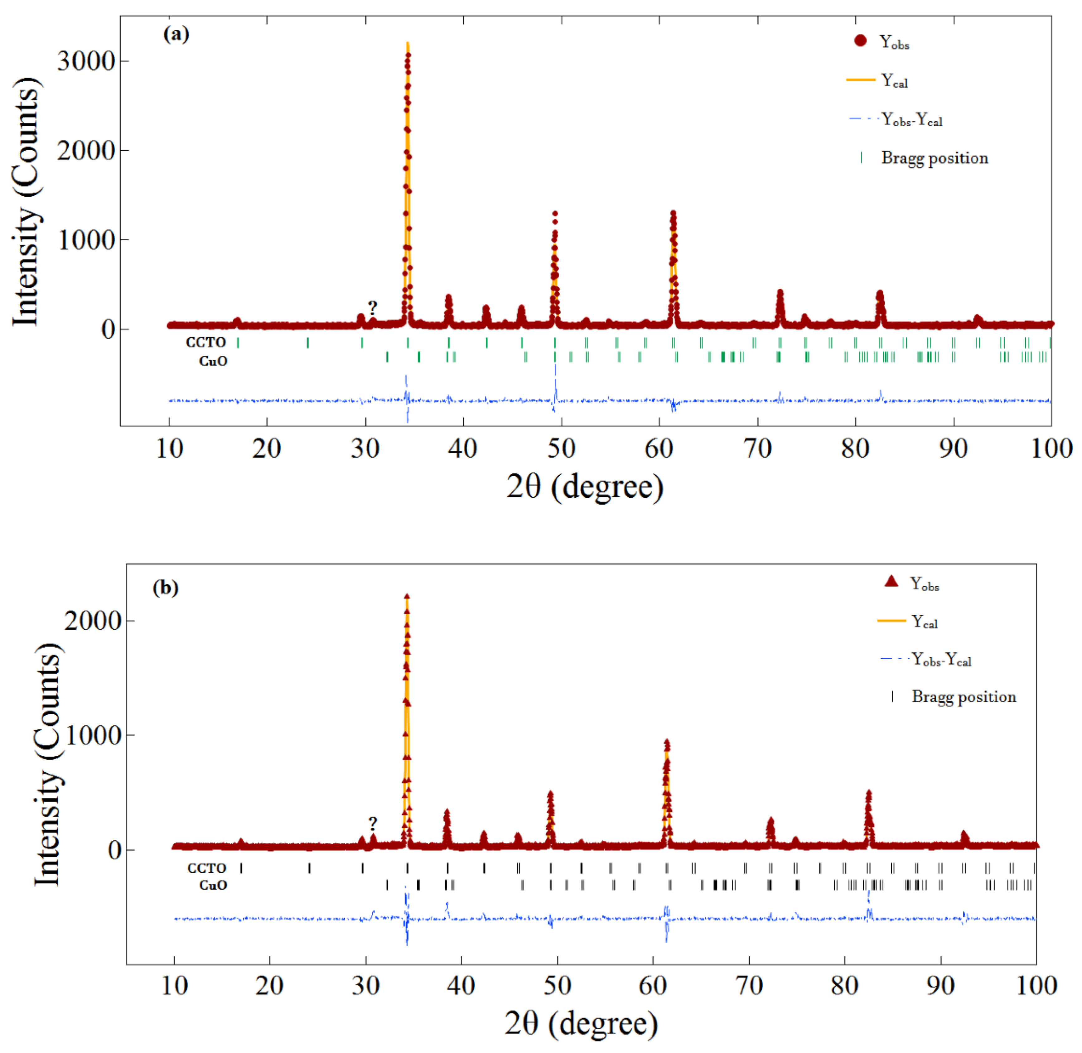
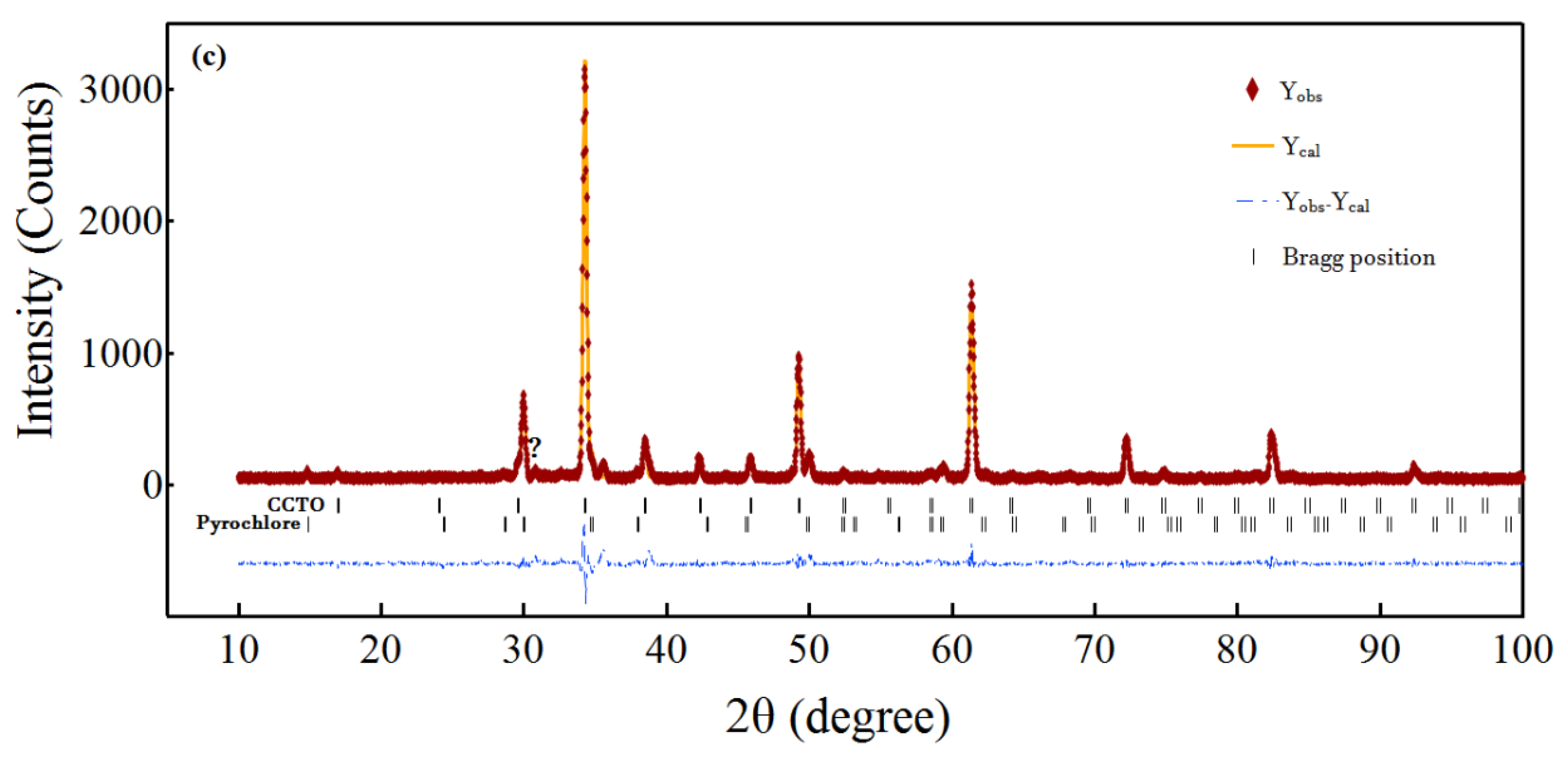
The X-ray diffraction pattern of the powder (not shown here) showed the onset of formation of a CCTO-like cubic phase during the mechanical milling step. The diffraction patterns of the ceramic samples are shown in Figure 1. Though the majority of diffraction peaks for all ceramics could be indexed as a CCTO cubic phase (JCPDS file no. 75–2188), additional peaks of other secondary phases were observed. Therefore, the Rietveld refinement method was deployed using RIETAN-2000 software [25] to elucidate the structural parameters, and to identify and determine the percentage of the secondary phase. The refined structure parameters and agreement factors of the profile are shown in Table 1. The pure and CCTANO ceramics contained a minor CuO secondary phase with a mole fraction of about 3.2% and 6.9%, respectively. CCTBNO showed a considerable pyrochlore (Ca2(Ti, Nb)2O7) secondary phase of about 18%. Moreover, CCTBNO ceramics showed an increased lattice parameter compared to that of CCTO due to the larger ionic radius of dopants Nb5+ (69 pm) and Bi3+ (96 pm) compared to Ti4+ (61 pm). Additionally, a peak at 2θ = 30.56° was observed for all samples that could not be univocally indexed.
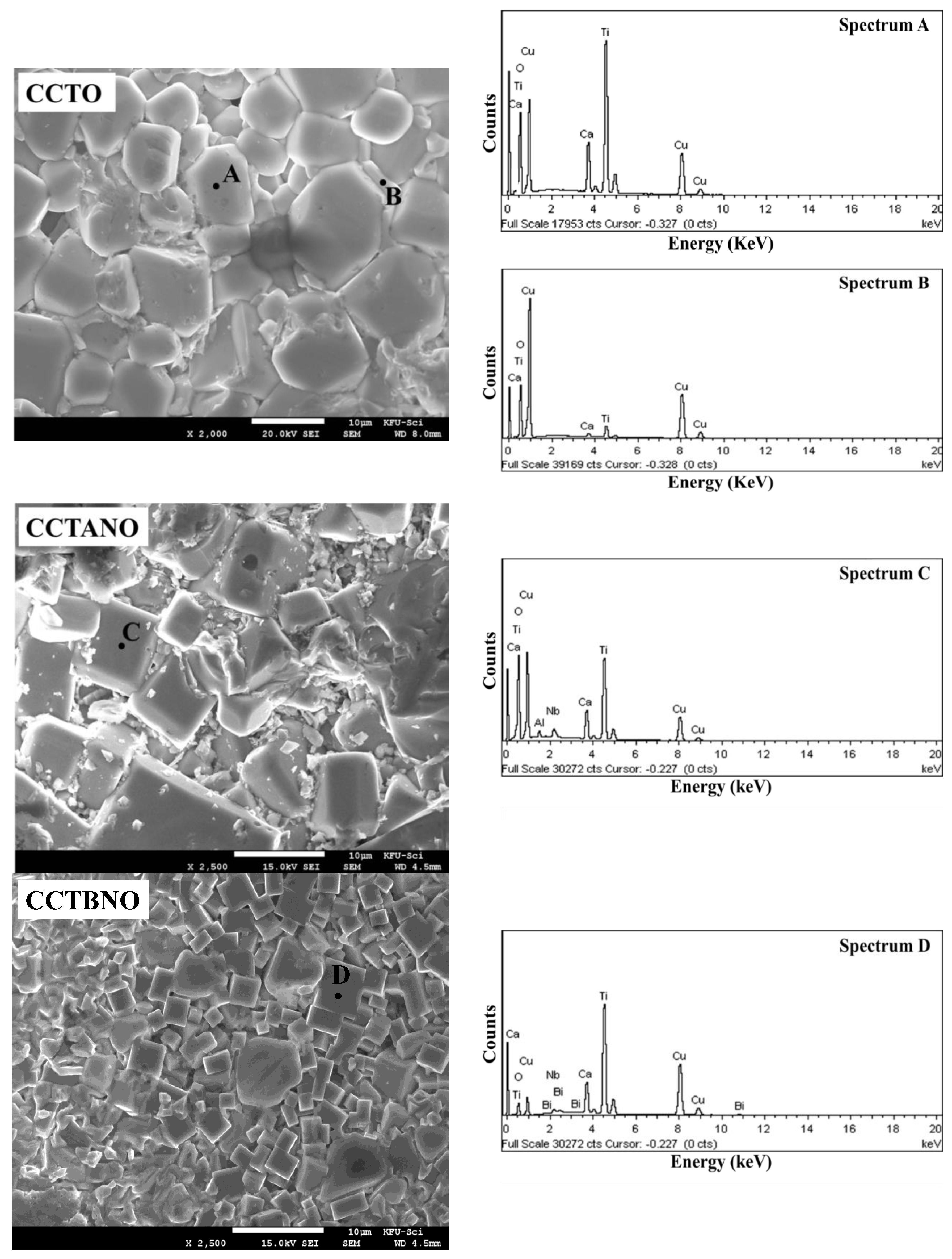
Figure 2 depicts the microstructure of CCTO, CCTANO, and CCTBNO ceramics as studied by FE-SEM. Similar grain size distribution was observed for CCTO (7–9 μm) and CCTANO (6–12 μm), while CCTBNO demonstrated a rather smaller but uniform grain size of ~3 μm. These grain-size values were clearly smaller than those in the literature for pure and cosubstituted CCTO ceramics prepared by a conventional solid state reaction (SSR) technique, which is in the 20–40 μm range [12,26,27]. The effect of doping on the grain size of CCTO ceramics was previously studied, where a reduction in the grain size of CCTO ceramics was observed that was attributed to the solute drag effect of the dopants [28,29]. Therefore, the smaller grain size of CCTBNO compared to that of other samples of the present study suggests that Bi dopants have more dragging force than that of Al.
Elemental analysis was carried out using energy dispersive X-ray (EDX) as shown in Figure 2. The elements of each composition were detected, and found to be uniformly distributed across grains and grain boundaries. Element-mole ratios obtained from EDX analysis of the grain were Ca:Cu:Ti = 1:2.87:3.97, Ca:Cu:Ti:Nb:Al = 1:3:3.68:0.16:0.17, and Ca:Cu:Ti:Nb:Bi = 1:3:3.68:0.17:0.13 for the CCTO, CCTANO, and CCTBNO ceramics, respectively. These results were close to the expected theoretical values based on the stoichiometry of each composition. Nevertheless, grains of the CCTO sample were found to be frequently surrounded by Cu-rich regions, as shown in Point B in Figure 2, where the element-mole ratio was found to be Ca:Cu:Ti = 1:42.91:3.92. These Cu-rich regions were probably due to the formation of a liquid CuO phase that wet the grains during sintering.
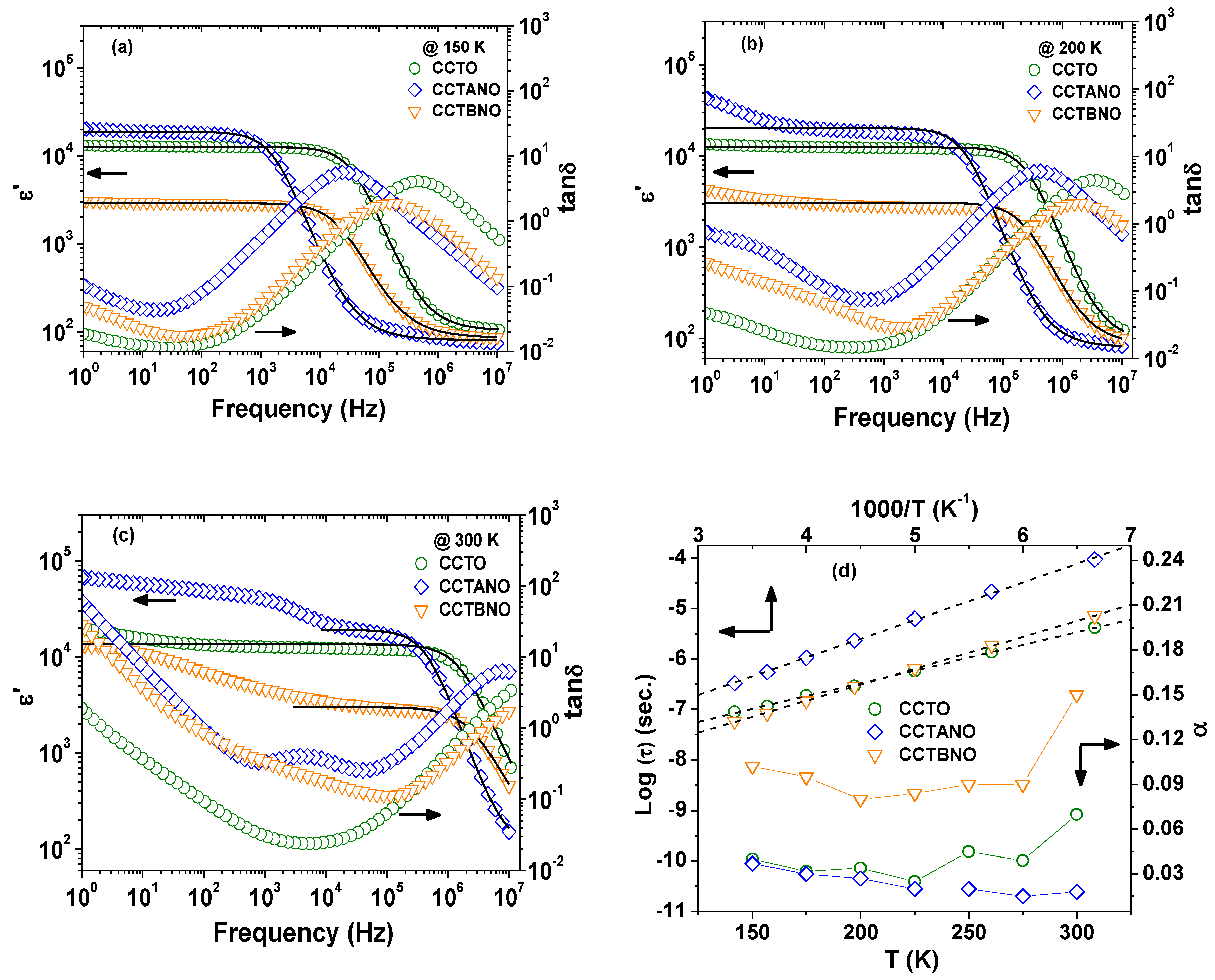
Figure 3a–c present the spectra of relative permittivity ε’ and dielectric loss tanδ at the selected temperatures of 150, 200, and 300 K. The frequency dependency of ε’ at 150 K for all samples showed one plateau followed by a steplike decrease in the high-frequency range, which is accompanied by a peak in the spectra of tanδ. With increasing temperature, ε’ increased, and the peak of tanδ shifted towards higher frequencies. This dielectric behavior was similar to a Debye-like relaxation process [4,30], which is generally related to the dipole relaxation in the system; however, it sometimes originates from the electrical heterogeneity of the system [31]. As shown by the solid lines in Figure 3a–c, the high-frequency relative permittivity spectra fit well with the modified Debye equation [32]:
where εs is static relative permittivity, ε∞ is the relative permittivity at high frequency, ω is angular frequency, τ is relaxation time, and α is a measure of the distribution of relaxation time (0 < α ≤ 1). For an ideal Debye relaxation, α = 1. Nevertheless, deviation from the modified Debye relaxation was observed for all ceramics at a low frequency, which denoted that there was an additional source of polarization responsible for the giant relative permittivity of the current ceramics. The temperature dependence of the extracted fitting parameters (τ and α) is given in Figure 3d. Values of α were found to be in the range of 0.02–0.15 for all samples, which indicated a distribution of relaxation time. Additionally, the temperature dependence of the fitted τ values was found to follow the Arrhenius law [33]:
where τ0 and ER are the pre-exponential factor and the activation energy for the relaxation, respectively. The calculated values of ER were 0.1, 0.125, and 0.147 eV for CCTO, CCTANO, and CCTBNO, respectively. These ER values were found to be similar to the relaxation energy in grain calculated from the analysis of modulus spectra of the samples, as is elaborated later in this section. Moreover, Figure 3 shows that pure CCTO displayed a superior dielectric property in terms of better ε’ stability and lower tanδ values over the studied frequency and temperature ranges. The CCTANO sample exhibited considerably superior ε’ values in the frequency range (1–106 Hz) at room temperature. The values of ε’ at 1 kHz and 300 K were 1.2 × 10⁴, 3.9 × 10⁴, and 4.6 × 10³ for the CCTO, CCTANO, and CCTBNO ceramics, respectively.
The values of minimal tanδ at room temperature were 0.023 (at 1 kHz), 0.255 (at 40 kHz), and 0.114 (at 115 kHz) for the CCTO, CCTANO, and CCTBNO ceramics, respectively. The dielectric performance of the CCTANO sample was comparable to that reported for CaCu3Ti4−x[(Al0.05Nb0.05)]xO12 (x:0–0.2) prepared by a high-temperature SSR method (ε’ = 2.9−4.1 × 10⁴, tanδ = 0.045–0.058 at 1 kHz) [12].
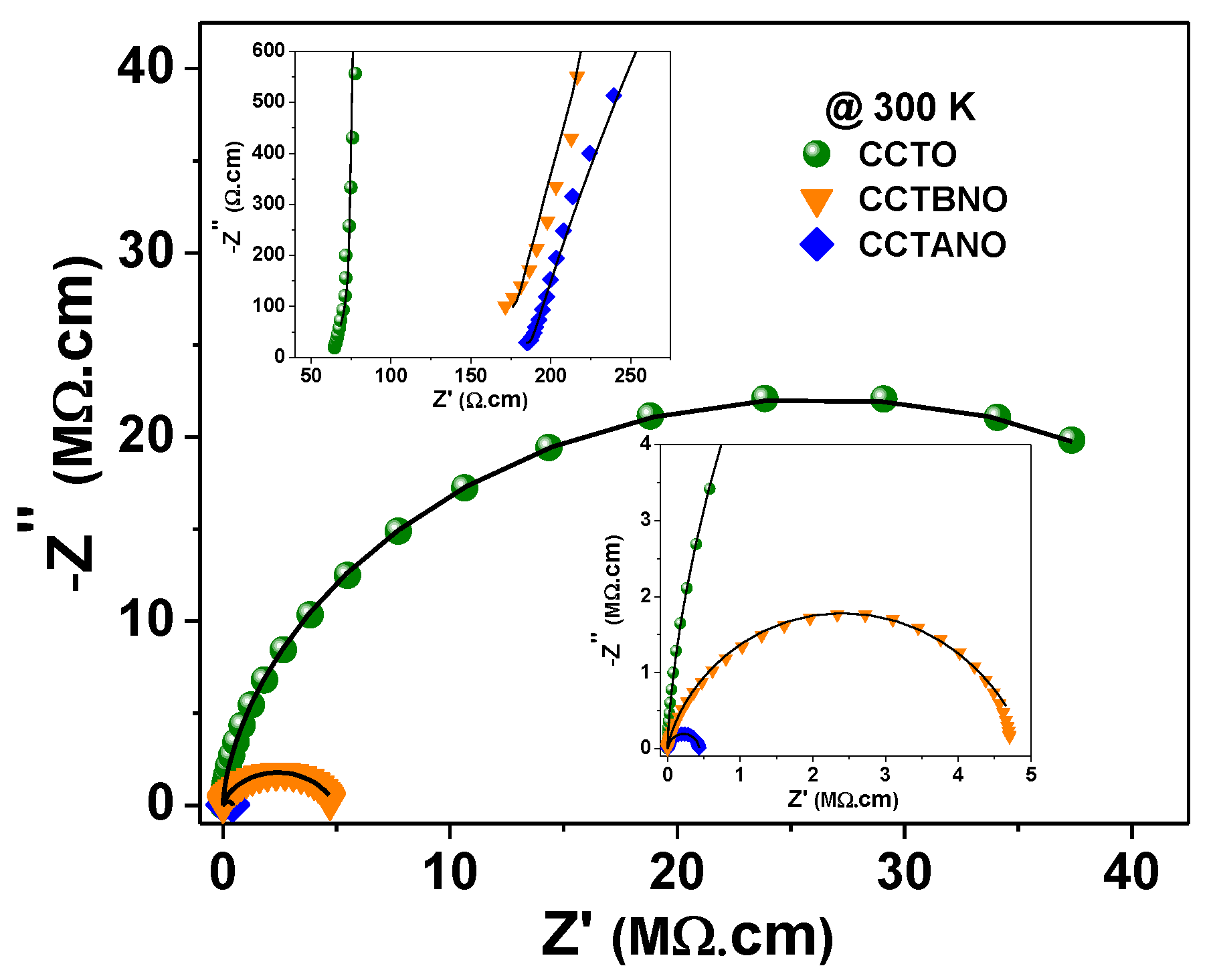
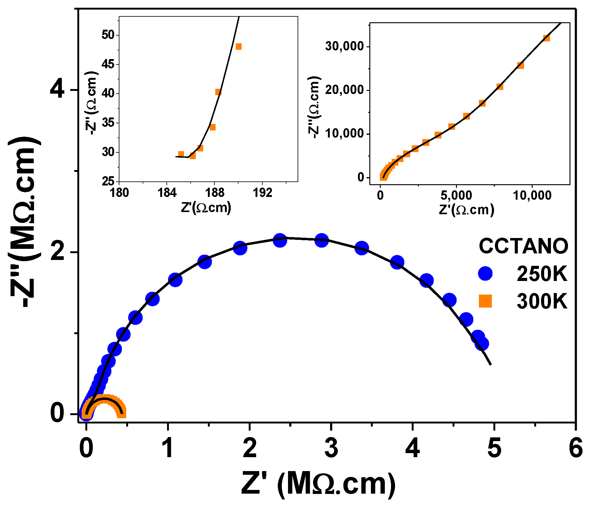
Figure 2 and Figure 3 show that CCTBNO had the lowest ε’ and smallest grain size. The CCTANO sample had a slightly larger grain size than that of CCTO, which correlated with the larger ε’ of the former. Therefore, the dielectric behavior of the CCTO, CCTANO, and CCTBNO ceramic samples tended to follow the IBLC model, where relative permittivity is correlated with grain size. Moreover, the lower dielectric performance of the CCTBNO ceramic was thought to be due to its lower CCTO-like phase content, as revealed by the Rietveld refinement analysis. Figure 4 shows the complex-impedance (Z*) plots at room temperature for the pure and cosubstituted CCTO ceramics of the current study. On the one hand, CCTO and CCTBNO samples showed similar features for Z* plot at room temperature, where a large semicircular arc that spread over a wide range of frequencies was observed. Nevertheless, the expanded view of the high-frequency region (see inset) shows a nonzero intercept of the impedance spectra. It is broadly accepted that the nonzero intercept at a high frequency is attributed to the grain response, whereas the large arc at a low frequency is assigned to the grain-boundary response [23]. Resistivity values for the grain and grain boundary, estimated from the intercept of the semicircular arcs with the Z’ axis, were found to be 70 and ~50 MΩ.cm for CCTO, and 187 and 4.7 MΩ.cm for CCTBNO. On the other hand, careful inspection of the Z* plot for CCTANO revealed the existence of three semicircular arcs at high, medium, and low frequencies, respectively, as shown in Figure 5 and the inserted expanded views. Thus, besides the grain response, additional contributions from grain boundaries and domain boundaries, and/or the electrode effect were possibly active in the CCTANO ceramics. The estimated resistivity values from the three arcs at room temperature were 187 Ω.cm (high frequency), 4.51 kΩ.cm (medium frequency), and 0.43 MΩ.cm (low frequency).
Moreover, Figure 4 and Figure 5 show that the semicircular arcs of the complex-impedance plots were depressed, which confirmed the nonideal Debye behavior as previously discussed in Figure 3. To model a nonideal Debye response, a constant phase element (CPE) is often used in the model equivalent circuit [34,35]. The capacitance value of the CPEi element is calculated using the following relation [36,37]:
where Ri, Qi, and ni are the CPEi’s fitting parameters, and n ranges from n = 0 for the purely resistant behavior to n = 1 for the purely capacitive behavior of the CPE element. Experimental complex-impedance data were well-fitted to the equivalent circuits shown in Table 2 using ZSimpWin (v3.10, Ametek, EChem software, Ann Arbor, MI, USA). In all cases, the chi2 value was in the order of 10−3–10−4, which reflects the goodness of fit as shown by the solid lines in Figure 4 and Figure 5. The obtained fitting parameters for the experimental data at 200 and 300 K are summarized in Table 2. The values of n were found to lie in the range of 0.91–0.98, indicating the close proximity of capacitance behavior. The estimated resistivity of the grain, grain boundary, and domain boundary (Rg) was close to their values calculated by the intercept method.
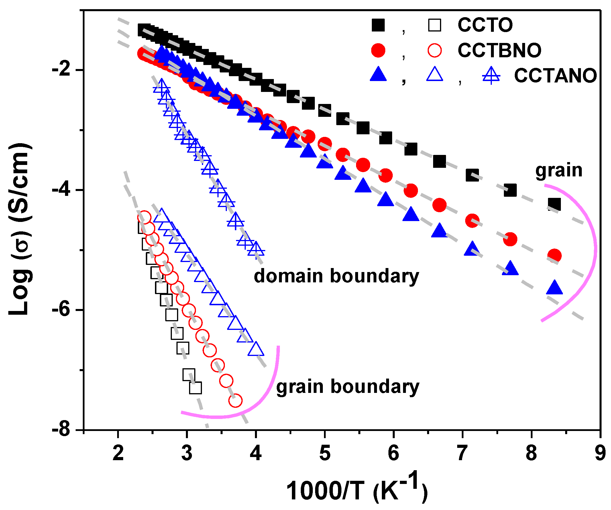
Thus, complex-impedance measurements of the current samples revealed their electrical inhomogeneity, where they were composed of semiconductor grains and electrically insulating regions in the form of domain and/or grain boundaries. This electrically inhomogeneous structure suggested the Maxwell–Wagner (M–W) polarization effect as the origin of the giant relative permittivity of the current samples, as shown in Figure 3. M–W polarization ascribes the effect of the polarization that takes place at blocking interfaces and boundaries such as sample surface/electrode, grain/grain boundary, and domain/domain boundary [4,5]. Figure 6 depicts the Arrhenius plots for the conductivity of the grain, domain-boundary, and grain-boundary regions. The activation-energy values for conduction could be calculated using the Arrhenius relation [33]:
where σ0 is the pre-exponential factor, kB is Boltzmann constant, and Ea is the activation energy for conduction. As summarized in Table 3, Ea values were close to the reported activation energy for the single- and doubly-ionized oxygen vacancies, which are typically in the 0.1–0.5 and 0.6–1.2 eV ranges, respectively [38]. Moreover, the value of the activation energy of grain conduction increases slightly by cosubstitution. In contrast, the value of Ea of grain-boundary conduction considerably decreases for cosubstituted ceramics.
Oxygen vacancies develop during a high-temperature (>1000 °C) sintering step due to oxygen loss [39]. Additional free electrons are expected by the partial substitution of Ti4+ by the pentavalent Nb5+, which explains the reduced resistivity of CCTANO and CCTBNO ceramics as compared to the pure CCTO sample. Moreover, the substitution of the Bi3+ acceptor ions for Ti4+ requires oxygen vacancies for charge conservation. Possible reaction equations, written using the Kröger–Vink notation for defects, are as follows:
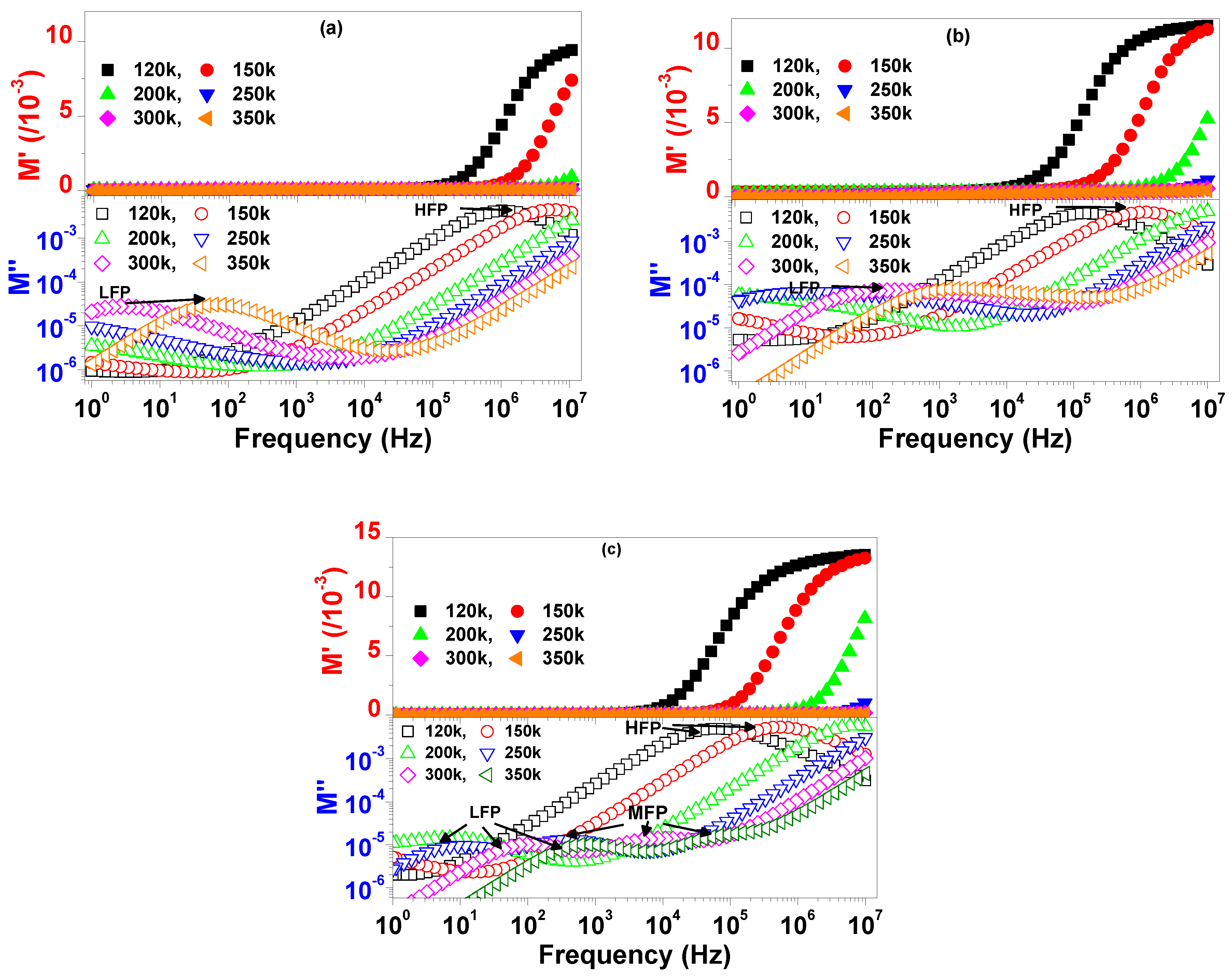
Considering the findings of complex-impedance measurements, the effect of Nb5+ dopants in reducing resistivity was more pronounced for grain boundaries, which explains the comparatively higher tanδ of the cosubstituted ceramics compared with that of CCTO. Moreover, free electrons might have been captured by Cu2+ and Ti4+, thus forming Cu+ and Ti3+ ions in order to maintain charge balance. Thus, the hopping of electrons between oxygen vacancies and mixed-valent structure of Cu+/Cu2+ and Ti3+/Ti4+ might have contributed to conduction in the present ceramics. Figure 7a–c show the spectra of the real (M’) and imaginary (M’’) parts of the electric modulus at selected temperatures of 120, 150, 200, 250, 300, and 350 K. M’ values were nearly zero at low frequencies for all samples and increased with frequency, which indicated the suppression of electrode polarization effects [40]. Two relaxation peaks could be seen in the spectrum of M’’ for CCTO and CCTBNO. At low temperatures, the first peak appeared at a high frequency (HFP); then, with increasing temperature, a second peak began at low frequencies (LFP). Both peaks were thermally activated, where they shifted towards higher frequencies with increasing temperature. The existence of high- and low-frequency peaks is commonly reported for CCTO-based ceramics, and is attributed to the response of the grain and grain boundary, respectively [12,30].
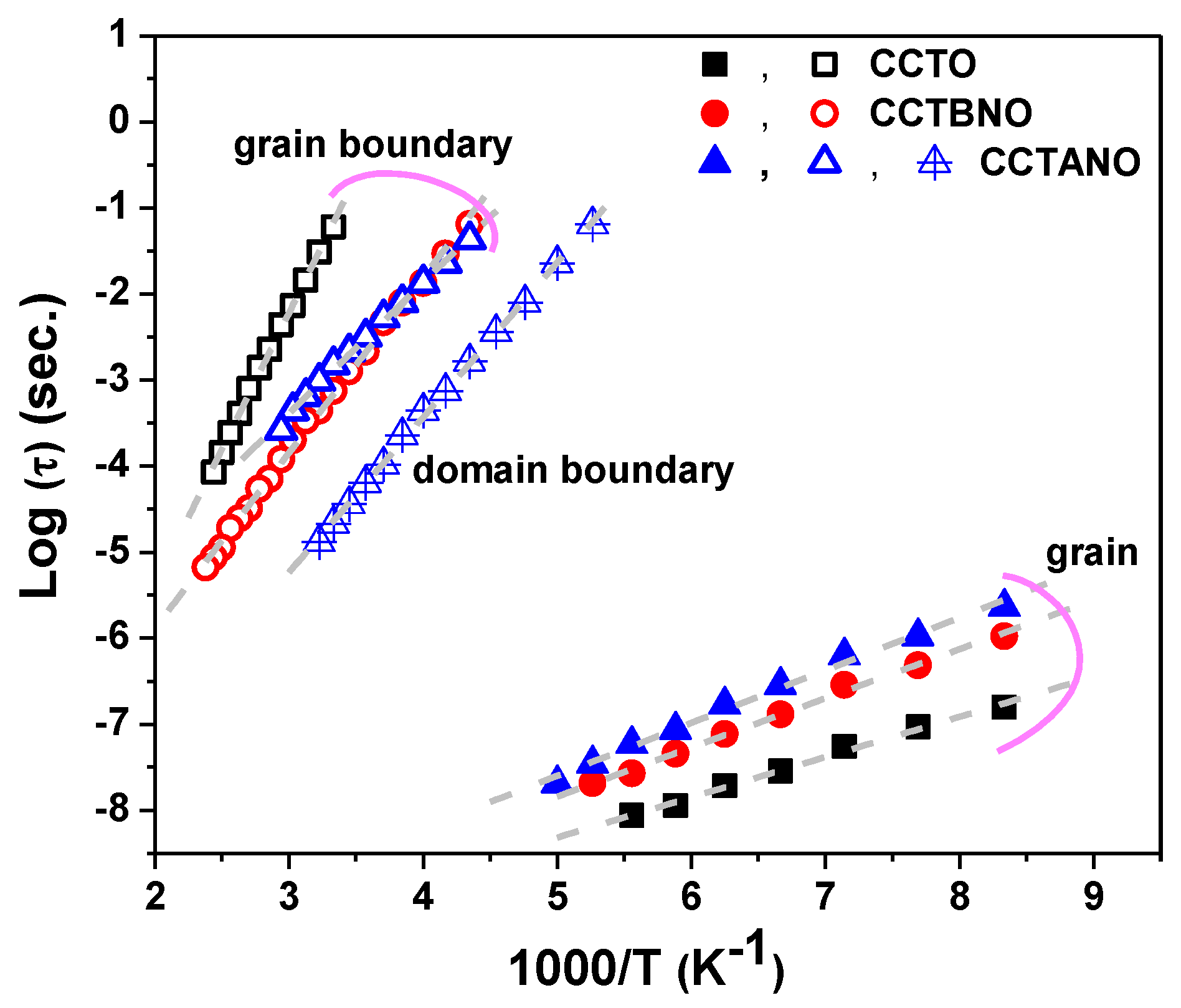
As depicted in Figure 7c, three thermally activated peaks existed in the spectra of M’’ for the CCTANO sample. In addition to the commonly reported low- and high-frequency peaks, a third peak appeared at medium frequencies (MFP). The frequency at the peak maximum of the M’’ spectra (fmax) was related to relaxation time (τ) as τ = 1/2πfmax. As shown in Figure 8, temperature dependency of τ follows the Arrhenius law (Equation (3)). Calculated ER values related to the different relaxation peaks are given in Table 3. ER values were close to the Ea values, and both were in the reported range of activation energies of oxygen vacancies, as previously discussed. Thus, the single- and doubly-ionized oxygen vacancies played a considerable role in the relaxation and conduction responses of the investigated samples.
4. Conclusions
CaCu3Ti4-x[(A0.05Nb0.05)]xO12 ceramics (A: Al and Bi; x = 0, 0.3) were synthesized by high-energy mechanical ball milling and reactive sintering inside a tubular furnace for 15 h at 1050 °C in air. X-ray diffraction measurements revealed a cubic CCTO structure as the main phase for all ceramic samples. Nevertheless, the (Bi3+, Nb5+)-cosubstituted CCTO demonstrated a secondary pyrochlore phase content of ~18% (mole ratio). It also showed the smallest and most uniform grain size of ~3 μm compared to the pure (7–9 μm) and (Al3+, Nb5+)-cosubstituted CCTO (6–12 μm). The studied ceramics showed colossal relative permittivity (ε’ > 103) over wide ranges of temperature and frequency, with the (Al3+, Nb5+)-cosubstituted CCTO sample having the highest relative permittivity of ε’ = 3.9 × 10⁴ at 1 kHz and 300 K. The giant relative permittivity of the ceramics could be attributed to the Maxwell–Wagner polarization effect at the blocking grain and domain boundaries. Meanwhile, cosubstituted CCTO samples of the present study revealed degradation of its dielectric loss (tanδ), which was attributed to the decrease in grain-boundary resistance, as revealed by impedance-spectroscopy analysis. Modulus-spectrum analysis revealed two relaxation processes for the pure and (Bi3+, Nb5+)-cosubstituted CCTO samples. Dissimilar behavior was observed for (Al3+, Nb5+)-cosubstituted CCTO, where three relaxation mechanisms contributed and were attributed for the grain, domain-boundary, and grain-boundary responses. The calculated activation energies highlighted the role of single- and doubly-ionized oxygen vacancies in the relaxation and conduction responses of the investigated samples.
Author Contributions
Conceptualization, H.M.K.; formal analysis, H.M.K., M.M.A., and K.Y.; funding acquisition, A.A.; investigation, H.M.K. and A.A.; project administration, M.M.A.; software, K.Y.; validation, M.M.A.; writing—original draft, H.M.K. and M.M.A.; writing—review and editing, A.A. All authors have read and agreed to the published version of the manuscript.
Funding
This research was funded by the Deanship of Scientific Research in King Faisal University (Saudi Arabia; grant number 17122003. The APC was funded by the same grant).
Acknowledgments
The authors acknowledge the Deanship of Scientific Research at King Faisal University (Saudi Arabia) for the financial support under the Research Group Support Track (grant no. 17122003).
Conflicts of Interest
The authors declare no conflict of interest.
References
- Subramanian, M.A.; Li, D.; Duan, N.; Reisner, B.A.; Sleight, A.W. High Relative Permittivity in ACu3Ti4O12 and ACu3Ti3FeO12 Phases. J. Solid State Chem. 2000, 151, 323–325. [Google Scholar] [CrossRef]
- Chung, S.-Y.; Kim, I.-D.; Kang, S.-J.L. Strong Nonlinear Current—Voltage Behaviour in Perovskite-Derivative Calcium Copper Titanate. Nat. Mater. 2004, 3, 774–778. [Google Scholar] [CrossRef]
- Li, M.; Shen, Z.J.; Nygren, M.; Feteira, A.; Sinclair, D.C.; West, A.R. Origin(s) of the Apparent High Permittivity in CaCu3Ti4O12 Ceramics: Clarification on the Contributions from Internal Barrier Layer Capacitor and Sample-Electrode Contact Effects. J. Appl. Phys. 2009, 106, 104106. [Google Scholar] [CrossRef]
- Liu, J.; Duan, C.-G.; Yin, W.-G.; Mei, W.N.; Smith, R.W.; Hardy, J.R. Large dielectric constant and Maxwell-Wagner relaxation in Bi2/3Cu3Ti4O12. Phys. Rev. B 2004, 70, 144106. [Google Scholar] [CrossRef]
- Priya, A.S.; Geetha, D.; Kavitha, N. Effect of Al Substitution on the Structural, Electric and Impedance Behavior of Cobalt Ferrite. Vacuum 2019, 160, 453–460. [Google Scholar] [CrossRef]
- Liu, P.; Lai, Y.; Zeng, Y.; Wu, S.; Huang, Z.; Han, J. Influence of Sintering Conditions on Microstructure and Electrical Properties of CaCu3Ti4O12 (CCTO) Ceramics. J. Alloy. Compd. 2015, 650, 59–64. [Google Scholar] [CrossRef]
- Zheng, H.F.Q.; Fan, H. Influence of Fabrication Parameters on the Phase Formation and Dielectric Properties of CaCu3Ti4O12 Ceramics. J. Mater. Sci. Technol. 2012, 28, 920–926. [Google Scholar] [CrossRef]
- Huang, Y.; Shi, D.; Li, Y.; Li, G.; Wang, Q.; Liu, L.; Fang, L. Effect of Holding Time on the Dielectric Properties and Non-Ohmic Behavior of CaCu3Ti4O12 Capacitor-Varistors. J. Mater. Sci. Mater. Electron. 2012, 24, 1994–1999. [Google Scholar] [CrossRef]
- Kumar, R.; Zulfequar, M.; Sharma, L.; Singh, V.N.; Senguttuvan, T.D. Growth of Anocrystalline CaCu3Ti4O12 Ceramic by the Microwave Flash Combustion Method: Structural and Impedance Spectroscopic Studies. Cryst. Growth Des. 2015, 15, 1374–1379. [Google Scholar] [CrossRef]
- Lin, H.; He, X.; Gong, Y.; Pang, D.; Yi, Z. Tuning the Nonlinear Current-Voltage Behavior of CaCu3Ti4O12 Ceramics by Spark Plasma Sintering. Ceram. Int. 2018, 44, 8650–8655. [Google Scholar]
- Espinoza-González, R.; Hevia, S.; Adrian, A. Effects of Strontium/Lanthanum Co-doping on the Dielectric Properties of CaCu3Ti4O12 Prepared by Reactive Sintering. Ceram. Int. 2018, 44, 15588–15595. [Google Scholar] [CrossRef]
- Boonlakhorn, J.; Kidkhunthod, P.; Chanlek, N.; Thongbai, P. (Al3+, Nb5+) Co–doped CaCu3Ti4O12: An Extended Approach for Acceptor-Donor Heteroatomic Substitutions to Achieve High-Performance Giant-Dielectric Permittivity. J. Eur. Ceram. Soc. 2018, 38, 137–143. [Google Scholar] [CrossRef]
- Mahfoz Kotb, H.; Ahmad, M.M. Electrical and Dielectric Properties of Na1/2La1/2Cu3Ti4O12 Ceramics Prepared by High Energy Ball-Milling and Conventional Sintering. Chin. Phys. B 2016, 25, 128201. [Google Scholar] [CrossRef]
- Mahfoz Kotb, H.; Ahmad, M.M.; Aldabal, S.; Alshoaibi, A.; Aljaafari, A. Structural and Dielectric Behavior of Al-Substituted CaCu3Ti4O12 Ceramics with Giant Relative Permittivity by Spark Plasma Sintering. J. Mater. Sci. Mater. Electron. 2019, 30, 18259–18267. [Google Scholar] [CrossRef]
- Mahfoz Kotb, H. Electrical and Dielectric Properties of NSCTO. Chin. Phys. B 2019, 28, 098202. [Google Scholar] [CrossRef]
- Ahmad, M.M. Giant Relative Permittivity in CaCu3Ti4O12 Nanoceramics. Appl. Phys. Lett. 2013, 102, 232908. [Google Scholar] [CrossRef]
- Thomazini, D.; Gelfuso, M.V.; Volpi, G.M.S.; Eiras, J.A. Conventional and Microwave-Assisted Sintering of CaCu3Ti4O12 Ceramics Obtained from Coprecipitated Powders. Int. J. Appl. Ceram. Technol. 2015, 12, E73–E81. [Google Scholar] [CrossRef]
- Song, Y.; Liu, P.; Guo, B.; Cui, X.; Yang, W. Giant Permittivity Up to 100 MHz in La and Nb Co-doped Rutile TiO2 Ceramics. J. Am. Ceram. Soc. 2020, 103, 4313–4320. [Google Scholar] [CrossRef]
- Wang, X.; Zhang, B.; Shen, G.; Sun, L.; Hu, Y.; Shi, L.; Wang, X.; Jie, C.; Zhang, L. Colossal Permittivity and Impedance Analysis of Tantalum and Samarium Co-doped TiO2 Ceramics. Ceram. Int. 2017, 43, 13349–13355. [Google Scholar] [CrossRef]
- Boonlakhorn, J.; Srepusharawoot, P.; Thongbai, P. Distinct Roles between Complex Defect Clusters and Insulating Grain Boundary on Dielectric Loss Behaviors of (In3+/Ta5+) Co-doped CaCu3Ti4O12 Ceramics. Results Phys. 2020, 16, 102886. [Google Scholar] [CrossRef]
- Wen, A.; Zhang, Y.; Zhu, J.; Yuan, D. Study on the Semiconducting Grain and Insulating Barrier Layer in Aluminum/Niobium Co-doped CCTO. In Physics and Techniques of Ceramic and Polymeric Materials, Proceedings of the Chinese Materials Conference (CMC 2018), Xiamen, China, 12–16 July 2018; Han, Y., Ed.; Springer: Singapore, 2019; Volume 216, pp. 195–203. [Google Scholar]
- Hu, W.; Liu, Y.; Withers, R.L.; Frankcombe, T.J.; Norén, L.; Snashall, A.; Kitchin, M.; Smith, P.; Gong, B.; Chen, H.; et al. Electron-Pinned Defect-Dipoles for High-Performance Colossal Permittivity Materials. Nat. Mater. 2013, 12, 821–826. [Google Scholar] [CrossRef]
- Adams, T.B.; Sinclair, D.C.; West, A.R. Characterization of Grain Boundary Impedances in Fine- and Coarse-Grained CaCu3Ti4O12 Ceramics. Phys. Rev. B 2006, 73. [Google Scholar] [CrossRef]
- Cao, G.; Feng, L.; Wang, C. Grain-Boundary and Subgrain-Boundary Effects on the Dielectric Properties of CaCu3Ti4O12 Ceramics. J. Phys. D Appl. Phys. 2007, 40, 2899–2905. [Google Scholar] [CrossRef]
- Izumi, F.; Ikeda, T. A Rietveld-Analysis Programm RIETAN-98 and Its Applications to Zeolites. Mater. Sci. Forum 2000, 321-324, 198–205. [Google Scholar] [CrossRef]
- Somphan, W.; Sangwong, N.; Yamwong, T.; Thongbai, P. Giant Dielectric and Electrical Properties of Sodium Yttrium Copper Titanate: Na1/2Y1/2Cu3Ti4O12. J. Mater. Sci. Mater. Electron. 2011, 23, 1229–1234. [Google Scholar] [CrossRef]
- Liang, P.; Li, Y.; Zhao, Y.; Wei, L.; Yang, Z. Origin of Giant Permittivity and High-Temperature Dielectric Anomaly Behavior in Na0.5Y0.5Cu3Ti4O12 Ceramics. J. Appl. Phys. 2013, 113, 224102. [Google Scholar] [CrossRef]
- Thongbai, P.; Putasaeng, B.; Yamwong, T.; Maensiri, S. Modified Giant Dielectric Properties of Samarium Doped CaCu3Ti4O12 Ceramics. Mater. Res. Bull. 2012, 47, 2257–2263. [Google Scholar] [CrossRef]
- Boonlakhorn, J.; Thongbai, P.; Putasaeng, B.; Yamwong, T.; Maensiri, S. Very High-Performance Dielectric Properties of Ca1−3x/2YbxCu3Ti4O12 Ceramics. J. Alloy. Compd. 2014, 612, 103–109. [Google Scholar] [CrossRef]
- Peng, Z.; Zhou, X.; Wang, J.; Zhu, J.; Liang, P.; Chao, X.; Yang, Z. Origin of Colossal Permittivity and Low Dielectric Loss in Na1/3Cd1/3Y1/3Cu3Ti4O12 Ceramics. Ceram. Int. 2020, 46, 11154–11159. [Google Scholar] [CrossRef]
- Liu, J.; Duan, C.-G.; Mei, W.N.; Smith, R.W.; Hardy, J.R. Dielectric Properties and Maxwell-Wagner Relaxation of Compounds ACuTiO (A=Ca, Bi2/3, Y2/3, La2/3). J. Appl. Phys. 2005, 98, 093703. [Google Scholar] [CrossRef]
- Asami, K. Characterization of Heterogeneous Systems by Dielectric Spectroscopy. Prog. Polym. Sci. 2002, 27, 1617–1659. [Google Scholar] [CrossRef]
- Nobre, M.A.L.; Lanfredi, S. Grain Boundary Electric Characterization of Zn7Sb2O12 Semiconducting Ceramic: A Negative Temperature Coefficient Thermistor. J. Appl. Phys. 2003, 93, 5576. [Google Scholar] [CrossRef] [Green Version]
- Abram, E.; Sinclair, D.; West, A.R. A Strategy for Analysis and Modelling of Impedance Spectroscopy Data of Electroceramics: Doped Lanthanum Gallate. J. Electroceramics 2003, 10, 165–177. [Google Scholar] [CrossRef]
- Khopkar, V.; Sahoo, B. Low Temperature Dielectric Properties and NTCR Behavior of the BaFe0.5Nb0.5O3 Double Perovskite Ceramic. Phys. Chem. Chem. Phys. 2020, 22, 2986–2998. [Google Scholar]
- Fleig, J. The Grain Boundary Impedance of Random Microstructures Numerical Simulations and Implications. Solid State Ion. 2002, 150, 181–193. [Google Scholar] [CrossRef]
- Bieberlehutter, A.; Sogaard, M.; Tuller, H.L. Electrical and Electrochemical Characterization of Microstructured Thin Film La1−xSrxCoO3 Electrodes. Solid State Ion. 2006, 177, 1969–1975. [Google Scholar] [CrossRef]
- Li, J.; Liang, P.; Yi, J.; Chao, X.; Yang, Z.; Wong-Ng, W.K. Phase Formation and Enhanced Dielectric Response of Y2/3Cu3Ti4O12Ceramics Derived from the Sol-Gel Process. J. Am. Ceram. Soc. 2015, 98, 795–803. [Google Scholar] [CrossRef]
- Sinclair, D.C.; Adams, T.B.; Morrison, F.D.; West, A.R. CaCu3Ti4O12: One-Step Internal Barrier Layer Capacitor. Appl. Phys. Lett. 2002, 80, 2153–2155. [Google Scholar] [CrossRef]
- Liang, P.; Chao, X.; Wang, F.; Liu, Z.; Yang, Z.; Alford, N. The Lowered Dielectric Loss and Grain-Boundary Effects in La-doped Y2/3Cu3Ti4O12 Ceramics. J. Am. Ceram. Soc. 2013, 96, 3883–3890. [Google Scholar] [CrossRef]
Figure 1.
Rietveld refinements of XRD patterns of (a) CaCu3Ti4O12 (CCTO), (b) CCTANO, and (c) CCTBNO ceramics. Yobs, experimental data; Ycal, calculated data. The symbol (?) represents an unindexed peak.
Figure 1.
Rietveld refinements of XRD patterns of (a) CaCu3Ti4O12 (CCTO), (b) CCTANO, and (c) CCTBNO ceramics. Yobs, experimental data; Ycal, calculated data. The symbol (?) represents an unindexed peak.


Figure 2.
(left) FE-SEM micrographs for fractured surface of CCTO, CCTANO, and CCTBNO ceramic samples; (right) EDX spectrum for marked points.
Figure 2.
(left) FE-SEM micrographs for fractured surface of CCTO, CCTANO, and CCTBNO ceramic samples; (right) EDX spectrum for marked points.

Figure 3.
Spectra of ε’ and tanδ for CCTO, CCTANO, and CCTBNO ceramics at (a) 150, (b) 200, and (c) 300 K; (d) temperature dependence of τ and α. Solid and dashed lines, fitting results by modified Debye equation and Arrhenius relation, respectively.
Figure 3.
Spectra of ε’ and tanδ for CCTO, CCTANO, and CCTBNO ceramics at (a) 150, (b) 200, and (c) 300 K; (d) temperature dependence of τ and α. Solid and dashed lines, fitting results by modified Debye equation and Arrhenius relation, respectively.

Figure 4.
Room-temperature complex-impedance plan (Z*) plots for CCTO, CCTBNO, and CCTANO ceramics. Solid lines, fitting of measured data to equivalent circuits (Table 2).
Figure 4.
Room-temperature complex-impedance plan (Z*) plots for CCTO, CCTBNO, and CCTANO ceramics. Solid lines, fitting of measured data to equivalent circuits (Table 2).

Figure 5.
Complex-impedance plan (Z*) plots for CCTO, CCTANO, and CCTBNO ceramics at selected temperatures. Solid lines, fitting of measured data to equivalent circuit (Table 2).
Figure 5.
Complex-impedance plan (Z*) plots for CCTO, CCTANO, and CCTBNO ceramics at selected temperatures. Solid lines, fitting of measured data to equivalent circuit (Table 2).

Figure 6.
Arrhenius plots of conductivity for CCTO, CCTBNO, and CCTANO ceramics.

Figure 7.
Spectra of M’ and M’’ for (a) CCTO, (b) CCTBNO, and (c) CCTANO ceramics at selected temperatures.
Figure 7.
Spectra of M’ and M’’ for (a) CCTO, (b) CCTBNO, and (c) CCTANO ceramics at selected temperatures.

Figure 8.
Arrhenius plots of relaxation time for CCTO, CCTANO, and CCTBNO ceramics.


Table 1.
Lattice parameter (a), unit cell volume (V) for main CCTO phase, and agreement factors of profile (Rp), weighted profile (Rwp), structure (RF), and goodness of fit (GofF) obtained through Rietveld refinement.
Table 1.
Lattice parameter (a), unit cell volume (V) for main CCTO phase, and agreement factors of profile (Rp), weighted profile (Rwp), structure (RF), and goodness of fit (GofF) obtained through Rietveld refinement.
| Sample | CCTO | CCTANO | CCTBNO |
|---|---|---|---|
| Space group | Im3 | Im3 | Im3 |
| a (Å) | 7.394 (3) | 7.397 (8) | 7.40056 |
| V (Å3) | 404.28 (1) | 404.86 (1) | 405.3165 |
| Rp (%) | 11.820 | 16.316 | 11.256 |
| Rwp (%) | 15.552 | 21.429 | 15.357 |
| RB (%) | 10.453 | 13.805 | 7.741 |
| RF (%) | 8.582 | 12.305 | 5.675 |
| GofF | 1.74 | 2.22 | 2.0 |
Table 2.
Values of equivalent-circuit parameters at selected temperatures by ZSimpWin fitting.
| Sample | Temperature/Equivalent Circuit | R1-grain Ω.cm | CPE1 | R2-g.b. Ω.cm | CPE2 | R3-d.b. Ω.cm | CPE3 | |||
|---|---|---|---|---|---|---|---|---|---|---|
| C1 (nF) | n1 | C2 (nF) | n | C3 (nF) | n3 | |||||
| CCTO | 200 K  | 470 | 0.016 | 0.99 | 3.4 × 10⁹ | 2.6 | 0.98 | - | - | - |
300 K  | 63 | - | - | 48 × 106 | 31.3 | 0.92 | - | - | - | |
| CCTBNO | 200 K  | 573 | 0.029 | 0.99 | 3.8 × 10⁸ | 1.3 | 0.96 | - | - | - |
300 K  | 191 | - | - | 4.3 × 10⁶ | 1.1 | 0.91 | - | - | - | |
| CCTANO | 200 K  | 3592 | 0.024 | 0.93 | 24 × 107 | 13.6 | 0.98 | 2 × 10⁶ | 10 | 0.96 |
300 K  | 189 | - | - | 1.4 × 10⁵ | 6.1 | 0.93 | 1.8 × 10³ | 13 | 0.95 | |
Table 3.
Activation energy for conduction Ea (eV) and relaxation ER (eV).
| Sample | Ea(g.) | Ea(d.b.) | Ea(g.b.) | ER(PHF) | ER(PMF) | ER(PLF) |
|---|---|---|---|---|---|---|
| CCTO | 0.093 | - | 0.628 | 0.099 | - | 0.751 |
| CCTBNO | 0.113 | - | 0.404 | 0.114 | - | 0.444 |
| CCTANO | 0.121 | 0.357 | 0.301 | 0.131 | 0.390 | 0.327 |
Publisher’s Note: MDPI stays neutral with regard to jurisdictional claims in published maps and institutional affiliations. |
© 2020 by the authors. Licensee MDPI, Basel, Switzerland. This article is an open access article distributed under the terms and conditions of the Creative Commons Attribution (CC BY) license (http://creativecommons.org/licenses/by/4.0/).
Share and Cite
MDPI and ACS Style
Kotb, H.M.; Ahmad, M.M.; Alshoaibi, A.; Yamada, K. Dielectric Response and Structural Analysis of (A3+, Nb5+) Cosubstituted CaCu3Ti4O12 Ceramics (A: Al and Bi). Materials 2020, 13, 5822. https://0-doi-org.brum.beds.ac.uk/10.3390/ma13245822
AMA Style
Kotb HM, Ahmad MM, Alshoaibi A, Yamada K. Dielectric Response and Structural Analysis of (A3+, Nb5+) Cosubstituted CaCu3Ti4O12 Ceramics (A: Al and Bi). Materials. 2020; 13(24):5822. https://0-doi-org.brum.beds.ac.uk/10.3390/ma13245822
Chicago/Turabian StyleKotb, Hicham Mahfoz, Mohamad M. Ahmad, Adil Alshoaibi, and Koji Yamada. 2020. "Dielectric Response and Structural Analysis of (A3+, Nb5+) Cosubstituted CaCu3Ti4O12 Ceramics (A: Al and Bi)" Materials 13, no. 24: 5822. https://0-doi-org.brum.beds.ac.uk/10.3390/ma13245822
Note that from the first issue of 2016, this journal uses article numbers instead of page numbers. See further details here.