
Physical and Geometrical Properties of Additively Manufactured Pure Copper Samples Using a Green Laser Source


Abstract
:1. Introduction
2. Experimental Setup
2.1. Powder
2.2. Machine
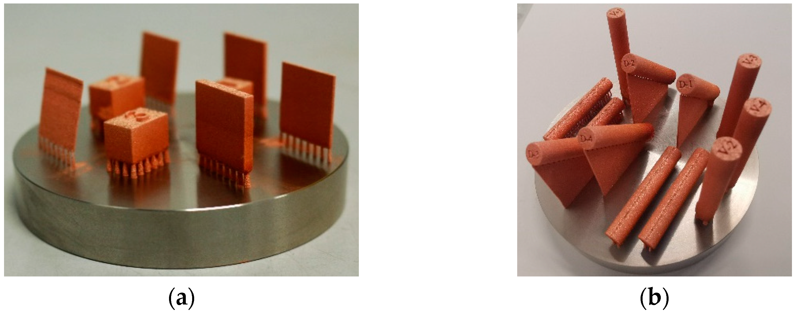
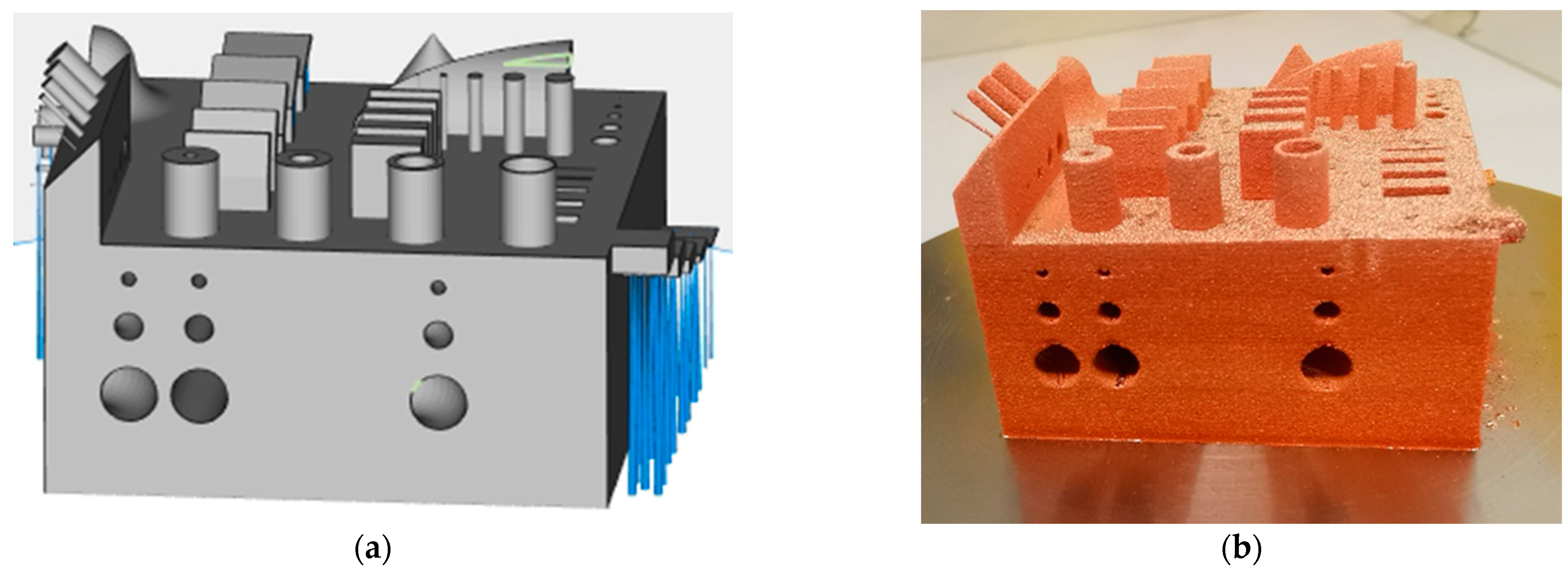
2.3. Samples
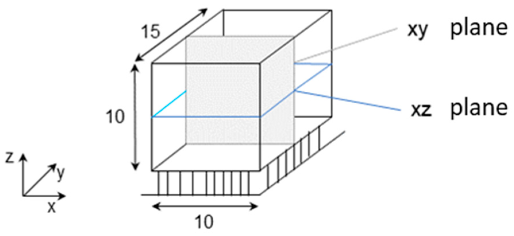
2.4. Sample Preparation
2.5. Conductivity Measurement
3. Results and Discussion
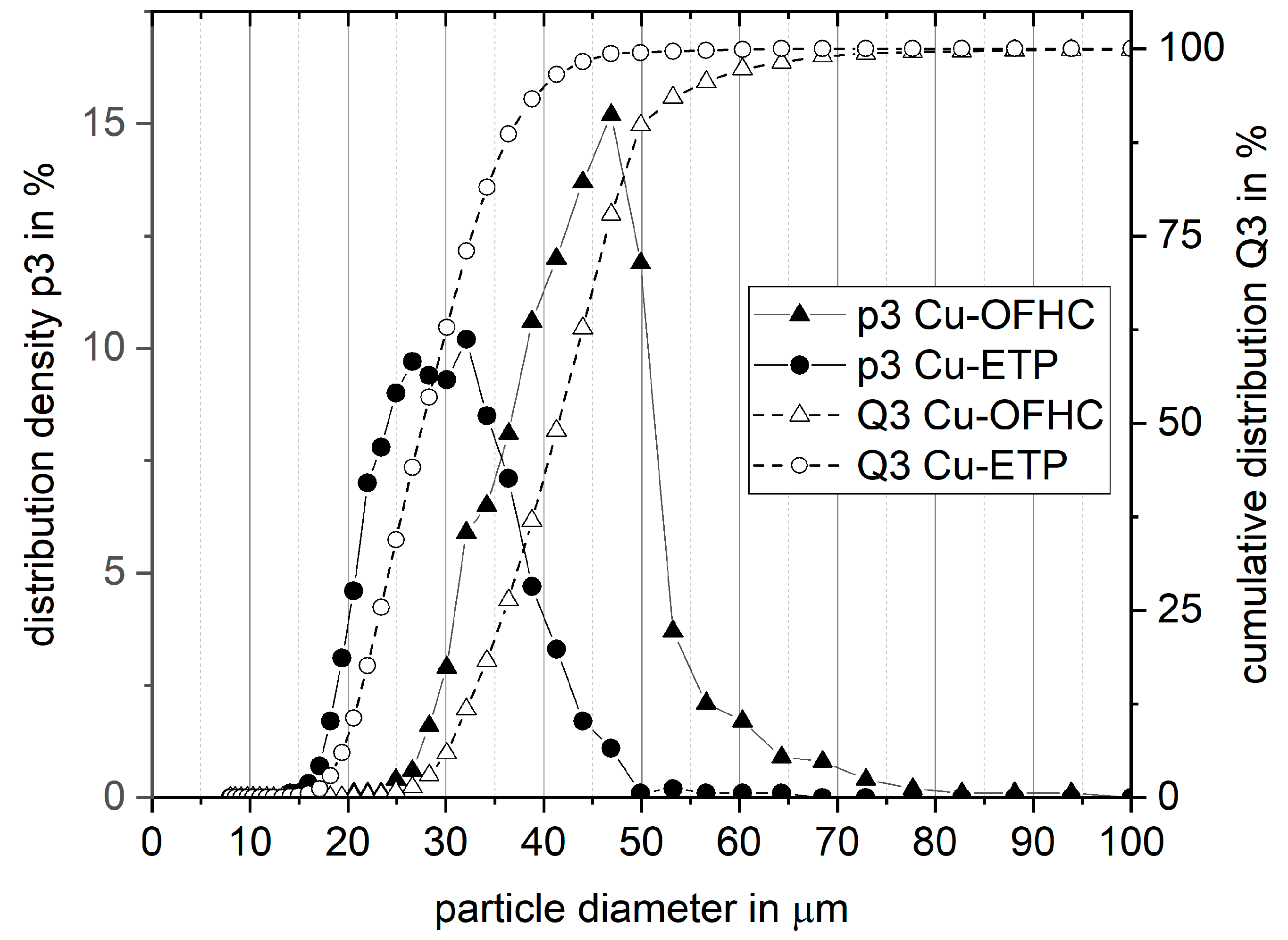
3.1. Powder Analysis
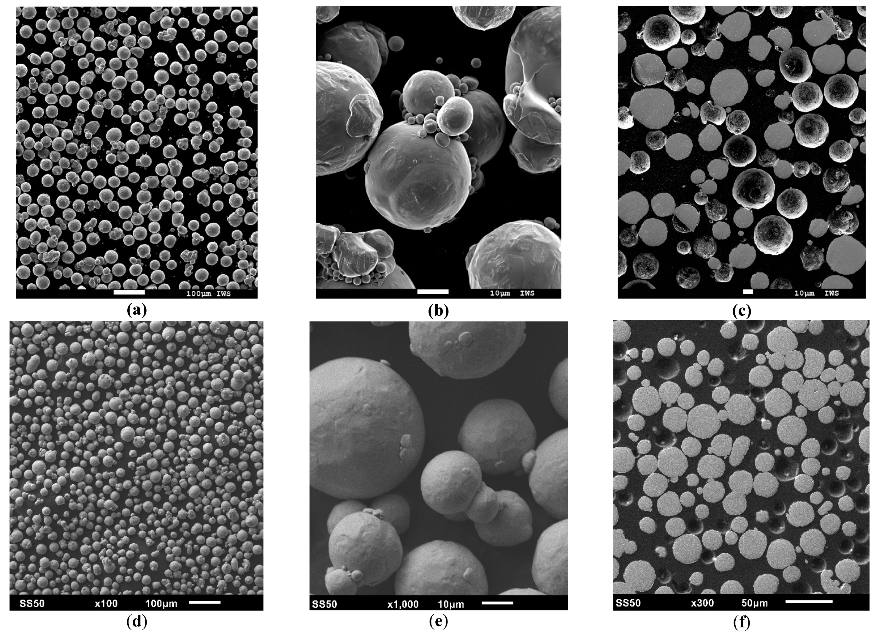
3.1.1. Morphology
3.1.2. Chemical Composition
3.1.3. Absorptivity
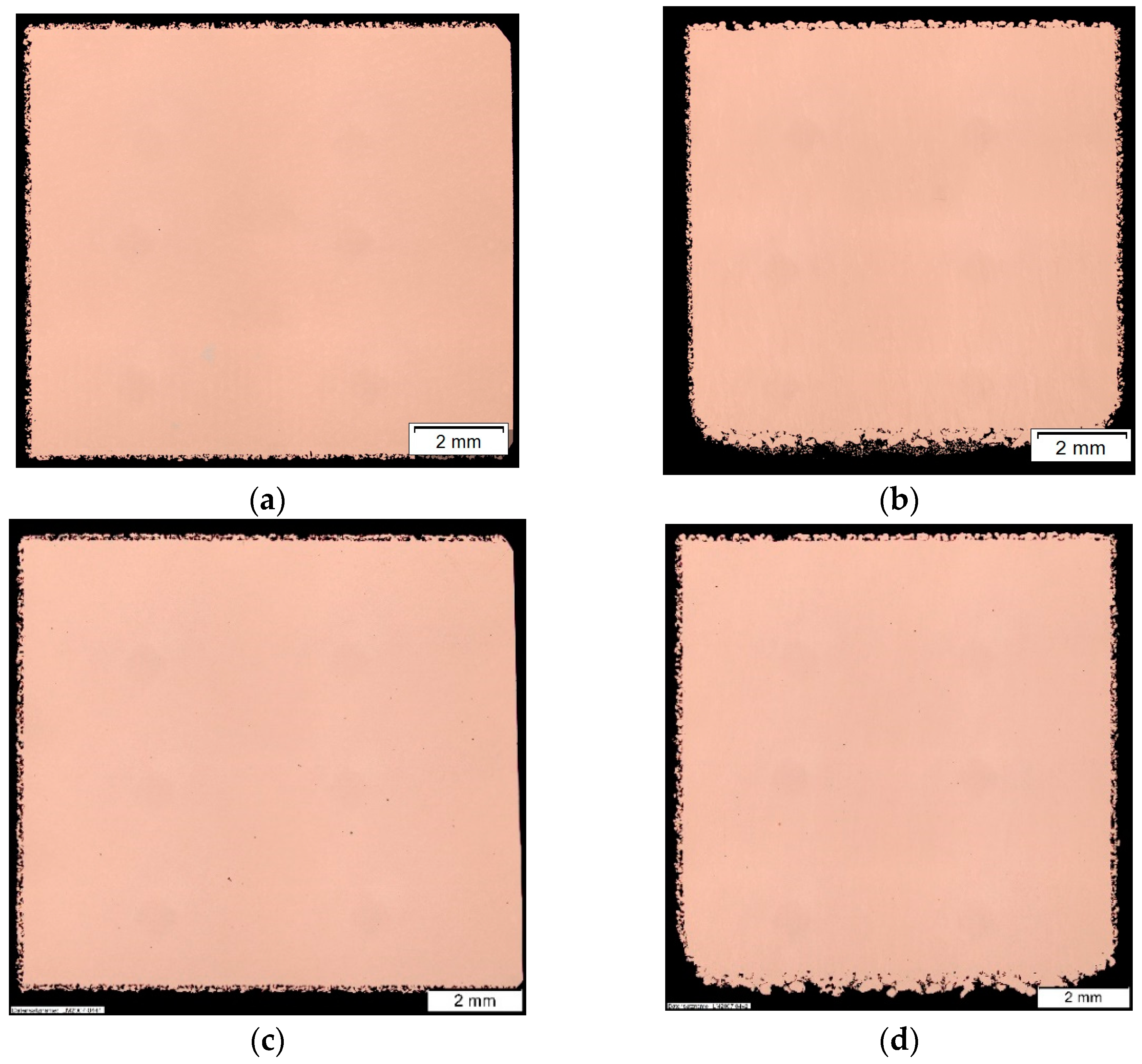
3.2. Porosity
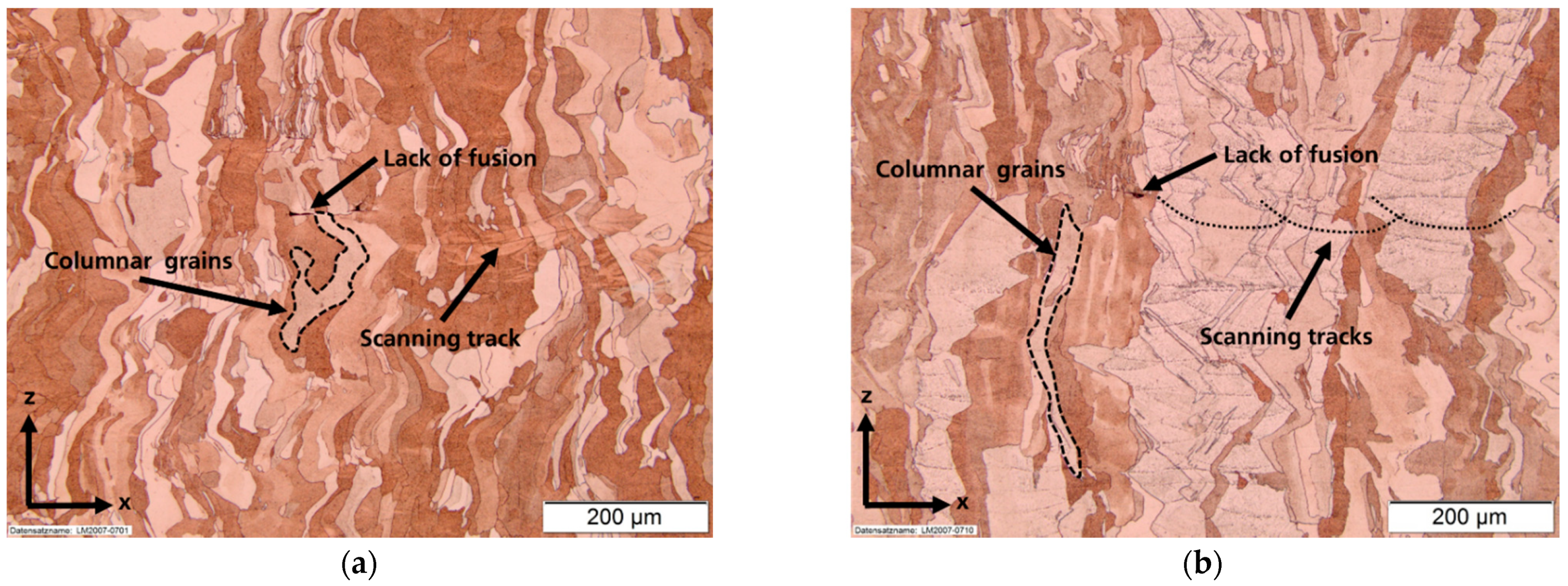
3.3. Microstructure
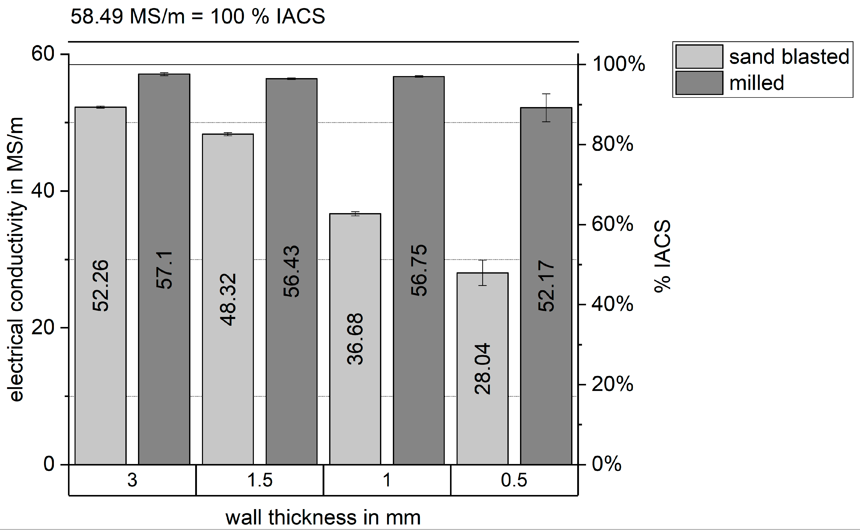
3.4. Electrical Conductivity
3.5. Static Mechanical Properties
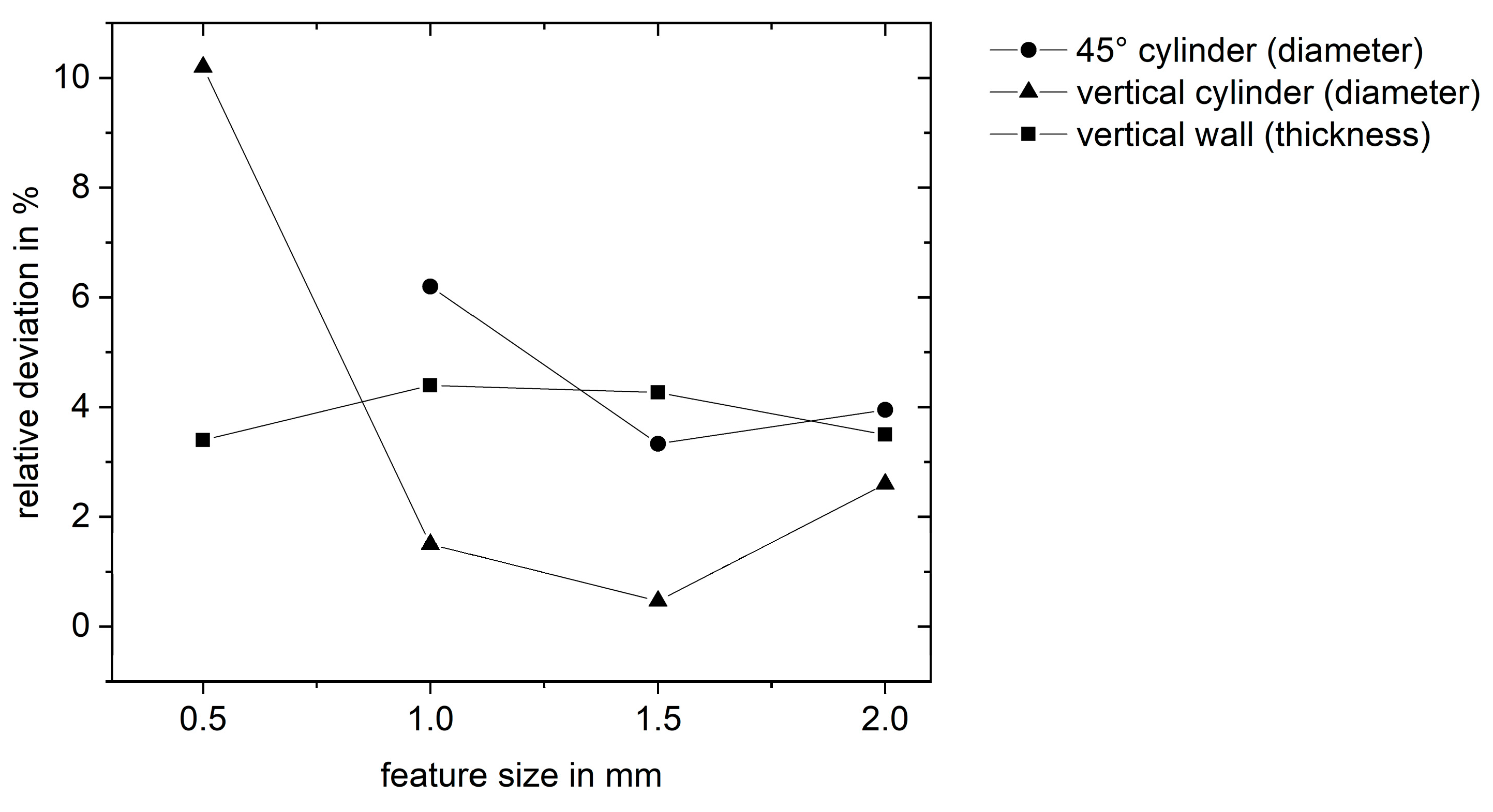
3.6. Geometrical Accuracy
4. Conclusions
- Density above 99.8% and bulk electrical conductivity values of 98.6% IACS and 100% IACS for the two pure copper powders with different particle size distributions were achieved in accordance with [23], proving that the integration of the green laser source into the TruPrint1000 results in a stable process to build high-quality pure copper samples.
- A ground or polished surface with an area of 15 × 15 mm² and a sample thickness of at least 1.5 mm results in a reproducible and correct measurement of the electrical conductivity with the eddy-current method.
- The mechanical properties show anisotropic behavior, which was expected due to the layer-wise build up. The highest strength was found in horizontally build tensile samples.
- Features smaller than 500 µm are difficult to achieve due to the laser focus diameter of 200 µm, the scanning strategy of using contour lines for every feature, and the processing software.
Author Contributions
Funding
Institutional Review Board Statement
Informed Consent Statement
Data Availability Statement
Conflicts of Interest
References
- Lomakin, K.; Guschlbauer, R.; Osmanlic, F.; Fu, Z.; Sippel, M.; Helmreich, K.; Korner, C.; Vossiek, M.; Gold, G. 3D Printed Copper Waveguides by Selective Electron Beam Melting Process for E-Band. In Proceedings of the 49th European Microwave Conference (EuMC), Paris, France, 1–3 October 2019. [Google Scholar]
- Guschlbauer, R.; Burkhardt, A.K.; Fu, Z.; Körner, C. Effect of the oxygen content of pure copper powder on selective electron beam melting. Mater. Sci. Eng. A 2020, 779, 139106. [Google Scholar] [CrossRef]
- Lodes, M.A.; Guschlbauer, R.; Körner, C. Process development for the manufacturing of 99.94% pure copper via selective electron beam melting. Mater. Lett. 2015, 143, 298–301. [Google Scholar] [CrossRef]
- Raab, S.J.; Guschlbauer, R.; Lodes, M.A.; Körner, C. Thermal and Electrical Conductivity of 99.9% Pure Copper Processed via Selective Electron Beam Melting. Adv. Eng. Mater. 2016, 18, 1661–1666. [Google Scholar] [CrossRef]
- Bai, Y.; Williams, C. An exploration of binder jetting of copper. Rapid Prototyp. J. 2015, 21, 177–185. [Google Scholar] [CrossRef] [Green Version]
- Yan, X.; Chang, C.; Dong, D.; Gao, S.; Ma, W.; Liu, M.; Liao, H.; Yin, S. Microstructure and mechanical properties of pure copper manufactured by selective laser melting. Mater. Sci. Eng. A 2020, 789, 139615. [Google Scholar] [CrossRef]
- Silbernagel, C.; Gargalis, L.; Ashcroft, I.; Hague, R.; Galea, M.; Dickens, P. Electrical resistivity of pure copper processed by medium-powered laser powder bed fusion additive manufacturing for use in electromagnetic applications. Addit. Manuf. 2019, 29, 100831. [Google Scholar] [CrossRef]
- Kaden, L.; Matthäus, G.; Ullsperger, T.; Engelhardt, H.; Rettenmayr, M.; Tünnermann, A.; Nolte, S. Selective laser melting of copper using ultrashort laser pulses. Appl. Phys. A 2017, 123, 596. [Google Scholar] [CrossRef]
- Jadhav, S.; Dadbakhsh, S.; Goossens, L.; Kruth, J.-P.; Van Humbeeck, J.; Vanmeensel, K. Influence of selective laser melting process parameters on texture evolution in pure copper. J. Mater. Process. Technol. 2019, 270, 47–58. [Google Scholar] [CrossRef]
- Colopi, M.; Caprio, L.; Demir, A.; Previtali, B. Selective laser melting of pure Cu with a 1 kW single mode fiber laser. Procedia CIRP 2018, 74, 59–63. [Google Scholar] [CrossRef]
- Becker, D. Selektives Laserschmelzen von Kupfer und Kupferlegierungen. Master Dissertation, RWTH Aachen University, Aachen, Germany, 2014. [Google Scholar]
- Colopi, M.; Demir, A.G.; Caprio, L.; Previtali, B. Limits and solutions in processing pure Cu via selective laser melting using a high-power single-mode fiber laser. Int. J. Adv. Manuf. Technol. 2019, 104, 2473–2486. [Google Scholar] [CrossRef]
- Lingqin, X.; Guang, C.; Luyu, Z.; Pan, L. Explore the feasibility of fabricating pure copper parts with low-laser energy by selective laser melting. Mater. Res. Express 2020, 7, 106509. [Google Scholar] [CrossRef]
- Lykov, P.; Safonov, E.; Akhmedianov, A. Selective Laser Melting of Copper. Mater. Sci. Forum 2016, 843, 284–288. [Google Scholar] [CrossRef]
- Zhang, X.; Sun, C.; Pan, T.; Flood, A.; Zhang, Y.; Li, L.; Liou, F. Additive manufacturing of copper–H13 tool steel bi-metallic structures via Ni-based multi-interlayer. Addit. Manuf. 2020, 36, 101474. [Google Scholar] [CrossRef]
- Prasad, H.S.; Brueckner, F.; Volpp, J.; Kaplan, A.F.H. Laser metal deposition of copper on diverse metals using green laser sources. Int. J. Adv. Manuf. Technol. 2020, 107, 1559–1568. [Google Scholar] [CrossRef] [Green Version]
- Asano, K.; Tsukamoto, M.; Sechi, Y.; Sato, Y.; Masuno, S.-I.; Higashino, R.; Hara, T.; Sengoku, M.; Yoshida, M. Laser metal deposition of pure copper on stainless steel with blue and IR diode lasers. Opt. Laser Technol. 2018, 107, 291–296. [Google Scholar] [CrossRef]
- Boley, C.D.; Khairallah, S.A.; Rubenchik, A.M. Calculation of laser absorption by metal powders in additive manufacturing. Appl. Opt. 2015, 54, 2477–2482. [Google Scholar] [CrossRef] [PubMed]
- El-Wardany, T.; She, Y.; Jagdale, V.; Garofano, J.K.; Liou, J.; Schmidt, W. Challenges in 3D Printing of High Conductivity Copper. In Proceedings of the ASME 2017 International Technical Conference and Exhibition on Packaging and Integration of Electronic and Photonic Microsystems, San Franeisco, CA, USA, 29 August–1 September 2017. [Google Scholar]
- Tran, T.Q.; Chinnappan, A.; Lee, J.K.Y.; Loc, N.H.; Tran, L.T.; Wang, G.; Kumar, V.V.; Jayathilaka, W.A.D.M.; Ji, D.; Doddamani, M.; et al. 3D Printing of Highly Pure Copper. Metals 2019, 9, 756. [Google Scholar] [CrossRef] [Green Version]
- Trevisan, F.; Calignano, F.; Lorusso, M.; Lombardi, M.; Manfredi, D.; Fino, P. Selective laser melting of chemical pure copper powders. In Proceedings of the Euro PM2017 Congress & Exhibition, Milan, Italy, 1–5 October 2017. [Google Scholar]
- TIkeshoji, T.-T.; Nakamura, K.; Yonehara, M.; Imai, K.; Kyogoku, H. Selective Laser Melting of Pure Copper. JOM 2018, 70, 396–400. [Google Scholar] [CrossRef]
- Wagenblast, P.; Myrell, A.; Thielmann, M.; Scherbaum, T.; Coupek, D. Additive manufacturing with green disk lasers. In Laser 3D Manufacturing VII, Proceedings of the Society of Photo-Optical Instrumentation Engineers (SPIE) Conference Series, San Francisco, CA, USA, 1–6 February 2020; Gu, B., Chen, H., Helvajian, H., Eds.; SPIE—International Society for Optics and Photonics: Bellingham, WA, USA, 2020; p. 18. [Google Scholar] [CrossRef]
- Lopez, E.; Felgueiras, T.; Grunert, C.; Brückner, F.; Riede, M.; Seidel, A.; Marquardt, A.; Leyens, C.; Beyer, E. Evaluation of 3D-printed parts by means of high-performance computer tomography. J. Laser Appl. 2018, 30, 032307. [Google Scholar] [CrossRef]
- Gruber, S.; Grunert, C.; Riede, M.; López, E.; Marquardt, A.; Brueckner, F.; Leyens, C. Comparison of dimensional accuracy and tolerances of powder bed based and nozzle based additive manufacturing processes. J. Laser Appl. 2020, 32, 032016. [Google Scholar] [CrossRef]
- ASTM E1004-17. Test Method for Determining Electrical Conductivity Using the Electromagnetic (Eddy-Current) Method; ASTM International: West Conshohocken, PA, USA, 2017. [Google Scholar]
- Gu, D.; Yang, Y.; Xi, L.; Yang, J.; Xia, M. Laser absorption behavior of randomly packed powder-bed during selective laser melting of SiC and TiB2 reinforced Al matrix composites. Opt. Laser Technol. 2019, 119, 105600. [Google Scholar] [CrossRef]
- DIN EN 13599:2014-12. Kupfer und Kupferlegierungen-Platten, Bleche und Bänder aus Kupfer für die Anwendung in der Elektrotechnik; Deutsche Fassung EN_13599:2014; VDE Verband der Elektrotechnik Elektronik Informationstechnik e.V.: Frankfurt am Main, Germany, 2014. [Google Scholar]


| Powder | D10 in µm | D50 in µm | D90 in µm | Sphericity |
|---|---|---|---|---|
| Cu-OFHC | 31.6 | 41.5 | 50.1 | 0.919 |
| Cu-ETP | 19.5 | 26.2 | 34.9 | 0.923 |
| Supplier Information | Hot Gas Extraction | Technical Specification DIN CEN/TS 13388 | |||
|---|---|---|---|---|---|
| Cu | H | N | O | O | |
| in wt. % | in ppm | in % | |||
| Cu-OFHC | 99.95 | 10 | 100 | 230 | 1 |
| Cu-ETP | 99.97 | 10 | 30 | 270 | 0.04–0.06 |
| Powder | A at 515 nm | A at 1064 nm |
|---|---|---|
| Cu-OFHC | 72.21% | 27.27% |
| Cu-ETP | 76.93% | 31.99% |
| Powder | Mean Porosity in % | Mean Max. Pore Size in µm | Mean Porous Layer Thickness in µm |
|---|---|---|---|
| Cu-OFHC | 0.017 ± 0.0243 | 410.0 ± 8.50 | 152 ± 17.1 |
| Cu-ETP | 0.013 ± 0.0094 | 52.5 ± 27.59 | 144 ± 35.5 |
| MS/m | % IACS | |
|---|---|---|
| Cu-OFHC | 58.12 ± 0.26 | 100.0 ± 0.44 |
| Cu-ETP | 57.34 ± 0.26 | 98.6 ± 0.44 |
| Condition (Building Direction or Conventional) | Young’s Modulus E in GPa | Yield Strength Rp0.2 in MPa | Ultimate Tensile Strength Rm in MPa | Elongation at Break A in % |
|---|---|---|---|---|
| Vertical | 130.6 ± 27.6 | 135.7 ± 2.3 | 212.3 ± 3.8 | 51.5 ± 8.4 |
| Diagonal | 90.0 ± 9.6 | 127.3 ± 2.1 | 187.7 ± 2.1 | 47.0 ± 3.2 |
| Horizontal | 144.3 ± 15 | 134.8 ± 2.5 | 224.3 ± 2.2 | 47.4 ± 3.5 |
| Soft annealed Cu-OF acc. to [28] | 110 | <100 | 200–250 | 40–60 |
Publisher’s Note: MDPI stays neutral with regard to jurisdictional claims in published maps and institutional affiliations. |
© 2021 by the authors. Licensee MDPI, Basel, Switzerland. This article is an open access article distributed under the terms and conditions of the Creative Commons Attribution (CC BY) license (https://creativecommons.org/licenses/by/4.0/).
Share and Cite
Gruber, S.; Stepien, L.; López, E.; Brueckner, F.; Leyens, C. Physical and Geometrical Properties of Additively Manufactured Pure Copper Samples Using a Green Laser Source. Materials 2021, 14, 3642. https://0-doi-org.brum.beds.ac.uk/10.3390/ma14133642
Gruber S, Stepien L, López E, Brueckner F, Leyens C. Physical and Geometrical Properties of Additively Manufactured Pure Copper Samples Using a Green Laser Source. Materials. 2021; 14(13):3642. https://0-doi-org.brum.beds.ac.uk/10.3390/ma14133642
Chicago/Turabian StyleGruber, Samira, Lukas Stepien, Elena López, Frank Brueckner, and Christoph Leyens. 2021. "Physical and Geometrical Properties of Additively Manufactured Pure Copper Samples Using a Green Laser Source" Materials 14, no. 13: 3642. https://0-doi-org.brum.beds.ac.uk/10.3390/ma14133642