Article

A Comparative Study on p- and n-Type Silicon Heterojunction Solar Cells by AFORS-HET

by
Wabel Mohammed Alkharasani
1,
Nowshad Amin
1,*,
Seyed Ahmad Shahahmadi
2,*,
Ammar Ahmed Alkahtani
1,
Ili Salwani Mohamad
1,
Puvaneswaran Chelvanathan
3 and
Tiong Sieh Kiong
1
1
Institute of Sustainable Energy (ISE), Universiti Tenaga Nasional, Jalan IKRAM-UNITEN, Kajang 43000, Malaysia
2
Engineered Nanosystems Group, School of Science, Aalto University, 00076 Aalto, Finland
3
Solar Energy Research Institute (SERI), Universiti Kebangsaan Malaysia (UKM), Bangi 43600, Malaysia
*
Authors to whom correspondence should be addressed.
Submission received: 11 February 2022 / Revised: 6 March 2022 / Accepted: 8 March 2022 / Published: 13 May 2022
(This article belongs to the Topic Nanomaterials for Sustainable Energy Applications)

Abstract

:
Despite the increasing trend of n-type silicon wafer utilization in the manufacturing of high-efficiency heterojunction solar cells due to the superior advantages over p-type counterparts, its high manufacturing cost remains to be one of the most crucial factors, which impedes its market share growth with state-of-the-art silicon heterojunction (SHJ) solar cells demonstrating high conversion efficiencies from various configurations, the prospect of using an n-type wafer is debatable from a cost-efficiency point of view. Hence, a systematic comparison between p- and n-type SHJ solar cells was executed in this work using AFORS-HET numerical software. Front and rear-emitter architectures were selected for each type of wafer with ideal (without defects) and non-ideal (with defects) conditions. For ideal conditions, solar cells with p-type wafers and a front-emitter structure resulted in a maximum conversion efficiency of 28%, while n-type wafers demonstrated a maximum efficiency of 26% from the rear-emitter structure. These high-performance devices were possible due to the optimization of the bandgap and electron-affinity for all passivating and doping layers with values ranging from 1.3 to 1.7 eV and 3.9 to 4 eV, respectively. The correlation between the device structure and the type of wafers as demonstrated here will be helpful for the development of both types of solar cells with comparable performance.

1. Introduction

The idea of heterojunction silicon solar cells in both amorphous and crystalline configurations was introduced first by Fuhs et al. in 1974 [1], and it later came into reality in 1983 when Hamakawa et al. reported a successful amorphous device with more than 9% power conversion efficiency (PCE) [2]. A decade after, Sanyo Ltd. reported the first heterojunction with an intrinsic thin layer (HIT) using silicon wafers in 1991 reaching an efficiency of 18.1% [3].
Since then, several laboratories have actively adopted and explored HIT configurations for further improvement. The primary motivation for this technology comes from the ability to achieve highly efficient cells with low-processing temperature, comparatively low fabrication costs, and optimum surface passivation [4]. Historically, n-type wafers dominated the HIT research and industrial arena [5]. The highest PCE obtained in HIT solar cells used n-type crystalline silicon (c-Si) wafer, whose effectiveness was higher than a p-type wafer [6].
This is associated with higher carrier lifetimes, a reduction in light-induced degradation (LID) caused by the formation of boron-oxygen or iron-boron complexes, and not solely relying on the process to enhance the bulk lifetime [7,8,9]. However, recent studies linked with annealing effects in high temperatures within the p-type process, which are capable of reducing LID, and they proved to have successful implementations [9,10,11,12]. Basic problems within the band structure, such as asymmetry offset among the conduction and the valence band (Ec and EV), cause the p-type to be less efficient than the n-type as A. Descoeudres reported this in a paper published in 2013 [13].
This asymmetry in the band offset triggers a unique recombination reaction in p-type and n-type cells. Large EV offset (∆EV) is preferred in n-type wafers, as it minimizes the minority carriers (holes) interfacial recombination probabilities. On the contrary, a small EC offset (∆EC) in p-type increases the minority carriers (electrons) interface recombination possibility to occur. Typical n-type wafers are well known to have a better lifetime when compared with p-type wafers. This advantage is recognized from lower defect density and impurities, which enables unwanted recombination. Additionally, n-type Si-doped purely with phosphorus is more resistant to degradation compared to boron-oxygen (B-O) complexes in p-type.
However, recent investigations indicated that these degradation dynamics could also be found in low-cost n-type wafers as well [14,15]. Currently, p-type wafers are frequently utilized in homojunction cells whether in passivated emitter and rear cell (PERC) design or aluminum back surface field (Al-BSF) solar cells due to the low cost and process simplicity. The cost to produce n-type ingots is considerably higher than for p-type. According to Wang in 2018, it costs 8% more to manufacture n-type wafers [16,17,18]. For now, n-type wafer-based silicon solar cells are less likely to be found in the market compared to p-type. It is still expected for n-type based silicon cells to gain greater market share within the next ten years [19].
It is of great practical importance in manufacturing high-efficiency HIT cells from p-type wafers. Several cells of this form have already shown the possibilities to be made with substantially less PCE than those obtained from wafers of n-type [5,20,21,22,23,24,25]. A variety of studies have already been carried out as mentioned above, which address p- and n-type wafer-based cells, and some are worthy to be mentioned, such as the review De Wolf et al. [6] presented in 2012. They highlighted the fabrication process and its challenges as well as a comparison of different types of structures with results from different groups.
Another excellent study from Descoeudres et al. [13] was published in 2013. They fabricated two types of cells based on p- and n-type Si wafers. The PCEs of 21.38% for p-type and 22.14% for n-type cells were reported or the recent article in 2019, where 23.76% and 24.21% cells were fabricated, respectively [16]. The current highest HIT solar cell is based on the n-type c-Si wafer with 25.1% by Daisuke et al. in 2015 and Xiaoning et al. in 2020 with some structural optimizations [26,27]. Although silicon solar cells yet dominate the market [19], many studies are shifting towards a variety of thin-film solar cells, including CdTe, CIGS, perovskites, and various polymers.
Bhattacharya and John [28] presented a new promising methodology that would result in a flexible, high-efficiency thin-film solar cell. However, the presented process is still considered to be complex, and it would cause the fabrication process to be costly. Other groups have focused on the new novel field of perovskites [29,30]. Perovskites proved to have the potential to be the leading technology in the future. However, they are still facing some stability issues [31].
Thus, this study focuses on the HIT considering the market acceptances, device stability, production simplicity, and cost-effective procedures with high-efficiency devices [16]. For further improvement of the HIT’s PCE, some factors should be considered and understood carefully before any optimization. The kind of parameters that affect HIT solar cells, such as the structure, thickness, doping concentration, minority carrier lifetime, resistivity, recombination losses, parasitic absorption loss, and defects, usually have a significant effect on the solar cell operation outcome [32,33,34,35,36].
Silicon heterojunction studies are usually focused on different aspects of parameter optimization of a-Si as the thin layer for passivation as well as buffer layers or introducing buffer layers [37,38,39,40,41]. In this work, we address the possible effects in PCE or potential limitations in four different HIT structures with defects in three different locations across the bandgap (Eg) of each layer in a systematic comparison of p- and n-type wafers to understand the effects of defects in various HIT structures using AFORS-HET software [42].

2. Methodology

AFORS-HET is considered an essential simulation tool when it comes to heterojunction modeling, especially for silicon solar cells. It utilizes one-dimensional semiconductor equations that are associated with Shockley–Read–Hall statistics, and solves them numerically. As shown in Figure 1, four established HIT silicon solar cells are considered from the literature [13,16]. They are designed based on the two types of wafers, which are n and p-type, the emitter location differs as well, and thus it will be either at the front side (front-emitter cell) or the backside (rear-emitter cell).
Hence, the potential difference in charge carrier transport across the entire proposed structures can be discussed. As shown, the structures simply contain a c-Si wafer sandwiched between passivating and doped layers. We assumed that the passivating and doping layers have various band gaps and electron affinities. The Eg is varied between 1.1 to 2.2 eV, while the electron affinity (χ) is chosen from 3.8 to 4.2 eV. Varying the Eg and electron affinity provides a better understanding of the effect of the hydrogen content during fabrication on the cell’s performance. From the experimental point of view, HIT cells are now the best in utilizing passivation contact structures.
The intrinsic hydrogenated amorphous silicon (a-Si:H) layer is the key component behind the superiority of this structure as it provides outstanding chemical passivation for the absorber. It also can be doped to be p or n-type [43] which could influence an adequately large c-Si surface potential to attain carrier selectivity (electron collection for n-a-Si:H overlayers and hole collection for p-a-Si:H overlayers). The a-Si:H is a direct Eg material that depends on the degree of hydrogen incorporation during deposition and could result in Eg ranging from 1.5 to 2.0 eV [44,45,46]. As a result, a-Si:H is an excellent material in creating carrier selective contact passivation that works effectively. Furthermore, in a completely formed silicon heterojunction solar cell, there is a remarkable inversion charge at the a-Si:H/c-Si interface, which assists in c-Si surface field-effect passivation.
Such intrinsic properties could face some offsets due to the extremely high parasitic optical absorption and the difficulty in managing the barrier heterojunction between the a-Si:H/c-Si interface, motivating a continuous search for novel passivation materials. That is another core objective of this study, which is to evaluate the possibility of finding any promising materials in the range of our variation, which are capable of replacing the a-Si:H and provide competitive performance. This variation would likely expound any effect that might occur due to different band offset in absorber or buffer regions on the overall cell performance.
There are a few noticeable differences in the structural parameters, which can be seen in Table 1 that represent the material properties used in the software for each layer. For instance, oxygen defects in p-type c-Si substrate have a density of 1 × 1010 cm−3 eV−1 and are located at 0.55 eV above EV to represent the carrier lifetime of 1 ms. Typically, carrier recombination through defects is presumed to occur by a Shockley–Read–Hall two charge state level. Yet, the silicon dangling bond appears to be the source of interface recombination. At equilibrium, depending on the location of the Fermi level, these defects might be in a neutral, positively charged, or negatively charged state.
Increased doping level could also result in higher defect density, pinning the Fermi level [6]. In the present simulation, three different locations of defects are chosen and set within the Eg where their distributions are depicted in Figure 2. The defects are Gaussian type and acceptor or donor charges with trap density of 1.99 × 1020 cm−3 eV−1 and 0.02 eV energy of distribution. The first location is 0.2 eV above the EV, while the second location is exactly at the middle of Eg and the final location at 0.2 eV below the EC. The ideal device with no defects was assumed to determine the best region from the Eg and the χ. Later, the full potential of each structure is investigated.

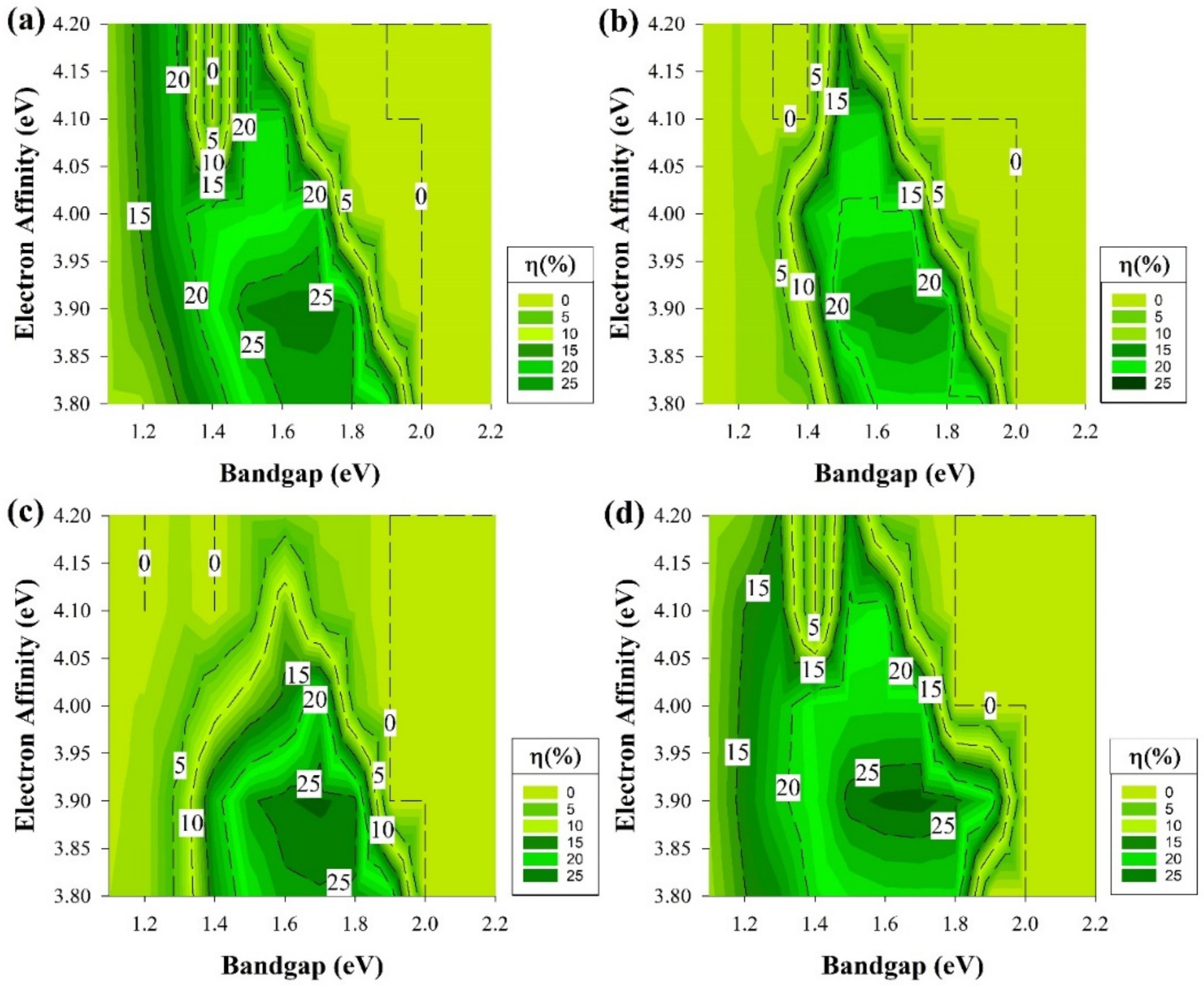
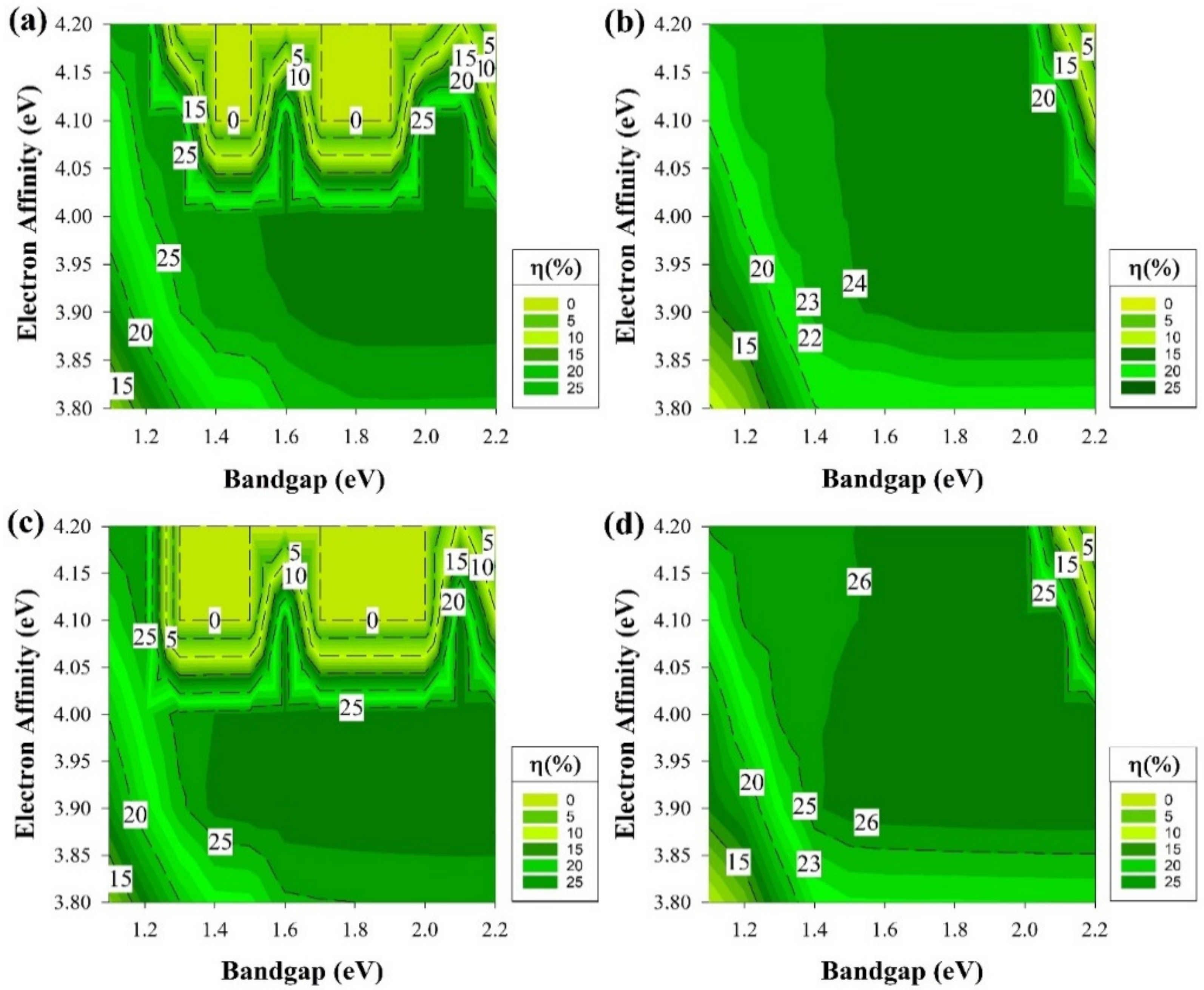
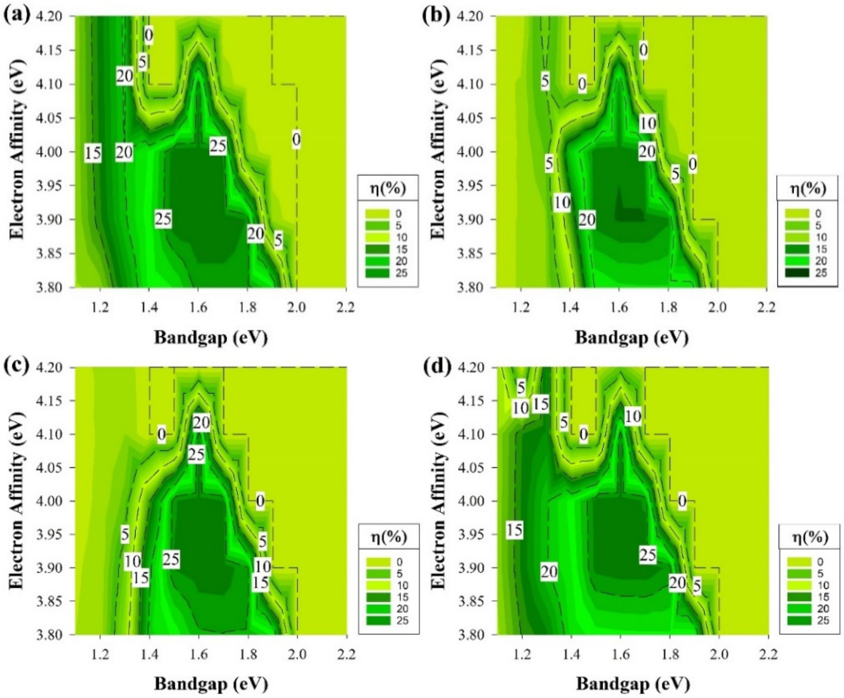
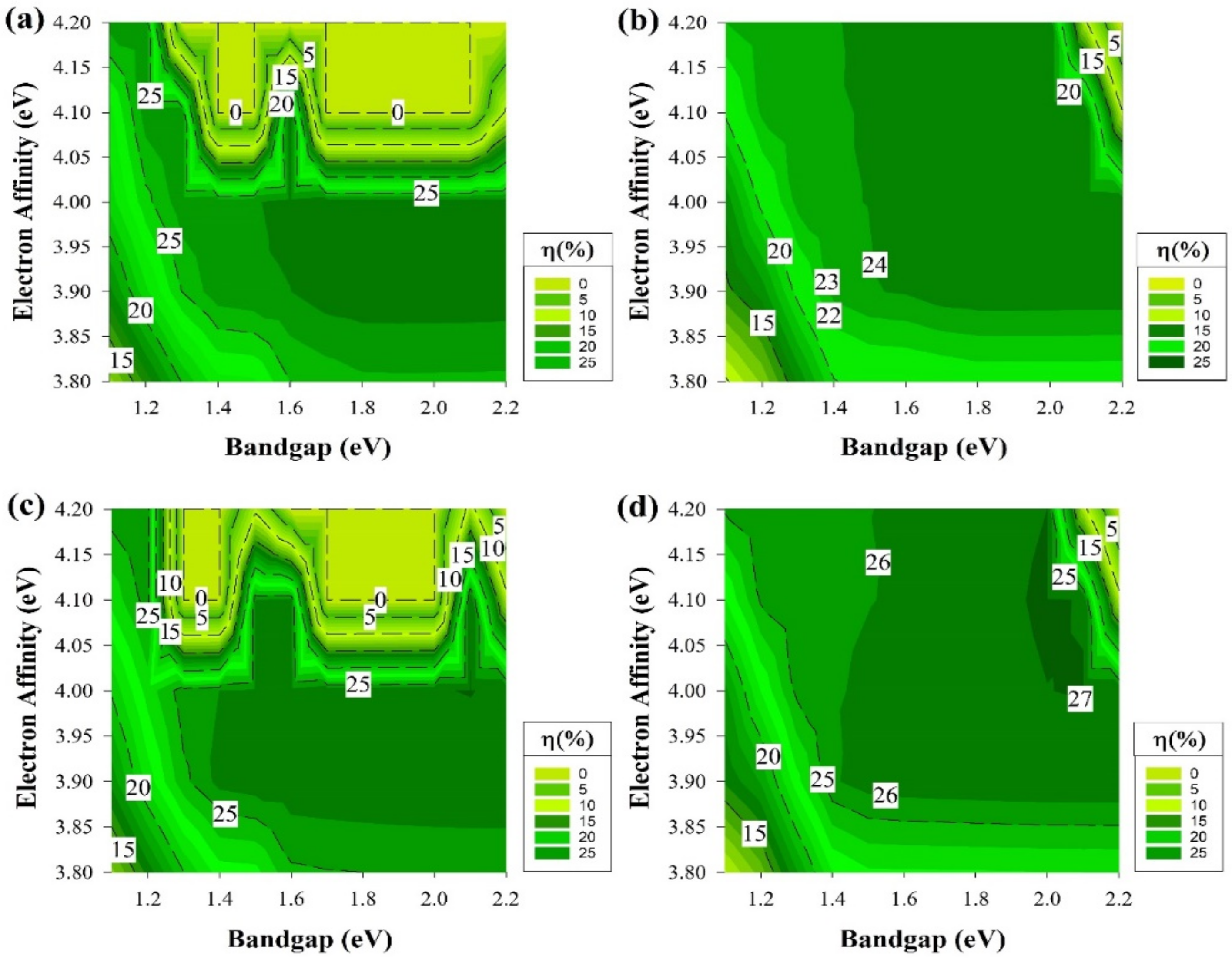
3. Results and Discussion

The highest reported PCE among HIT cells is considered as the benchmark for this study. The obtained electrical results are similar to what has been reported in other works of literature [26,27,47]. The results are divided into separate sections that follow the conditions of the simulation. The first part represents the results of varying the Eg and χ of the emitter, BSF, and buffer layers without any defects.

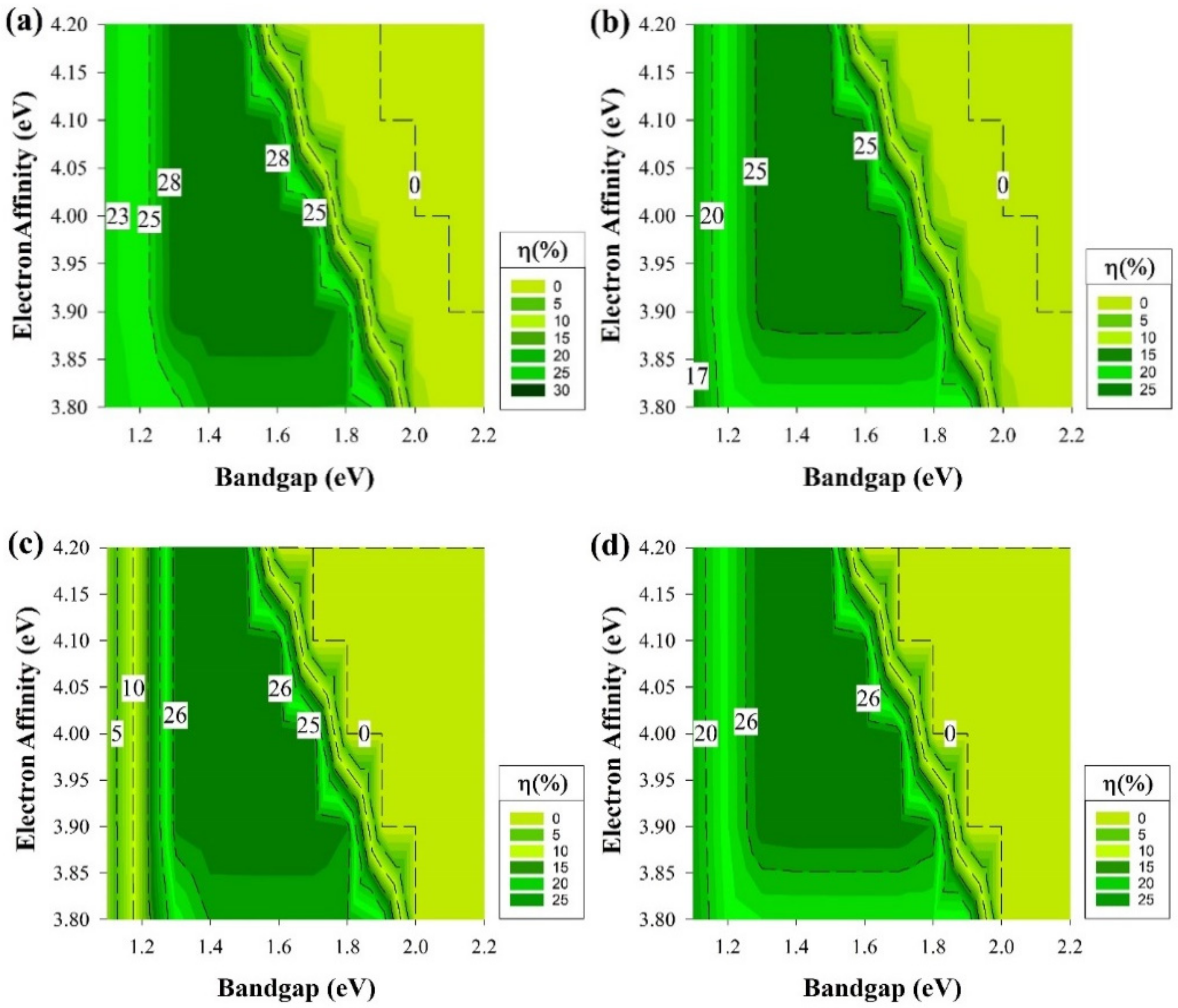
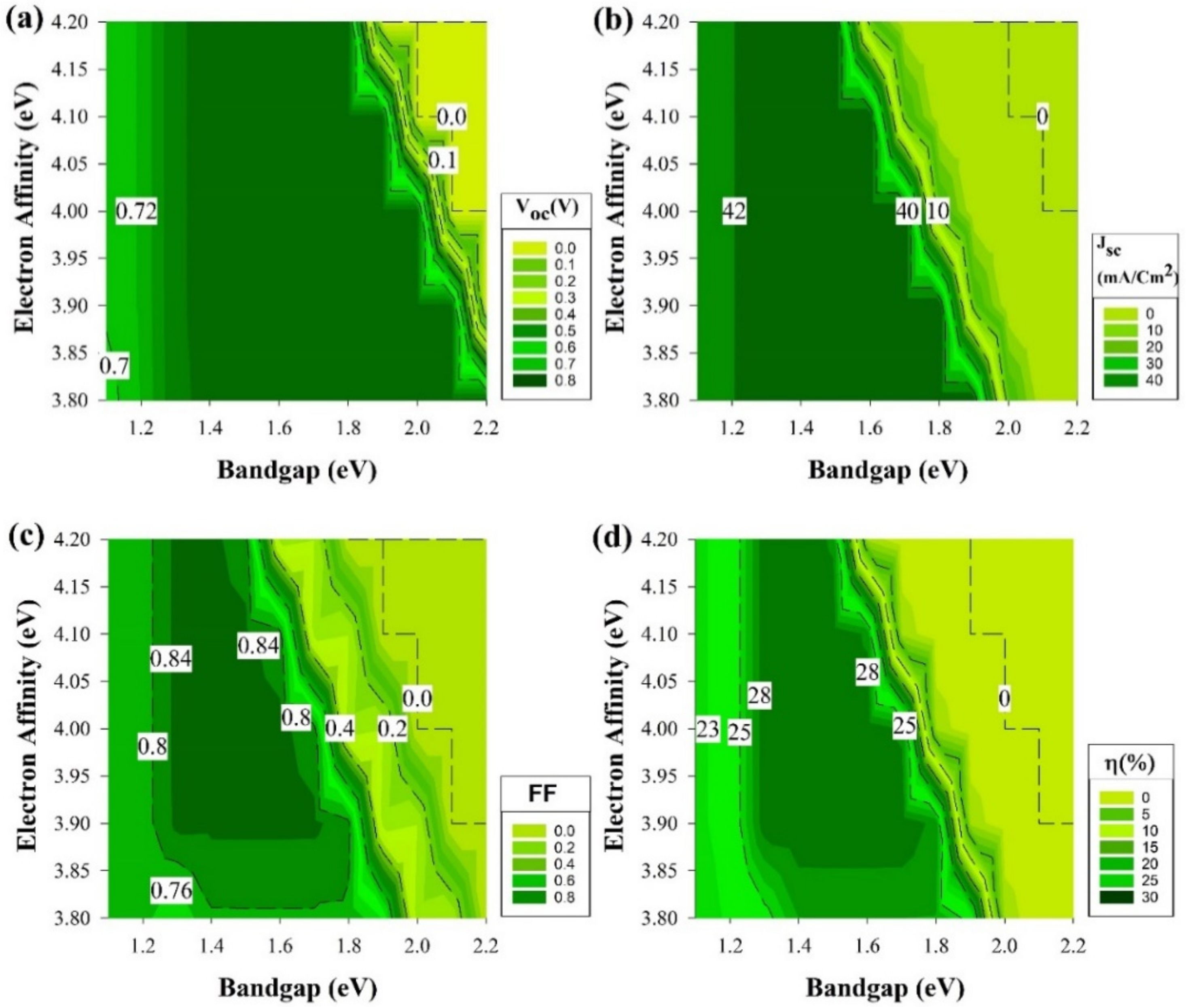
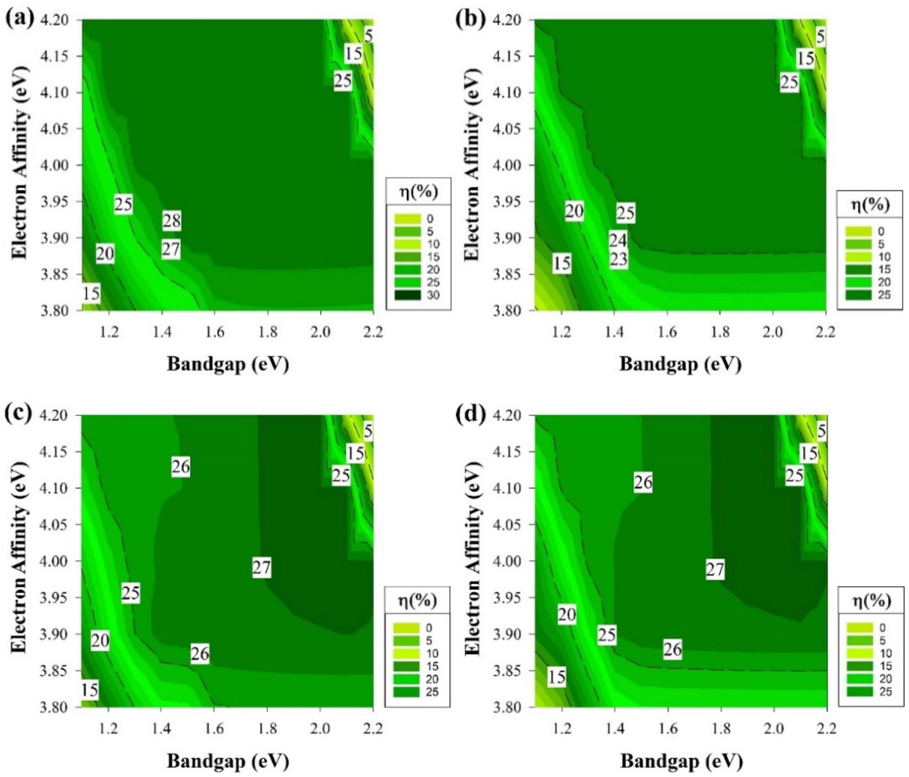
3.1. Ideal Case without Defects

Figure 3 depicts the cell efficiency performances of the four structures that are shown in Figure 1. The top left (Figure 3a) represents the performance of the structure in Figure 1a. In this figure, the maximum PCE reached 28% in the Eg region from 1.3 to 1.7 eV all over χ axis except when the χ is lesser than 3.85 eV or more than 4.1 eV as the PCE dropped to be lesser than 25% for the first with a dramatic drop for the second with Eg more than 1.5 eV. The region below 1.3 eV of the Eg is still an active region but with a lower performance with an average of 23%.
The dead zone is always after 2 eV in the Eg or at higher χ (≥4.1) when Eg = 1.7 eV. Figure 3b,d are almost identical but with an extra 1% in the highest PCE achieved for Figure 3d. Both of the figures still follow the same trend of Figure 3a where the highest performance is still in the region from Eg = 1.3 eV to 1.7 eV. The dead zone is still in the zone after 2 eV in the Eg or at higher χ (≥4.1) when Eg = 1.7 eV as well. While the region below 1.3 eV of the Eg is also performing in a lesser amount in terms of PCE but still higher than 15%.
However, Figure 3c still follows the same trend as the rest of the graphs where the highest area in the range from Eg = 1.3 eV to 1.7 eV, on the other hand, when χ is lesser than 3.85 eV or more than 4.1 eV, the PCE drops. As well as for the dead zone to be after 2 eV for the Eg or at higher χ (≥4.1 eV) when Eg= 1.7 eV. The only difference experienced is at the range below 1.3 eV from the Eg as the PCE reach as low as 2%, the reason behind this observation will be discussed later on. The trend shown in Figure 3 indicates that some conditions would provide a better cell performance rather than others and demonstrates the potential for new materials with the same properties to be used as a buffer layer, such as i-μc-Si:H [48].
To obtain a better understanding of the results in Figure 3, a deeper analysis of the solar cell performance is required. Therefore, the rest of the cell electrical parameters have been shown in Figure 4 from the structure, which delivers the highest performance that belongs to the structure of Figure 1a. Though there are four different structures, the exact trend from Figure 3 is still the same and applicable for the rest of cell’s performance parameters, and these results are shown in Figure 4 mainly because, on both wafer types, the short-circuit current (Jsc) measurements are almost identical and reach as high as 43 mA/cm2 since the cells’ absorptions of light are similar.
The ITO and wafer and thicknesses are the same, while p/n-doped a-Si:H layers have identical optical absorption properties [49] and thicknesses. Thus, the outcomes of analyzing one structure would apply to the rest of the structures as they follow the same trend in every aspect of the results obtained.
Figure 4 shows four common performance parameters of a solar cell, open-circuit voltage (Voc) in Figure 4a, the Jsc in Figure 4b, fill factor (FF) in Figure 4c, and solar cell PCE or η in Figure 4d. In Figure 4a, the Voc has its maximum value of 785 mV at the Eg from 1.3 to 2.1 eV, while the χ is less than 3.9 eV. The area below 1.3 eV Eg results in Voc around 720 mV irrespective of the χ. The inactive areas are at χ of 3.9 to 4.2 eV and a high value of Eg in the vicinity of 2 eV.
The first look at Figure 4b would remind us of the trend in Figure 3 since the active part is until 1.8 eV in the Eg axis but this graph represents the Jsc where most of the active part has a value of 43 mA/cm2 except when Eg is less than 1.2 eV as the value would be in the average of 41 mA/cm2. As for the dead zone where the values are almost zero or equal to zero, Eg (≥2) has mostly been the region in this section of the study. In Figure 4c, the maximum FF (80%) was calculated in the range of Eg =1.3 to 1.6 eV with χ = 3.9 eV onwards and at χ of ≥4.15 eV, the Eg region reduces from 1.3 to 1.5 eV. Finally, Figure 4d is as same as Figure 3a detailed above.
It is known that a higher Eg value will cause Jsc to decrease. However, the higher the Eg, the higher the Voc, based on the equation below.
V oc = E g q kT q ln J sc J 00
where J00, K, T, and q are the saturation current, Boltzmann constant, temperature, and electron charge, respectively [50]. A minority carrier current (Jn) is a crucial element, which affects the solar cells’ performance. While having a bias voltage Vb, the electron minority carrier current is represented by
J n = J n 0 1 + v × e qV b kT
where
J n 0 = KT μ n 1 L n 1 n 1
where Ln, µn, and n1 are the diffusion length, minority-carrier mobility, and concentration, correspondingly. The subscript 1 denotes the depletion region extended in p-type material (Si in our case). The factor ‘ v ’ shown in Equation (2) states the impact of the ∆EC on the minority carrier electron current and is presented by
v = 1 L n 1 x 1 x 2 μ n 1 N c 1 μ n N c e E c 1 E c + q Ψ kT   dx
where x1 < 0 to x2 > 0 is the depletion region extended from c-Si to a-Si, and Ψ(x) is the potential function. The subscripts 1 and 2 are c-Si and a-Si material, respectively. The abrupt pn heterojunction with applied bias near-zero, solving Equation (4) would be as below.
v = I v 1 L n 1 + 1 L n 1 μ n 1 N c 1 μ n N c I v 2 × e E c 1 E c 2 kT
where       I v 1 = x 1 0 e q Ψ x kT   dx
and       I v 2 = 0 x 2 e q Ψ x kT   dx
The potential function could be assumed to be decoupled by the carrier transport equations and it follows Poisson’s equation as:
d 2 Ψ dx 2 = ρ Ψ ϵ
where ρ is charge distribution and ϵ is the permittivity of the medium. The electrostatic potential Ψ(x) obtained from Equation (8) is used in solving Equations (2)–(7) for a wide Eg layer on a narrow Eg layer to have [51].
J n = kT μ n 1 N c 2 n i 1 2 I v 2 N c 1 N A e Δ E c kT e qV kT 1
This confirms that the Jn decreases significantly for a wide Eg layer on a narrow Eg layer (a-Si/ c-Si interface) owing to the ∆EC increase [52]. Table 2 shows the results of the ∆Ev and the ∆ EC at i-a-Si/c-Si interface. As shown in equation 9, the Jn is a function of ∆EC, which can result in a lower value at high ∆EC. The Jn is directly proportional to the Jsc where it decreases and decreases at lower and higher Jsc, respectively. Using equation 1 would explain why the Voc could cover more area in Figure 4a as the Voc increases at higher Eg.
The results of Figure 4b line up after comparing the relationship of Eg and Voc in equation 1 with ∆EC and Jsc in equation 9. As a wide Eg will cause higher Voc but lesser Jn affecting Jsc to be lower as well, ideally, the FF is only a function of Voc [53]. However, the FF might not hinge on the Voc only, the depletion region recombination could play a role as well series resistance losses where those effects are noticeable in Figure 3c as it does not follow the trend of Voc figure. Finally, the PCE = Voc × Jsc × FF equation implies that the PCE is a merge of the three output values mentioned previously and established on the importance of Voc, Jsc, and FF variation in this work.
The effect of ΔEC and ΔEV between the silicon wafer and the intrinsic buffer layer is the main variable that significantly affects the results of Figure 3 specifically the region after Eg (≥2 eV) as the PCE drops to zero. Furthermore, corresponding to the type of doping, an increase in Eg could be found as upshifting of Ec and/or downshifting of Ev and proper shifting of Ef. Variation in the χ moves the entire band structure upward or downward and caused changes in ∆EC. For instance, χ of 4.0 eV with Eg = 1.5 eV has ΔEc and ΔEv of −0.05 eV and 0.33 eV, respectively, as it is shown in Table 2.
Band offsets comprehensive analysis of the a-Si:H/c-Si interface done using photoelectron spectroscopy and surface photovoltage measurements, which been published showed that ΔEC and ΔEV do not depend on substrate and film doping, in all cases being approximately equivalent to 0.15 and 0.45 eV, respectively, while fabricating a cell [54,55]. While other data also showed that ΔEV would increase more if the hydrogen content in a-Si:H is being increased, while ΔEC stays constant [56]. These ΔEC offers a mirroring effect for minority carriers, while the ΔEV creates barriers that cause tunneling of the majority carriers.
The greater ΔEC would cause a potential wall where the minority carrier electrons could be trapped, thus, stopping the process of carrier transport [57]. Overall, at the high values of χ (≥4.1 eV) and Eg (≥1.8 eV), results in Table 2 are positive, which suggests a limitation in electron flow from the lower energy EC of the intrinsic layer to the higher energy EC of c-Si. In contrast, lower χ results in negative ΔEc, which indicates a natural electron flow from the higher energy EC of the intrinsic layer to the lower energy EC of c-Si. This also influences the cell performance at low Eg values, as electron flow might cause a charge carrier recombination [58].
As mentioned above, Figure 3c does not follow the same trend as the rest of graphs in Figure 3 at the region below 1.3 eV in Eg. Thus, Figure 5a depicts the band diagram of this solar cell. A lower ΔEC barrier is observed, and this would cause the electrons (minority carriers) to recombine easily at the interface in the p-type case. There are noticeable losses in FF for this structure, while the emitter is located at the back of the device. The FF ranking of various cells is not affected by series resistance losses only but somehow by something intrinsically connected with the device structure. Voc values are somewhat decreased also, but to a lesser extent. The drop in the device PCE could be caused by the illumination reduction on the emitter side of this rear-emitter cell.
The results from Figure 3 represent the best region of Eg and χ to be used as a buffer layer and the fact that a high-quality fabricated i-a-Si:H buffer layer in HIT will work as an excellent passivation interface layer. This resulted in shaping the foundation of the other part of this study. The section results can be seen in Figure 6 where we assume that we have an ideal i-a-Si:H layer (Eg = 1.7 eV and χ = 3.9 eV) with no defects, which will act as a buffer and passivation layer while keeping the same variation conditions as the previous section regarding the Eg and χ variation at the emitter and BSF.
Therefore, we have the opportunity to study the effects of an ordinary passivation layer on the cell performance while changing Eg and χ in the rest of the layers. The four graphs of Figure 6 follow the same trend as the cell performance starts from lower PCE then become stable values and start to decrease again after Eg is more than 2.1 eV and χ is higher than 4 eV.
The results of Figure 6 indicate a huge improvement in the overall performance across different bandgaps and affinities. This is mostly due to the improvement in the interface layer after fixing the buffer layer of i-a-Si:H to be of Eg of 1.7 eV and χ = 3.9 eV. The band diagram of the system is represented in Figure 5b where ΔEC and ΔEV in these conditions are the same as the fabrication point of view. Using i-a-Si seems to cause a higher built-in voltage at the crystalline absorber while suppressing the interface recombination in the a-Si(emitter)/c-Si heterointerface. As the maximum Voc remains the same in all cells, the JSC increases, with an increase in the overall PCE in structure Figure 1c,d, adding 0.2% more to reach 27.1%.
The band diagram of Figure 5b indicates that the i-a-Si:H layer would hinder the photon carrier recombination from the n-a-Si:H emitter layer to the p-c-Si base layer, which would enhance Jsc and would reflect on the PCE results of the 4 cells. Higher Eg and χ would cause a higher value for ΔEC. This will suppress the movement of electrons causing the cell performance to decay explaining why the performance dropped again when Eg ≥ 2.1 eV and χ ≥ 4 eV. It is clear that the cells still have a trend similar to the previous section, and this indicates that the four structures are useable if they were fabricated specifically.

3.2. Non-Ideal State including Defects for All Passivating and Doped Layers

The results of the second case are shown in Figure 7 and Figure 8. In this part of the study, a defect density of 10−19 cm−3 is introduced to the layers. In the first case, which is represented in Figure 7, all the layers except the Si wafer have a shallow type of defects at 0.2 eV from the EV while keeping the previous conditions of the earlier sections. It is noticeable from Figure 7 that the defects introduced have affected the overall cell performance and reduced the active area in structure n-i-p for p-type Si and p-i-n with n-type Si as illustrated in Figure 7b,c, respectively.
Figure 7b,c are shown a similar trend as they both have an active area in the region from 1.4 to 1.9 eV in the Eg across the different values of χ. While the highest PCE results are when Eg: 1.5–1.8 eV and 3.9 ≤ χ ≤ 4.1. In these two graphs, the PCE is always below 10% and reaches zero when Eg ≤ 1.3 eV for all the χ or when Eg ≥ 2 eV. As for the second region, it is expected to remain as a dead zone since it has been a dead zone when the cell is defect free.
In addition, the region below 1.3 eV has been a low-performance zone in Figure 3c, and the introduction of defects clearly would cause a further reduction in the cell at the same region for Figure 7c results making almost a dead zone for all χ. On the other hand, the graphs of Figure 7a,d are the second patch of trend as the dead zone remains after Eg is higher than 2 eV, but a performance decay is observed when Eg is below 1.5 eV. The highest PCE region is as same as the other two graph locations mentioned above.
Overall, as the defect density was introduced, the PCE was decreased quite dramatically. This was expected because defect states act as detrimental recombination centers for photo-generated charge carriers [59]. Recombination is lowered in the case where the interface recombining carrier’s concentration is kept low. A large band offset in the minority carrier band grants this condition.
It is noticeable from Figure 7 that the shallow defects that we introduced had the most impact on the Eg values below 1.5 eV through the different structures; however, the unique remark is that the cells with rear emitter endure a severe effect at the same region. This could be a result due to a greater loss in the FF for this type of structure [13]. FF has always been related to series resistance losses; however, the rear emitter structure showed a greater loss, which indicates that this type of structure could experience higher series resistance losses or might be due to the structure layers themselves.
Similar to the earlier section, the second part will address the results while having the ideal passivation layer of i-a-Si, assuming that this layer is perfectly deposited without any defects while adding the shallow defect of the same density stated above to the remaining layers and keeping the Eg and χ as variables. All the cell performance simulation results of this segment are depicted in Figure 8. At the first glance at Figure 8, it is clear that it is almost the same as Figure 6 but with some PCE drop within the middle area of Figure 8a and b, which is higher than 1.5 eV of Eg but lower than 2.1 eV at χ higher than 4 eV.
The other two graphs only undergone a decrement of the highest PCE to go from the area started at 1.8 eV to nearly 2.2 eV whilst the χ is lower than 4 eV as it is demonstrated in Figure 6c,d, to shrink and have a small portion located between Eg 2–2.1 eV with χ ≥ 4 eV. By comparing Figure 6 and Figure 8, the advantages of using an intrinsic a-Si layer in a heterojunction structure are spotted. The PCE degradation is expected to occur since defects have been added. This layer suppresses the effect of shallow defects near the EV and allows the cell to provide comparable performance as if there were no defects of this type in the Eg.

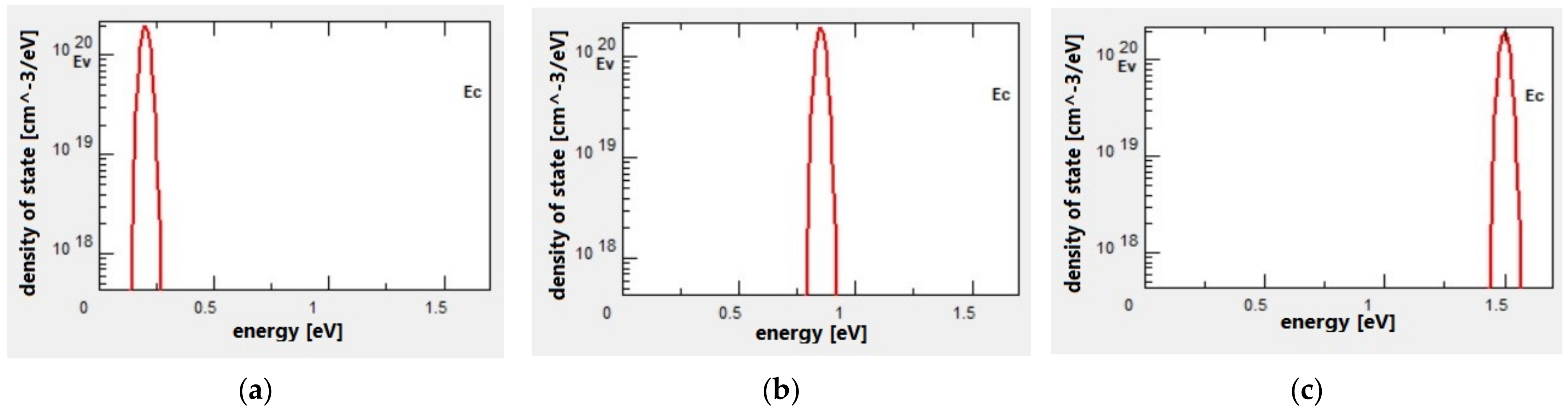
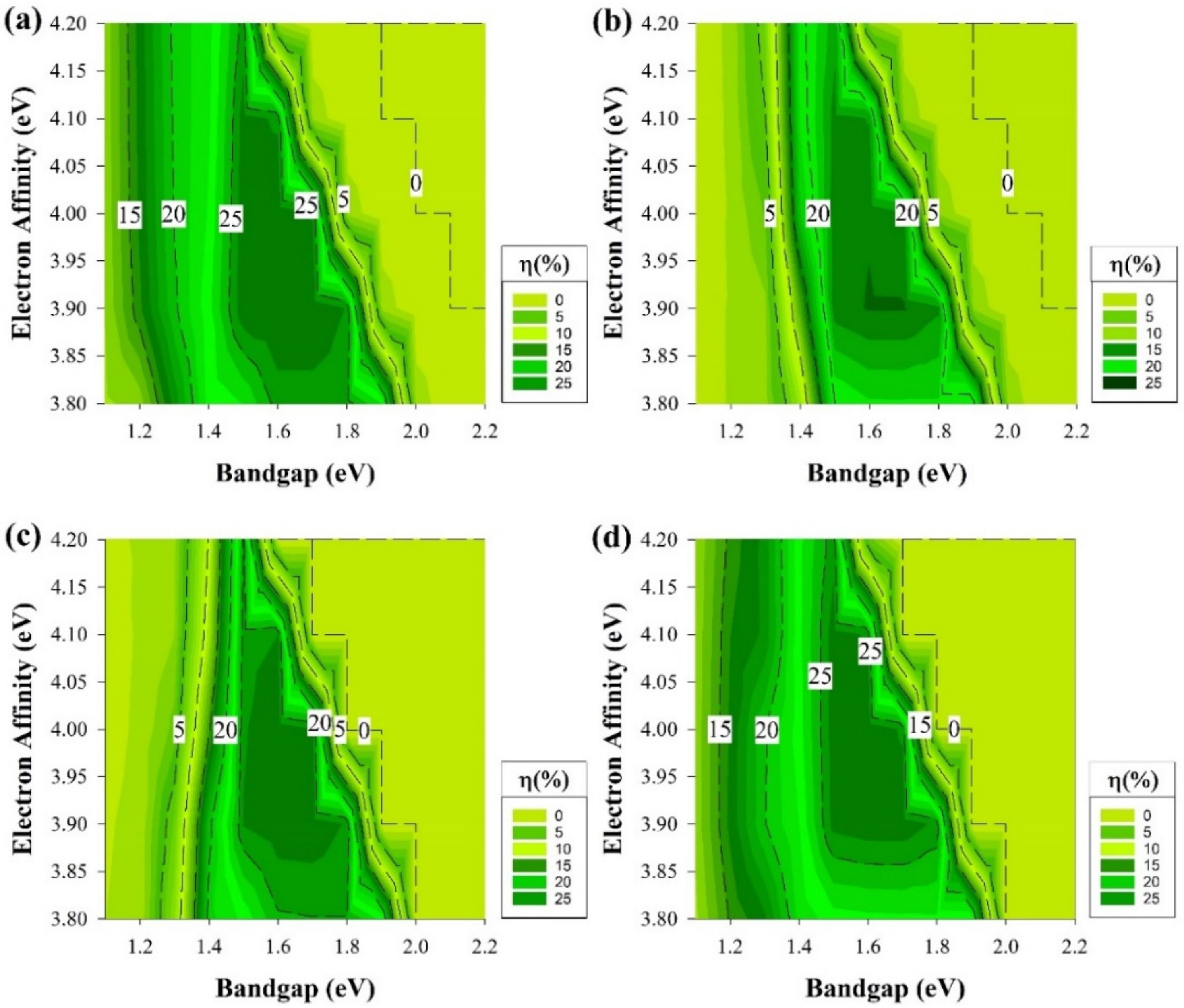
3.3. Non-Ideal State including Deep Level Defects

As our study advances to the next step of adding defects with the same conditions as the previous part but to a different location as it will be in the middle of the Eg in this section, and the results are shown in Figure 9. It is clear at this point that the far-right side of each graph would remain as a dead zone. However, the deep defects showed a greater impact on all of the structures and shrinking the highest PCE regions and the overall active areas.
Deep defects have higher ionization energy. Thus, these contribute very little to the free charge carriers. Defects with deep levels in the Eg are often referred to as traps, recombination centers, or generation centers. Figure 3a,d, which represent the front emitter structure, still shows the same trend, while the rear emitter structures have a similar trend as well. These results indicate that mid-gap defects have a lesser impact on front emitter cells compared to the rear emitter.
Figure 10 depicts the results of applying defects at the middle of the Eg while having the ideal i-a-Si:H layer. The n-type silicon wafer still shows similar performance to the cells with defects near the EV, while the p-type cells here illustrate a reduction in the performance at the region above χ 4.05 eV in Eg between 1.3 to 1.5 eV and 1.7 to 2 eV. Various recombination behaviors are usually caused by the band offsets asymmetry in n and p-type silicon heterojunction cells.
The dangling bond defect density goes up when the Fermi level is pushed closer to the EV edge. In n-type wafers, holes are considered as the minority carriers, in that case, a greater valance band offset is beneficial since it reduces the possibility of the interfacial recombination happening. On the other hand, a lesser ∆EC is undesirable for p-type silicon heterojunction cells, since electrons are the minority carriers, as this would result in an increase of the interfacial recombination probability to occur [60].

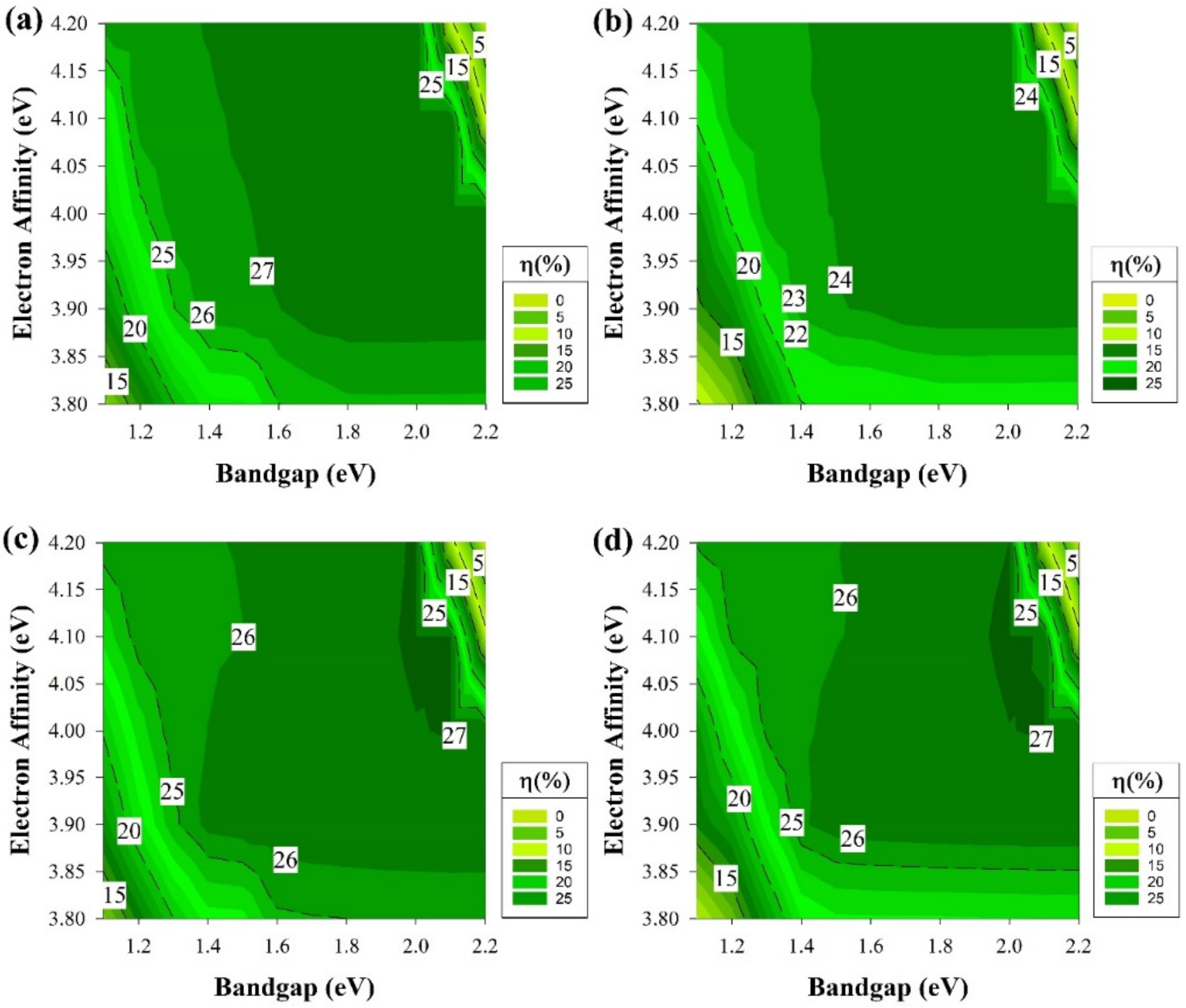
3.4. Non-Ideal State including Shallow Defects

Figure 11 and Figure 12 represent the last part of the study where the defects in this part are located near the Ec, exactly 0.2 eV below the Ec. The results in this part are very much the same as the results of the prior section addressing the deep defects. It is clear that the deep defects have a similar effect to the one near the Ec for both wafers, which is mainly due to the same reason, which influences the cell performance and causes the decay in certain regions of the graphs.
The shallow defects near Ev showed different behaviors in capturing the carriers and changing the device performance. These shallow defects sometimes could be the impurity elements used as dopants in semiconductors materials, which creates these shallow levels that become ionized at room temperature and provide free carriers. Yet, the region of a-Si:H layer parameter (Eg = 1.7 and χ = 3.9 eV) has always been the location of consistent performance. It yielded one of the highest efficiencies in each structure if not the highest in some of the cases mentioned above.
Growing an intrinsic a-Si:H layer on top of crystalline silicon reduces interface recombination efficiently with more symmetry as far as the passivation of different doping types and levels. Moreover, the n-type wafer has proven that it would work under any circumstances if the intrinsic layer is fabricated flawlessly. This indicates that the n-type wafers could perform better than p-type if they have a good passivation layer.

4. Conclusions

Numerical simulations of the front and rear-emitter HIT solar cells were investigated using AFORS-HET in this study. Both p- and n-type wafers were compared as a function of various Eg and χ for all passivating and doped layers in both ideal and non-ideal conditions. In ideal conditions, the p-type wafer with a front-emitter structure resulted in 28% of the maximum PCE, while the n-type wafer showed its maximum PCE of 26% from the rear-emitter. These high-performance devices yielded from the optimum regions, while the Eg and χ for all passivating and doping layers were at 1.3 to 1.7 eV and 3.9 to 4 eV, respectively.
To achieve similar performance at higher χ (e.g., 4 to 4.2 eV), the Eg should be between 1.3 and 1.5 eV. This trend was similar in rear and front-emitter structures using p- and n-type wafers; however, the performance decreased slightly. We found that a-Si:H buffer layers may couple well with doping layers with the Eg from 1.3 to 2 eV and 1.8 to 2 eV for front and rear-emitter structures regardless of the type of wafers. However, the front and rear-emitter structures still provided higher efficiencies for p- and n-types.
In non-ideal conditions, the effects of defects on passivating and doping layers led to the optimum regions being limited. We found that p-type devices produced a similar performance for both front and rear-emitter structures assuming that the levels of the defects remained at the middle or close to the Ec for all passivating and doped layers. This observation validates the advantages of using p-type wafers in this scenario. In contrast, the insertion of a-Si:H as passivating layers brings significant advantages to n-type wafers by widening the optimum region. Finally, these observations were successfully correlated with the band offsets and the illumination reduction by the a-Si:H layer at the emitter side.

Author Contributions

Data curation, S.A.S., I.S.M. and P.C.; Funding acquisition, N.A. and T.S.K.; Investigation, W.M.A. and I.S.M.; Methodology, S.A.S.; Resources, N.A. and T.S.K.; Software, W.M.A. and I.S.M.; Supervision, N.A. and A.A.A.; Validation, S.A.S., A.A.A. and P.C.; Visualization, W.M.A.; Writing—original draft, W.M.A.; Writing—review & editing, S.A.S. and P.C. All authors have read and agreed to the published version of the manuscript.

Funding

The authors wish to thank the Ministry of Higher Education of Malaysia (MoHE) for providing the research grant with the code of FRGS/1/2018/STG07/UNITEN/01/2 for this work. Due appreciation is also credited to the iRMC of the Universiti Tenaga Nasional (@The National Energy University) for the support through BOLD2025 Program.

Institutional Review Board Statement

Not applicable.

Informed Consent Statement

Not applicable.

Data Availability Statement

The data presented in this study are available upon request from the corresponding author.

Conflicts of Interest

The authors declare no conflict of interest.

References

  1. Fuhs, W.; Niemann, K.; Stuke, J. Heterojunctions of Amorphous Silicon and Silicon Single Crystals. In AIP Conference Proceedings; American Institute of Physics: College Park, MD, USA, 1974; Volume 20, pp. 345–350. [Google Scholar] [CrossRef]
  2. Hamakawa, Y.; Fujimoto, K.; Okuda, K.; Kashima, Y.; Nonomura, S.; Okamoto, H. New types of high efficiency solar cells based on a-Si. Appl. Phys. Lett. 1983, 43, 644–646. [Google Scholar] [CrossRef]
  3. Wakisaka, K.; Taguchi, M.; Sawada, T.; Tanaka, M.; Matsuyama, T.; Matsuoka, T.; Tsuda, S.; Nakano, S.; Kishi, Y.; Kuwano, Y. More than 16% solar cells with a new ‘HIT’ (doped a-Si/nondoped a-Si/crystalline Si) structure. In Proceedings of the The Conference Record of the Twenty-Second IEEE Photovoltaic Specialists Conference, Las Vegas, NV, USA, 7–11 October 1991; Volume 882, pp. 887–892. [Google Scholar]
  4. Zhang, Y.; Cong, R.; Zhao, W.; Li, Y.; Jin, C.; Yu, W.; Fu, G. Improved hetero-interface passivation by microcrystalline silicon oxide emitter in silicon heterojunction solar cells. Sci. Bull. 2016, 61, 787–793. [Google Scholar] [CrossRef] [Green Version]
  5. Wang, Q.; Page, M.R.; Iwaniczko, E.; Xu, Y.; Roybal, L.; Bauer, R.; To, B.; Yuan, H.-C.; Duda, A.; Hasoon, F.; et al. Efficient heterojunction solar cells on p-type crystal silicon wafers. Appl. Phys. Lett. 2010, 96, 013507. [Google Scholar] [CrossRef] [Green Version]
  6. De Wolf, S.; Descoeudres, A.; Holman, Z.C.; Ballif, C.J.G. High-efficiency silicon heterojunction solar cells: A review. Green 2012, 2, 7–24. [Google Scholar] [CrossRef]
  7. Bothe, K.; Schmidt, J. Electronically activated boron-oxygen-related recombination centers in crystalline silicon. J. Appl. Phys. 2006, 99, 013701. [Google Scholar] [CrossRef]
  8. Chavali, R.V.K.; De Wolf, S.; Alam, M.A. Device physics underlying silicon heterojunction and passivating-contact solar cells: A topical review. Prog. Photovolt. Res. Appl. 2018, 26, 241–260. [Google Scholar] [CrossRef]
  9. Hallam, B.J.; Hamer, P.G.; Wang, S.; Song, L.; Nampalli, N.; Abbott, M.D.; Chan, C.E.; Lu, D.; Wenham, A.M.; Mai, L.; et al. Advanced Hydrogenation of Dislocation Clusters and Boron-oxygen Defects in Silicon Solar Cells. Energy Procedia 2015, 77, 799–809. [Google Scholar] [CrossRef] [Green Version]
  10. Hallam, B.; Chen, D.; Kim, M.; Stefani, B.; Hoex, B.; Abbott, M.; Wenham, S. The role of hydrogenation and gettering in enhancing the efficiency of next-generation Si solar cells: An industrial perspective. Phys. Status Solidi (a) 2017, 214, 1700305. [Google Scholar] [CrossRef] [Green Version]
  11. Chen, D.; Weigand, W.; Wright, M.; Kim, M.; Shi, J.; Yu, Z.J.; Stefani, B.V.; Soeriyadi, A.; Holman, Z.; Hallam, B. Evaluating the Impact of and Solutions to Light-induced Degradation in Silicon Heterojunction Solar Cells. In Proceedings of the 2019 IEEE 46th Photovoltaic Specialists Conference (PVSC), Chicago, IL, USA, 16–21 June 2019; pp. 1099–1103. [Google Scholar]
  12. Herguth, A.; Schubert, G.; Kaes, M.; Hahn, G. A New Approach to Prevent the Negative Impact of the Metastable Defect in Boron Doped CZ Silicon Solar Cells. In Proceedings of the 2006 IEEE 4th World Conference on Photovoltaic Energy Conference, Waikoloa, HI, USA, 7–12 May 2006; pp. 940–943. [Google Scholar]
  13. Descoeudres, A.; Holman, Z.C.; Barraud, L.; Morel, S.; Wolf, S.D.; Ballif, C. >21% Efficient Silicon Heterojunction Solar Cells on n- and p-Type Wafers Compared. IEEE J. Photovolt. 2013, 3, 83–89. [Google Scholar] [CrossRef] [Green Version]
  14. Geilker, J.; Kwapil, W.; Rein, S. Light-induced degradation in compensated p- and n-type Czochralski silicon wafers. J. Appl. Phys. 2011, 109, 053718. [Google Scholar] [CrossRef]
  15. Schutz-Kuchly, T.; Dubois, S.; Veirman, J.; Veschetti, Y.; Heslinga, D.; Palais, O. Light-induced degradation in compensated n-type Czochralski silicon solar cells. Phys. Status Solidi 2011, 208, 572–575. [Google Scholar] [CrossRef]
  16. Descoeudres, A.; Horzel, J.; Paviet-Salomon, B.; Senaud, L.-L.; Christmann, G.; Geissbühler, J.; Wyss, P.; Badel, N.; Schüttauf, J.-W.; Zhao, J.; et al. The versatility of passivating carrier-selective silicon thin films for diverse high-efficiency screen-printed heterojunction-based solar cells. Prog. Photovolt. Res. Appl. 2020, 28, 569–577. [Google Scholar] [CrossRef]
  17. Philipps, S.; Warmuth, W. Fraunhofer ISE: Photovoltaics Report. Updated: 16 September 2020. Available online: https://www.ise.fraunhofer.de/en/publications/studies/photovoltaics-report.html (accessed on 10 February 2022).
  18. Allen, T.G.; Bullock, J.; Yang, X.; Javey, A.; De Wolf, S. Passivating contacts for crystalline silicon solar cells. Nat. Energy 2019, 4, 914–928. [Google Scholar] [CrossRef]
  19. The International Technology Roadmap for Photovoltaic (ITRPV). 2020. Available online: https://www.vdma.org/international-technology-roadmap-photovoltaic (accessed on 10 February 2022).
  20. Adachi, D.; Hernández, J.L.; Yamamoto, K. Impact of carrier recombination on fill factor for large area heterojunction crystalline silicon solar cell with 25.1% efficiency. Appl. Phys. Lett. 2015, 107, 233506. [Google Scholar] [CrossRef]
  21. Damon-Lacoste, J.; Cabarrocas, P.R.I. Toward a better physical understanding of a-Si:H/c-Si heterojunction solar cells. J. Appl. Phys. 2009, 105, 063712. [Google Scholar] [CrossRef]
  22. Tucci, M.; de Cesare, G. 17% efficiency heterostructure solar cell based on p-type crystalline silicon. J. Non-Cryst. Solids 2004, 338–340, 663–667. [Google Scholar] [CrossRef]
  23. Korte, L.; Conrad, E.; Angermann, H.; Stangl, R.; Schmidt, M. Advances in a-Si:H/c-Si heterojunction solar cell fabrication and characterization. Sol. Energy Mater. Sol. Cells 2009, 93, 905–910. [Google Scholar] [CrossRef]
  24. Maydell, K.V.; Conrad, E.; Schmidt, M. Efficient silicon heterojunction solar cells based on p- and n-type substrates processed at temperatures <220 °C. Curr. Org. Chem. 2006, 14, 289–295. [Google Scholar] [CrossRef]
  25. Miyajima, S.; Irikawa, J.; Yamada, A.; Konagai, M. High-quality nanocrystalline cubic silicon carbide emitter for crystalline silicon heterojunction solar cells. Appl. Phys. Lett. 2010, 97, 023504. [Google Scholar] [CrossRef]
  26. Ru, X.; Qu, M.; Wang, J.; Ruan, T.; Yang, M.; Peng, F.; Long, W.; Zheng, K.; Yan, H.; Xu, X. 25.11% efficiency silicon heterojunction solar cell with low deposition rate intrinsic amorphous silicon buffer layers. Sol. Energy Mater. Sol. Cells 2020, 215, 110643. [Google Scholar] [CrossRef]
  27. Pysch, D.; Bivour, M.; Hermle, M.; Glunz, S.W. Amorphous silicon carbide heterojunction solar cells on p-type substrates. Thin Solid Film. 2011, 519, 2550–2554. [Google Scholar] [CrossRef]
  28. Bhattacharya, S.; John, S. Beyond 30% Conversion Efficiency in Silicon Solar Cells: A Numerical Demonstration. Sci. Rep. 2019, 9, 12482. [Google Scholar] [CrossRef] [PubMed]
  29. Hasanah, L.; Ashidiq, A.; Pawinanto, R.E.; Mulyanti, B.; Wulandari, C.; Wiendartun, C.; Zain, A.R. Dimensional Optimization of TiO2 Nanodisk Photonic Crystals on Lead Iodide (MAPbI3) Perovskite Solar Cells by Using FDTD Simulations. Appl. Sci. 2022, 12, 351. [Google Scholar] [CrossRef]
  30. Yoo, J.J.; Seo, G.; Chua, M.R.; Park, T.G.; Lu, Y.; Rotermund, F.; Kim, Y.-K.; Moon, C.S.; Jeon, N.J.; Correa-Baena, J.-P.; et al. Efficient perovskite solar cells via improved carrier management. Nature 2021, 590, 587–593. [Google Scholar] [CrossRef]
  31. Meng, L.; You, J.; Yang, Y. Addressing the stability issue of perovskite solar cells for commercial applications. Nat. Commun. 2018, 9, 5265. [Google Scholar] [CrossRef] [PubMed]
  32. Mazzarella, L.; Kirner, S.; Stannowski, B.; Korte, L.; Rech, B.; Schlatmann, R. p-type microcrystalline silicon oxide emitter for silicon heterojunction solar cells allowing current densities above 40 mA/cm2. Appl. Phys. Lett. 2015, 106, 023902. [Google Scholar] [CrossRef]
  33. Demaurex, B.; Wolf, S.D.; Descoeudres, A.; Holman, Z.C.; Ballif, C. Damage at hydrogenated amorphous/crystalline silicon interfaces by indium tin oxide overlayer sputtering. Appl. Phys. Lett. 2012, 101, 171604. [Google Scholar] [CrossRef] [Green Version]
  34. Liu, W.; Zhang, L.; Cong, S.; Chen, R.; Wu, Z.; Meng, F.; Shi, Q.; Liu, Z. Controllable a-Si:H/c-Si interface passivation by residual SiH4 molecules in H2 plasma. Sol. Energy Mater. Sol. Cells 2018, 174, 233–239. [Google Scholar] [CrossRef]
  35. Deligiannis, D.; Vliet, J.v.; Vasudevan, R.; Swaaij, R.A.C.M.M.v.; Zeman, M. Passivation mechanism in silicon heterojunction solar cells with intrinsic hydrogenated amorphous silicon oxide layers. J. Appl. Phys. 2017, 121, 085306. [Google Scholar] [CrossRef]
  36. Tohoda, S.; Fujishima, D.; Yano, A.; Ogane, A.; Matsuyama, K.; Nakamura, Y.; Tokuoka, N.; Kanno, H.; Kinoshita, T.; Sakata, H.; et al. Future directions for higher-efficiency HIT solar cells using a Thin Silicon Wafer. J. Non-Cryst. Solids 2012, 358, 2219–2222. [Google Scholar] [CrossRef]
  37. Park, H.; Quddamah Khokhar, M.; Cho, E.-C.; Ju, M.; Kim, Y.; Kim, S.; Yi, J. Computer modeling of the front surface field layer on the performance of the rear-emitter silicon heterojunction solar cell with 25% efficiency. Optik 2020, 205, 164011. [Google Scholar] [CrossRef]
  38. Delavaran, H.; Shahhoseini, A. Hydrogenated Fluorinated Microcrystalline Silicon Oxide (µc-SiO:F:H):A New Material for the Emitter Layer of HIT Solar cells. In Proceedings of the 2019 27th Iranian Conference on Electrical Engineering (ICEE), Yazd, Iran, 30 April–2 May 2019; pp. 36–40. [Google Scholar]
  39. Fujiwara, H.; Kondo, M. Effects of a-Si:H layer thicknesses on the performance of a-Si:H∕c-Si heterojunction solar cells. J. Appl. Phys. 2007, 101, 054516. [Google Scholar] [CrossRef]
  40. Liu, J.; Huang, S.; He, L. Simulation of a high-efficiency silicon-based heterojunction solar cell. J. Semicond. 2015, 36, 044010. [Google Scholar] [CrossRef]
  41. Nunomura, S.; Sakata, I.; Matsubara, K. In-situ detection of interface defects in a-Si:H/c-Si heterojunction during plasma processing. Appl. Phys. Express 2019, 12, 051006. [Google Scholar] [CrossRef]
  42. Varache, R.; Leendertz, C.; Gueunier-Farret, M.E.; Haschke, J.; Muñoz, D.; Korte, L. Investigation of selective junctions using a newly developed tunnel current model for solar cell applications. Sol. Energy Mater. Sol. Cells 2015, 141, 14–23. [Google Scholar] [CrossRef]
  43. Street, R.A. Doping and the Fermi Energy in Amorphous Silicon. Phys. Rev. Lett. 1982, 49, 1187–1190. [Google Scholar] [CrossRef]
  44. Gaspari, F.; Quaranta, S. 2.5 PV Materials. In Comprehensive Energy Systems; Dincer, I., Ed.; Elsevier: Oxford, UK, 2018; pp. 117–149. [Google Scholar]
  45. Gaspari, F.; O’Leary, S.K.; Zukotynski, S.; Perz, J.M. The dependence of the dark conductivity of hydrogenated amorphous silicon films on the hydride content. J. Non-Cryst. Solids 1993, 155, 149–154. [Google Scholar] [CrossRef]
  46. Zhu, F.; Singh, J. Approach to study the relation between optical energy gap and hydrogen concentration in hydrogenated amorphous silicon thin films. J. Appl. Phys. 1993, 73, 4709–4711. [Google Scholar] [CrossRef]
  47. Green, M.; Dunlop, E.; Hohl-Ebinger, J.; Yoshita, M.; Kopidakis, N.; Hao, X. Solar cell efficiency tables (version 57). Prog. Photovoltaics Res. Appl. 2021, 29, 3–15. [Google Scholar] [CrossRef]
  48. Vallat-Sauvain, E.; Kroll, U.; Meier, J.; Shah, A.; Pohl, J. Evolution of the microstructure in microcrystalline silicon prepared by very high frequency glow-discharge using hydrogen dilution. J. Appl. Phys. 2000, 87, 3137–3142. [Google Scholar] [CrossRef] [Green Version]
  49. Holman, Z.C.; Descoeudres, A.; Barraud, L.; Fernandez, F.Z.; Seif, J.P.; Wolf, S.D.; Ballif, C. Current Losses at the Front of Silicon Heterojunction Solar Cells. IEEE J. Photovolt. 2012, 2, 7–15. [Google Scholar] [CrossRef] [Green Version]
  50. Nubile, P. Bandgap narrowing effects on the open circuit voltage in Si, GaAs and InP solar cells. Solid-State Electron. 1995, 38, 139–142. [Google Scholar] [CrossRef]
  51. Kraut, E.A. The effect of a valence-band offset on potential and current distributions in HgCdTe heterostructures. Vac. Sci. Technol. A Vacuum Surf. Films 1989, 7, 420–423. [Google Scholar] [CrossRef]
  52. Hussain, B.; Aslam, A.; Khan, T.M.; Creighton, M.; Zohuri, B. Electron Affinity and Bandgap Optimization of Zinc Oxide for Improved Performance of ZnO/Si Heterojunction Solar Cell Using PC1D Simulations. Electronics 2019, 8, 238. [Google Scholar] [CrossRef] [Green Version]
  53. Green, M.A. Solar cell fill factors: General graph and empirical expressions. Solid-State Electron. 1981, 24, 788–789. [Google Scholar] [CrossRef]
  54. Korte, L.; Schmidt, M. Doping type and thickness dependence of band offsets at the amorphous/crystalline silicon heterojunction. J. Appl. Phys. 2011, 109, 063714. [Google Scholar] [CrossRef]
  55. Fuhs, W.; Korte, L.; Schmidt, M.J.J.O.O.; Materials, A. Heterojunctions of hydrogenated amorphous silicon and monocrystalline silicon. J. Optoelectron. Adv. Mater. 2006, 8, 1989–1995. [Google Scholar]
  56. Schulze, T.F.; Korte, L.; Ruske, F.; Rech, B. Band lineup in amorphous/crystalline silicon heterojunctions and the impact of hydrogen microstructure and topological disorder. Phys. Rev. B 2011, 83, 165314. [Google Scholar] [CrossRef]
  57. Fonash, S. Solar Cell Device Physics; Elsevier: Oxford, UK, 2012. [Google Scholar]
  58. Ferdaous, M.T.; Shahahmadi, S.A.; Chelvanathan, P.; Akhtaruzzaman, M.; Alharbi, F.H.; Sopian, K.; Tiong, S.K.; Amin, N. Elucidating the role of interfacial MoS2 layer in Cu2ZnSnS4 thin film solar cells by numerical analysis. Sol. Energy 2019, 178, 162–172. [Google Scholar] [CrossRef]
  59. Weiss, T.P.; Bissig, B.; Feurer, T.; Carron, R.; Buecheler, S.; Tiwari, A.N. Bulk and surface recombination properties in thin film semiconductors with different surface treatments from time-resolved photoluminescence measurements. Sci. Rep. 2019, 9, 5385. [Google Scholar] [CrossRef] [Green Version]
  60. Chang, N.L.; Wright, M.; Egan, R.; Hallam, B. The Technical and Economic Viability of Replacing n-type with p-type Wafers for Silicon Heterojunction Solar Cells. Cell Rep. Phys. Sci. 2020, 1, 100069. [Google Scholar] [CrossRef]
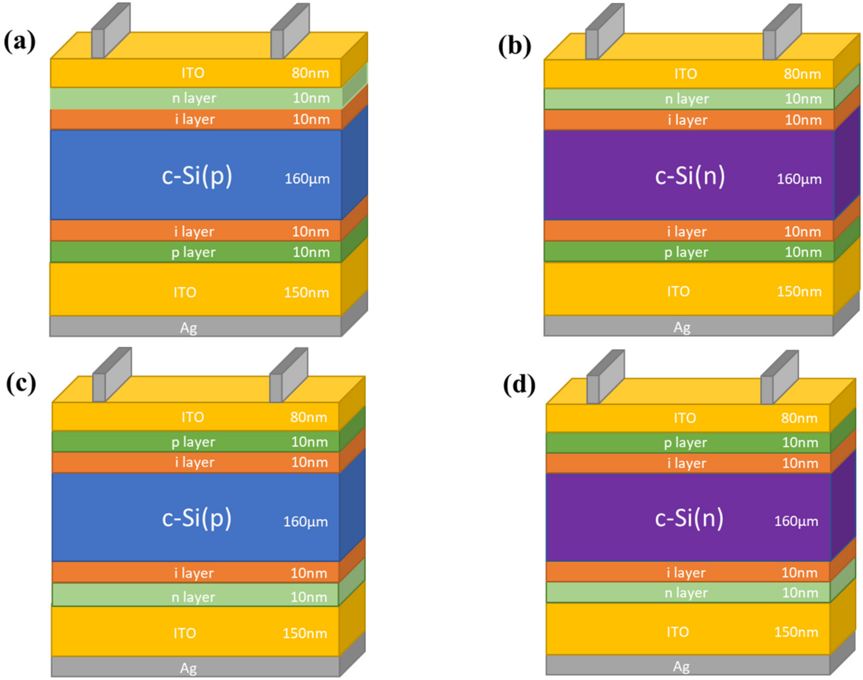
Figure 1. Schematic structure of HIT solar cells. (a) p-Type wafer with n-i-p structure (front-emitter cell). (b) n-Type wafer with n-i-p structure (front-emitter cell). (c) p-Type wafer with p-i-n structure (rear-emitter cell). (d) n-Type wafer with p-i-n structure (rear-emitter cell).
Materials 15 03508 g001
Figure 2. (ac) Defect state distributions in a-Si layers.
Materials 15 03508 g002
Figure 3. The efficiency of four proposed structures as a function of Eg and χ for all passivating and doped layers without defects. (a) Contour graphs of the n-i-p structure with p-type wafer base. (b) Contour graphs of the n-i-p structure with n-type wafer base. (c) Contour graphs of the p-i-n structure with the p-type wafer. (d) Contour graphs of the p-i-n structure with n-type wafer base.
Materials 15 03508 g003
Figure 4. Performance parameters of the structure in Figure 1a.
Materials 15 03508 g004
Figure 5. (a) The corresponding band diagram of structure p-i-n with p-type wafer when Eg = 1.1 and χ = 4. (b) The corresponding band diagram of structure n-i-p when Eg = 1.7 and χ = 3.9.
Materials 15 03508 g005
Figure 6. The efficiency of four proposed structures, including a-Si:H passivating layers as a function of Eg and χ for all doped layers without defects. (a) Contour graphs of the n-i-p structure with p-type wafer base. (b) Contour graphs of the n-i-p structure with n-type wafer base. (c) Contour graphs of the p-i-n structure with the p-type wafer. (d) Contour graphs of the p-i-n structure with n-type wafer base.
Materials 15 03508 g006
Figure 7. The efficiency of four proposed structures as a function of Eg and χ for all passivating and doped layers, including defects at the 0.2 eV level above the EV. (a) Contour graphs of the n-i-p structure with p-type wafer base. (b) Contour graphs of the n-i-p structure with n-type wafer base. (c) Contour graphs of the p-i-n structure with the p-type wafer. (d) Contour graphs of the p-i-n structure with n-type wafer base.
Materials 15 03508 g007
Figure 8. The efficiency of four proposed structures, including a-Si:H passivating layers as a function of Eg and χ for doped layers with defects at the 0.2 eV level above EV. (a) Contour graphs of the n-i-p structure with p-type wafer base. (b) Contour graphs of the n-i-p structure with n-type wafer base. (c) Contour graphs of the p-i-n structure with the p-type wafer. (d) Contour graphs of the p-i-n structure with n-type wafer base.
Materials 15 03508 g008
Figure 9. The efficiency of four proposed structures as a function of Eg and χ for all passivating and doped layers, including defects at the middle of Eg (a) Contour graphs of the n-i-p structure with p-type wafer base. (b) Contour graphs of the n-i-p structure with n-type wafer base. (c) Contour graphs of the p-i-n structure with the p-type wafer. (d) Contour graphs of the p-i-n structure with n-type wafer base.
Materials 15 03508 g009
Figure 10. The efficiency of four proposed structures, including a-Si:H passivating layers as a function of Eg and χ for doped layers with defects at the middle of Eg (a) Contour graphs of the n-i-p structure with p-type wafer base. (b) Contour graphs of the n-i-p structure with n-type wafer base. (c) Contour graphs of the p-i-n structure with the p-type wafer. (d) Contour graphs of the p-i-n structure with n-type wafer base.
Materials 15 03508 g010
Figure 11. The efficiency of four proposed structures as a function of Eg and χ for all passivating and doped layers, including defects at the 0.2 eV level below Ec. (a) Contour graphs of the n-i-p structure with p-type wafer base. (b) Contour graphs of the n-i-p structure with n-type wafer base. (c) Contour graphs of the p-i-n structure with the p-type wafer. (d) Contour graphs of the p-i-n structure with n-type wafer base. (ad) All graphs show the efficiency performance while varying the Eg and χ.
Materials 15 03508 g011
Figure 12. The efficiency of four proposed structures, including a-Si:H passivating layers as a function of Eg and χ for doped layers with defects at the 0.2 eV level below Ec. (a) Contour graphs of the n-i-p structure with p-type wafer base. (b) Contour graphs of the n-i-p structure with n-type wafer base. (c) Contour graphs of the p-i-n structure with the p-type wafer. (d) Contour graphs of the p-i-n structure with n-type wafer base.
Materials 15 03508 g012
Table 1. Parameters used in the simulation.
Parametersc-p-Sic-n-Sii-Layerp-Layern-Layer
Layer thickness (nm)16 × 10416 × 104101010
Dielectric constant11.911.911.911.911.9
Electron affinity (eV)4.054.053.8–4.23.8–4.23.8–4.2
Band gap (eV)1.121.121.1–2.21.1–2.21.1–2.2
Effective conduction band density (cm−3)2.8 × 10192.8 × 10191 × 10201 × 10201 × 1020
Effective valence band density (cm−3)1.04 × 10191.04 × 10191 × 10201 × 10201 × 1020
Electron mobility (cm2 V−1 s−1)10411041202020
Hole mobility (cm2 V−1 s−1)418418555
Acceptor concentration (cm−3)2 × 1017001 × 10200
Donor concentration (cm−3)02 × 1017001 × 1020
Thermal velocity of electrons (cm s−1)1 × 1071 × 1071 × 1071 × 1071 × 107
Thermal velocity of holes (cm s−1)1 × 1071 × 1071 × 1071 × 1071 × 107
Layer density (g cm−3)2.3282.3282.3282.3282.328
Auger recombination coefficient for electron (cm6 s−1)2.2 × 10−312.2 × 10−31000
Auger recombination coefficient for hole (cm6 s−1)9.9 × 10−329.9 × 10−32000
Direct band-to-band recombination coefficient (cm3 s−1)00000
Position of oxygen defectEV + 0.55EV + 0.55---
Density of states (cm−3 eV−1)1 × 10102.5 × 109---
σeh) for single defect states1 × 10−14 (1 × 10⁻¹⁴)1 × 10⁻¹⁴ (1 × 10⁻¹⁴)---
Table 2. Band diagram offset between i-a-Si/c-Si.
Conduction Band Offsetχ (eV)
3.83.944.14.2
ΔEc= χa−Si − χc−Si−0.25−0.15−0.050.050.15
Valence band offsetχ (eV)
3.83.944.14.2
Eg(eV)
1.1−0.27−0.17−0.070.030.13
1.2−0.17−0.070.030.130.23
1.3−0.070.030.130.230.33
1.40.030.130.230.330.43
1.50.130.230.330.430.53
1.60.230.330.430.530.63
1.70.330.430.530.630.73
1.80.430.530.630.730.83
1.90.530.630.730.830.93
20.630.730.830.931.03
2.10.730.830.931.031.13
2.20.830.931.031.131.23
Publisher’s Note: MDPI stays neutral with regard to jurisdictional claims in published maps and institutional affiliations.

