
Simulation and Optimization of FAPbI3 Perovskite Solar Cells with a BaTiO3 Layer for Efficiency Enhancement
 ,
,  , , and
Abstract
:1. Introduction
2. Materials and Methods
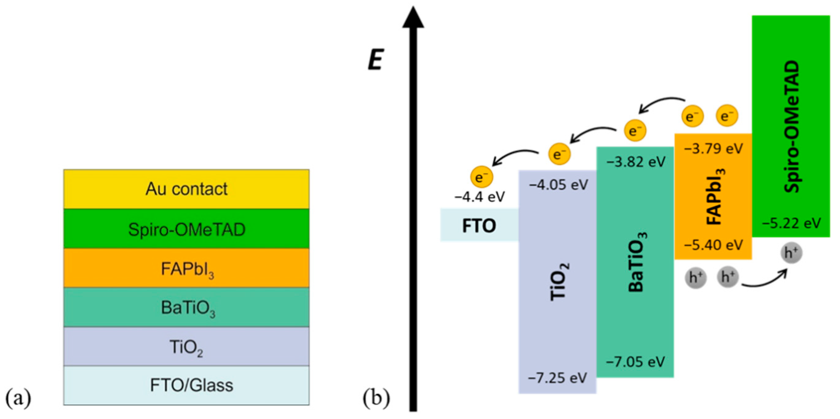
2.1. Preparation and Characterization of Perovskite Solar Cells
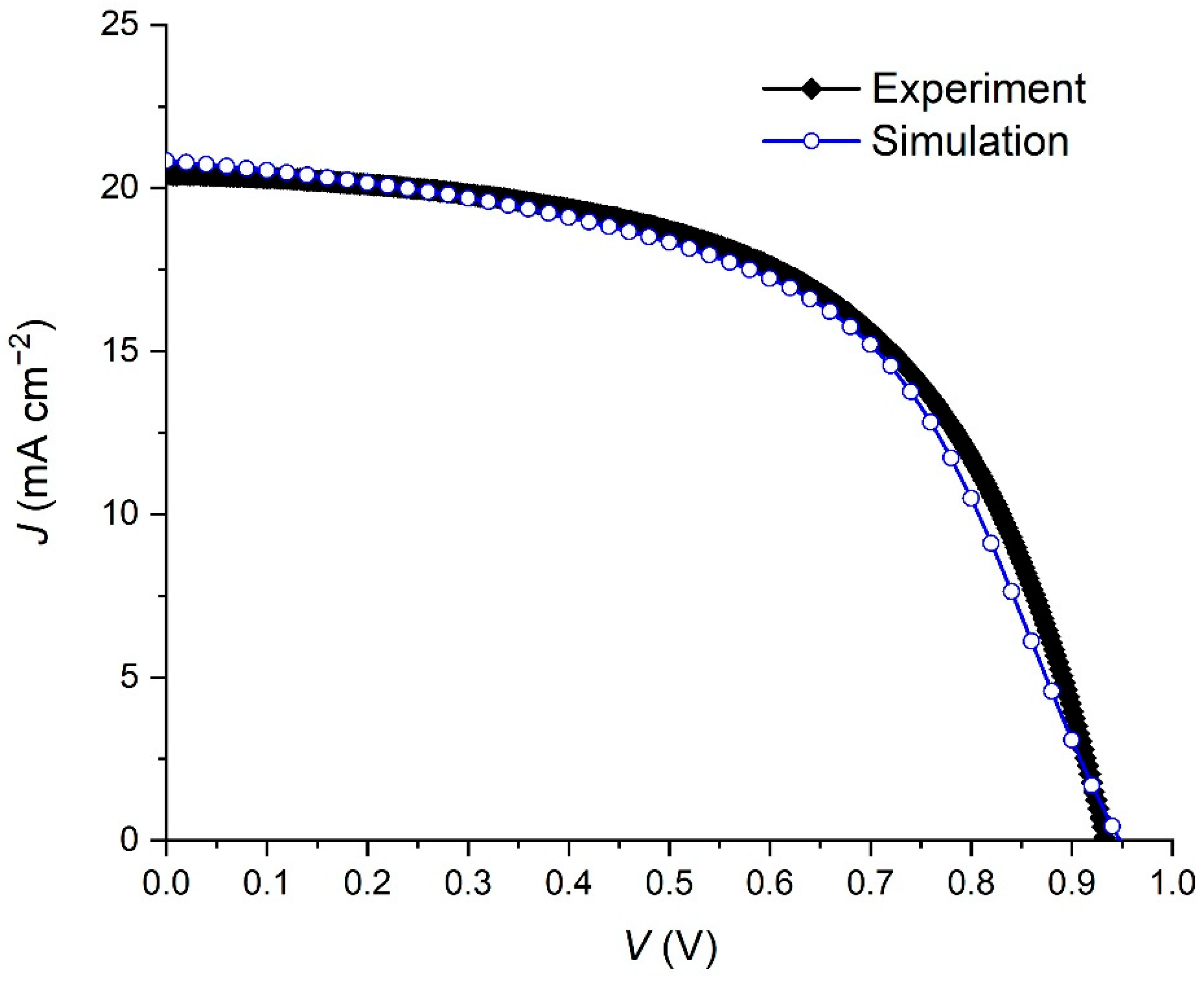
2.2. Numerical Simulation
3. Results and Discussion
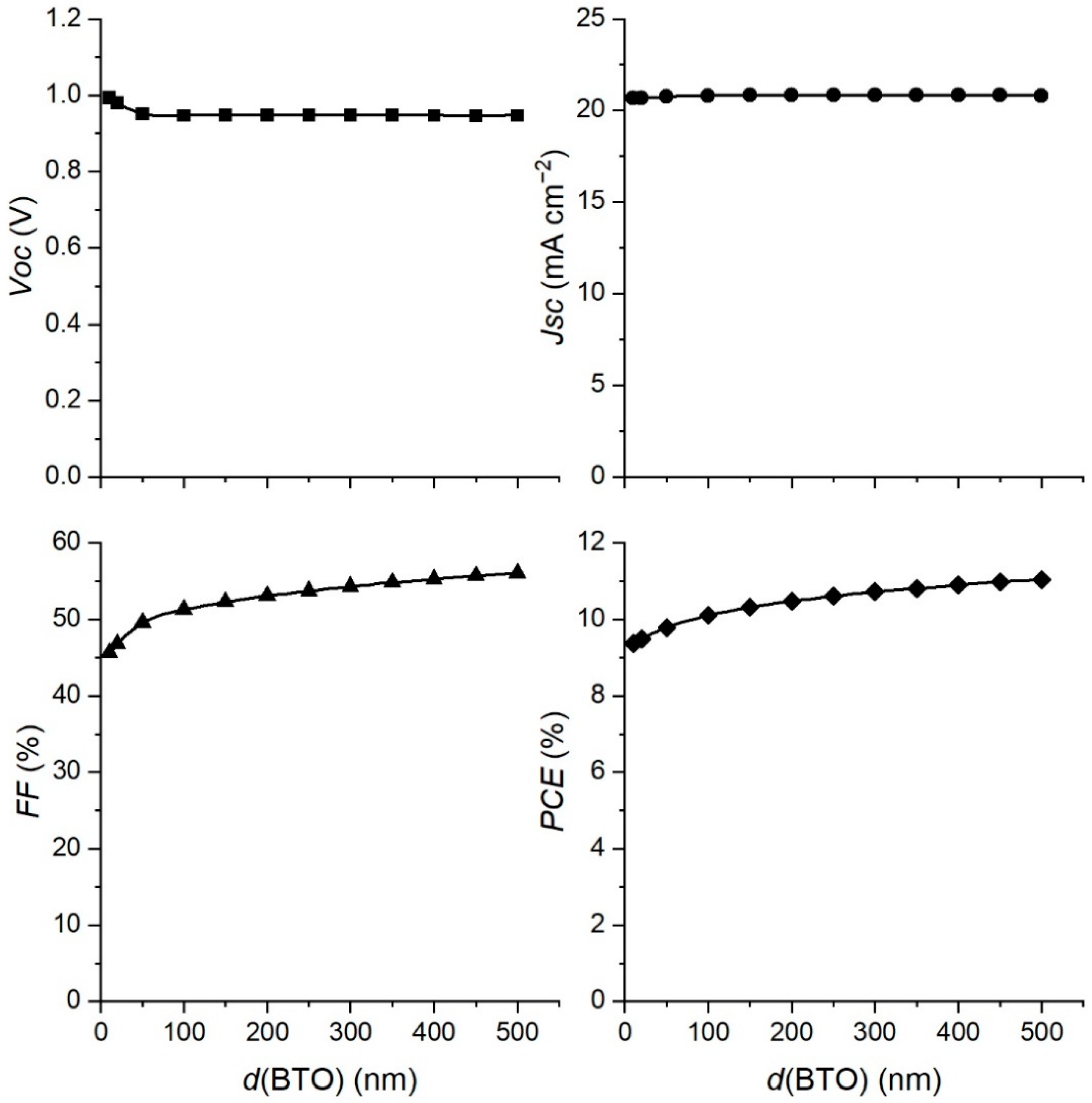
3.1. The Impact of the BaTiO3 Layer Thickness on the Performance of the PSC
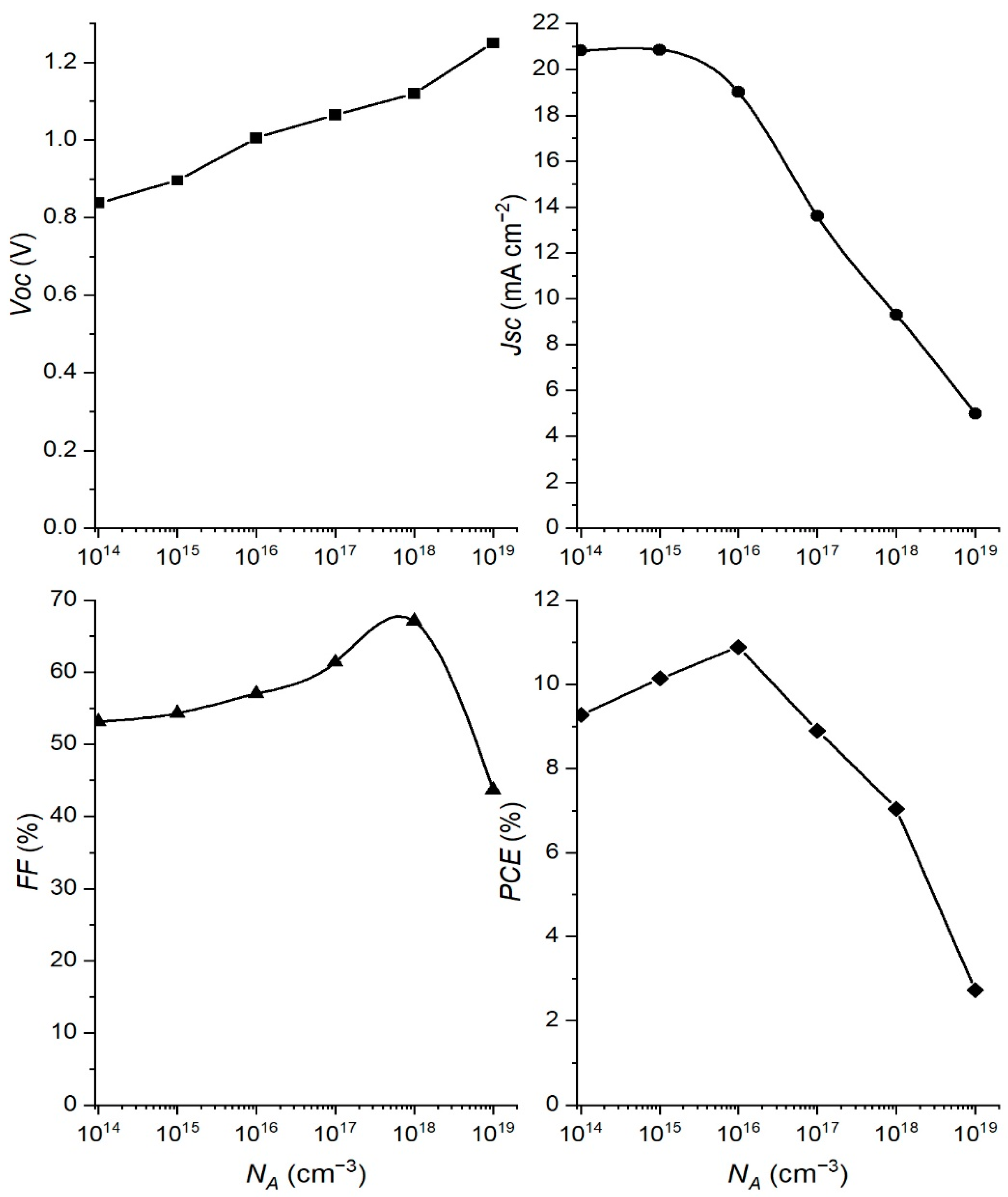
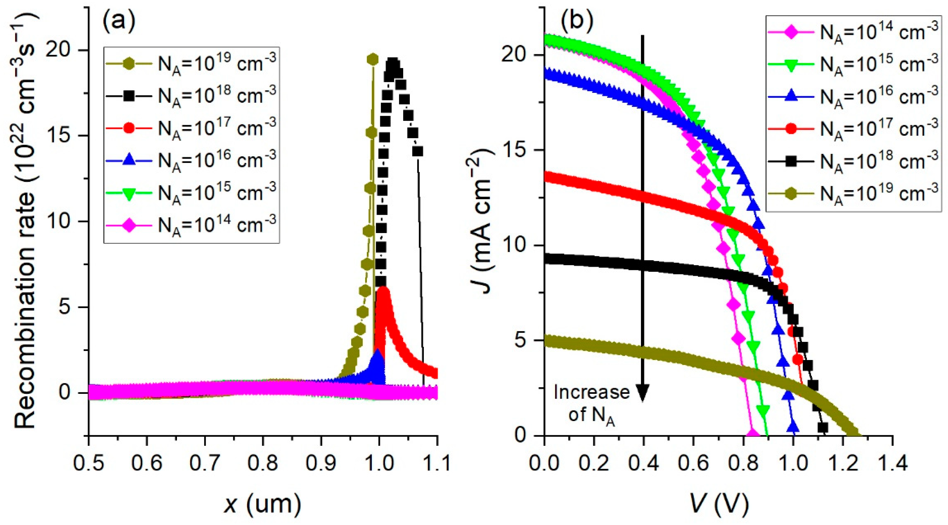
3.2. Effect of Changing the Absorber Doping Concentration
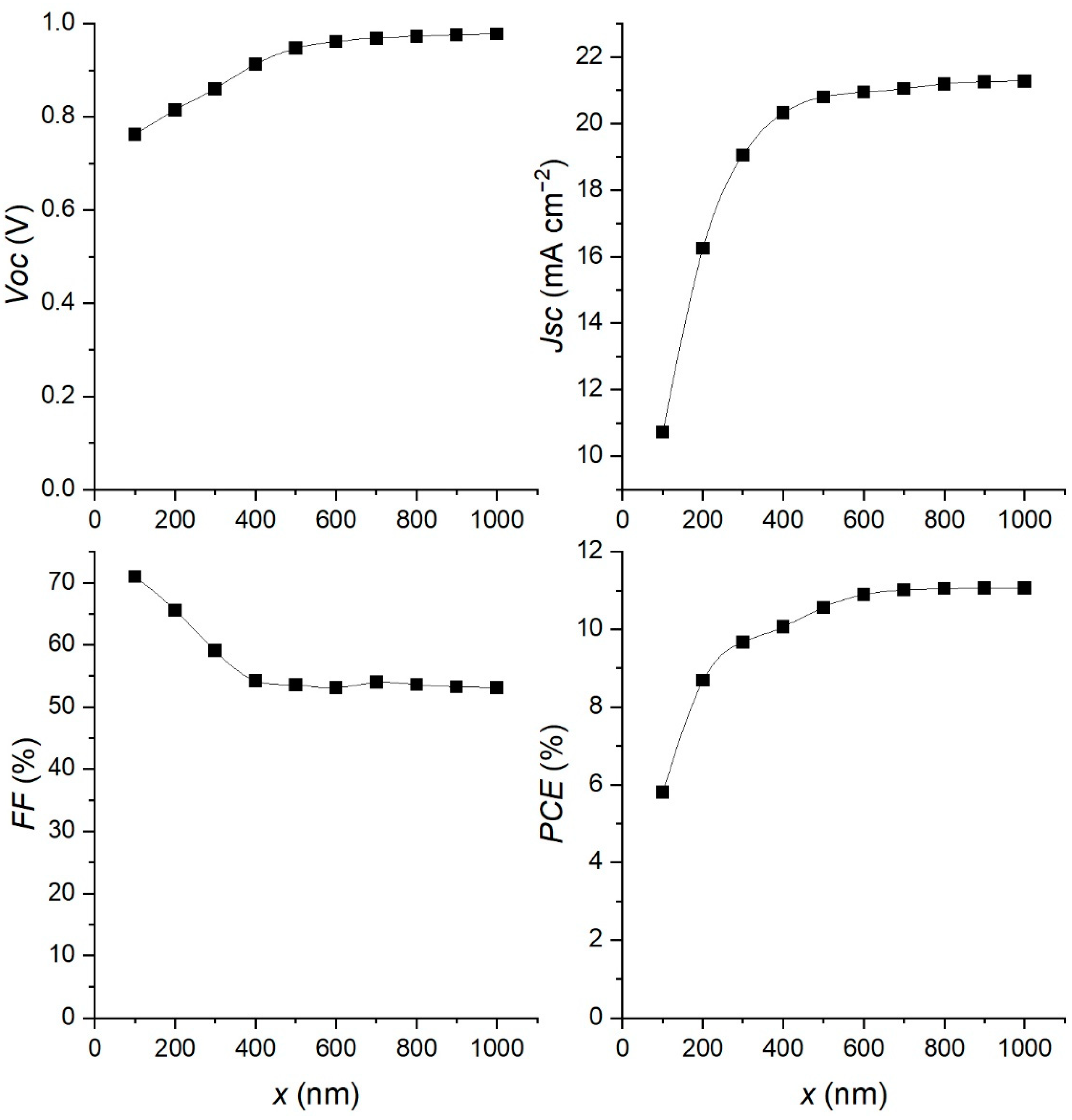
3.3. Effect of Changing Absorber Layer Thickness
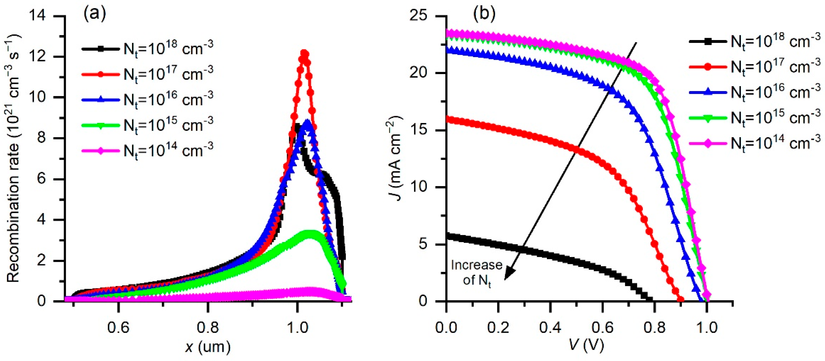
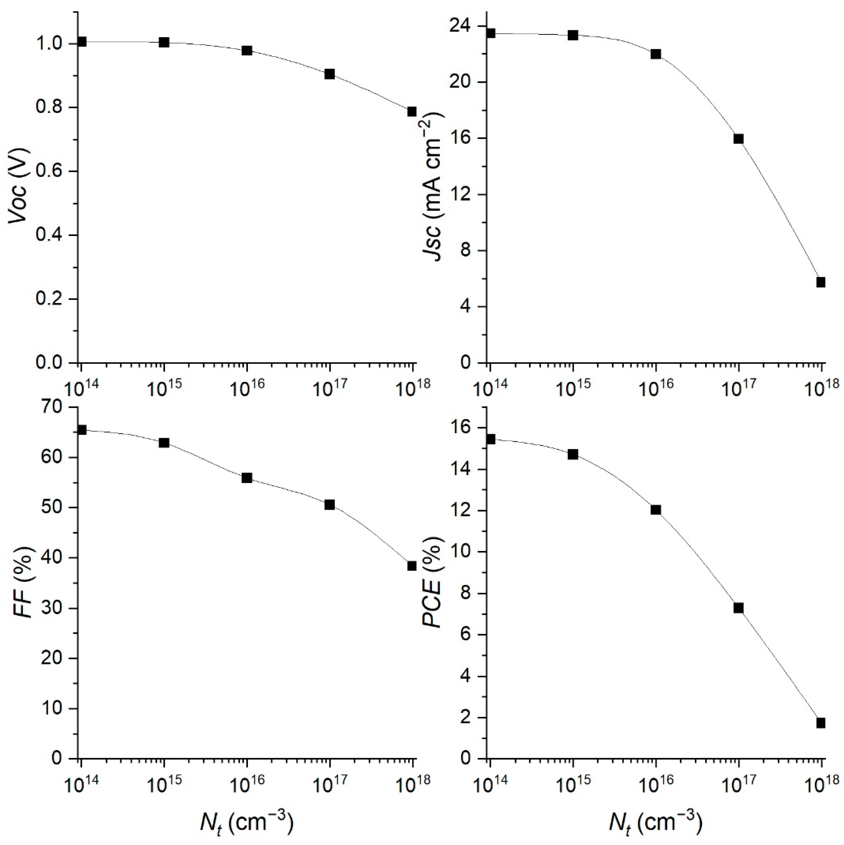
3.4. Effect of Changing the Defect Concentration Nt
4. Conclusions
Author Contributions
Funding
Institutional Review Board Statement
Informed Consent Statement
Data Availability Statement
Acknowledgments
Conflicts of Interest
References
- Eperon, G.E.; Stranks, S.D.; Menelaou, C.; Johnston, M.B.; Herz, L.M.; Snaith, H.J. Formamidinium lead trihalide: A broadly tunable perovskite for efficient planar heterojunction solar cells. Energy Environ. Sci. 2014, 7, 982–989. [Google Scholar] [CrossRef]
- Gelvez-Rueda, M.C.; Renaud, N.; Grozema, F.C. Temperature dependent charge carrier dynamics in formamidinium lead iodide perovskite. J. Phys. Chem. C 2017, 121, 23392–23397. [Google Scholar] [CrossRef] [PubMed]
- Belarbi, M.; Zeggai, O.; Louhibi-Fasla, S. Numerical study od methylammonium lead iodide perovskite solar cells using SCAPS-1D simulation program. Mater. Today 2022, 51, 2115–2119. [Google Scholar] [CrossRef]
- Doyranly, C.; Choi, F.P.G.; Alishah, H.M.; Koyuncu, S.; Gunes, S.; San, N. Triphenylamine-based organic small-molecule interlayer materials for inverted perovskite solar cells. Org. Electron. 2022, 188, 106595. [Google Scholar] [CrossRef]
- Deepthi Jayan, K. Design and comparative performance analysis of high-efficiency lead-based and lead-free perovskite solar cells. Phys. Status Solidi A 2022, 219, 2100606. [Google Scholar] [CrossRef]
- Karthick, S.; Velumani, S.; Bouclé, J. Chalcogenide BaZrS3 perovskite solar cells: A numerical simulation and analysis using SCAPS 1D. Opt. Mater. 2022, 126, 112250. [Google Scholar] [CrossRef]
- Okamoto, Y.; Suzuki, Y. Mesoporous BaTiO3/TiO2 double layer for electron transport in perovskite solar cells. J. Phys. Chem. C 2016, 120, 13995–14000. [Google Scholar] [CrossRef]
- Qin, J.; Zhang, Z.; Shi, W.; Liu, Y.; Gao, H.; Mao, Y. Enhanced performance of perovskite solar cells by using ultrathin BaTiO3 interface modification. ACS Appl. Mater. Interfaces 2018, 10, 36067–36074. [Google Scholar] [CrossRef]
- Zhang, J.; Meng, X.; Su, P.; Liu, L.; Feng, S.; Wang, J.; Liu, T.; Yang, J.; Yang, H.; Fu, W. Applying BaTiO3-coated TiO2 core–shell nanoparticles films as scaffold layers to optimize interfaces for better-performing perovskite solar cells. J. Mater. Sci. Mater. Electron. 2019, 30, 7733–7742. [Google Scholar] [CrossRef]
- Zhang, X.; Zhang, J.; Su, P.; Feng, S.; Xu, R.; Bian, C.; Fu, W.; Yang, H.; Li, Z. Perovskite-type BaTiO3 nanocrystal modifier in TiO2/CH3NH3PbI3 interface to enhance the performance of planar perovskite solar cells. J. Electron. Mater. 2020, 49, 4601–4609. [Google Scholar] [CrossRef]
- Stanić, D.; Kojić, V.; Čižmar, T.; Juraić, K.; Bagladi, L.; Mangalam, J.; Rath, T.; Gajović, A. Simulating the Performance of a Formamidinium Based Mixed Cation Lead Halide Perovskite Solar Cell. Materials 2021, 14, 6341. [Google Scholar] [CrossRef] [PubMed]
- Jafarzadeh, F.; Aghili, H.; Nikbakht, H.; Javadpour, S. Design and optimization of highly efficient perovskite/homojunction SnS tandem solar cells using SCAPS-1D. Sol. Energy 2022, 236, 195–205. [Google Scholar] [CrossRef]
- Kumar, P.; Shankar, G.; Pradhan, B. Improved performance study of monolithic all perovskite tandem solar cell in nip and pin structure. Mater. Taday Proc. 2022, in press. [Google Scholar] [CrossRef]
- Bal, S.S.; Basak, A.; Singh, U.P. Numerical modeling and performance analysis of Sb-based tandem solar cell structure using SCAPS-1D. Opt. Mater. 2022, 127, 112282. [Google Scholar] [CrossRef]
- Kim, T.; Lim, J.; Song, S. Recent progress and challenges of electron transport layers in organic–inorganic perovskite solar cells. Energies 2020, 13, 5572. [Google Scholar] [CrossRef]
- Burgelman, M.; Nollet, P.; Degrave, S. Modelling polycrystalline semiconductor solar cells. Thin Solid Film. 2000, 361, 527–532. [Google Scholar] [CrossRef]
- Karthick, S.; Velumani, S.; Bouclé, J. Experimental and SCAPS simulated formamidinium perovskite solar cells: A comparison of device performance. Sol. Energy 2020, 205, 349–357. [Google Scholar] [CrossRef]
- Abdelaziz, S.; Zekry, A.; Shaker, A.; Abouletta, M. Investigating the performance of formamidinium tin-based perovskite solar cell by SCAPS device simulation. Opt. Mater. 2020, 101, 109738. [Google Scholar] [CrossRef]
- Du, H.-J.; Wang, W.-C.; Zhu, J.-Z. Device simulation of lead-free CH3NH3SnI3 perovskite solar cells with high efficiency. Chin. Phys. B 2016, 25, 108802. [Google Scholar] [CrossRef]
- Stamate, M.D. On the dielectric properties of dc magnetron TiO2 thin films. Appl. Surf. Sci. 2003, 218, 318–323. [Google Scholar] [CrossRef]
- Saha, R.; Chakraborty, K.; Choudhury, M.G.; Paul, S. Simulation study of Formamidinium Lead Halide (FAPbX3; X = I and Br) Based Perovskite Solar Cells Using SCAPS-1D Device Simulator. J. Nano Electron. Phys. 2021, 13, 03019. [Google Scholar] [CrossRef]
- Suzuki, K.; Kijima, K. Optical Band Gap of Barium Titanate Nanoparticles Prepared by RF-plasma Chemical Vapor Deposition. Jpn. J. Appl. Phys. 2005, 44, 2081–2082. [Google Scholar] [CrossRef]
- Vagadia, M.; Ravalia, A.; Solanki, P.S.; Pandey, P.; Asokan, K.; Kuberkar, D.G. Electrical properties of BaTiO3 based—MFIS heterostructure: Role of semiconductor channel carrier concentration. AIP Adv. 2014, 4, 057131. [Google Scholar] [CrossRef]
- Yusoff, N.H.; Osman, R.A.M.; Idris, M.S.; Muhsen, K.N.D.K.; Nor, N.I.M. Dielectric and structural analysis of hexagonal and tetragonal phase BaTiO3. AIP Conf. Proc. 2020, 2203, 020038. [Google Scholar] [CrossRef]
- Chen, L.C.; Tseng, Z.L.; Huang, J.K. A study of inverted-type perovskite solar cells with various composition ratios of (FAPbI3)1-x(MAPbI3)x. Nanomaterials 2016, 6, 183. [Google Scholar] [CrossRef] [Green Version]
- Ma, F.; Li, J.; Li, W.; Lin, N.; Wang, L.; Qiao, J. Stable α/δ phase junction of formamidinium lead iodide perovskites for enhanced near-infrared emission. Chem. Sci. 2017, 8, 80. [Google Scholar] [CrossRef] [Green Version]
- Zhou, Y.; Long, G. Low density of conduction and valence band states contribute to the high open-circuit voltage in perovskite solar cells. J. Phys. Chem. C 2017, 121, 3. [Google Scholar] [CrossRef]
- Zhang, C.; Li, X.; Ding, L.; Jin, C.; Tao, H. Effect of BaTiO3 powder as an additive in perovskite films on solar cells. RSC Adv. 2022, 12, 7950. [Google Scholar] [CrossRef]
- Shi, J.; Wei, H.; Lv, S.; Xu, X.; Wu, H.; Luo, Y.; Li, D.; Meng, Q. Control of Charge Transport in the Perovskite CH3NH3PbI3 Thin Film. ChemPhysChem 2015, 16, 842–847. [Google Scholar] [CrossRef]
- Bi, C.; Shao, Y.; Yuan, Y.; Xiao, Z.; Wang, C.; Gao, Y.; Huang, J. Understanding the formation and evolution of interdiffusion grown organolead halide perovskite thin films by thermal annealing. J. Mater. Chem. A 2014, 2, 18508–18514. [Google Scholar] [CrossRef]
- Yin, J.; Cortecchia, D.; Krishna, A.; Chen, S.; Mathews, N.; Grimsdale, A.C.; Soci, C. Interfacial Charge Transfer Anisotropy in Polycrystalline Lead Iodide Perovskite Films. J. Phys. Chem. Lett. 2015, 6, 1396–1402. [Google Scholar] [CrossRef] [PubMed]
- Xing, G.C.; Mathews, N.; Sun, S.Y.; Lim, S.S.; Lam, Y.M.; Grätzel, M.; Mhaisalkar, S.; Sum, T.C. Long-Range Balanced Electronand Hole-Transport Lengths in Organic-Inorganic CH3NH3PbI3. Science 2013, 342, 344–347. [Google Scholar] [CrossRef] [PubMed]
- Hao, F.; Stoumpos, C.C.; Guo, P.; Zhou, N.; Marks, T.J.; Chang, R.P.H.; Kanatzidis, M.G. Solvent-Mediated Crystallization of CH3NH3SnI3 Films for Heterojunction Depleted Perovskite Solar Cells. J. Am. Chem. Soc. 2015, 137, 11445–11452. [Google Scholar] [CrossRef] [PubMed]
- Shockley, W.; Read, W.T.; Sze, S.M. Statistics of the Recombinations of Holes and Electrons. In Semiconductor Devices: Pioneering Papers; World Scientific: London, UK, 1991; pp. 62–69. [Google Scholar]
- Grove, A.S. Physics and Technology of Semiconductor Devices, 1st ed.; John Wiley and Sons: New York, NY, USA, 1967; pp. 129–133. [Google Scholar]


| Parameter | FTO [17,18] | TiO2 [11,18,19] | BaTiO3 | FAPbI3 [17] | spiro-OMeTAD [17,18,21] |
|---|---|---|---|---|---|
| Thickness (nm) | 300 * | 100 * | 300 * | 550 * | 500 * |
| Band gap (eV) | 3.5 | 3.26 | 3.2 [22] | 1.51 | 2.9 |
| Electron affinity (eV) | 4.0 | 4.2 | 3.8 [23] | 4.0 [25] | 2.2 |
| Dielectric permittivity | 9 | 9 [20] | 2500 [24] | 6.6 [26] | 3 |
| CB effective density of states (cm−3) | 2·1018 | 2.2·1018 | 2.2·1018 | 1.2·1019 [27] | 2.2·1018 |
| VB effective density of states (cm−3) | 1.8·1019 | 1.8·1018 | 1.8·1018 | 2.9·1018 [2] | 1.8·1018 |
| Thermal velocity of electrons (cm/s) | 107 | 107 | 107 | 107 | 107 |
| Thermal velocity of holes (cm/s) | 107 | 107 | 107 | 107 | 107 |
| Electron mobility (cm2/Vs) | 20 | 20 | 20 | 2.7 [2] | 10−4 |
| Hole mobility (cm2/Vs) | 10 | 10 | 10 | 1.8 [2] | 10−4 |
| Shallow donor density ND (cm−3) | 1019 | 5·1016 | 5·1016 | 0 | 0 |
| Shallow acceptor density NA (cm−3) | 0 | 0 | 0 | 1.9·1015 | 1018 |
| Defect density Nt (cm−3) | 1015 | 1015 | 1015 | 1.9·1016 | 1015 |
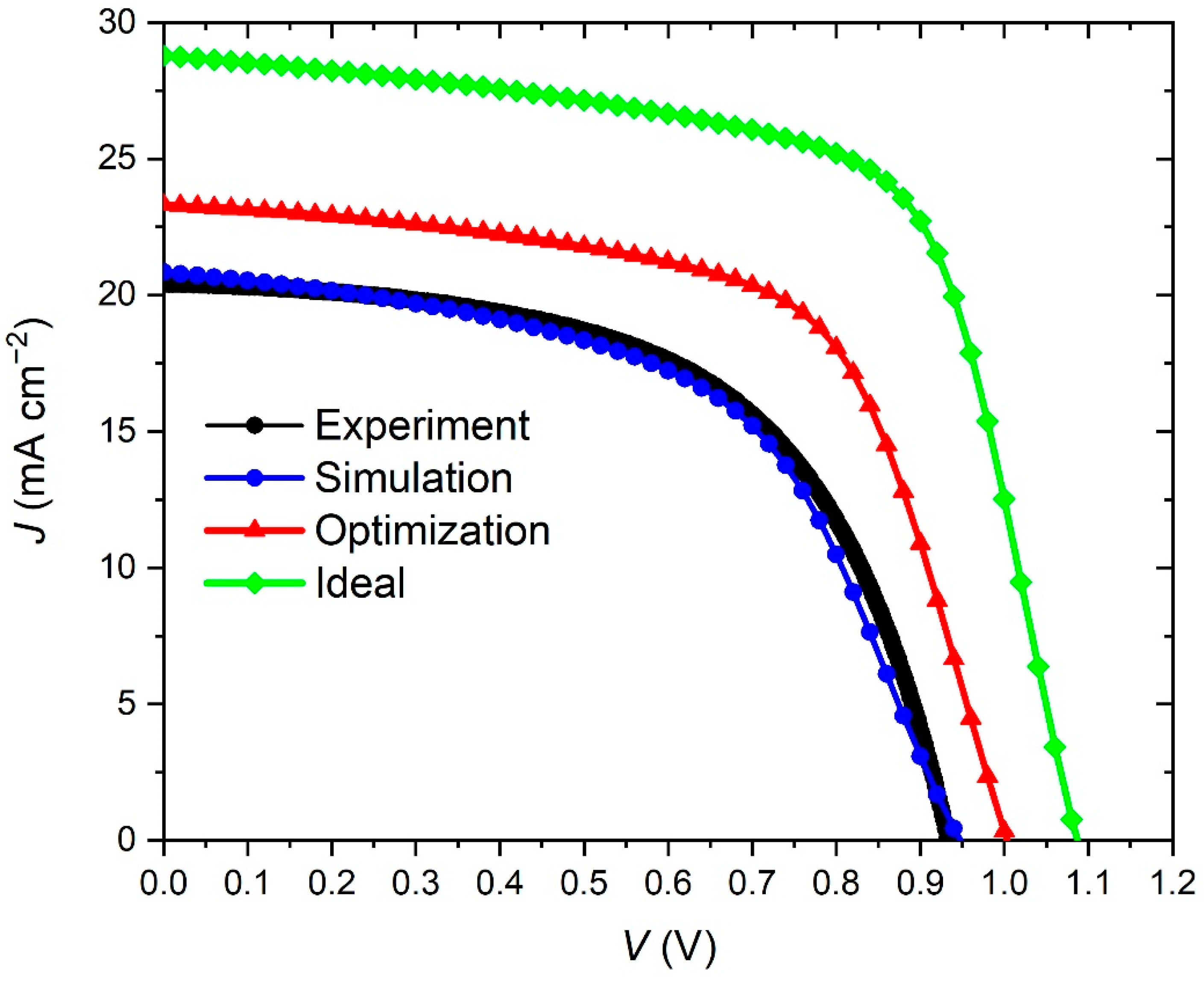
| Parameter | Experimental | Simulated |
|---|---|---|
| Voc (V) | 0.93 | 0.94 |
| Jsc (mA/cm2) | 20.44 | 20.80 |
| FF (%) | 57.62 | 54.29 |
| PCE (%) | 11.00 | 10.72 |
Publisher’s Note: MDPI stays neutral with regard to jurisdictional claims in published maps and institutional affiliations. |
© 2022 by the authors. Licensee MDPI, Basel, Switzerland. This article is an open access article distributed under the terms and conditions of the Creative Commons Attribution (CC BY) license (https://creativecommons.org/licenses/by/4.0/).
Share and Cite
Stanić, D.; Kojić, V.; Bohač, M.; Čižmar, T.; Juraić, K.; Rath, T.; Gajović, A. Simulation and Optimization of FAPbI3 Perovskite Solar Cells with a BaTiO3 Layer for Efficiency Enhancement. Materials 2022, 15, 7310. https://0-doi-org.brum.beds.ac.uk/10.3390/ma15207310
Stanić D, Kojić V, Bohač M, Čižmar T, Juraić K, Rath T, Gajović A. Simulation and Optimization of FAPbI3 Perovskite Solar Cells with a BaTiO3 Layer for Efficiency Enhancement. Materials. 2022; 15(20):7310. https://0-doi-org.brum.beds.ac.uk/10.3390/ma15207310
Chicago/Turabian StyleStanić, Denis, Vedran Kojić, Mario Bohač, Tihana Čižmar, Krunoslav Juraić, Thomas Rath, and Andreja Gajović. 2022. "Simulation and Optimization of FAPbI3 Perovskite Solar Cells with a BaTiO3 Layer for Efficiency Enhancement" Materials 15, no. 20: 7310. https://0-doi-org.brum.beds.ac.uk/10.3390/ma15207310