Article

Effect of Annealing Temperature and Oxygen Flow in the Properties of Ion Beam Sputtered SnO2x Thin Films

1
Department of Materials Science and Engineering, National Cheng Kung University, No. 1, University Road, Tainan 701, Taiwan
2
Department of Electrical Engineering, Cheng Shiu University, No. 840, Chengcing Road, Niaosong Township, Kaohsiung 833, Taiwan
3
Amity Institute of Nanotechnology, Amity University, Sector 125, Noida, India
4
Department of Chemical and Materials Engineering, National University of Kaohsiung, No. 700, Kaohsiung University Road, Nan-Tzu District, Kaohsiung 811, Taiwan
5
Center for Micro/Nano Science and Technology, National Cheng Kung University, Tainan 701, Taiwan
6
Research Center for Energy Technology and Strategy, National Cheng Kung University, Tainan 701, Taiwan
*
Author to whom correspondence should be addressed.
These authors contributed equally to this work.
Materials 2015, 8(8), 5289-5297; https://0-doi-org.brum.beds.ac.uk/10.3390/ma8085243
Submission received: 30 June 2015 / Revised: 5 August 2015 / Accepted: 6 August 2015 / Published: 14 August 2015
(This article belongs to the Special Issue Selected Papers from ICASI 2015)

Abstract

:
Tin oxide (SnO2−x) thin films were prepared under various flow ratios of O2/(O2 + Ar) on unheated glass substrate using the ion beam sputtering (IBS) deposition technique. This work studied the effects of the flow ratio of O2/(O2 + Ar), chamber pressures and post-annealing treatment on the physical properties of SnO2 thin films. It was found that annealing affects the crystal quality of the films as seen from both X-ray diffraction (XRD) and transmission electron microscopy (TEM) analysis. In addition, the surface RMS roughness was measured with atomic force microscopy (AFM). Auger electron spectroscopy (AES) analysis was used to obtain the changes of elemental distribution between tin and oxygen atomic concentration. The electrical property is discussed with attention to the structure factor.

1. Introduction

The most widely-used materials for transparent conductive oxide (TCO) thin films are zinc oxide (ZnO), tin oxide (SnO2) and indium oxide (In2O3). SnO2 thin films have been developed and applied in different fields, such as solar cells, gas sensors and light-emitting diodes (LEDs) [1,2,3,4,5] because they have the advantages of their low electrical resistance and high optical transparency in the visible range of the electromagnetic spectrum. Furthermore, they are inexpensive and also stable against thermal and chemical attacks at high temperature.
A number of studies have been reported on the effect of the oxygen gas ratio [6], substrate temperature and type, annealing temperature [7,8,9] and doping elements [10,11,12] on improving the structural, electrical and optical properties of the SnO2 thin film in the past few decades. The thin films of pure or doped SnO2 can be prepared by different deposition techniques, including sol-gel-dip coatings [13], metal-organic chemical vapor deposition (MOCVD) [14,15], chemical bath deposition (CBD) [16], spray pyrolysis [17], electron beam evaporation [18] and sputtering [19,20,21,22]. However, it is necessary to carry out either a heat treatment of substrates during the deposition process or the post-annealing procedure to obtain low resistivity and to retain high transmittance. Here, the ion beam sputtering (IBS) technique was applied to achieve high quality films, because of its high energy of incoming ions and the low deposition rate.
In general, SnO2 thin films have defects, such as oxygen vacancies [23], which act as donors in the SnO2 matrix and increase the electron density in the conduction band. This is called the n-type conduction. The formation of excess oxygen vacancies results in decreasing film quality. Thus, increasing the conductivity of SnO2−x lies in a narrow range of oxygen pressure [24]. The post-heat treatment reduces residual stress and the lattice mismatch to obtain good electrical conductivity [25].
In the present work, we investigated the effects of the flow ratio of O2/(O2 + Ar), chamber pressures and post-annealing treatment on the physical properties of SnO2 thin films.

2. Results and Discussion

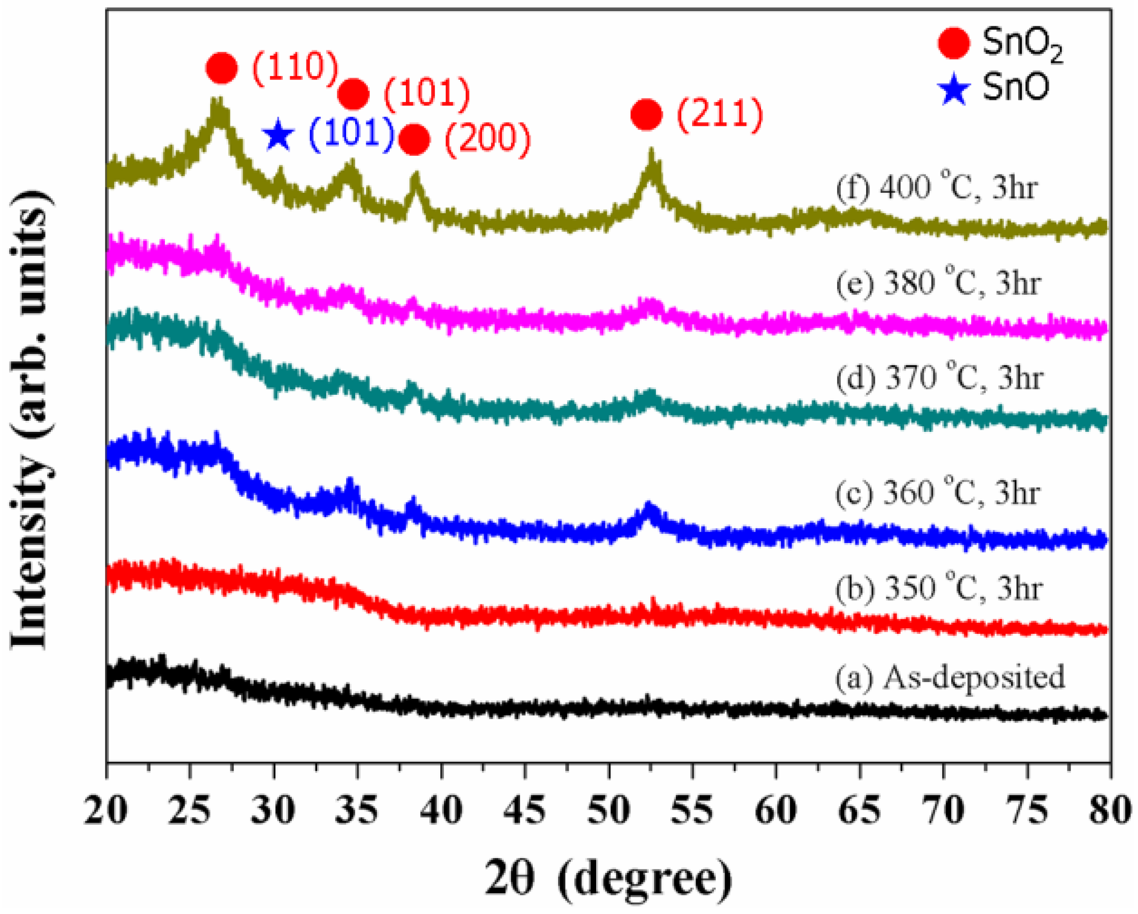
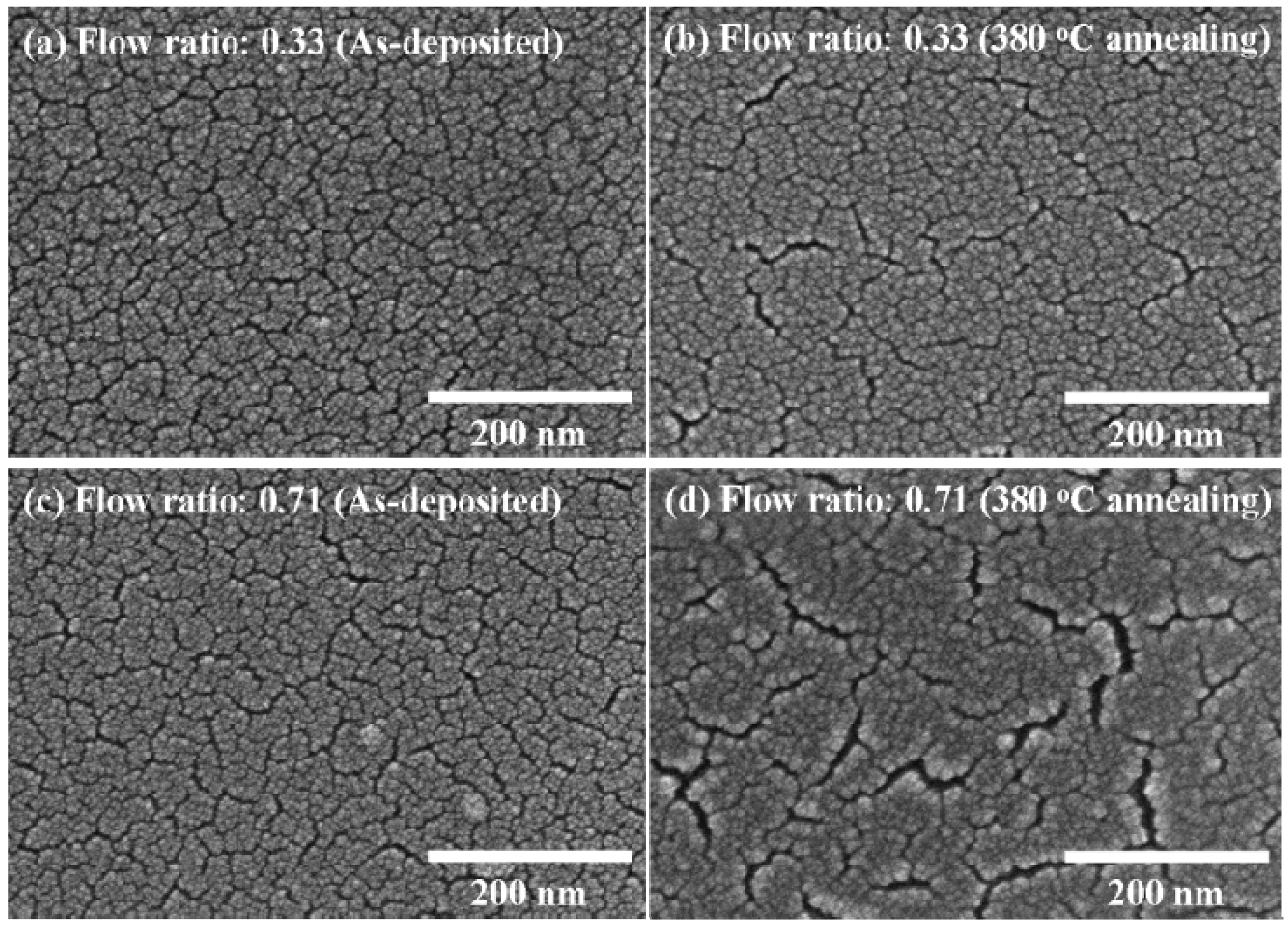
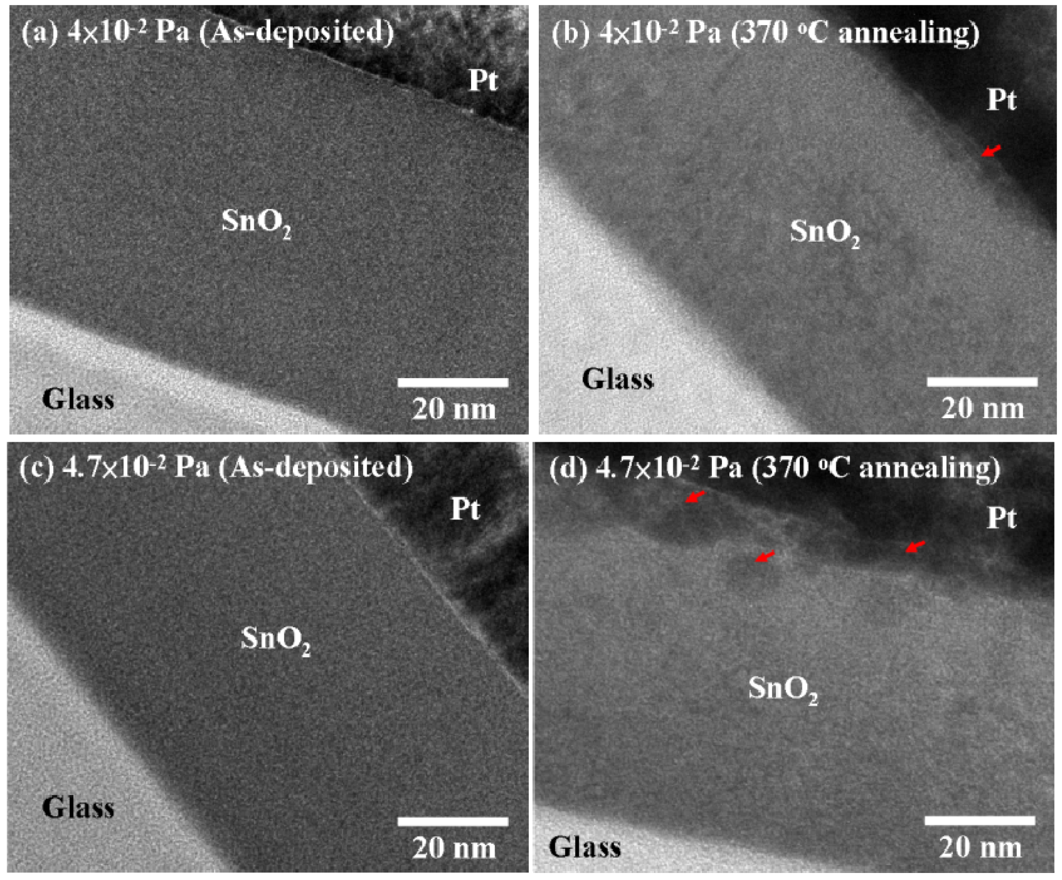
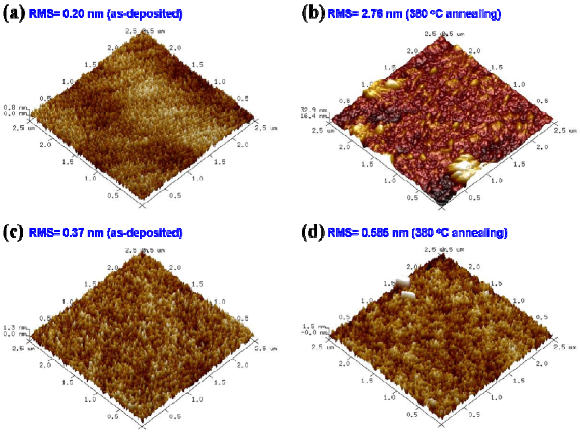
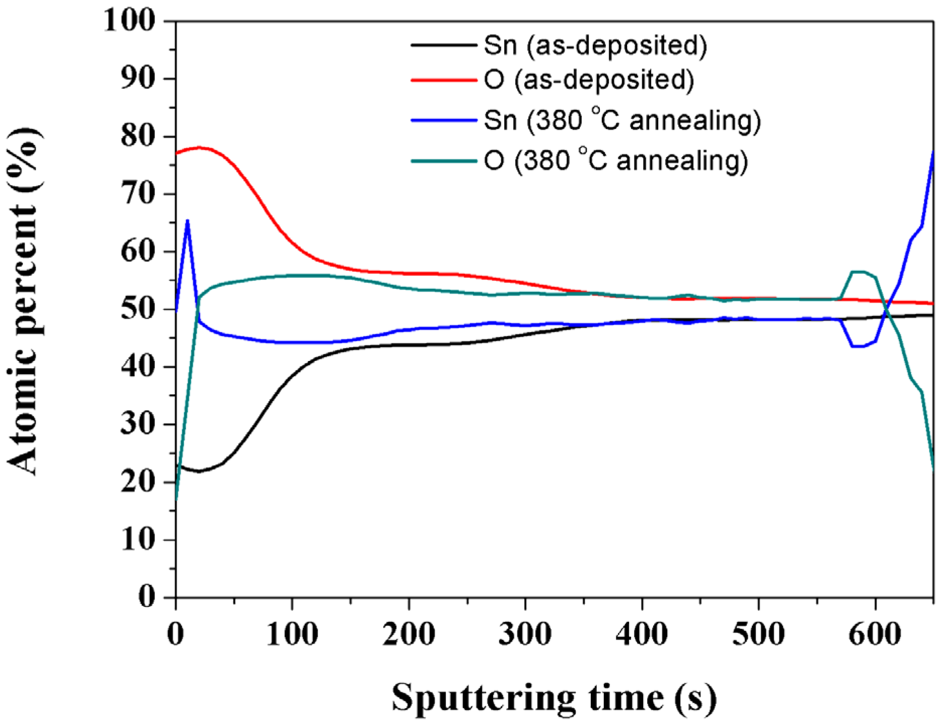
2.1. Structural and Morphological Properties

Figure 1 shows typical XRD patterns of the as-deposited and annealed SnO2−x films where they were prepared at a flow ratio of 0.5 of O2/(O2 + Ar) at 4.7 × 10⁻² Pa. The structures of the as-deposited and the annealed SnO2−x films deposited at 4 × 10⁻² Pa were almost the same as that prepared. It is observed that the films as-deposited and annealed at 350 °C were the typical amorphous structure, as indicated in Figure 1a,b. However, SnO2−x films annealed at 360 °C have crystallization without preferred orientations, as shown in Figure 1c. A similar result was reported by Wulff et al. [26] for ITO thin films. Further, the {101} peak of SnO phase appeared at 400 °C, as shown in Figure 1f, which was also reported by Choe et al. [9].
Figure 1. XRD patterns of SnO2−x thin films (a) as-deposited and annealed for 3 h at (b) 350 °C; (c) 360 °C; (d) 370 °C; (e) 380 °C and (f) 400 °C at 4.7 × 10⁻² Pa.
Materials 08 05243 g001
Figure 2 shows the surface morphology of SnO2−x films prepared with low and high flow ratios of 0.33 and 0.71 at 4 × 10⁻² Pa. It is observed that the as-deposited films have similar and uniform surface morphologies. However, cracks are found at a high O2/(O2 + Ar) flow ratio of 0.71 after 380 °C annealing.
Figure 2. FE-SEM micrographs of the SnO2−x thin films prepared at various flow ratios and a working pressure of 4 × 10⁻² Pa. The flow ratio of 0.33 of O2/(O2 + Ar) (a) for as-deposited films; (b) 380 °C annealing and the flow ratio of 0.71 of O2/(O2 + Ar) (c) for as-deposited films; (d) 380 °C annealing.
Materials 08 05243 g002
In addition to SEM analysis, TEM was employed to characterize the cross-section of SnO2−x films. The as-deposited films with a high flow ratio of 0.71 of O2/(O2 + Ar) at 4 × 10⁻² and 4.7 × 10⁻² Pa reveal very high adherence and a smooth and uniform surface, as shown in Figure 3a,c. After annealing at 370 °C for 3 h, the films show looser, thinner interfaces than as-deposited films, because they were cracked and have enhanced large spaces between grains after high temperature Ar annealing, as shown in Figure 3b,d.
Figure 3. The cross-section images of bright field high-resolution TEM analysis at the same flow ratio of 0.71 of O2/(O2 + Ar) and a working pressure of 4 × 10⁻² Pa (a) for as-deposited films; (b) 370 °C annealing and a working pressure of 4.7 × 10⁻² Pa (c) for as-deposited films; (d) 370 °C annealing.
Materials 08 05243 g003
Figure 4. 3D AFM images with a scan area of 2.5 μm × 2.5 μm: (a) as-deposited; (b) 380 °C annealing SnO2−x thin films at the flow ratio of 0.5 of O2/(O2 + Ar) and a working pressure of 4 × 10⁻² Pa. (c) As-deposited; (d) 380 °C annealing SnO2−x thin films at the flow ratio of 0.5 of O2/(O2 + Ar) and a working pressure of 4.7 × 10⁻² Pa.
Materials 08 05243 g004
The AFM images that illustrate the surface topology and the root mean square (RMS) surface roughness of SnO2−x films before and after 380 °C annealing are shown in Figure 4. It is clear that the surface morphology of the as-deposited film and 380 °C annealing at the flow ratio of 0.5 of O2/(O2 + Ar) do not significantly change at a working pressure of 4.7 × 10⁻² Pa, as shown in Figure 4c,d. However, the surface morphology of the film changes dramatically from Figure 4a to Figure 4b. The surface roughness of the as-deposited film at 4 × 10² Pa is 0.20 nm. The film annealed at 380 °C shows an increase of surface roughness from 0.20 nm to 2.76 nm. The increase in film roughness at a working pressure of 4 × 10⁻² Pa can be explained with surface melt after 380 °C annealing. However, it does not have an obvious structure transformation at a working pressure of 4.7 × 10⁻² Pa.

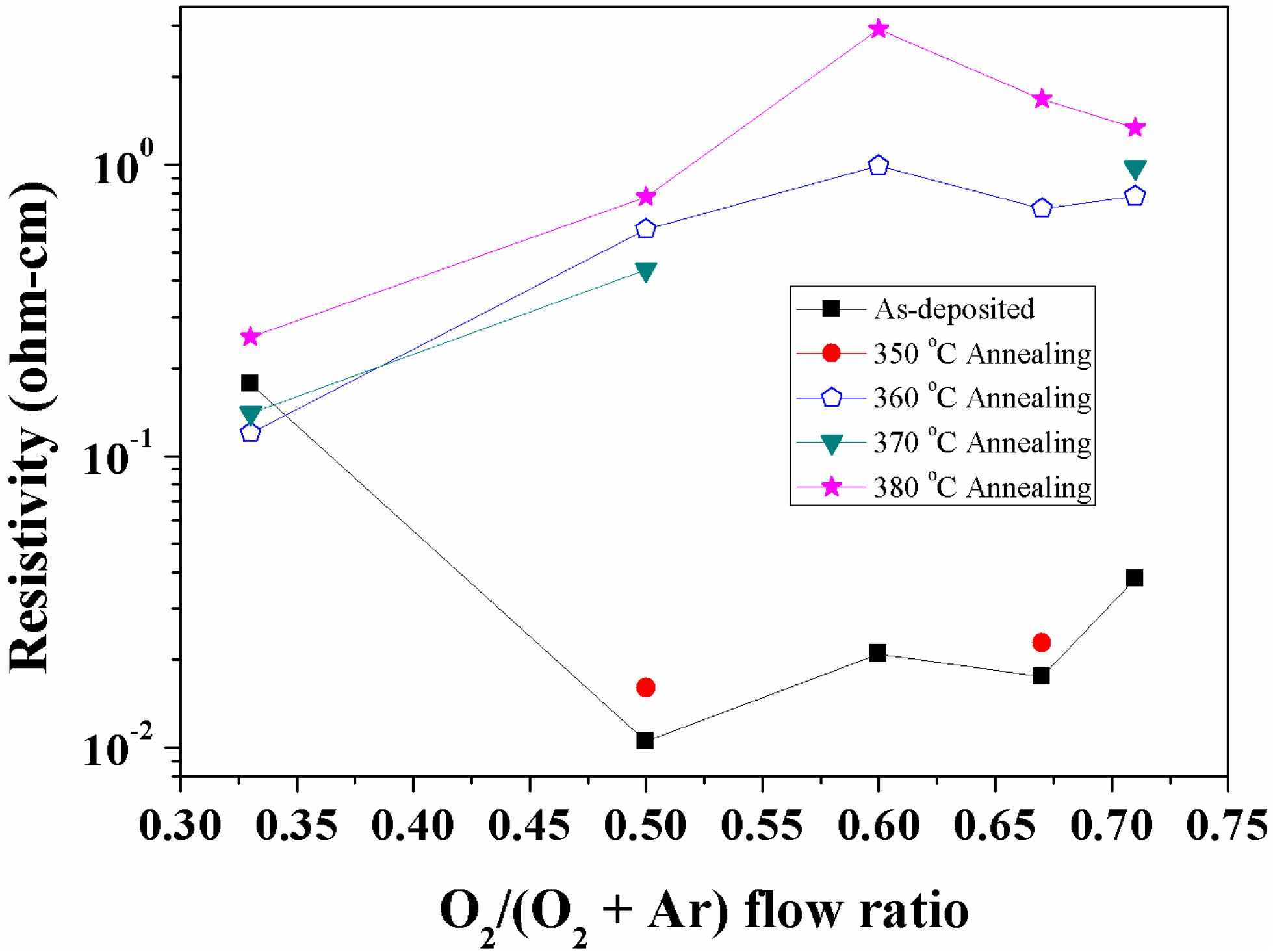
2.2. Electrical Properties

Figure 5 shows the variation of electrical resistivity of SnO2 thin films with various flow ratios of O2/(O2 + Ar) at the annealing temperature from 350 °C to 380 °C and a working pressure of 4.7 × 10⁻² Pa.
Figure 5. The variation of the electrical resistivity of SnO2−x thin films with various flow ratios of O2/(O2 + Ar) at the annealing temperature from 350 °C to 380 °C and a working pressure of 4.7 × 10⁻² Pa.
Materials 08 05243 g005
The as-deposited films show the lowest resistivity of 1.05 × 10⁻² Ω cm at the flow ratio of 0.5. A strong dependence of resistivity on the oxygen flow ratio was observed. It is observed that the resistivity increased about two orders of higher magnitude at 360 °C than that of the as-deposited films, except at the flow ratio of 0.33. This is due to the change in the structure from amorphous to crystallization and mainly the decrease of carrier concentration with a serious crack formation at a higher flow ratio, as depicted by SEM and TEM analyses. Shanthi et al. [27] reported that the chemisorbed oxygen removes oxygen vacancies at high temperature annealing and increases chemisorbed oxygen at the surfaces and grain boundaries, which results from further lowering of free electrons. The degree of reduction in carrier concentration was high for SnO2 deposited at a high flow ratio. At the oxygen flow ratio of 0.3, the initial decrease in resistivity at the annealing temperature from 360 °C to 370 °C is due to the number of oxygen vacancies and excess metal ions arising from the non-stoichiometry, which was also reported by Ku et al. [28]. The flow ratio of 0.6 has the highest resistivity due to its lowest mobility or carrier concentration at high and low working pressure after annealing. Williams and Ho [29,30] reported the conductivity performance of SnO2 sensors, which were very a sensitive probe of changes in surface chemistry due to electrons transfer, such as the parameters of oxygen partial pressure and crystallite size, etc.
Figure 6 shows the AES depth profile of as-deposited and 380 °C annealing SnO2−x thin films at the flow ratio of 0.5 of O2/(O2 + Ar) and a working pressure of 4.7 × 10⁻² Pa. The depth profile shows the change of atomic percent at the sputtering time from 0 to 120 s. The change of composition after the annealing temperature of 380 °C indicates the decrease of oxygen atoms and the increase of tin atoms in the thin film surface. The AES profiles are usually used for chemical composition analysis. We used this technique to confirm the correction for the thickness and atomic percentage with TEM.
Figure 6. Atomic depth profile of the as-deposited and 380 °C annealing SnO2−x thin films at the flow ratio of 0.5 of O2/(O2 + Ar) and a working pressure of 4.7 × 10⁻² Pa.
Materials 08 05243 g006

3. Experimental Section

Thin films of SnO2 were sputtered from a diameter of 4-inch using a high purity of 99.99 wt% SnO2 ceramic target (Ultimate Materials Technology Co., Hsinchu, Taiwan) in an atmosphere of argon and oxygen gases having 99.999% purity. SnO2 layers of about 60 nm in thickness were deposited onto the glass substrates (Corning EAGLE 2000 AMLCD glass, Taichung, Taiwan) using an ion beam sputtering deposition system, the Commonwealth Scientific IBS250 Kaufman ion source, at the conditions of 600 V and 20 A, where the glass substrates were heated at 373 K. The vacuum of the ion beam sputtering chamber was maintained at 3 × 10⁻⁴ Pa before deposition. In the case of ion beam sputtering of SnO2 films, the flow ratio of mixture gas composition O2/(O2 + Ar) was controlled from 0.33 to 0.71 at a working pressure of 4.7 × 10⁻² and 4.0 × 10⁻² Pa during deposition. The as-deposited SnO2 films were subsequently annealed in Ar atmosphere from 350 °C to 400 °C for 3 h. The phase and lattice structure of the films were analyzed using grazing angle X-ray diffraction (XRD) (D/Max2500 Rigaku, Tokyo, Japan) with Cu Kα radiation (λ = 1.5406 Å) at 40 kV and 100 mA. The field-emission scanning electron microscope (FE-SEM) (S4800-I Hitachi, Tokyo, Japan) was used to observe the surface topography of the films before and after annealing at 15 kV. The cross-section morphologies of as-deposited and post-annealing films were investigated by an ultrahigh resolution transmission electron microscopy (HR-TEM) (JEM-2100F, JEOL, Peabody, MA, USA) at 200 kV, which was equipped with an energy dispersive spectrometer (EDS) INCA x-stream-2 Oxford, U.K., for chemical elemental analysis. For EDS measurements, a silicon drift detector of 80 mm2 was used. TEM samples were prepared using focus ion beams SMI3050SE (SEIKO, Chiba, Japan) with the first milling at 30 kV and 100 pA and the final milling at 5 kV and 40 pA. After that, Pt was coated on the SnO2 surface to protect thin films from damage. The Hall effect measurement setup AHM-800A with Advance Design Technology in van der Pauw configuration was used to study the electrical properties. Atomic force microscopy (AFM) (Force Precision Instrument Co., Taipei, Taiwan) was used to evaluate the surface roughness of the films by tapping mode. The sample surface was probed with a silicon tip of 10 nm in radius oscillating at its resonant frequency between 200 and 400 kHz. The scan area was 2.5 μm × 2.5 μm, and the scan rate was 0.3 Hz. The compositions and depth profile of the films were determined by the Auger Electron Spectroscopy (AES) (Microlab 350, Thermo Fisher Scientific, Warrangton, UK).

4. Conclusions

As-deposited SnO2 thin films show an amorphous structure, and crystallization occurs at 360 °C. The resistivity of the film depends strongly on the oxygen flow ratio of 0.5 and above, due to the decrease in carrier concentration. In the case of an oxygen flow ratio of 0.3, metallic ions are dominated, and stable conductivity after annealing is observed due to the change in the numbers of oxygen vacancies and excess metal ions. Therefore, the dependence of resistivity on the oxygen partial pressure could be interesting in view of the use of these materials as oxygen sensors.

Acknowledgments

The authors acknowledge Sean Wu for the assistance in the measurement apparatus of the Hall effect at the College of Applied Design, TungFang Design Institute. The authors wish to thank H.C. Liu of the Department of Materials Science and Engineering, National Cheng Kung University, for giving great help with the AFM instrument in this work. This project was financially supported by the National Science Council of Taiwan with Grant No. 101-2221-E-006-124-MY3.

Author Contributions

All authors made contributions to this manuscript. Chun-Min Wang performed the experimental works, analyzed the results and wrote the manuscript. Chun-Chieh Huang and Dipti Ranjan Sahu greatly contributed to the concept and the design of the experimental parameters. Jui-Chao Kuo strongly contributed to the discussion of all of the results and revised the manuscript. Jow-Lay Huang provided overall guidance.

Conflicts of Interest

The authors declare no conflict of interest.

References

  1. Snaith, H.J.; Ducati, C. SnO2-based dye-sensitized hybrid solar cells exhibiting near unity absorbed photon-to-electron conversion efficiency. Nano Lett. 2010, 10, 1259–1265. [Google Scholar] [CrossRef] [PubMed]
  2. Nang Dinh, N.; Bernard, M.-C.; Hugot-Le Goff, A.; Stergiopoulos, T.; Falaras, P. Photoelectrochemical solar cells based on SnO2 nanocrystalline films. Comptes Rendus Chim. 2006, 9, 676–683. [Google Scholar] [CrossRef]
  3. Tricoli, A.; Graf, M.; Pratsinis, S.E. Optimal doping for enhanced SnO2 sensitivity and thermal stability. Adv. Funct. Mater. 2008, 18, 1969–1976. [Google Scholar] [CrossRef]
  4. Song, J.-O.; Seong, T.-Y. Highly transparent Ag/SnO2 ohmic contact to p-type GaN for ultraviolet light-emitting diodes. Appl. Phys. Lett. 2004, 85, 6374–6376. [Google Scholar] [CrossRef]
  5. Jeng, C.-C.; Chong, P.J.H.; Chiu, C.-C.; Jiang, G.-J.; Lin, H.-J.; Wu, R.-J.; Wu, C.-H. A dynamic equilibrium method for the SnO2-based ozone sensors using UV-LED continuous irradiation. Sens. Actuators B Chem. 2014, 195, 702–706. [Google Scholar] [CrossRef]
  6. Lee, J. Effects of oxygen concentration on the properties of sputtered SnO2:Sb films deposited at low temperature. Thin Solid Films 2008, 516, 1386–1390. [Google Scholar] [CrossRef]
  7. Khan, A.F.; Mehmood, M.; Rana, A.M.; Bhatti, M.T. Effect of annealing on electrical resistivity of RF-magnetron sputtered nanostructured SnO2 thin films. Appl. Surf. Sci. 2009, 255, 8562–8565. [Google Scholar] [CrossRef]
  8. Rembeza, E.S.; Richard, O.; Landuyt, J.V. Influence of laser and isothermal treatments on microstructural properties of SnO2 films. Mater. Res. Bull. 1999, 34, 1527–1533. [Google Scholar] [CrossRef]
  9. Choe, Y.-S.; Chung, J.-H.; Kim, D.-S.; Kim, G.-H.; Baik, H.K. Phase transformation and morphological evolution of ion-beam sputtered tin oxide films on silicon substrate. Mater. Res. Bull. 1999, 34, 1473–1479. [Google Scholar] [CrossRef]
  10. Zhu, Q.; Ma, Q.; Buchholz, D.B.; Chang, R.P.H.; Bedzyk, M.J.; Mason, T.O. Structural and physical properties of transparent conducting, amorphous Zn-doped SnO2 films. J. Appl. Phys. 2014, 115, 033512. [Google Scholar] [CrossRef]
  11. Mohanapriya, P.; Pradeepkumar, R.; Victor Jaya, N.; Natarajan, T.S. Magnetic and optical properties of electrospun hollow nanofibers of SnO2 doped with Ce-ion. Appl. Phys. Lett. 2014, 105, 022406. [Google Scholar] [CrossRef]
  12. Stjerna, B.; Olsson, E.; Granqvist, C.G. Optical and electrical properties of radio frequency sputtered tin oxide films doped with oxygen vacancies, F, Sb, or Mo. J. Appl. Phys. 1994, 76, 3797–3817. [Google Scholar] [CrossRef]
  13. Floriano, E.A.; Scalvi, L.V.D.A.; Sambrano, J.R.; Geraldo, V. Evaluation of bulk and surfaces absorption edge energy of sol-gel-dip-coating SnO2 thin films. Mater. Res. 2010, 13, 437–443. [Google Scholar] [CrossRef]
  14. Duverneuil, P.; Maury, F.; Pebere, N.; Senocq, F.; Vergnes, H. Chemical vapor deposition of SnO2 coatings on Ti plates for the preparation of electrocatalytic anodes. Surf. Coat. Technol. 2002, 151–152, 9–13. [Google Scholar] [CrossRef]
  15. Feng, X.; Ma, J.; Yang, F.; Ji, F.; Zong, F.; Luan, C.; Ma, H. Transparent conducting SnO2:Sb epitaxial films prepared on α-Al2O3 (0001) by MOCVD. Mater. Lett. 2008, 62, 1779–1781. [Google Scholar] [CrossRef]
  16. Ebrahimiasl, S.; Yunus, W.M.Z.W.; Kassim, A.; Zainal, Z. Synthesis of nanocrystalline SnOx (x = 1–2) thin film using a chemical bath deposition method with improved deposition time, temperature and pH. Sensors 2011, 11, 9207–9216. [Google Scholar] [CrossRef] [PubMed]
  17. Agashe, C.; Mahamuni, S. Competitive effects of film thickness and growth rate in spray pyrolytically deposited fluorine-doped tin dioxide films. Thin Solid Films 2010, 518, 4868–4873. [Google Scholar] [CrossRef]
  18. Punitha, K.; Sivakumar, R.; Sanjeeviraja, C. Structural and surface morphological studies of magnesium tin oxide thin films. Energy Procedia 2012, 15, 312–317. [Google Scholar] [CrossRef]
  19. Jäger, S.; Szyszka, B.; Szczyrbowski, J.; Bräuer, G. Comparison of transparent conductive oxide thin films prepared by a.c. and d.c. reactive magnetron sputtering. Surf. Coat. Technol. 1998, 98, 1304–1314. [Google Scholar] [CrossRef]
  20. Ding, X.; Fang, F.; Jiang, J. Electrical and optical properties of N-doped SnO2 thin films prepared by magnetron sputtering. Surf. Coat. Technol. 2013, 231, 67–70. [Google Scholar] [CrossRef]
  21. Becker, M.; Hamann, R.; Polity, A.; Meyer, B.K. Stannic oxide thin film growth via ion-beam-sputtering. Thin Solid Films 2014, 553, 26–29. [Google Scholar] [CrossRef]
  22. Tosun, B.S.; Feist, R.K.; Gunawan, A.; Mkhoyan, K.A.; Campbell, S.A.; Aydil, E.S. Sputter deposition of semicrystalline tin dioxide films. Thin Solid Films 2012, 520, 2554–2561. [Google Scholar] [CrossRef]
  23. Jarzebski, Z.M.; Marton, J.P. Physical properties of SnO2 materials: II. Electrical properties. J. Electrochem. Soc. 1976, 123, 299C–310C. [Google Scholar] [CrossRef]
  24. Wang, C.-M.; Huang, C.-C.; Kuo, J.-C.; Lin, H.-T.; Huang, J.-L. Preparing transparent conductive Sn/SbO2−x thin films by annealing bi-layer Sb/SnO2 with pulse UV laser. Mater. Lett. 2012, 72, 29–31. [Google Scholar] [CrossRef]
  25. Ordaz-Flores, A.; Bartolo-Pérez, P.; Castro-Rodríguez, R.; Oliva, A. Annealing effects on the mass diffusion of the CdS/ITO interface deposited by chemical bath deposition. Rev. Mex. Fís. 2006, 52, 15–18. [Google Scholar]
  26. Wulff, H.; Quaas, M.; Steffen, H.; Hippler, R. In situ studies of diffusion and crystal growth in plasma deposited thin ITO films. Thin Solid Films 2000, 377–378, 418–424. [Google Scholar] [CrossRef]
  27. Shanthi, E.; Banerjee, A.; Dutta, V.; Chopra, K.L. Annealing characteristics of tin oxide films prepared by spray pyrolysis. Thin Solid Films 1980, 71, 237–244. [Google Scholar] [CrossRef]
  28. Ku, D.Y.; Kim, I.H.; Lee, I.; Lee, K.S.; Lee, T.S.; Jeong, J.H.; Cheong, B.; Baik, Y.J.; Kim, W.M. Structural and electrical properties of sputtered indium–zinc oxide thin films. Thin Solid Films 2006, 515, 1364–1369. [Google Scholar] [CrossRef]
  29. Williams, D.E. Oxide Gas Sensors. In Encyclopedia of Materials: Science and Technology, 2nd ed.; Elsevier: Oxford, UK, 2001; pp. 6609–6613. [Google Scholar]
  30. Ho, G.W. Gas Sensor with Nanostructured Oxide Semiconductor Materials. Sci. Adv. Mater. 2011, 3, 150–168. [Google Scholar] [CrossRef]

