Article

Metal Nanoparticle-Decorated Two-Dimensional Molybdenum Sulfide for Plasmonic-Enhanced Polymer Photovoltaic Devices

Department of Photonics, National Chiao Tung University, Hsinchu 30010, Taiwan
*
Author to whom correspondence should be addressed.
Materials 2015, 8(8), 5414-5425; https://0-doi-org.brum.beds.ac.uk/10.3390/ma8085252
Submission received: 25 June 2015 / Revised: 6 August 2015 / Accepted: 18 August 2015 / Published: 21 August 2015
(This article belongs to the Special Issue Plasmonic Materials)

Abstract

:
Atomically thin two-dimensional (2D) transition metal dichalcogenides have also attracted immense interest because they exhibit appealing electronic, optical and mechanical properties. In this work, we prepared gold nanoparticle-decorated molybdenum sulfide (AuNP@MoS2) through a simple spontaneous redox reaction. Transmission electron microscopy, UV-Vis spectroscopy, and Raman spectroscopy were used to characterize the properties of the AuNP@MoS2 nanomaterials. Then we employed such nanocomposites as the cathode buffer layers of organic photovoltaic devices (OPVs) to trigger surface plasmonic resonance, leading to noticeable enhancements in overall device efficiencies. We attribute the primary origin of the improvement in device performance to local field enhancement induced by the effects of localized surface plasmonic resonance. Our results suggest that the metal nanoparticle-decorated two-dimensional materials appear to have great potential for use in high-performance OPVs.

1. Introduction

Organic photovoltaic devices (OPVs) have received a great deal of attention because they feature many advantageous properties, including light weight, low cost, mechanical flexibility and short energy payback time [1,2,3]. To date, the power conversion efficiencies (PCEs) of the single-junction devices have broken through 10% [4]. Moreover, the internal quantum efficiency (IQE) of state-of-art OPVs can approach 100%, meaning that nearly every absorbed photon can be converted to charge carriers and that all the carriers are collected at the electrodes [5]. Because the overall quantum efficiency is governed by the IQE and absorption efficiency, efficient light absorption in OPVs is still critical for further improving the PCEs. One approach for increasing the absorption efficiency is to develop light trapping techniques [6,7,8,9,10,11,12]. For example, using optical spacers [7,8] and photonic crystals [9] have been recently proposed. Among the light-trapping schemes, incorporation of metal nanostructures, which can trigger surface plasmons (SPs), have been proved to be a promising way for increasing the light harvesting ability of OPVs [10,11,12,13,14,15,16,17,18,19,20,21,22,23]. As metal nanoparticles (NPs) can be readily synthesized and incorporated into the devices via simple solution processes, they have become the most widely used plasmonic nanostructures for enhancing the PCEs of OPVs [11,12,13].
Atomically thin two-dimensional (2D) transition metal dichalcogenides (TMDs) have also attracted immense interest because they exhibit appealing electronic, optical and mechanical properties [24,25,26,27,28,29]. In particular, the TMDs that having direct band gaps, such as MoS2 and WS2, have been employed in many applications [24,25], including field effect transistors [26], photodetectors [27], light-emitting devices [28] and sensors [29]. Further, these TMDs have been incorporated into OPVs as interfacial buffer layers for improving their device stability and/or efficiencies [30,31,32,33,34]. More interestingly, the work-function of the TMD interfacial layers can be modulated by p- or n-doping treatments [30]. Therefore, 2D TMDs can be considered as promising building blocks for preparing materials exhibiting various functionalities. Recently, Yang et al. prepared a hole transport layer composed of ultrathin 2D MoS2 nanosheets decorated with Au NPs for triggering the plasmonic effects in OPVs [35]. From both simulation and experimental results, they have shown that the nanocomposites can utilize the plasmonic near-field more efficiently, particularly along the horizontal direction, thereby leading to apparent efficiency improvement.
In this work, we have prepared MoS2 nanosheets using a very simple, greener liquid phase exfoliation method [36]. A surfactant was added into the suspension of bulk MoS2, and, thereby, a stable aqueous dispersion of exfoliated MoS2 sheets could be obtained after sonication. The resulting nanosheets were further decorated with Au NPs through a spontaneous redox reaction with hexachloroauric acid, resulting in a novel nanostructure of Au NP-decorated MoS2 (AuNP@MoS2) nanocomposites [37]. Note that no additional reducing agent was required to reduce the Au ions. The as–synthesized AuNP@MoS2 could be readily incorporated into the OPVs as an interfacial buffer layer between the active layer and the electrodes. We have found that the Au NPs anchored on the MoS2 nanosheets induced the SR effects, which could effectively improve the device performance.

2. Results and Discussion

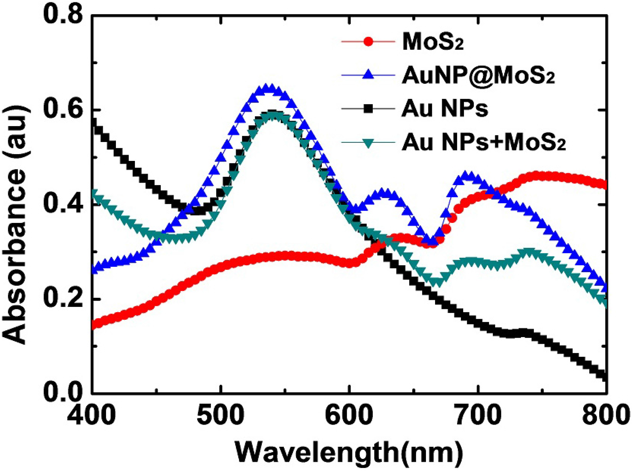
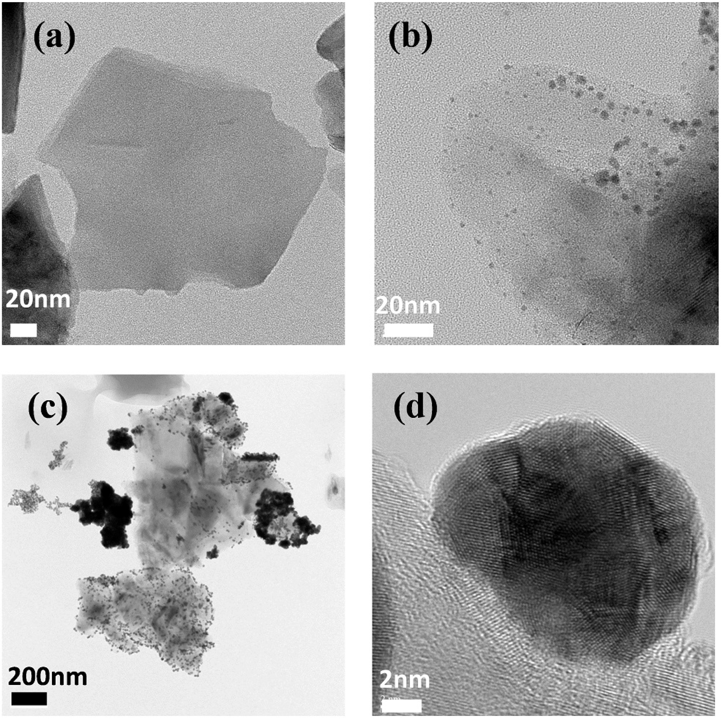
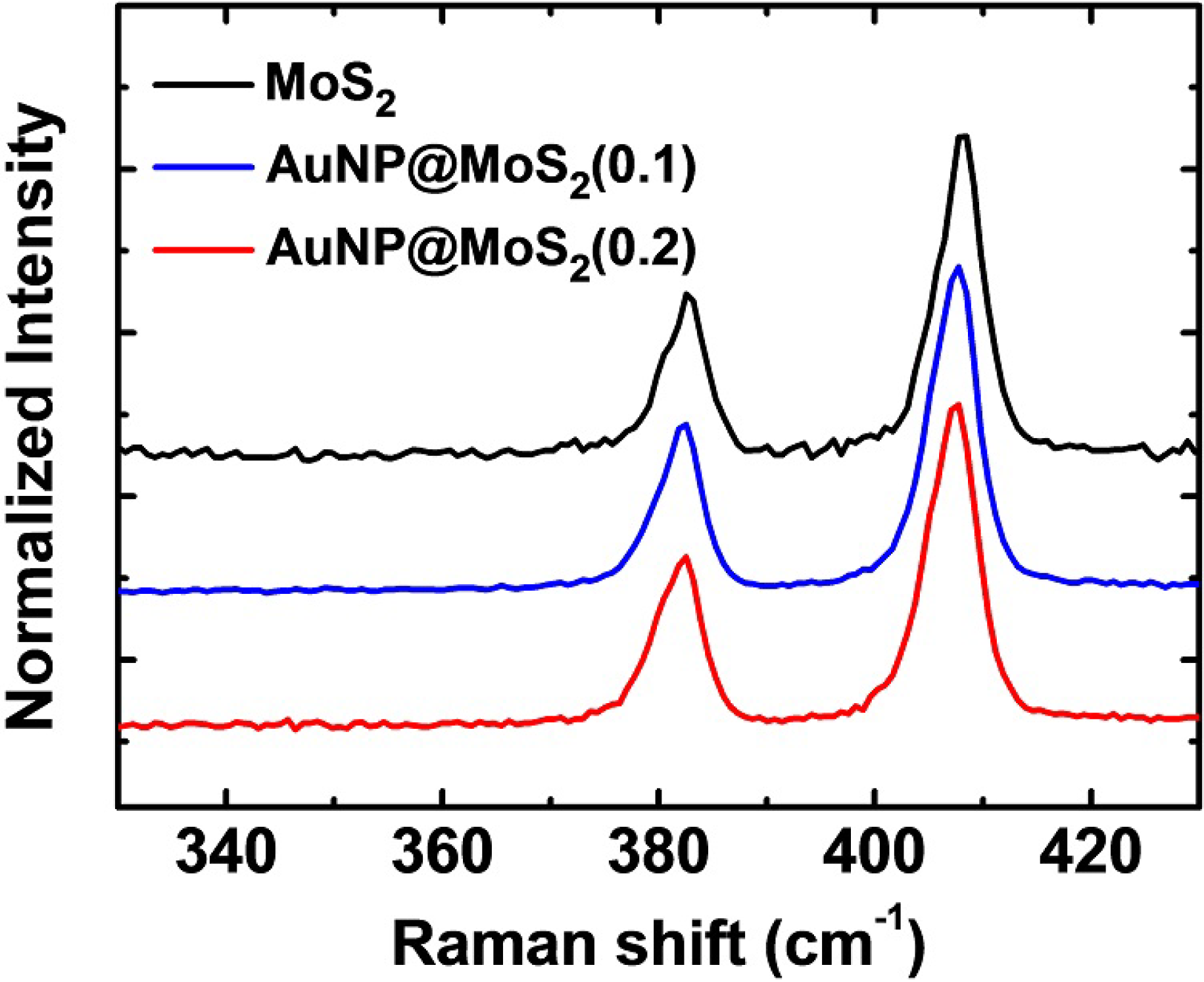
2.1. Synthesis and Characteristics of Au NP-Decorated MoS2 Nanocomposites

To prepare the AuNP@MoS2 nanocomposites, bulk MoS2 was exfoliated through a liquid phase method [36]. A triblock copolymer, poly(ethylene glycol)-block-poly(propylene glycol)-block- poly(ethylene glycol) (Pluronic P123) was added into an aqueous suspension of bulk MoS2. It behaved as a surfactant to reduce and maintain the surface tension of the aqueous phase for efficient exfoliation [36]. As a result, a stable dispersion of MoS2 nanosheets could be obtained after sonication. Then, a solution of HAuCl4 that was dissolved in de-ionized (DI) water was mixed with the resulting MoS2 solution. We found that Au ions were spontaneously reduced and anchored on the surface of exfoliated nanosheets. No additional reducing agent was required in this spontaneous reaction [37].
Figure 1 displays the absorption spectra of the MoS2 nanosheets suspended in water; several features of the spectrum are similar to those reported previously [38]. First, two excitonic peaks at 690 and 645 nm, which are termed A and B excitons, respectively, could be observed. They are related to the interband excitonic transitions at the K point of the Brillouin zone for the nanosheets with large lateral dimensions. The energy difference between the two excitonic peaks is due to the effect of spin–orbital coupling of the valence band [36,39]. Second, we also clearly observed one more peak at 745 nm, which was primarily due to scattering [38]. Such scattering effects could be resulted from the highly anisotropic structure, poor dispersion of the nanosheets, and damaged surfaces [39]. Note that the much larger scattering cross section of the scattering peak significantly distorted the intensities and locations of the previous excitonic peaks [38]. Further, we also observed a broad absorption band centered ca. 540 nm. It has been previously assigned as the blue-shifted excitonic peak due to the quantum size effect, indicating that the presence of nanosheets with lateral dimensions less than 50 nm [38].
Figure 1. Absorption spectra of the nanocomposites dispersed in aqueous solutions, including Au NP-decorated MoS2 (AuNP@MoS2), Au nanoparticles (Au NPs), the MoS2 nanosheets (MoS2) and the mixture of the Au NPs and MoS2 nanosheets (Au NPs + MoS2).
Materials 08 05252 g001
Meanwhile, Figure 2a shows the transmission electron microscopy (TEM) image of the MoS2 nanosheets; the plane size was primarily around 100 nm. In addition, we can also see the coexistence of mono-layer to few-layer of MoS2. After MoS2 was exfoliated, we further anchored the Au NPs on the MoS2 nanosheets through a spontaneous reduction method [37]. An aqueous HAuCl4 solution was added to the as-prepared MoS2 suspension. Because the Fermi level of MoS2 is situated above the reduction potential of AuCl4, spontaneous electron transfer from MoS2 to Au ions occurred, resulting in the formation of Au NPs on the MoS2 surfaces. Figure 2b,c displays the TEM images of the AuNP@MoS2 nanocomposites prepared with different concentrations of Au ions. While the concentration of HAuCl4 was 0.1 mg·mL−1, we clearly found the Au NPs decorated on the MoS2 basal planes. The particle size mainly ranged from 2 to 12 nm and the average size was ca. 6 nm. The image also shows the preferential edge decoration of the Au NPs, suggesting the reaction preferentially occurred at the highly energetic defect sites [37]. After the concentration of Au ions was increased to 0.2 mg·mL−1, more Au NPs were present on the nanosheets. The size of the NPs was slightly increased and the NPs also started to aggregate (Figure 2c). Figure 2d displays the TEM images with a higher magnification. We can see that the Au NP was bonded closely on the MoS2 surface. This image suggests that the Au ions were reduced by the nanosheets and the Au NP was directly grown on the MoS2 surface rather than in the volume of the solution [40].
Figure 2. The TEM images of (a) MoS2 nanosheets; (b,c) AuNP@MoS2. The concentration of the Au ions were (b) 0.1 mg·mL−1; (c) 0.2 mg·mL−1; (d) High-resolution image of a typical Au NP attached on the MoS2 surface.
Materials 08 05252 g002
The AuNP@MoS2 nanocomposites were also characterized using UV–Vis absorption spectroscopy. As shown in Figure 1, after the Au NPs were decorated on the MoS2 nanosheets, we observed an intense peak at 535 nm, which is corresponding to the localized surface plasmonic resonance (LSPR) of the Au NPs [17]. As revealed by the previous high-resolution TEM image (Figure 2d), the close contact between the Au NPs and MoS2 nanosheets might lead to coupling of their plasmonic resonance. To investigate such possible coupling effect, we reduced AuCl4 firstly using sodium citrate and the resulting solution of Au NPs was mixed with the suspension of MoS2 nanosheets. From the absorption spectra as displayed in Figure 1, we could clearly observe that the absorption peak of the Au NPs in the “physical” mixing solution was similar to the one of AuNP@MoS2 nanocomposite. However, the shapes and intensities of the A and B excitonic peaks were different. Clearly, the two excitonic peaks (as well as the last scattering peak) of the AuNP@MoS2 nanocomposite were stronger than those of the physical-mixing solution of Au NPs and MoS2 nanosheets. Therefore, we suspect that the plasma electrons in these two components were probably coupled due to their close contact [40].
Because the van der Waals forces between the atomic layers influence the force constant of the vibrational states, Raman spectroscopy has been proven to be highly useful in probing the structural information of two-dimensional materials [41]. Therefore, we performed Raman spectroscopic measurements and the results were displayed in Figure 3. The MoS2 nanosheet featured two main peaks at 382.8 and 407.8 cm−1, which are assigned as the E12g and A1g peaks, respectively. They are associated with the in-plane bending (E12g) and out-of-plane (A1g) vibration modes, respectively. It has been previously shown that the energy difference between these two peaks (Δω) is sensitive to the number of the layers [41]. From Figure 3, we could see that the value of Δω is ca. 25 cm−1, indicating that the exfoliated MoS2 was around 4–5 layers [31,41]. More importantly, the differences between the two peaks were almost unchanged after the MoS2 were decorated with Au NPs. Therefore, the Raman spectra suggest that the chemical structure of the nanosheets was not significantly affected by the reduction processes.
Figure 3. The Raman spectra of AuNP@MoS2 nanocompositions. The concentrations of the Au ions were 0.1 and 0.2 mg·mL−1, respectively.
Materials 08 05252 g003

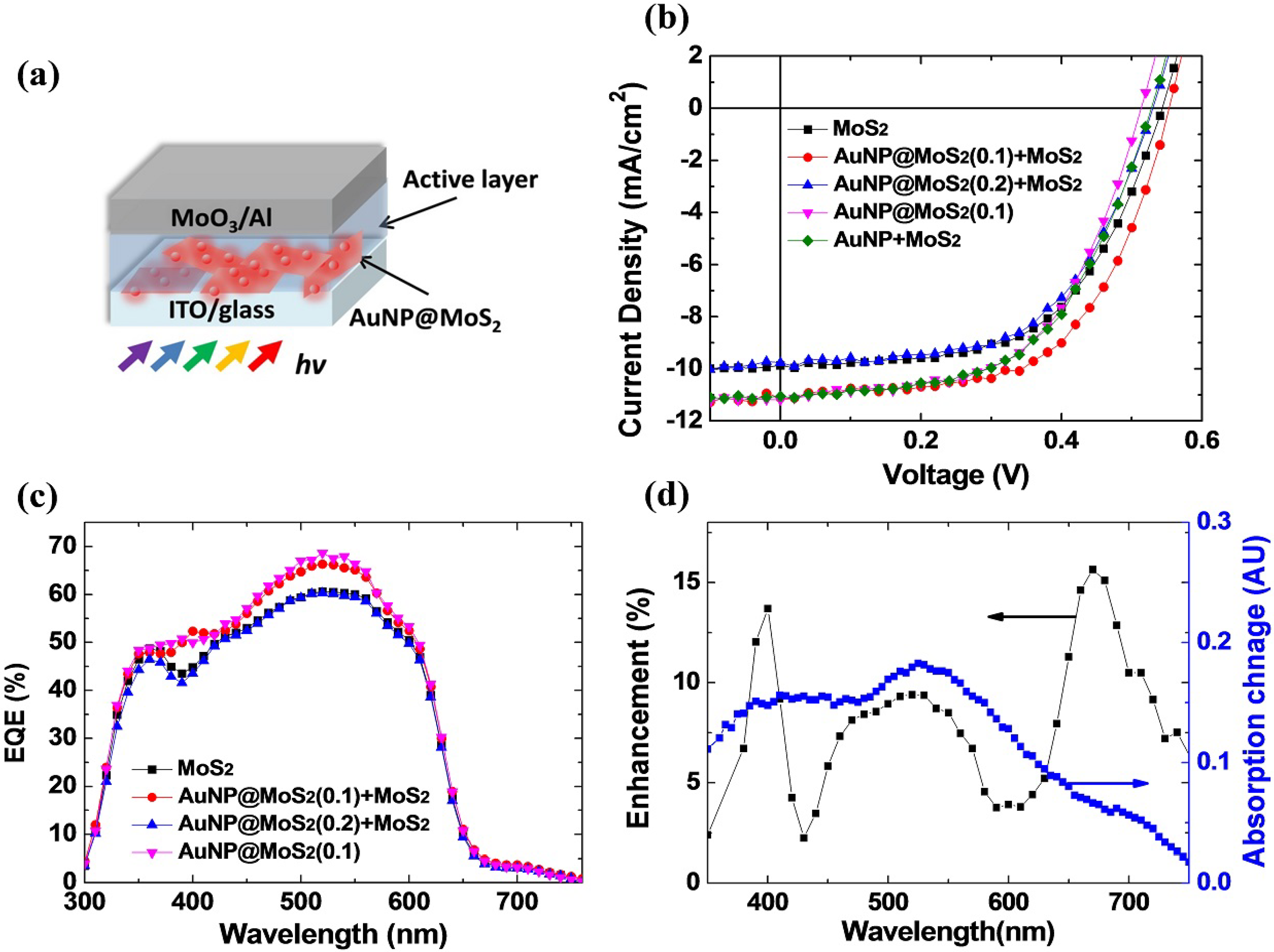
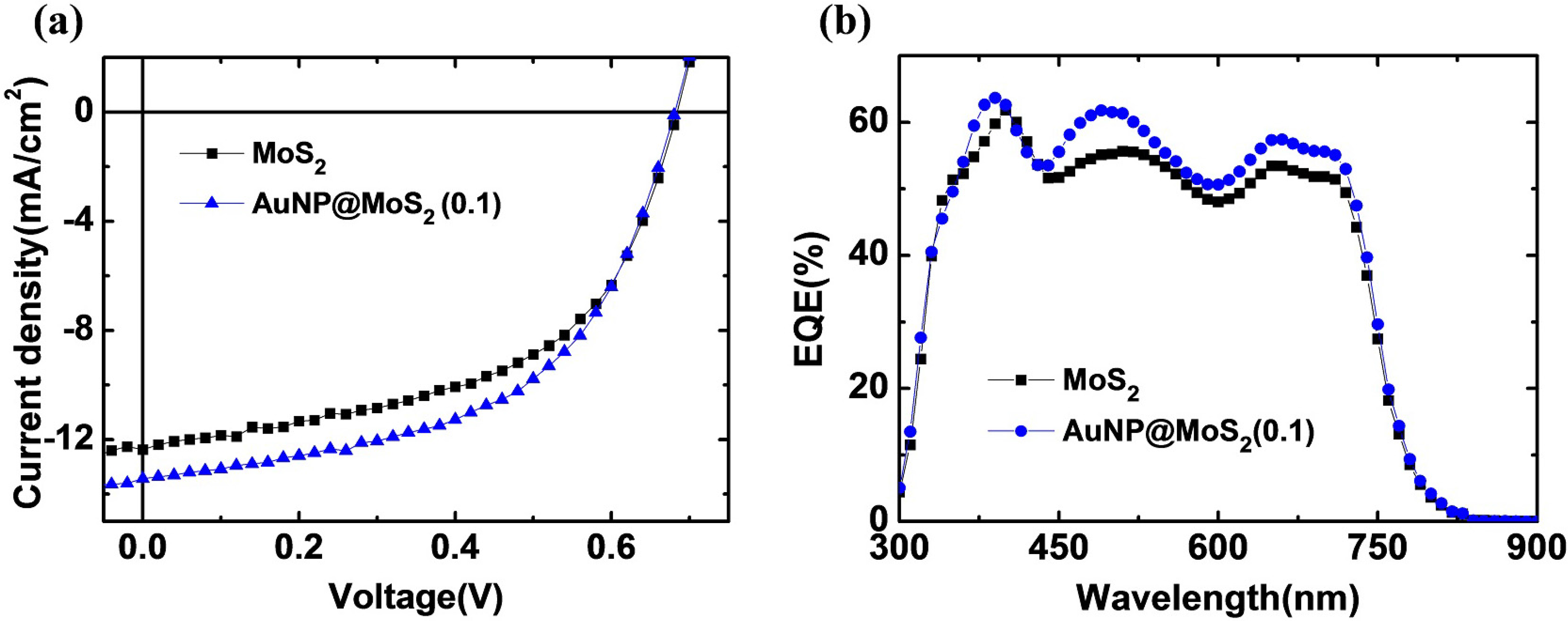
2.2. Photovoltaic Performance of the Devices Prepared with MoS2 Nanocomposites

The as-synthesized MoS2 nanocomposites were used as electrode buffer layers in OPVs. Figure 4a displays the device structure incorporating the MoS2 nanocomposites. Previous reports have inserted MoS2 nanosheets at the anodes [34,35]. Our results, however, indicated that the device using the 2D MoS2 as the cathode buffer layers exhibited better device performance, which is consistence with the data reported by Ibrahem et al. [31]. The different properties of the 2D MoS2 might be due to the different doping levels during the synthesis and device fabrication processes [30,42]. Therefore, we adopted inverted structures to fabricate OPVs with the MoS2 nanocomposites. Figure 4b displays the current density–voltage (J-V) characteristics of the inverted OPVs obtained under illumination with simulated solar light (AM 1.5G); the active layer were P3HT:PCBM blends. Table 1 provides a summary of the electrical properties of the devices in this study. The device prepared with neat MoS2 nanosheets as the cathode buffer exhibited a value of Voc of 0.55 V, a short-circuit current density (Jsc) of 9.87 mA·cm−2, and a fill factor (FF) of 0.56, resulting in a PCE of 3.07%. To investigate the plasmonic effects of these nanocomposites on the performance of OPVs, AuNP@MoS2 nanomaterials were also incorporated at the cathode interface. As revealed in Figure 4b, the direct use of the as-synthesized AuNP@MoS2 composites led to a decrease value of Voc (0.51 V). Although the photocurrent was indeed improved, presumably due to the plasmonic effects, the overall PCE was only slightly improved to 3.19%. We suspected that the density of the Au NPs might be too high, thereby affecting the interfaces between the photoactive polymer blends and the ITO electrodes [18]. Therefore, we further blended neat MoS2 nanosheets into the buffer-layer solution to reduce the amount of Au NPs in the devices. As we can see from Figure 4b, the value of Voc remained unchanged at 0.55 V and both Jsc and FF were improved to 11.1 mA·cm−2 and 0.59, respectively. The calculated PCE was improved to 3.60%. Moreover, if we used the AuNP@MoS2 nanocomposite prepared with higher concentration of Au ions (0.2 mg·mL−1), the device performance started to degraded; both Voc and Jsc were reduced, yielding a lower PCE of 2.97%. From the TEM image (Figure 2c), we infer that the aggregated Au NPs probably degraded the cathode interface and the excess Au NPs might also cause strong back scattering. Figure 4b also displays the J-V curve of the device prepared with the physical mixing buffer solution as we described in the absorption spectra (Figure 1). The device exhibited a value of Voc of 0.53 V, a Jsc of 11.1 mA·cm−2, and a FF of 0.53, resulting in a PCE of 3.21%. The higher photocurrent of the device suggested the present of the plasmonic effects as well [35]. However, the lower value of Voc, which is probably due to the non-optimized density of the Au NPs, led to the inferior performance. We should note that the best concentration of such device might be different from the condition for the devices using AuNP@MoS2 nanocomposite. Further improvement should be still possible after careful optimization of the experimental conditions.
Table 1. Electrical characteristics of devices fabricated with MoS2 and AuNP@MoS2 nanocomposites under various conditions.
Device (concn. of Au ions, mg/mL)Voc (V)Jsc (mA·cm−2)FFPCE (%)
MoS2 a0.55 ± 0.019.87 ± 0.070.56 ± 0.013.07 ± 0.04
AuNP@MoS2(0.10) a0.51 ± 0.0111.2 ± 0.160.56 ± 0.013.19 ± 0.08
AuNP@MoS2(0.10) + MoS2 a0.55 ± 0.0111.1 ± 0.110.59 ± 0.013.60 ± 0.07
AuNP@MoS2(0.20) + MoS2 a0.53 ± 0.019.85 ± 0.060.57 ± 0.012.97 ± 0.05
MoS2 b0.69 ± 0.0112.1 ± 0.100.52 ± 0.014.41 ± 0.06
AuNP@MoS2(0.10) + MoS2 b0.69 ± 0.0113.4 ± 0.120.53 ± 0.014.91 ± 0.07
Notes: a: Photoactive materials: P3HT and PC61BM; b: Photoactive materials: PBDTTT-CT and PC71BM.
To further investigate the origin of the device enhancement, we measured the external quantum efficiency (EQE) spectra (Figure 4c). The EQE values improved for the device prepared with the AuNP@MoS2 nanocomposite, consistent with the previous J-V characteristics. Especially, the efficiencies increased in the wavelength region from 450 to 600 nm, which is consistent with the plasmonic resonance of the Au NPs as shown in Figure 1. The enhancement factor of the plasmonic device compared to the reference MoS2 device was further plotted in Figure 4d. The change in the absorption after the AuNP@MoS2 nanocomposite was incorporated was also presented for easy comparison. We could also observe both enhancements in EQE values and absorption in the spectral the region ranging from 350 to 450 nm. The results were consistent with previous reports [35]. Although no direct plasmonic resonance of the Au NPs located in this spectral region, the absorption of the devices was still increased possibly due to the scattering effects. Similarly, an enhancement peak could be also observed in the 650–750 nm regions. These spectral features indicated that the scattering scheme also contributed to the device enhancements. Therefore, the EQE spectra indicate that the LSPR of the AuNP@MoS2 nanocomposites was responsible for the improved device performance.
Figure 4. (a) The schematic representation of the device structure in this work; (b) J-V curves of the organic photovoltaic devices (OPVs) prepared with various MoS2 nanocomposites; (c) Corresponding external quantum efficiency (EQE) curves of these devices; (d) The calculated EQE enhancement of the device prepared with the AuNP@MoS2 nanocomposites. The change in the absorption spectra after the AuNP@MoS2 nanocomposite was also presented for easy comparison.
Materials 08 05252 g004
To evaluate the potential LSPR effects of the AuNP@MoS2 nanocomposites for various OPV applications, we also applied a low-band-gap polymer to fabricate OPVs. For example, a polymer blend consisting of poly{[4,8-bis-(2-ethyl-hexyl-thiophene-5-yl)-benzo[1,2-b:4,5-b′]dithiophene-2,6-diyl]-alt-[2-(2′-ethyl-hexanoyl)-thieno[3,4-b]thiophen-4,6-diyl]} (PBDTTT-CT) and (6,6)-phenyl C71-butyric acid methyl ester (PC71BM) was used to form the photoactive films; Figure 5 displays the electrical properties of the devices. The reference device prepared with neat MoS2 nanosheets exhibited a value of Voc of 0.69 V, a value of Jsc of 12.1 mA·cm−2, and a FF of 0.52, yielding a calculated PCE of 4.41%. The PCE value was lower than those reported in the literature [43]. Further improvement might be obtained after some solvent additives, such as 1,8-Diiodooctane, are added in the processing solvent. After the surface of MoS2 nanosheets were decorated with Au NPs, the value of Jsc was improved significantly to 13.4 mA·cm−2, while the value of Voc remained unchanged, causing the PCE to increase to 4.91%. Figure 5b displays the corresponding EQE spectra. The EQE values also revealed a similar trend with the photocurrent, suggesting that the AuNP@MoS2 nanocomposites could indeed improve the light harvesting ability. Notably, the EQE values in the spectral range from 600 to 700 nm were also improved. The origin of the EQE enhancement in this wavelength range is still not clear yet and further investigation is required. However, we suspect that it might be due to the coupling between the plasmonic field of the Au NPs and the MoS2 nanosheets as we described previously [36]. Such interesting properties might assist in harvesting the broadband absorption of the solar irradiation.
Figure 5. (a) J-V curves of the OPVs prepared with various MoS2 nanocomposites; (b) Corresponding EQE curves of these devices. Note that the photoactive material of these OPVs were PBDTTT-CT and PC71BM.
Materials 08 05252 g005

3. Experimental Section

For the synthesis of the MoS2 nanocomposites, a 10 mL 1% w/w suspension of bulk MoS2 (Sigma-Aldrich, St. Louis, MO, USA) in DI water was prepared in the first place. Then an aqueous solution of Pluronic P123 (10 wt %; 1.0 mL) (Sigma-Aldrich, St. Louis, MO, USA) was dropped into the MoS2 suspension. The feed ratio of Pluronic P123 was 20:70:20 (EO:PO:EO) and its average Mn was ca. 5.8 kDa. Subsequently, the MoS2 blend was sonicated at room temperature for 17 h [36]. After sonication, the as-prepared MoS2 solution was washed by toluene to remove P123. Then the MoS2 nanosheets were dried through lyophilization. For the preparation of AuNP@MoS2 nanocomposites, the dried MoS2 nanosheets were dispersed in DI water; the concentration was 0.275 mg·mL−1. An aqueous HAuCl4 solution (0.1 or 0.2 mg·mL−1) (Sigma-Aldrich, St. Louis, MO, USA) was added to the MoS2 suspension with a volume ratio of 3:1, respectively. After the spontaneous redox reaction, the resulting suspension was centrifuged, and the residue was washed with toluene and water, respectively. Finally, the nanomaterials were dried through lyophilization.
The devices were prepared on patterned ITO-coated glass substrates. Aqueous solutions of MoS2 or AuNP@MoS2 (0.07 mg·mL−1) were spin-coated onto the ITO substrates and then the sample was baked at 150 °C for 20 min. The photoactive layer, prepared from either a blend of P3HT and PCBM (1:1, w/w) or a blend of PBDTTT-CT and PC70BM (1:1.5, w/w) in 1,2-dichlorobenzene, was spin-coated onto the MoS2 or AuNP@MoS2 layers. The photoactive film underwent solvent annealing in a glass Petri dish [44]. Then, the sample was thermally annealed at 110 °C for 15 min. Finally, the device was completed through thermal evaporation of MoO3 (3 nm) and Al (100 nm) as the anode. The electrical characteristics of the devices were measured using a Keithley 2400 source-measure unit (Keithley Instruments, Cleveland, OH, USA). A 150-W Thermal Oriel solar simulator (AM 1.5G) was used as the light source druing the meansuremnts. The intensity of the light source was calibrated using a standard Si photodiode equipped with a KG5 filter. The EQE spectra were obtained using a QE measurement system (Enli Technology, Kaohsiung, Taiwan). The absorption spectra were recorded using a UV-Vis-NIR spectrometer (PerkinElmer Lambda 950, Waltham, UK). Raman spectra were acquired using a Horoba high-resolution confocal Raman microscope (HORIBA Scientific, Kyoto, Japan) equipped with a green laser (532 nm) as the light source.

4. Conclusions

We have synthesized AuNP@MoS2 nanocomposites that could improve the efficiency of OPVs. The AuNP@MoS2 nanocomposites were prepared through a simple spontaneous redox reaction between Au ions and MoS2 nanosheets. The nanocomposite functioned as the cathode buffer layers and introduced LSPR effects in the devices, thereby resulting in noticeable enhancements in the photocurrent and the PCEs of the OPVs. Moreover, our results reveal the existence of possible coupling of plasmonic resonance between the Au NPs and the MoS2 nanosheets, which might be helpful for extending the spectral range of enhanced photon absorption. We anticipate that these results will open up new avenues for improving the performance of OPVs through the exploitation of plasmonic effects in 2D nanomaterials.

Acknowledgments

We thank the Ministry of Science and Technology (Grant Nos.: MOST 103-2923-E-009-001-MY3, MOST 102-2221-E-009-130-MY3 and MOST 101-2628-E-009-008-MY3) and the Ministry of Education of Taiwan (through the ATU program) for financial support.

Author Contributions

Ming-Kai Chuang and Shun-Shing Yang synthesized the nanocomposites and fabricated and characterized the OPVs. Ming-Kai Chuang and Fang-Chung Chen discussed the experiments and wrote the manuscript. Fang-Chung Chen supervised the project.

Conflicts of Interest

The authors declare no conflict of interest.

References

  1. Dennler, G.; Scharber, M.C.; Brabec, C.J. Polymer-fullerene bulk-heterojunction solar cells. Adv. Mater. 2009, 13, 1323–1328. [Google Scholar] [CrossRef]
  2. Dou, L.; You, J.; Hong, Z.; Xu, Z.; Li, G.; Street, R.A.; Yang, Y. A decade of organic/polymeric photovoltaic research. Adv. Mater. 2013, 25, 6642–6671. [Google Scholar] [CrossRef] [PubMed]
  3. Yip, H.L.; Jen, A.K.-Y. Recent Advances in Solution-processed interfacial materials for efficient and stable polymer solar cells. Energy Environ. Sci. 2012, 5, 5994–6011. [Google Scholar] [CrossRef]
  4. Li, G.; Zhu, R.; Yang, Y. Polymer solar cells. Nat. Photonics 2012, 6, 153–161. [Google Scholar] [CrossRef]
  5. Park, S.H.; Roy, A.; Beaupré, S.; Cho, S.; Coates, N.; Moon, J.S.; Moses, D.; Leclerc, M.; Lee, K.; Heeger, A.J. Bulk heterojunction solar cells with internal quantum efficiency approaching 100%. Nat. Photonics 2012, 6, 297–303. [Google Scholar]
  6. Ko, D.H.; Tumbleston, J.R.; Gadisa, A.; Aryal, M.; Liu, Y.; Lopez, R.; Samulski, E.T. Light-trapping nano-structures in organic photovoltaic cells. J. Mater. Chem. 2011, 21, 16293–16303. [Google Scholar] [CrossRef]
  7. Kim, J.Y.; Kim, S.H.; Lee, H.H.; Lee, K.; Ma, W.; Gong, X.; Heeger, A.J. New architecture for high-efficiency polymer photovoltaic cells using solution-based titanium oxide as an optical spacer. Adv. Mater. 2006, 18, 572–576. [Google Scholar] [CrossRef]
  8. Chen, F.C.; Wu, J.L.; Hung, Y. Spatial redistribution of the optical field intensity in inverted polymer solar cells. Appl. Phys. Lett. 2010, 96. [Google Scholar] [CrossRef]
  9. Tumbleston, J.R.; Ko, D.H.; Samulski, E.T.; Lopez, R. Absorption and quasiguided mode analysis of organic solar cells with photonic crystal photoactive layers. Opt. Express 2009, 17, 7670–7681. [Google Scholar] [CrossRef] [PubMed]
  10. Gan, Q.; Bartoli, F.J.; Kafafi, Z.H. Plasmonic-enhanced organic photovoltaics: Breaking the 10% efficiency barrier. Adv. Mater. 2013, 25, 2385–2396. [Google Scholar] [CrossRef] [PubMed]
  11. Stratakis, E.; Kymakis, E. Nanoparticle-based plasmonic organic photovoltaic devices. Mater. Today 2013, 16, 133–146. [Google Scholar] [CrossRef]
  12. Chou, C.H.; Chen, F.C. Plasmonic nanostructures for light trapping in organic photovoltaic devices. Nanoscale 2014, 6, 8444–8458. [Google Scholar] [CrossRef] [PubMed]
  13. Hsiao, Y.S.; Charan, S.; Wu, F.Y.; Chien, F.C.; Chu, C.W.; Chen, P.; Chen, F.C. Improving the light trapping efficiency of plasmonic polymer solar cells through photon management. J. Phys. Chem. C 2012, 116, 20731–20737. [Google Scholar] [CrossRef]
  14. Wang, D.H.; Kim, D.Y.; Choi, K.W.; Seo, J.H.; Im, S.H.; Park, J.H.; Park, O.O.; Heeger, A.J. Enhancement of donor–acceptor polymer bulk heterojunction solar cell power conversion efficiencies by addition of Au nanoparticles. Angew. Chem. Int. Ed. 2011, 50, 5519–5523. [Google Scholar] [CrossRef] [PubMed]
  15. Li, X.; Choy, W.C.H.; Lu, H.; Sha, W.E.I.; Ho, A.H.P. Efficiency enhancement of organic solar cells by using shape-dependent broadband plasmonic absorption in metallic nanoparticles. Adv. Funct. Mater. 2013, 21, 2728–2735. [Google Scholar] [CrossRef]
  16. Chen, F.C.; Wu, J.L.; Lee, C.L.; Hung, Y.; Kuo, C.H.; Huang, M.H. Plasmonic-enhanced polymer photovoltaic devices incorporating solution-processable metal nanoparticles. Appl. Phys. Lett. 2009, 95. [Google Scholar] [CrossRef]
  17. Wu, J.L.; Chen, F.C.; Hsiao, Y.S.; Chien, F.C.; Chen, P.; Kuo, C.H.; Huang, M.H.; Hsu, C.S. Surface plasmonic effects of metallic nanoparticles on the performance of polymer bulk heterojunction solar cells. ACS Nano 2011, 5, 959–967. [Google Scholar] [CrossRef] [PubMed]
  18. Chuang, M.K.; Lin, S.W.; Chen, F.C.; Chu, C.W.; Hsu, C.S. Gold Nanoparticle-decorated graphene oxides for plasmonic-enhanced polymer photovoltaic devices. Nanoscale 2014, 6, 1573–1579. [Google Scholar] [CrossRef] [PubMed]
  19. Chuang, M.K.; Chen, F.C. Synergistic plasmonic effects of metal nanoparticle–decorated PEGylated graphene oxides in polymer solar cells. ACS Appl. Mater. Interfaces 2015, 7, 7397–7405. [Google Scholar] [CrossRef] [PubMed]
  20. Wang, D.H.; Park, K.H.; Seo, J.H.; Seifter, J.; Jeon, J.H.; Kim, J.K.; Park, J.H.; Park, O.O.; Heeger, A.J. Enhanced power conversion efficiency in PCDTBT/PC70BM bulk heterojunction photovoltaic devices with embedded silver nanoparticle clusters. Adv. Energy Mater. 2011, 1, 766–770. [Google Scholar] [CrossRef]
  21. Spyropoulos, G.D.; Stylianakis, M.; Stratakis, E.; Kymakis, E. Plasmonic organic photovoltaics doped with metal nanoparticles. Photonics Nanostruct. 2011, 9, 184–189. [Google Scholar] [CrossRef]
  22. Stratakis, E.; Stylianakis, M.M.; Koudoumas, E.; Kymakis, E. Plasmonic organic photovoltaic devices with graphene based buffer layers for stability and efficiency enhancement. Nanoscale 2013, 5, 4144–4150. [Google Scholar] [CrossRef] [PubMed]
  23. Kymakis, E.; Spyropoulos, G.D.; Fernandes, R.; Kakavelakis, G.; Kanaras, G.; Strarakis, E. Plasmonic bulk heterojunction solar cells: The role of nanoparticle ligand coating. ACS Photonics 2015, 2, 714–723. [Google Scholar] [CrossRef]
  24. Jariwala, D.; Sangwan, V.K.; Lauhou, L.J.; Marks, T.J.; Hersam, M.C. Emerging device applications for semiconducting two-dimensional transition metal dichalcogenides. ACS Nano 2014, 8, 1102–1120. [Google Scholar] [CrossRef] [PubMed]
  25. Huang, X.; Zeng, Z.; Zhang, H. Metal dichalcogenide nanosheets: Preparation, properties and applications. Chem. Soc. Rev. 2013, 42, 1934–1946. [Google Scholar] [CrossRef] [PubMed]
  26. Radisavljevic, B.; Radenovic, A.; Brivio, J.; Giacometti, V.; Kis, A. Single-layer MoS2 transistors. Nat. Nanotechnol. 2011, 6, 147–150. [Google Scholar] [CrossRef] [PubMed]
  27. Yin, Z.; Li, H.; Li, H.; Jiang, L.; Shi, Y.; Sun, Y.; Lu, G.; Zhang, Q.; Chen, X.; Zhang, H. Single-layer MoS2 phototransistors. ACS Nano 2012, 6, 74–80. [Google Scholar] [CrossRef] [PubMed]
  28. Sundaram, R.; Engel, M.; Lombardo, A.; Krupke, R.; Ferrari, A.; Avouris, P.; Steiner, M. Electroluminescence in single layer MoS2. Nano Lett. 2013, 13, 1416–1421. [Google Scholar] [CrossRef] [PubMed]
  29. Li, H.; Yin, Z.; He, Q.; Li, H.; Huang, X.; Lu, G.; Fam, D.W.H.; Tok, A.I.Y.; Zhang, Q.; Zhang, H. Fabrication of single-and multilayer MoS2 film-based field-effect transistors for sensing NO at room temperature. Small 2012, 8, 63–67. [Google Scholar] [CrossRef] [PubMed]
  30. Yun, J.M.; Noh, Y.J.; Yeo, J.S.; Go, Y.J.; Na, S.I.; Jeong, H.G.; Kim, J.; Lee, S.; Kim, S.S.; Koo, H.Y.; et al. Efficient work-function engineering of solution-processed MoS2 thin-films for novel hole and electron transport layers leading to high-performance polymer solar cells. J. Mater. Chem. C 2013, 1, 3777–3783. [Google Scholar] [CrossRef]
  31. Ibrahem, M.A.; Lan, T.; Huang, J.K.; Chen, Y.Y.; Wei, K.H.; Li, L.J.; Chu, C.W. High quantity and quality few-layers transition metal disulfide nanosheets from wet-milling exfoliation. RSC Adv. 2013, 3, 13193–13202. [Google Scholar] [CrossRef]
  32. Gu, X.; Cui, W.; Li, H.; Wu, Z.; Zeng, Z.; Lee, S.T.; Zhang, H.; Sun, B. A solution-processed hole extraction layer made from ultrathin MoS2 nanosheets for efficient organic solar cells. Adv. Energy Mater. 2013, 3, 1262–1268. [Google Scholar] [CrossRef]
  33. Yang, X.; Fu, W.; Liu, W.; Hong, J.; Cai, Y.; Jin, C.; Xu, M.; Wang, H.; Yang, D.; Chen, H. Engineering crystalline structures of two dimensional MoS2 sheets for high-performance organic solar cells. J. Mater. Chem. A 2014, 2, 7727–7733. [Google Scholar] [CrossRef]
  34. Liu, W.; Yang, X.; Zhang, Y.; Xu, M.; Chen, H. Ultra-stable two-dimensional MoS2 solution for highly efficient organic solar cells. RSC Adv. 2014, 4, 32744–32748. [Google Scholar] [CrossRef]
  35. Yang, X.; Liu, W.; Xiong, M.; Zhang, Y.; Liang, T.; Yang, J.; Xu, M.; Ye, J.; Chen, H. Au nanoparticles on ultrathin MoS2 sheets for plasmonic organic solar cells. J. Mater. Chem. A 2014, 2, 14798–14806. [Google Scholar] [CrossRef]
  36. Quinn, M.D.J.; Ho, N.H.; Notley, S.M. Aqueous dispersions of exfoliated molybdenum disulfide for use in visible-light photocatalysis. ACS Appl. Mater. Interfaces 2013, 5, 12751–12756. [Google Scholar] [CrossRef] [PubMed]
  37. Kim, J.; Byun, S.; Smith, A.J.; Yu, J.; Huang, J. Enhanced electrocatalytic properties of transition-metal dichalcogenides sheets by spontaneous gold nanoparticle decoration. J. Phys. Chem. Lett. 2013, 4, 1227–1232. [Google Scholar] [CrossRef]
  38. Yadgarov, L.; Choi, C.L.; Sedova, A.; Cohen, A.; Rosentsveig, R.; Bar-Elli, O.; Oron, D.; Dai, H.; Tenne, R. Dependence of the absorption and optical surface plasmon scattering of MoS2 nanoparticles on aspect ratio, size, and media. ACS Nano 2014, 8, 3575–3583. [Google Scholar] [CrossRef] [PubMed]
  39. Wang, Y.; Ou, J.Z.; Balendhran, S.; Chrimes, A.F.; Mortazavi, M.; Yao, D.D.; Field, M.R.; Latham, K.; Bansal, V.; Friend, J.R.; et al. Electrochemical control of photoluminescence in two-dimensional MoS2 nanoflakes. ACS Nano 2013, 7, 10083–10093. [Google Scholar] [CrossRef] [PubMed]
  40. Polyakov, A.Y.; Yadgatov, L.; Popovita-biro, R.; Lebedev, V.A.; Pinkas, I.; Rosentsveig, R.; Feldman, Y.; Goldt, A.E.; Goodilin, E.A.; Tenne, R. Decoration of WS2 nanotubes and fullerene-like MoS2 with gold nanoparticles. J. Phys. Chem. C 2014, 118, 2161–2169. [Google Scholar] [CrossRef]
  41. Li, H.; Zhang, Q.; Tap, C.C.R.; Tay, B.K.; Edwin, T.H.T.; Olivier, A.; Baillargeat, D. From bulk to monolayer MoS2: Evolution of Raman scattering. Adv. Funct. Mater. 2012, 22, 1385–1390. [Google Scholar] [CrossRef]
  42. Fang, H.; Tosun, M.; Seol, G.; Chang, T.C.; Takei, K.; Guo, J.; Javey, A. Degenerate n-doping of few-layer transition metal dichalcogendies by potassium. Nano Lett. 2013, 13, 1991–1995. [Google Scholar] [CrossRef] [PubMed]
  43. Guo, X.; Zhang, M.; Ma, W.; Ye, L.; Zhang, S.; Liu, S.; Ade, H.; Huang, F.; Hou, J. Enhanced photovoltaic performance by modulating surface composite in bulk heterojunction polymer solar cells based on PBDTTT-C-T/PC71BM. Adv. Mater. 2014, 26, 4043–4049. [Google Scholar] [CrossRef] [PubMed]
  44. Chen, F.C.; Ko, C.J.; Wu, J.L.; Chen, W.C. Morphological study of P3HT:PCBM blend films prepared through solvent annealing for solar cell applications. Sol. Energy Mater. Sol. Cells 2010, 94, 2426–2430. [Google Scholar] [CrossRef]

