Fabrication of Micro- and Nanopillars from Pyrolytic Carbon and Tetrahedral Amorphous Carbon

 , , , and
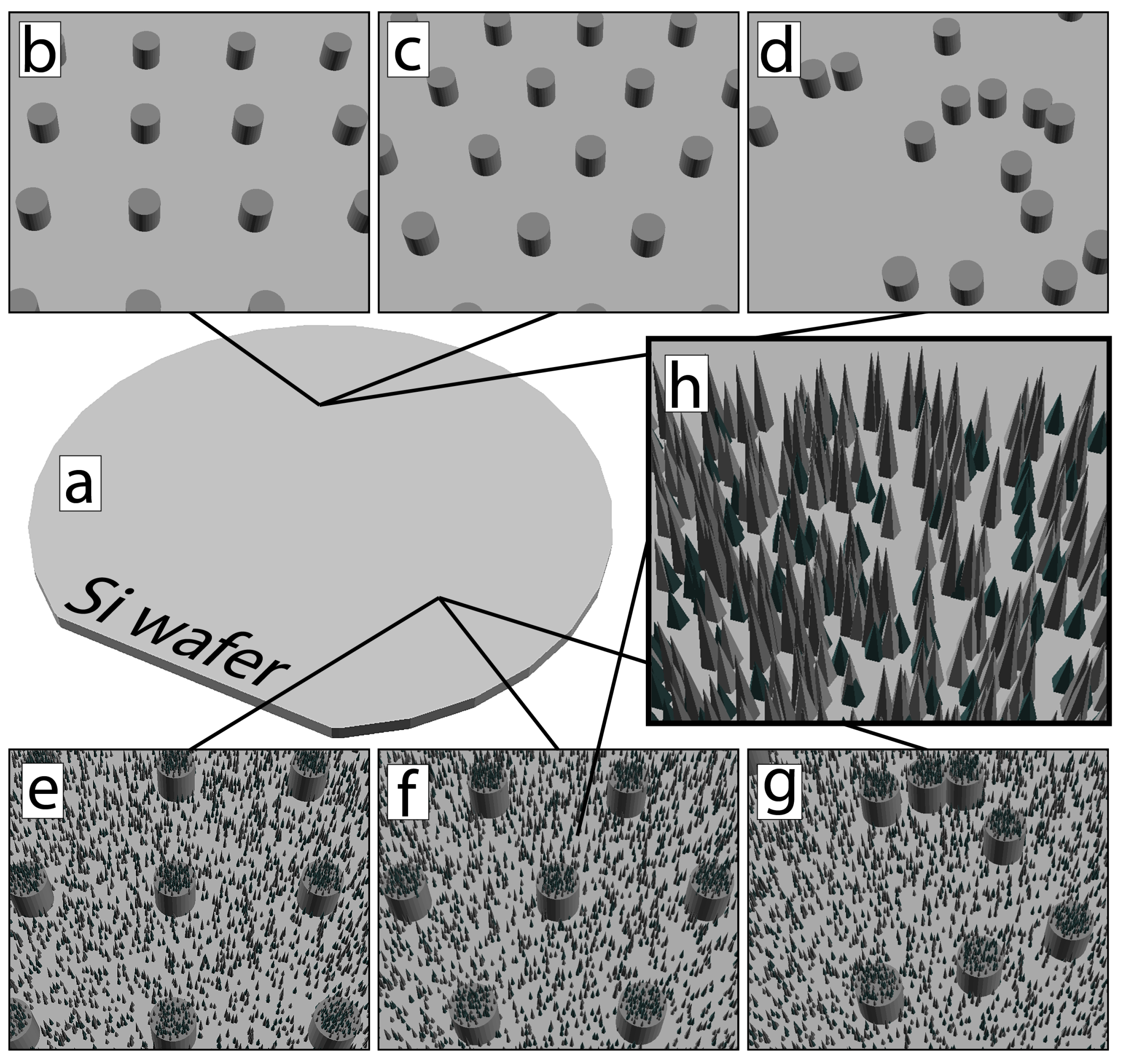
Abstract
:1. Introduction
2. Experimental
2.1. Pyrolyzed Carbon Sample Fabrication
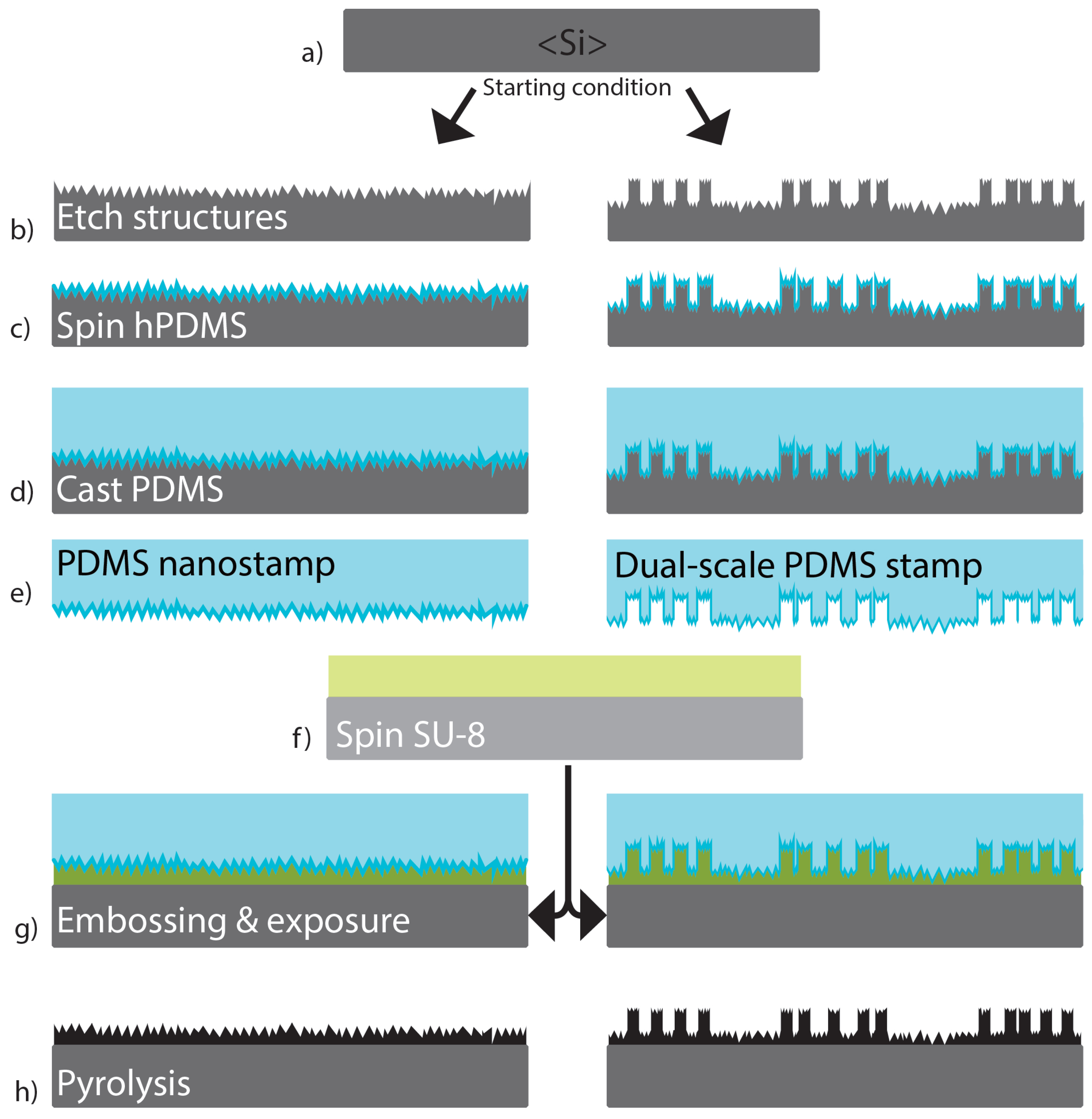
2.1.1. Silicon Master
2.1.2. hPDMS-PDMS Stamp
2.1.3. SU-8 Processing
2.1.4. Dicing
2.1.5. Pyrolysis
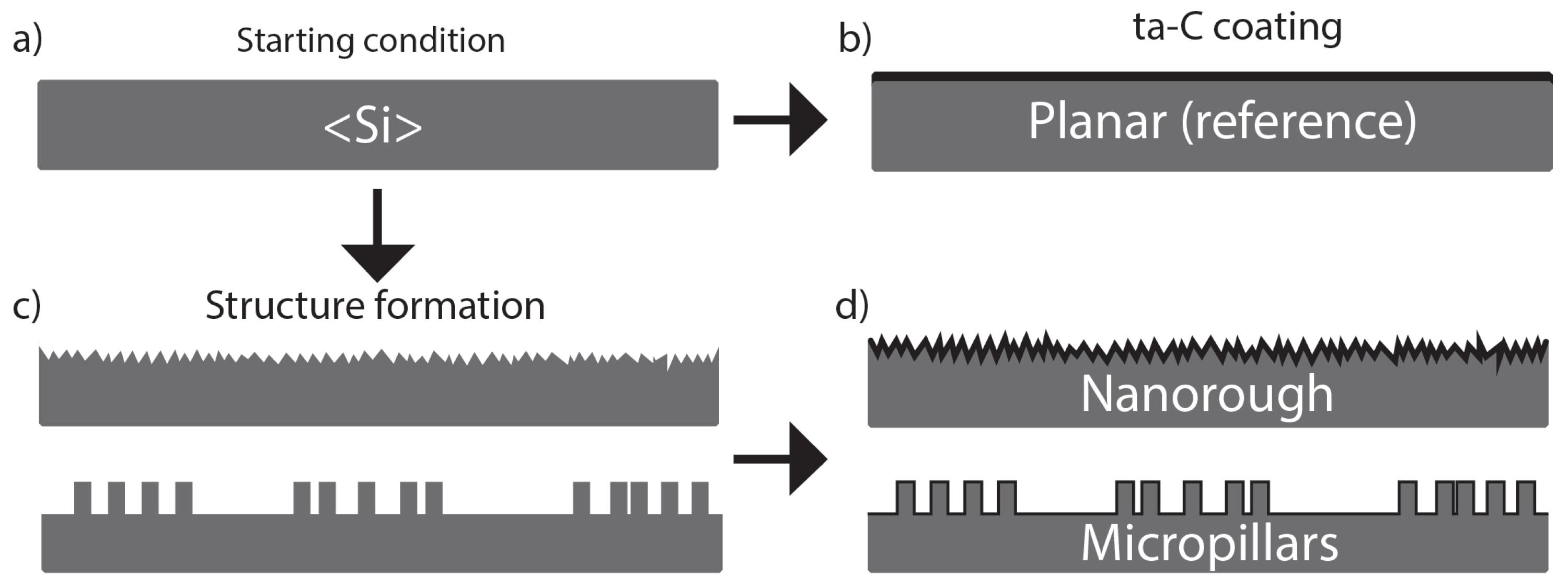
2.2. ta-C Sample Fabrication
2.3. Cell Cultures
3. Results and Discussion
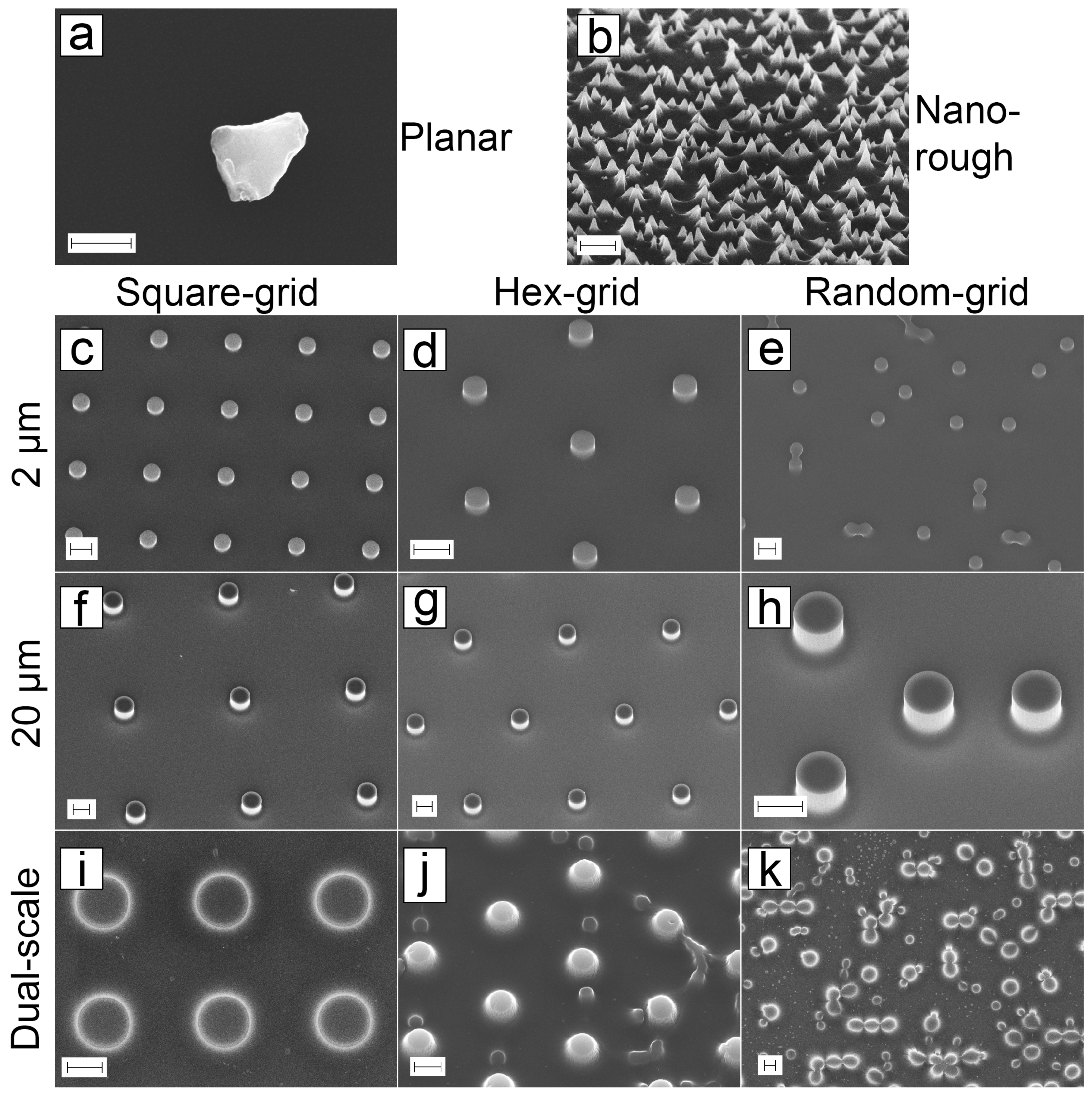
3.1. PyC Structures
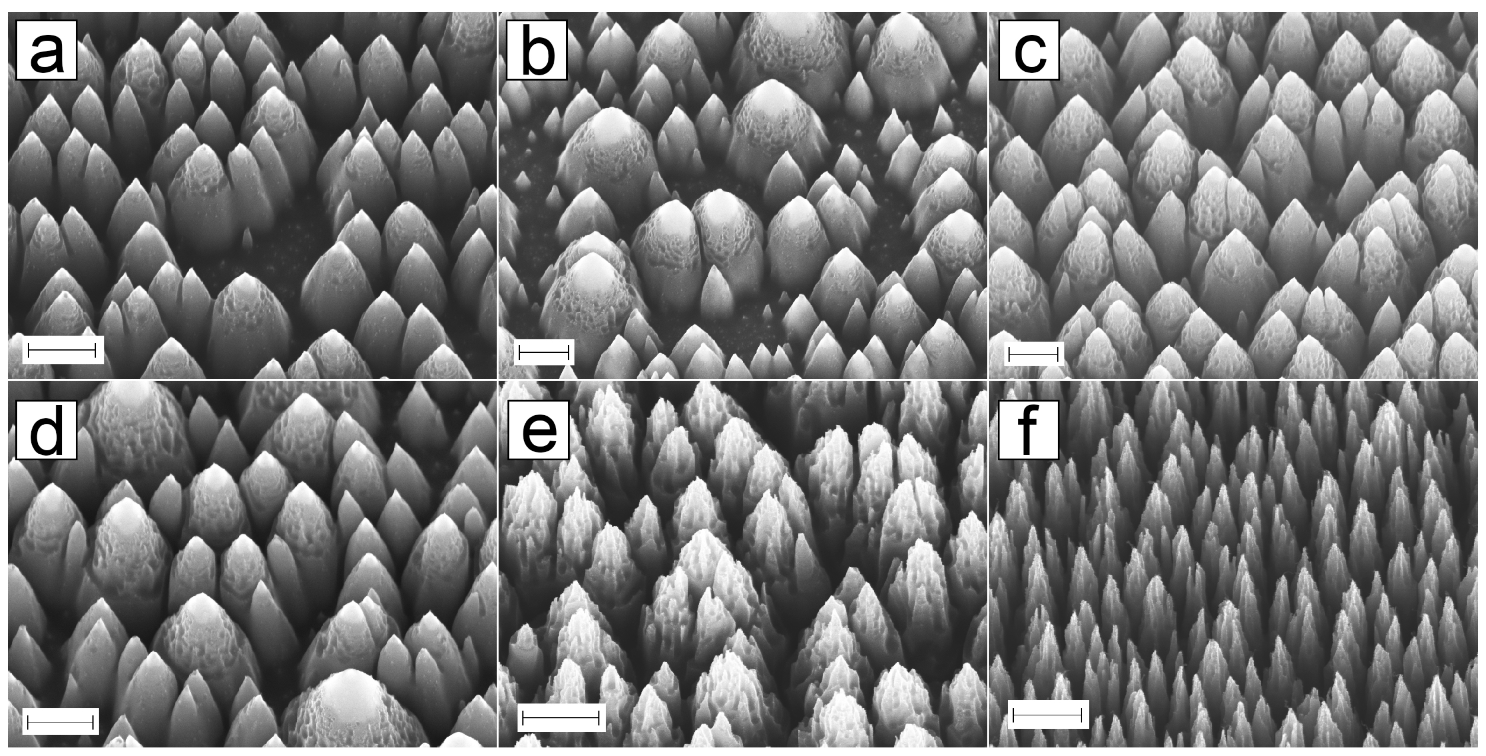
3.1.1. Black Silicon Profile Optimization for Replication
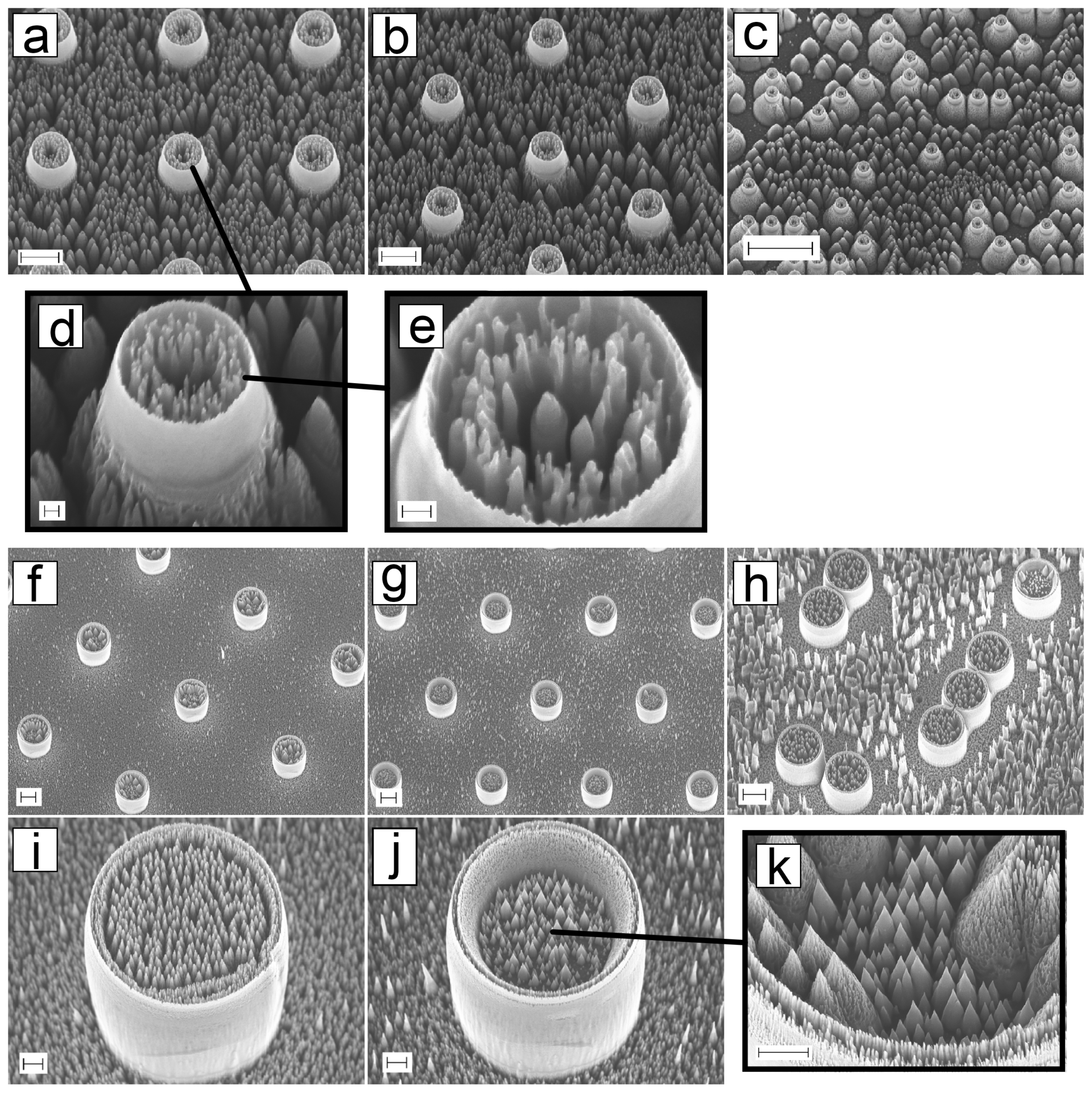
3.1.2. Dual-Scale Micro- and Nanopillars
3.1.3. SU-8 Embossing
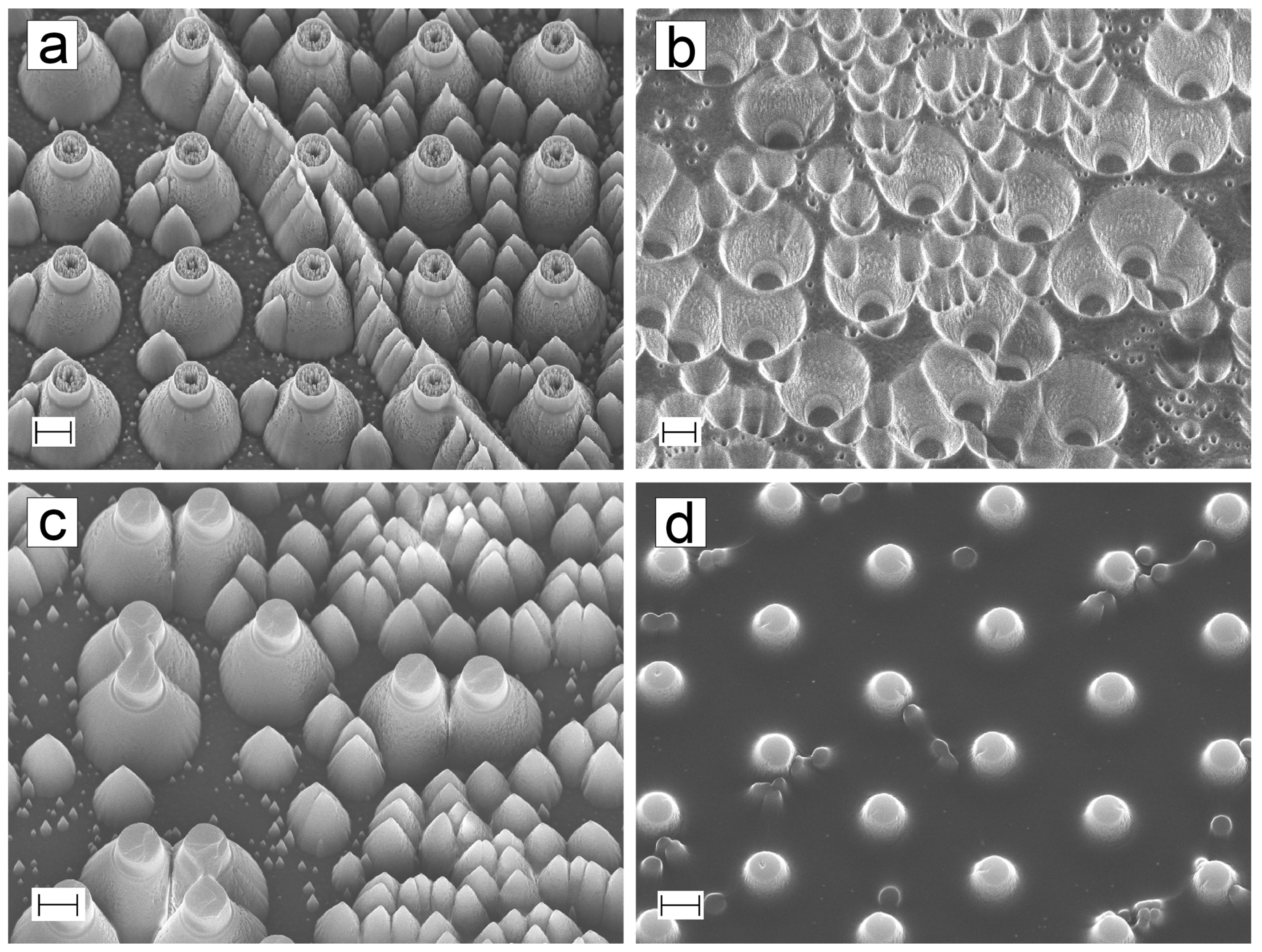
3.1.4. Pyrolysis
3.1.5. Shrinkage
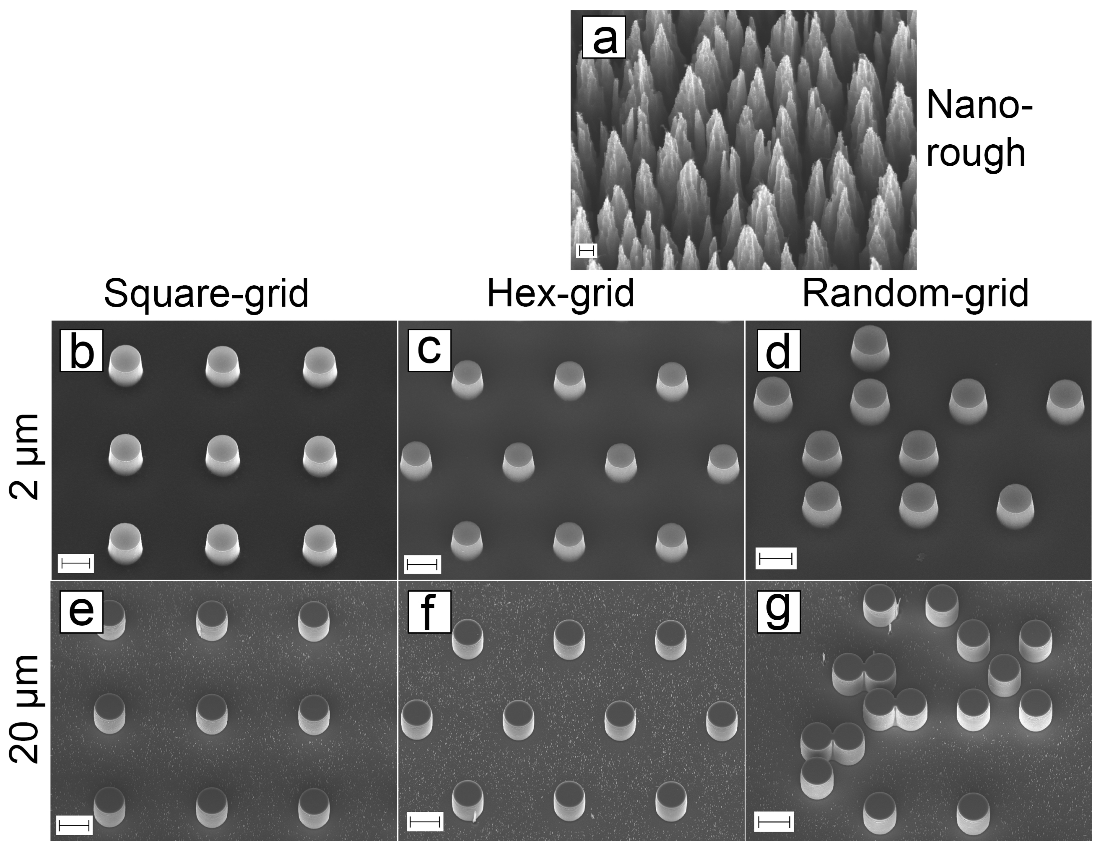
3.2. ta-C Structures
3.3. Fabrication Comparison
3.4. Cell Compatibility
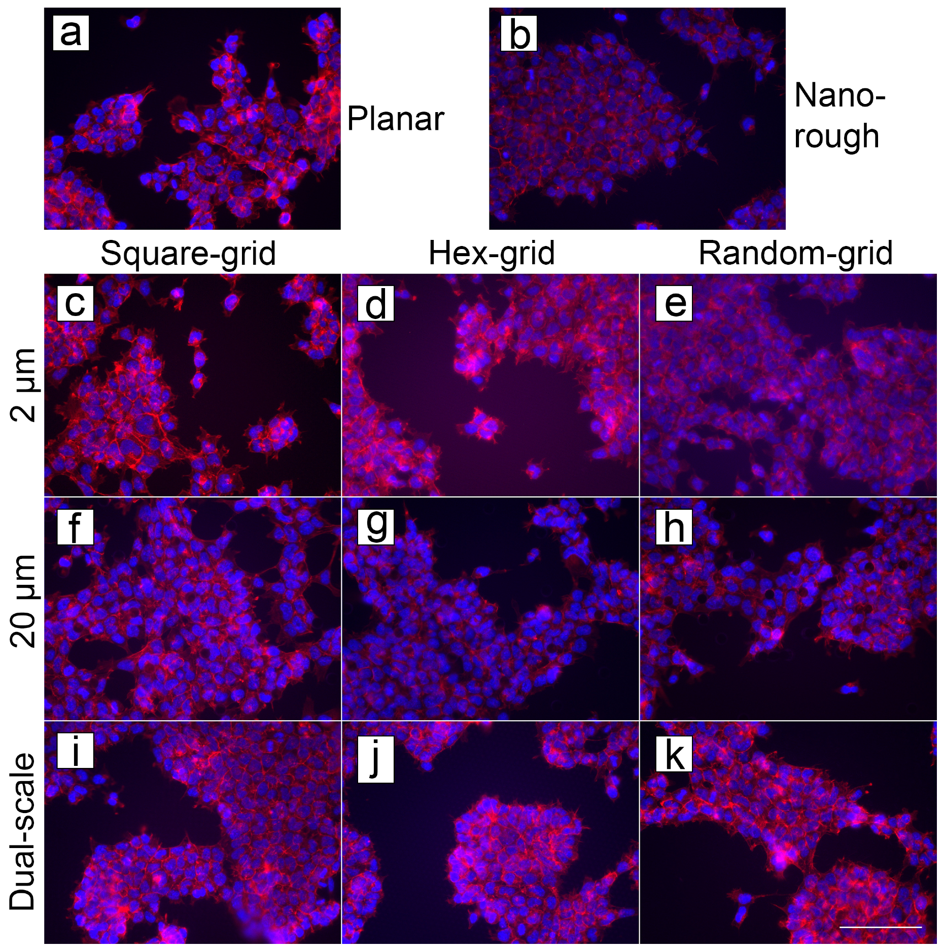
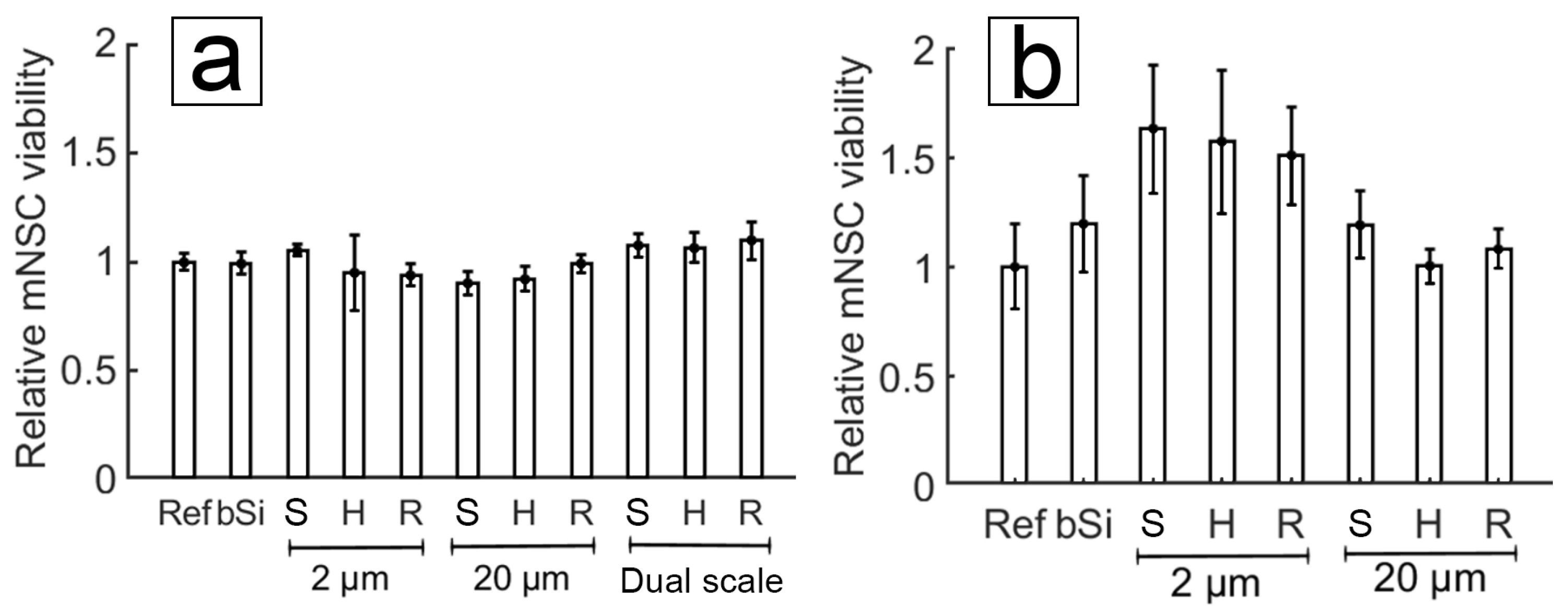
3.4.1. Cell Cultures on PyC
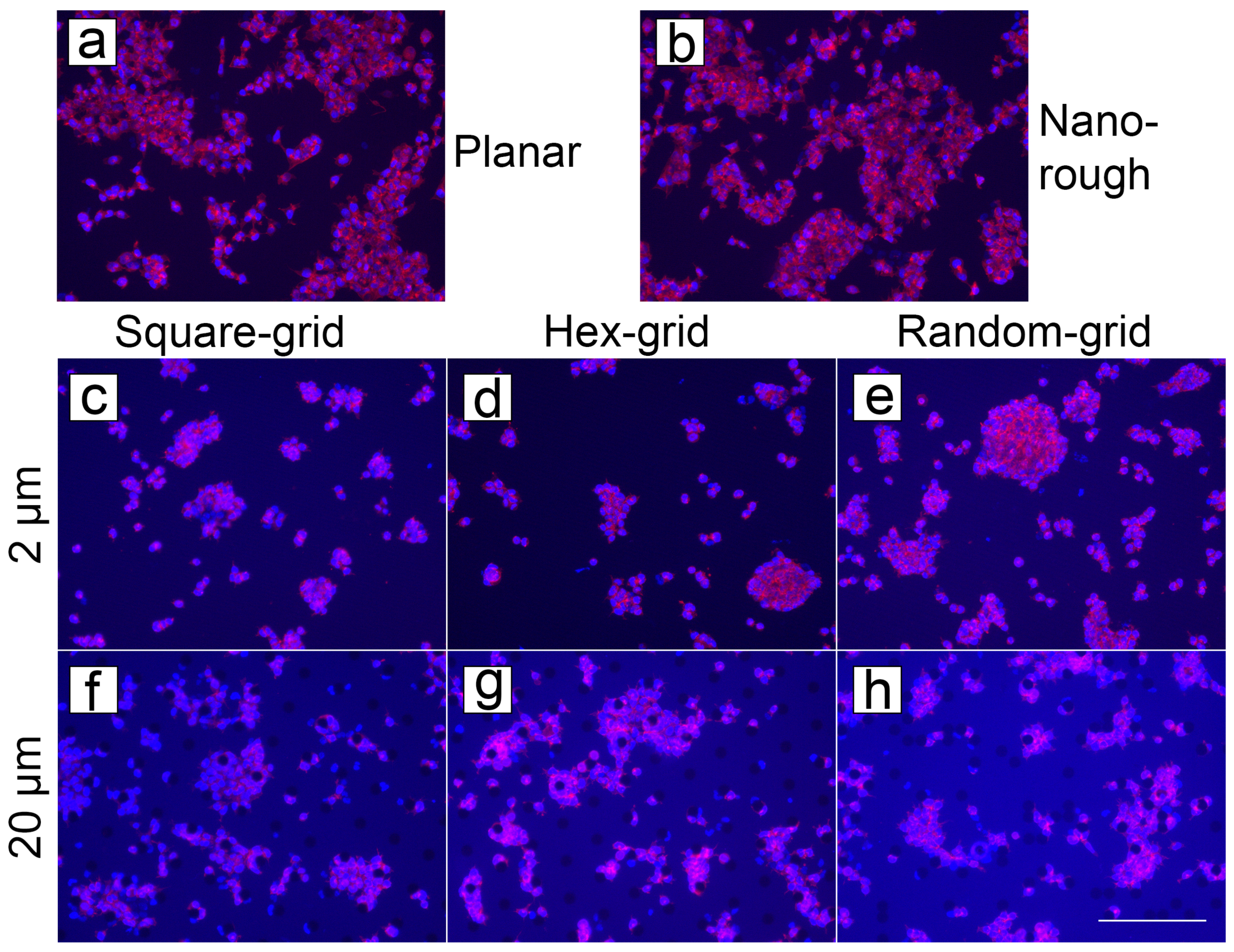
3.4.2. Cell Cultures on ta-C
3.4.3. Comparison
4. Conclusions
Author Contributions
Funding
Acknowledgments
Conflicts of Interest
References
- Aisenberg, S.; Chabot, R. Ion-beam deposition of thin films of diamondlike carbon. J. Appl. Phys. 1971, 42, 2953–2958. [Google Scholar] [CrossRef]
- Robertson, J. Diamond-like amorphous carbon. Mater. Sci. Eng. R Rep. 2002, 37, 129–281. [Google Scholar] [CrossRef] [Green Version]
- Grill, A. Diamond-like carbon coatings as biocompatible materials—An overview. Diam. Relat. Mater. 2003, 12, 166–170. [Google Scholar] [CrossRef]
- Charitidis, C. Nanomechanical and nanotribological properties of carbon-based thin films: A review. Int. J. Refract. Met. Hard Mater. 2010, 28, 51–70. [Google Scholar] [CrossRef]
- Mitura, E.; Mitura, S.; Niedzielski, P.; Has, Z.; Wolowiec, R.; Jakubowski, A.; Szmidt, J.; Sokołowska, A.; Louda, P.; Marciniak, J.; et al. Diamond-like carbon coatings for biomedical applications. Diam. Relat. Mater. 1994, 3, 896–898. [Google Scholar] [CrossRef]
- Lettington, A.H. Applications of diamond-like carbon thin films. Carbon 1998, 36, 555–560. [Google Scholar] [CrossRef]
- Loir, A.S.; Garrelie, F.; Donnet, C.; Belin, M.; Forest, B.; Rogemond, F.; Laporte, P. Deposition of tetrahedral diamond-like carbon thin films by femtosecond laser ablation for applications of hip joints. Thin Solid Films 2004, 453, 531–536. [Google Scholar] [CrossRef]
- Narayan, R.J. Nanostructured diamondlike carbon thin films for medical applications. Mater. Sci. Eng. C 2005, 25, 405–416. [Google Scholar] [CrossRef]
- Schnupp, R.; Kühnhold, R.; Temmel, G.; Burte, E.; Ryssel, H. Thin carbon films as electrodes for bioelectronic applications. Biosens. Bioelectron. 1998, 13, 889–894. [Google Scholar] [CrossRef]
- Maalouf, R.; Chebib, H.; Saikali, Y.; Vittori, O.; Sigaud, M.; Garrelie, F.; Donnet, C.; Jaffrezic-Renault, N. Characterization of different diamond-like carbon electrodes for biosensor design. Talanta 2007, 72, 310–314. [Google Scholar] [CrossRef]
- Tujunen, N.; Kaivosoja, E.; Protopopova, V.; Valle-Delgado, J.J.; Österberg, M.; Koskinen, J.; Laurila, T. Electrochemical detection of hydrogen peroxide on platinum-containing tetrahedral amorphous carbon sensors and evaluation of their biofouling properties. Mater. Sci. Eng. C 2015, 55, 70–78. [Google Scholar] [CrossRef] [PubMed] [Green Version]
- Peltola, E.; Wester, N.; Holt, K.B.; Johansson, L.S.; Koskinen, J.; Myllymäki, V.; Laurila, T. Nanodiamonds on tetrahedral amorphous carbon significantly enhance dopamine detection and cell viability. Biosens. Bioelectron. 2017, 88, 273–282. [Google Scholar] [CrossRef] [PubMed] [Green Version]
- Peltola, E.; Sainio, S.; Holt, K.B.; Palomäki, T.; Koskinen, J.; Laurila, T. Electrochemical fouling of dopamine and recovery of carbon electrodes. Anal. Chem. 2017, 90, 1408–1416. [Google Scholar] [CrossRef] [PubMed]
- Isoaho, N.; Peltola, E.; Sainio, S.; Wester, N.; Protopopova, V.; Wilson, B.P.; Koskinen, J.; Laurila, T. Carbon nanostructure based platform for enzymatic glutamate biosensors. J. Phys. Chem. C 2017, 121, 4618–4626. [Google Scholar] [CrossRef]
- Palomäki, T.; Peltola, E.; Sainio, S.; Wester, N.; Pitkänen, O.; Kordas, K.; Koskinen, J.; Laurila, T. Unmodified and multi-walled carbon nanotube modified tetrahedral amorphous carbon (ta-C) films as in vivo sensor materials for sensitive and selective detection of dopamine. Biosens. Bioelectron. 2018, 118, 23–30. [Google Scholar] [CrossRef] [PubMed]
- Martinez-Duarte, R. SU-8 Photolithography as a Toolbox for Carbon MEMS. Micromachines 2014, 5, 766–782. [Google Scholar] [CrossRef]
- Keeley, G.P.; McEvoy, N.; Nolan, H.; Kumar, S.; Rezvani, E.; Holzinger, M.; Cosnier, S.; Duesberg, G.S. Simultaneous electrochemical determination of dopamine and paracetamol based on thin pyrolytic carbon films. Anal. Methods 2012, 4, 2048–2053. [Google Scholar] [CrossRef]
- Amato, L.; Heiskanen, A.; Caviglia, C.; Shah, F.; Zór, K.; Skolimowski, M.; Madou, M.; Gammelgaard, L.; Hansen, R.; Seiz, E.G.; et al. Pyrolysed 3D-Carbon Scaffolds Induce Spontaneous Differentiation of Human Neural Stem Cells and Facilitate Real-Time Dopamine Detection. Adv. Funct. Mater. 2014, 24, 7042–7052. [Google Scholar] [CrossRef]
- Peltola, E.; Heikkinen, J.J.; Sovanto, K.; Sainio, S.; Aarva, A.; Franssila, S.; Jokinen, V.; Laurila, T. SU-8 based pyrolytic carbon for the electrochemical detection of dopamine. J. Mater. Chem. B 2017, 5, 9033–9044. [Google Scholar] [CrossRef] [Green Version]
- Roy, R.K.; Lee, K.R. Biomedical applications of diamond-like carbon coatings: A review. J. Biomed. Mater. Res. Part B Appl. Biomater. 2007, 83, 72–84. [Google Scholar] [CrossRef]
- Fedel, M. Blood compatibility of diamond-like carbon (DLC) coatings. In Diamond-Based Materials for Biomedical Applications; Elsevier: Amsterdam, The Netherlands, 2013; pp. 71–102. [Google Scholar]
- Isoaho, N.; Peltola, E.; Sainio, S.; Koskinen, J.; Laurila, T. Pt-grown carbon nanofibers for enzymatic glutamate biosensors and assessment of their biocompatibility. RSC Adv. 2018, 8, 35802–35812. [Google Scholar] [CrossRef] [Green Version]
- Etula, J.; Wester, N.; Sainio, S.; Laurila, T.; Koskinen, J. Characterization and electrochemical properties of iron-doped tetrahedral amorphous carbon (ta-C) thin films. RSC Adv. 2018, 8, 26356–26363. [Google Scholar] [CrossRef] [Green Version]
- Protopopova, V.; Iyer, A.; Wester, N.; Kondrateva, A.; Sainio, S.; Palomäki, T.; Laurila, T.; Mishin, M.; Koskinen, J. Ultrathin undoped tetrahedral amorphous carbon films: The role of the underlying titanium layer on the electronic structure. Diam. Relat. Mater. 2015, 57, 43–52. [Google Scholar] [CrossRef]
- Menaa, F.; Abdelghani, A.; Menaa, B. Graphene nanomaterials as biocompatible and conductive scaffolds for stem cells: Impact for tissue engineering and regenerative medicine. J. Tissue Eng. Regen. Med. 2015, 9, 1321–1338. [Google Scholar] [CrossRef] [PubMed]
- Curtis, A.; Varde, M. Control of cell behavior: Topological factors. J. Natl. Cancer Inst. 1964, 33, 15–26. [Google Scholar] [PubMed]
- Curtis, A.; Wilkinson, C. Nantotechniques and approaches in biotechnology. Trends Biotechnol. 2001, 19, 97–101. [Google Scholar] [CrossRef]
- Kaivosoja, E.; Barreto, G.; Levon, K.; Virtanen, S.; Ainola, M.; Konttinen, Y.T. Chemical and physical properties of regenerative medicine materials controlling stem cell fate. Ann. Med. 2012, 44, 635–650. [Google Scholar] [CrossRef]
- Hoffman-Kim, D.; Mitchel, J.A.; Bellamkonda, R.V. Topography, cell response, and nerve regeneration. Annu. Rev. Biomed. Eng. 2010, 12, 203–231. [Google Scholar] [CrossRef]
- Dvir, T.; Timko, B.P.; Kohane, D.S.; Langer, R. Nanotechnological strategies for engineering complex tissues. Nat. Nanotechnol. 2011, 6, 13. [Google Scholar] [CrossRef]
- Weiss, P. The problem of specificity in growth and development. Yale J. Biol. Med. 1947, 19, 235. [Google Scholar]
- Curtis, A.; Wilkinson, C. Topographical control of cells. Biomaterials 1997, 18, 1573–1583. [Google Scholar] [CrossRef]
- Lim, J.Y.; Donahue, H.J. Cell sensing and response to micro-and nanostructured surfaces produced by chemical and topographic patterning. Tissue Eng. 2007, 13, 1879–1891. [Google Scholar] [CrossRef] [PubMed]
- Teixeira, A.I.; Abrams, G.A.; Bertics, P.J.; Murphy, C.J.; Nealey, P.F. Epithelial contact guidance on well-defined micro-and nanostructured substrates. J. Cell Sci. 2003, 116, 1881–1892. [Google Scholar] [CrossRef] [PubMed]
- Bettinger, C.J.; Langer, R.; Borenstein, J.T. Engineering substrate topography at the micro-and nanoscale to control cell function. Angew. Chem. Int. Ed. 2009, 48, 5406–5415. [Google Scholar] [CrossRef] [PubMed]
- Parker, K.K.; Ingber, D.E. Extracellular matrix, mechanotransduction and structural hierarchies in heart tissue engineering. Philos. Trans. R. Soc. Lond. B Biol. Sci. 2007, 362, 1267–1279. [Google Scholar] [CrossRef] [PubMed] [Green Version]
- Richert, L.; Vetrone, F.; Yi, J.H.; Zalzal, S.F.; Wuest, J.D.; Rosei, F.; Nanci, A. Surface nanopatterning to control cell growth. Adv. Mater. 2008, 20, 1488–1492. [Google Scholar] [CrossRef]
- Heikkinen, J.J.; Kaarela, T.; Ludwig, A.; Sukhanova, T.; Khakipoor, S.; Kim, S.I.; Han, J.G.; Huttunen, H.J.; Rivera, C.; Lauri, S.E.; et al. Plasma etched carbon microelectrode arrays for bioelectrical measurements. Diam. Relat. Mater. 2018, 90, 126–134. [Google Scholar] [CrossRef]
- Qin, D.; Xia, Y.; Whitesides, G.M. Soft lithography for micro-and nanoscale patterning. Nat. Protoc. 2010, 5, 491. [Google Scholar] [CrossRef]
- Sainiemi, L.; Jokinen, V.; Shah, A.; Shpak, M.; Aura, S.; Suvanto, P.; Franssila, S. Non-reflecting silicon and polymer surfaces by plasma etching and replication. Adv. Mater. 2011, 23, 122–126. [Google Scholar] [CrossRef]
- Savin, H.; Repo, P.; Von Gastrow, G.; Ortega, P.; Calle, E.; Garín, M.; Alcubilla, R. Black silicon solar cells with interdigitated back-contacts achieve 22.1% efficiency. Nat. Nanotechnol. 2015, 10, 624. [Google Scholar] [CrossRef]
- Palomäki, T.; Wester, N.; Caro, M.A.; Sainio, S.; Protopopova, V.; Koskinen, J.; Laurila, T. Electron transport determines the electrochemical properties of tetrahedral amorphous carbon (ta-C) thin films. Electrochim. Acta 2017, 225, 1–10. [Google Scholar] [CrossRef]
- LaBianca, N.C.; Gelorme, J.D. High-aspect-ratio resist for thick-film applications. In Proceedings of the SPIE’s 1995 Symposium on Microlithography, Santa Clara, CA, USA, 19–24 February 1995; pp. 846–853. [Google Scholar]
- Moseler, M.; Gumbsch, P.; Casiraghi, C.; Ferrari, A.C.; Robertson, J. The Ultrasmoothness of Diamond-like Carbon Surfaces. Science 2005, 309, 1545–1548. [Google Scholar] [CrossRef] [PubMed] [Green Version]
- Yang, J.H.; Penmatsa, V.; Tajima, S.; Kawarada, H.; Wang, C. Direct amination on 3-dimensional pyrolyzed carbon micropattern surface for DNA detection. Mater. Lett. 2009, 63, 2680–2683. [Google Scholar] [CrossRef]
- Jiang, S.; Shi, T.; Gao, Y.; Long, H.; Xi, S.; Tang, Z. Fabrication of a 3D micro/nano dual-scale carbon array and its demonstration as the microelectrodes for supercapacitors. J. Micromechanics Microengineering 2014, 24, 045001. [Google Scholar] [CrossRef]
- Mitra, J.; Jain, S.; Sharma, A.; Basu, B. Patterned growth and differentiation of neural cells on polymer derived carbon substrates with micro/nano structures in vitro. Carbon 2013, 65, 140–155. [Google Scholar] [CrossRef]
- Xi, S.; Shi, T.; Liu, D.; Xu, L.; Long, H.; Lai, W.; Tang, Z. Integration of carbon nanotubes to three-dimensional C-MEMS for glucose sensors. Sensors Actuators A Phys. 2013, 198, 15–20. [Google Scholar] [CrossRef]
- Shah, A.; Stenberg, P.; Karvonen, L.; Ali, R.; Honkanen, S.; Lipsanen, H.; Peyghambarian, N.; Kuittinen, M.; Svirko, Y.; Kaplas, T. Pyrolytic carbon coated black silicon. Sci. Rep. 2016, 6, 25922. [Google Scholar] [CrossRef] [Green Version]
- May, P.; Clegg, M.; Silva, T.; Zanin, H.; Fatibello-Filho, O.; Celorrio, V.; Fermin, D.; Welch, C.; Hazell, G.; Fisher, L.; et al. Diamond-coated ‘black silicon’as a promising material for high-surface-area electrochemical electrodes and antibacterial surfaces. J. Mater. Chem. B 2016, 4, 5737–5746. [Google Scholar] [CrossRef]
- Ivanova, E.P.; Hasan, J.; Webb, H.K.; Gervinskas, G.; Juodkazis, S.; Truong, V.K.; Wu, A.H.; Lamb, R.N.; Baulin, V.A.; Watson, G.S.; et al. Bactericidal activity of black silicon. Nat. Commun. 2013, 4, 2838. [Google Scholar] [CrossRef]
- Linklater, D.P.; Nguyen, H.K.D.; Bhadra, C.M.; Juodkazis, S.; Ivanova, E.P. Influence of nanoscale topology on bactericidal efficiency of black silicon surfaces. Nanotechnology 2017, 28, 245301. [Google Scholar] [CrossRef]
- Lin, N.; Berton, P.; Moraes, C.; Rogers, R.D.; Tufenkji, N. Nanodarts, nanoblades, and nanospikes: Mechano-bactericidal nanostructures and where to find them. Adv. Colloid Interface Sci. 2018, 252, 55–68. [Google Scholar] [CrossRef] [PubMed] [Green Version]
- Elbourne, A.; Chapman, J.; Gelmi, A.; Cozzolino, D.; Crawford, R.J.; Truong, V.K. Bacterial-nanostructure interactions: The role of cell elasticity and adhesion forces. J. Colloid Interface Sci. 2019, 546, 192–210. [Google Scholar] [CrossRef] [PubMed]
- Shahali, H.; Hasan, J.; Mathews, A.; Wang, H.; Yan, C.; Tesfamichael, T.; Yarlagadda, P.K. Multi-biofunctional properties of three species of cicada wings and biomimetic fabrication of nanopatterned titanium pillars. J. Mater. Chem. B 2019, 7, 1300–1310. [Google Scholar] [CrossRef]
- Fisher, L.E.; Yang, Y.; Yuen, M.F.; Zhang, W.; Nobbs, A.H.; Su, B. Bactericidal activity of biomimetic diamond nanocone surfaces. Biointerphases 2016, 11, 011014. [Google Scholar] [CrossRef] [PubMed]
- Myllymaa, S.; Kaivosoja, E.; Myllymaa, K.; Sillat, T.; Korhonen, H.; Lappalainen, R.; Konttinen, Y.T. Adhesion, spreading and osteogenic differentiation of mesenchymal stem cells cultured on micropatterned amorphous diamond, titanium, tantalum and chromium coatings on silicon. J. Mater. Sci. Mater. Med. 2010, 21, 329–341. [Google Scholar] [CrossRef] [PubMed]
- Lee, M.Y.; Bozkulak, E.C.; Schliffke, S.; Amos, P.J.; Ren, Y.; Ge, X.; Ehrlich, B.E.; Qyang, Y. High density cultures of embryoid bodies enhanced cardiac differentiation of murine embryonic stem cells. Biochem. Biophys. Res. Commun. 2011, 416, 51–57. [Google Scholar] [CrossRef] [PubMed] [Green Version]
- Hall, B.K.; Miyake, T. All for one and one for all: Condensations and the initiation of skeletal development. Bioessays 2000, 22, 138–147. [Google Scholar] [CrossRef]
- Bugnicourt, G.; Brocard, J.; Nicolas, A.; Villard, C. Nanoscale surface topography reshapes neuronal growth in culture. Langmuir 2014, 30, 4441–4449. [Google Scholar] [CrossRef]
- Britland, S.; Perridge, C.; Denyer, M.; Morgan, H.; Curtis, A.; Wilkinson, C. Morphogenetic guidance cues can interact synergistically and hierarchically in steering nerve cell growth. Exp. Biol. Online 1996, 1, 1–15. [Google Scholar] [CrossRef]
- Kaivosoja, E.; Suvanto, P.; Barreto, G.; Aura, S.; Soininen, A.; Franssila, S.; Konttinen, Y.T. Cell adhesion and osteogenic differentiation on three-dimensional pillar surfaces. J. Biomed. Mater. Res. Part A 2013, 101, 842–852. [Google Scholar] [CrossRef]


© 2019 by the authors. Licensee MDPI, Basel, Switzerland. This article is an open access article distributed under the terms and conditions of the Creative Commons Attribution (CC BY) license (http://creativecommons.org/licenses/by/4.0/).
Share and Cite
Heikkinen, J.J.; Peltola, E.; Wester, N.; Koskinen, J.; Laurila, T.; Franssila, S.; Jokinen, V. Fabrication of Micro- and Nanopillars from Pyrolytic Carbon and Tetrahedral Amorphous Carbon. Micromachines 2019, 10, 510. https://0-doi-org.brum.beds.ac.uk/10.3390/mi10080510
Heikkinen JJ, Peltola E, Wester N, Koskinen J, Laurila T, Franssila S, Jokinen V. Fabrication of Micro- and Nanopillars from Pyrolytic Carbon and Tetrahedral Amorphous Carbon. Micromachines. 2019; 10(8):510. https://0-doi-org.brum.beds.ac.uk/10.3390/mi10080510
Chicago/Turabian StyleHeikkinen, Joonas J., Emilia Peltola, Niklas Wester, Jari Koskinen, Tomi Laurila, Sami Franssila, and Ville Jokinen. 2019. "Fabrication of Micro- and Nanopillars from Pyrolytic Carbon and Tetrahedral Amorphous Carbon" Micromachines 10, no. 8: 510. https://0-doi-org.brum.beds.ac.uk/10.3390/mi10080510