Hybrid Polymer/Metal Oxide Thin Films for High Performance, Flexible Transistors
by
 and
and
Jae Won Jeong
1,†, 
Hye Suk Hwang
2,†,
Dalsu Choi
3,
Byung Chol Ma
4,*,
Jaehan Jung
5,* and
Mincheol Chang
1,2,6,* 1
Department of Polymer Engineering, Graduate School, Chonnam National University, Gwangju 61186, Korea
2
Alan G. MacDiarmid Energy Research Institute, Chonnam National University, Gwangju 61186, Korea
3
Department of Chemical Engineering, Myongji University, Yongin-si, Gyeonggido 17058, Korea
4
School of Chemical Engineering, Chonnam National University, Gwangju 61186, Korea
5
Department of Materials Science and Engineering, Hongik University, Sejong 30016, Korea
6
School of Polymer Science and Engineering, Chonnam National University, Gwangju 61186, Korea
*
Authors to whom correspondence should be addressed.
†
These authors contributed equally to this work.
Micromachines 2020, 11(3), 264; https://0-doi-org.brum.beds.ac.uk/10.3390/mi11030264
Submission received: 5 February 2020
/
Revised: 28 February 2020
/
Accepted: 3 March 2020
/
Published: 4 March 2020
(This article belongs to the Special Issue Miniaturized Transistors, Volume II)
Abstract
:Metal oxides (MOs) have garnered significant attention in a variety of research fields, particularly in flexible electronics such as wearable devices, due to their superior electronic properties. Meanwhile, polymers exhibit excellent mechanical properties such as flexibility and durability, besides enabling economic solution-based fabrication. Therefore, MO/polymer nanocomposites are excellent electronic materials for use in flexible electronics owing to the confluence of the merits of their components. In this article, we review recent developments in the synthesis and fabrication techniques for MO/polymer nanocomposite-based flexible transistors. In particular, representative MO/polymer nanocomposites for flexible and transparent channel layers and gate dielectrics are introduced and their electronic properties—such as mobilities and dielectric constant—are presented. Finally, we highlight the advances in interface engineering and its influence on device electronics.
1. Introduction
Thin-film transistors (TFTs) are the crucial elements in flat-panel display (FPD) applications, including both active matrix liquid crystal displays (AMLCDs) and active matrix organic light emitting diode (AMOLEDs) displays [1,2,3]. In recent years, the traditional amorphous Si (a-Si) TFT technology has achieved higher resolutions, larger screen sizes, and lower power consumptions in FPDs [4,5]. However, the demand for transparent, flexible, and stretchable optoelectronic devices remains, which requires further advancement in crucial component materials, including the semiconductor, the dielectric, and the conductor, as well as the substrates [6,7,8,9,10,11,12].
As mechanically flexible and durable semiconductors as well as gate dielectrics, metal oxides (MOs) such as In2O3, ZrO2, Al2O3, and TiO2 are now expected to be one of the most promising materials for next generation display technologies, because of their high carrier mobility, good transparency, excellent uniformity, and reasonable electrical reliability/stability [13,14,15,16,17,18,19,20]. More importantly, MOs exhibit high carrier mobilities even in the amorphous state and satisfactory environmental stability [21,22]. It is worth noting that the amorphous phase is favorable for use in flexible devices compared to the crystalline phase, as crystalline materials tend to crack when folded. Indium oxide (In2O3) is the most heavily investigated metal oxide both as a conductor and a semiconductor, since the extensive 5s orbital overlap leads to a broad conduction band with high electron mobility even in the amorphous state [23]. Furthermore, their large bandgap ensures optical transparency. The conventional strategy to achieve optimal conductivity in In2O3 is to chemically dope the compound with various cations such as Sn, Ga, La, or Sc [24,25,26]. For example, ITO (indium−tin−oxide) exhibits excellent transparency with high conductivity since the Sn ion enhances the carrier density by donating free electrons to the lattice due to the difference in oxidation state between In3+ and Sn4+ [27,28]. In IGZO (indium−gallium−zinc−oxide), Ga forms stronger chemical bonds with oxygen and suppresses the formation of oxygen deficiencies and free electrons, thereby serving the role of a “stabilizer” or a “suppressor” [29]. Currently, commercially available metal oxide (semi)conductor films are primarily fabricated via capital-intensive vacuum vapor deposition processes, such as sputtering or thermal evaporation, thereby limiting the large scale and economic production of MO films. Post-annealing processes to enhance charge carrier mobility require high processing temperatures to induce metal–oxygen–metal lattice formation. However, such high temperatures are not suitable for fabrication of MO on soft polymeric substrates such as polyimide (PI), polyethylene naphthalate, polyethylene terephthalate, polydimethylsiloxane, and parylene [29,30,31]. Moreover, mechanical toughness is also required for the use of inflexible and foldable devices.
In this context, novel processing techniques for fabricating flexible MO films with high charge carrier mobilities is in great demand. Organic polymers such as poly(4-vinylphenol) (PVP), polytetrafluoroethylene (PTFE), and polyethylenimine (PEI), therefore, have been utilized as flexible matrices with various MO fillers due to their merits such as flexibility, light-weight, durability, and solution-processability [32,33,34,35]. Using MO/polymer nanocomposites, the films can be easily fabricated via solution-based fabrication processes including spin-casting and roll-to-roll.
This review seeks to summarize the recent progress in the synthesis and fabrication techniques of MO/polymer nanocomposites for flexible transistors. In particular, the synthesis of metal oxides/polymers nanocomposites for flexible channel layers and gate dielectrics, alongside their electronic properties such as mobilities and dielectric constant, are presented. Furthermore, advances in interface engineering and their influence on device electronics are highlighted.
2. Synthesis of Metal Oxides
New techniques have continued to emerge for the synthesis of MO nanostructures with controlled shape, size, and composition, because these factors play an important role in any application [36,37]. In particular, the morphology of MOs are strongly dependent on the synthetic route [38,39]. Therefore, it is critical to select an appropriate synthetic technique to achieve the desired morphology of MOs. In general, a lot of approaches have been reported for the synthesis of various MO nanostructures (Figure 1), including precipitation, hydrothermal, sol–gel methods, microwave-assisted synthesis, and chemical vapor deposition (CVD) [37,40,41,42,43].
The earliest technique that was developed to synthesize inorganics is the precipitation method. The primary merit of this strategy is its ease of scalability in the synthesis of MOs for commercialization [44]. In a typical process, the precipitation of sparingly soluble hydroxides takes place from an aqueous solution on the addition of a precipitating agent (anion) or ligand (e.g., urea, hexamethylenetetramine, and KOH) to the metal salt solution containing a cation. Subsequently, the precipitated hydroxides are decomposed to metal oxides [45]. It is very difficult to control the uniformity of the product structures via the precipitation approach, owing to a lack of understanding of major processing steps, namely nucleation and growth [46].
Hydrothermal methods are very simple and capable of generating MOs with diverse morphologies, such as spheres, rods, wires, and cones [47,48,49,50]. During synthesis, a heterogeneous reaction occurs in an aqueous solvent containing NaOH, KOH, HCl, HNO3, H2SO4, etc. under a particular pressure and temperature [51]. The major benefits of hydrothermal syntheses are its low processing temperature, reduced aggregation of the products, homogeneous crystallinity of the products, and satisfactory uniformity in composition and purity of the products [52,53]. Occasionally, surfactants such as cetyltrimethylammonium bromide, sodium dodecyl sulfate, and polyvinylpyrrolidine (PVP) are utilized—the surfactant molecules selectively adhere onto the polar surface of the MO crystals, controlling the shape and growth behavior of MO particles [54,55,56].
Sol–gel is a general, versatile, and powerful approach for the synthesis of single- or multiple-component MO nanostructures in the form of thin films, powders, and porous materials. This approach is a cost effective and low-temperature process that enables the production of MO nanostructures with high homogeneity and compositional purity [57,58]. Metal alkoxides [M(OR)3] are primarily used as a precursor to prepare MOs due to their propensity to form homogeneous solution in a variety of solvents in the presence of other alkoxides or metallic derivatives and also due to their reactivity toward nucleophiles such as water [59]. The sol–gel process involves several important steps, such as hydrolysis and condensation, gelation, and drying (Figure 2). Typically, metal precursors such as metal alkoxides and metal chlorides undergo the reactions of hydrolysis and partial condensation to form a colloidal solution. Subsequently, three-dimensional gels are formed immediately via polycondensation of the hydrolyzed precursors. Finally, the resultant gels are converted to xerogel or aerogel based on the method of drying (i.e., supercritical drying or ambient drying) and, furthermore, to the desired MO materials via a thermal treatment. The sol–gel technique can be divided into two routes—namely the aqueous sol–gel and the nonaqueous sol–gel methods. The aqueous sol–gel method requires oxygen for the formation of MOs, which is generally provided by the water solvent. However, this approach is not suitable for the production of MO nanomaterials because the crucial steps (i.e., hydrolysis, condensation, and drying) take place simultaneously and thus result in the formation of bulk MOs [39,60]. In contrast, solvents such as alcohols, ketones, and aldehydes are used to provide the oxygen necessary for the formation of MOs via the nonaqueous sol–gel method [39,61,62,63]. Additionally, this approach is suitable for the production of MO nanomaterials, rather than their bulk counterparts. The organic solvents serve as important components by controlling morphology, particle size, surface properties, and composition of the resultant MO materials [64].
Microwave-assisted synthesis is an approach that applies microwave radiation to chemical reactions for the production of MO nanostructures. This method could allow more efficient, rapid, and homogenous heating of reaction mixtures, thereby accelerating the synthesis of MO nanostructures [65]. Furthermore, the formation of fine MO nanocrystals is enabled by the use of microwave radiation due to the highly focused local heating that can be achieved [66]. Moreover, the microwave-assisted approach can produce a wide range of MO nanostructures, including nanoflakes [67], nanosheets [68], and nanoflowers [69]. However, the microwave-assisted synthesis possesses some drawbacks, such as the high cost of microwave reactor and the limited penetration depth of microwave radiation, indicative of restricted scalability for the commercial synthesis of MO nanoparticles [70].
3. Metal Oxide/Polymer Hybrid Films in Transistors
3.1. Active Channel Layers
Although metal oxides (MOs) exhibit high carrier mobilities and good environmental stability even in the amorphous state, their application in flexible and stretchable devices has been rather limited [25,71,72,73]. This is because polycrystalline materials suffer from crack formation at the grain boundaries leading to drastic deterioration of structural integrity [74,75,76,77,78]. Recently, amorphous metal oxides (MOs) have been prepared to improve flexibility. However, they are still vulnerable to mechanical stress, yielding cracks under repeated mechanical deformation. On the other hand, polymers exhibit flexibility, solution-processability, and excellent compatibility with organic substrates or active layers [79,80]. In this context, organic–inorganic nanocomposites can gain the synergetic advantages of these two components—namely, mechanical toughness, flexibility, and high mobility [81,82]. Moreover, the incorporation of polymers with MOs successfully inhibits the formation of the crystalline phase which is detrimental to flexible substrates. It should be noted that in general, the trade-off between the mechanical properties and electrical properties is observed in MO/polymer nanocomposites. In other words, while incorporation of polymers to MO films gives rise to an increase in flexibility, it leads to a potential reduction in electrical properties due to phase separations and lack of interconnectivity of MO domains in the resultant composite films. To overcome the issue, various strategies that can improve the interconnectivity of MO domains within the composite films have emerged in recent years, including engineering of weight fraction, surface modification, and morphology control of MO nanoparticles [83,84,85,86].
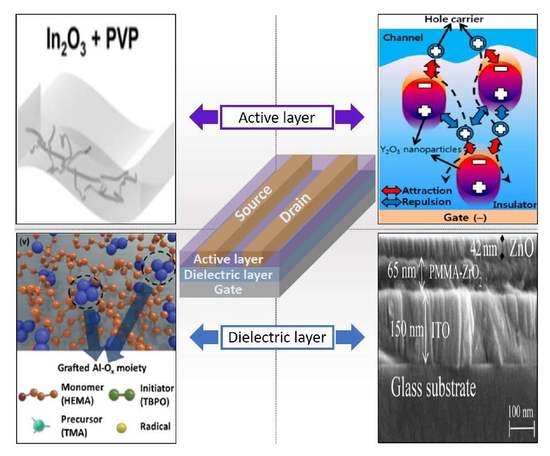
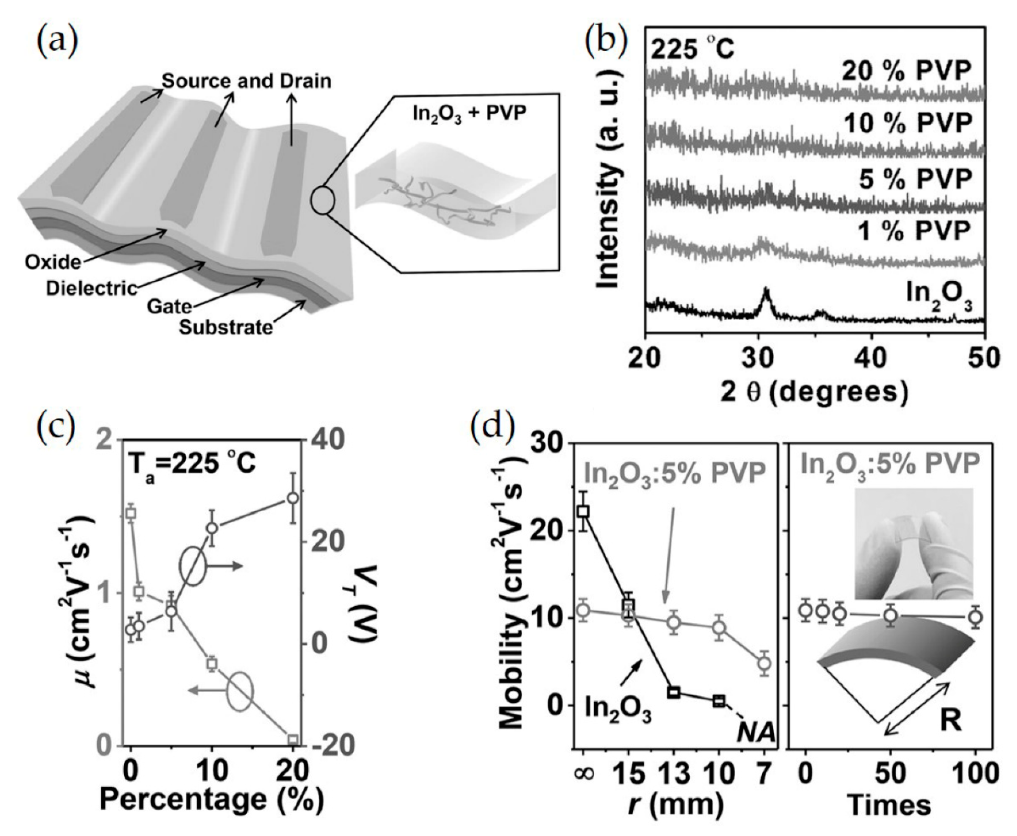
To improve mechanical flexibility of metal oxide (MO) films, polymers such as poly(4-vinylphenol) (PVP), polytetrafluoroethylene (PTFE), and polyethylenimine (PEI) were utilized as doping agents to improve flexibility, as well as to form the amorphous phase of MO [35,87,88,89,90]. For example, Yu et al. developed a new low temperature approach to high-mobility amorphous metal oxide semiconductor films via doping with an insulating polymer, poly(4-vinylphenol) (PVP), to fabricate amorphous MO: polymer blend composites, as depicted in Figure 3a [91]. It should be noted that PVP possesses excellent solubility in the In2O3 precursor solution and their hydroxyl groups favor coordination with the MO lattice. Such an approach effectively prevents crystallization, controls the carrier concentration in the In2O3 channel, and retains conducting pathways for efficient charge transportation. In greater detail, all-amorphous and transparent bottom-gate top-contact thin-film transistors (TFTs) were fabricated via spin-coating of In2O/PVP precursor solutions on AryLite substrates and annealing at 225–250 °C. They exhibited high transparency (< 80%) and low sheet resistance (< F Ω sq−1). In2O3: 5% PVP TFTs exhibited electron mobilities of 11 cm2 V−1 s−1. As the amount of PVP content increases, the In2O3 films become amorphous even with 1 wt % of PVP, as confirmed by grazing incidence X-ray diffraction (GIXRD)(Figure 3b). VT shifts to a positive value and the mobility slightly decreases upon incorporation of PVP, as evidenced in Figure 3c, owing to the carrier concentration modulation from PVP-induced electron traps. The bending/relaxation measurement is to characterize durability of flexible films. A film is bended and relaxed several times with defined radius and then electronic properties are measured. It is worth noting that smaller radius is for more harsh condition; the bending radii that are required for flexible, rollable, and foldable displays are 0r, 10r, and 1r, respectively [92]. The bending tests indicate that the In2O3: 5%PVP hybrid films exhibit only a slight decrease in the mobility from 10.9 to 8.9 cm2 V−1 s−1 as the bending radius decreases to 10 mm, while the pristine In2O3 films, in stark contrast, show dramatic deterioration of the mobility from 22.2 to 0.5 cm2 V−1 s−1 (Figure 3d). Importantly, the value retains up to ca. 90% of their performance even after undergoing repeated mechanical stress (bending/relaxing 100 times).
Polyethylenimine (PEI) is a commercially available polymer capable of efficient n-doping due to the electron-donating nature of the tertiary amine groups (Figure 4a). PEI electron doping has been reported for several organic semiconductors and is widely used in organic photovoltaic cells and transistors to enhance the charge transportation in other organic materials. In this context, Huang et al. fabricated In2O3 / PEI TFT devices via doping of metal oxides with PEI [93]. Doping of In2O3 with PEI effectively prevents crystallization of MOs, controls the carrier concentration in the In2O3 channel, and increases the electron mobility of the In2O3 matrix. In greater detail, a PEI-doped In2O3 blend (i.e., aqueous PEI-In2O3 precursor solutions) was coated on Si substrates with 300 nm SiO2, followed by annealing at 250 °C for 30 min. The addition of PEI successfully inhibits the formation of crystalline structure, which is unfavorable for application in flexible devices as characterized by GIXRD in Figure 4b. The characteristic peaks at 22.1°, 31.1°, 36.0°, and 46.3° ascribed to crystalline In2O3 are strongly suppressed even with a PEI concentration of >1%. Extended X-ray absorption fine structure (EXAFS) measurements correlate the effect of PEI with the TFT mobility. The coordination number (CN) of In-O at the first shell remains intact independent of the PEI doping concentrations, while the second shell CN exhibits the PEI content dependency, decreasing from 6 to 4.05 as the PEI concentration increases (Figure 4c). This indicates that PEI disrupts the formation of lattices, and thus electron conduction pathways. The devices fabricated with polymer concentration of 1–1.5% resulted in excellent mobility up to 9 cm2 V−1 s−1 and high on/off ratio of 107, while that fabricated with pure In2O3 only exhibited a maximum value of 9 cm2 V−1 s−1 (Figure 4d). It is because the electron donating nature of PEI results in doping of In2O3 and matrix film microstructure tuning, yielding high mobilities alongside optimal off-current (Ioff) and threshold voltage (Vth).
The same research group also investigated the charge transportation and film microstructure evolution of PEI-doped amorphous Zn- and/or Ga-incorporated In2O3 thin films [94]. PEI doping generality was expanded from binary In2O3 to ternary (e.g., In + Zn in IZO, In + Ga in IGO) and quaternary (e.g., In + Zn + Ga in IGZO) metal oxide matrices. PEI-metal oxide precursor solutions on Si wafers with 300 nm wide thermally grown SiO2 layers were first spin-casted and then thermally annealed at 300 °C. In this study, the effect of PEI doping concentration and the addition of secondary ions (Ga and Zn) to In2O3 on the device performance was investigated. It was found that the incorporation of Zn and PEI in In2O3 and IGO led to an increase in the surface roughness, thereby degrading the charge transport properties. The crystallinity of In2O3 or IG(Z)O was effectively suppressed and it was observed to monotonically decrease as the PEI concentration was increased. The layer formed adjacent to the dielectric improves the efficiency of charge transportation in a channel when PEI content is low because of trap prefilling. When PEI concentration exceeds a certain threshold, the mobility of the resulting devices begins to decrease due to the disruptions in film continuity and increased trap sites.
Na et al. demonstrated flexible IGZO:PTFE TFTs with improved stability and endurability against water exposure using the facile method of blending the MO semiconductor with polytetrafluoroethylene (PTFE) via plasma polymerization [95]. In greater detail, the IGZO: PTFE layer was co-sputtered with radio frequency magnetron sputtering processes. The hydrophobic nature of PTFE enhances device performance (μFE exceeding 10 cm2 V−1 s−1) and stability (a Vth shift of 0.68 V after an hour of immersion in water) by preventing the adsorption of water molecules on the back surface of TFTs (Figure 5a). Such an approach also improves the electrical stability of IGZO: PTFE TFTs in positive bias stress (PBS), positive bias temperature stress (PBTS), positive bias illumination stress (PBIS), negative bias stress (NBS), negative bias temperature stress (NBTS), and negative bias illumination stress (NBIS) stability tests. Indeed, Vth of IGZO: PTFE TFT remains steady, with only a shift of 0.68 V, while that of IGZO TFTs exhibits significant negative shifts by 12.17 V, as depicted in Figure 5b,c. The improved mechanical flexibility resulting from the soft nature of PTFE enhances the mechanical durability, as depicted in Figure 5d. Specifically, the IGZO: PTFE TFT can retain its performance with no substantial change in its electrical characteristics (a Vth shift of 0.89 V from 3.95 to 3.06 V) over 10000 bending cycles with a bending radius of 5 mm. In contrast, the IGZO TFTs exhibit a significant Vth shift of 5.45 V, from 3.07 to −2.38 V.
Sun et al. reported a strategy to control the geometry and enhance device performance of inkjet-printed MOTFT arrays via the addition of an insulating polymer to the precursor solution prior to film deposition [96]. To prevent the formation of a non-uniform geometry during inkjet-printing, the polymer additive, polystyrene (PS) was utilized. It was reported that the addition of high viscous polymers is favorable to eliminate coffee ring effects by significantly reducing the solute mobility and thus suppressing outward capillary flow of solute to the edge. In detail, PS, with different molecular weights ranging from 2000 to 2,000,000, was mixed with indium precursors (i.e., indium nitrate hydrate) and then printed on silicon substrates, followed by annealing at 225 °C for 1 h. Interestingly, 202 with an increase in PS MW, the coffee ring effect gradually faded, as measured by optical microscope in Figure 6a. The change in surface morphology by varying PS MW is attributed to the suppressed capillary flow and the Marangoni effect. The relative viscosities of In2O3/PS precursor solutions to those of pristine In2O3 solution are 1.02, 1.17, 1.39, and 1.31 for PS with MW of 2000, 20,000, 200,000, and 2,000,000, respectively. Evidently, the use of PS with MW of 20,000 results in smooth films as the increased viscosity inhibits the capillary flow, thus facilitating the depinning of the contact line. The incorporation of PS results in the improvement of carrier mobility from 4.2 cm2 V−1 s−1 up to 13.7 cm2 V−1 s−1 as PS MW increases from 2000 to 2,000,000, which is about three times that of the pristine In2O3 TFTs (Figure 6b). The trap densities for pristine, PS Mw of 2000, 20,000, 200,000, and 2,000,000 were 2.4 × 10¹², 1.2 × 10¹², 1.1 × 10¹², 1.0 × 10¹², and 1.1 × 1012 cm−2 eV−1, respectively. XPS characterization shows that the incorporation of PS obviously impacts local bonding of MO:PS blends, thereby increasing M-O concentration (Figure 6c). Grazing incidence X-ray diffraction indicates that the addition of PS favors the formation of amorphous phase and enhances the M-O lattice contents, both of which facilitate the carrier transportation.
3.2. Dielectric Layers
MOs have been considered to be a crucial component in thin-film electronic systems due to their outstanding electrical and mechanical properties [97,98,99,100,101,102,103,104]. However, the MOs lack flexibility, which limits their use in flexible electronics [105]. Thus far, most thin high-k inorganic metal oxide dielectrics have been fabricated via conventional vacuum-based techniques including pulsed laser deposition (PLD), atomic layer deposition (ALD), magnetron sputtering, and e-beam evaporation. However, these methods are costly and unsuitable to produce large-area flexible oxide electronics. For example, high-quality gate dielectric SiO2 films are produced via expensive vacuum-based plasma-enhanced chemical vapor deposition (PECVD) at high temperatures above 300 °C. It is worth noting that such high temperatures may cause deformation or warping of flexible substrates. Although high performances have been achieved, flexibility and stability still limit their application in real products such as wearable devices. Moreover, dielectric layers (e.g., SiO2) are vulnerable to mechanical stress notwithstanding their extremely thin width, yielding cracks or delamination under mechanical deformation even at small bending radii. In this context, organic dielectrics have garnered substantial attention in the area of flexible devices owing to their flexibility, mechanical stability, low temperature, easy solution processability, and excellent compatibility with flexible organic substrates, despite their low k value [105,106,107,108,109,110]. Therefore, hybridization of organic and inorganic materials can lead to the improvement in flexibility, dielectric constant, and mechanical toughness of gate dielectric materials [111,112,113,114,115,116,117,118,119]. The transistor parameters critically depend on the interface formed between dielectric and semiconductor layers since the trapped charges strongly impact the electrical behavior. The hybrid gate dielectrics tend to be compatible with either organic or inorganic semiconductors. As the inorganic constituent, high-k inorganic nanoparticles such as ZrO2, Al2O3, Y2O3, Ta2O5, and TiO2 were usually embedded in a polymeric matrix such as poly(methylmethacrylate) (PMMA) and poly(vinylpyrrolidone) [120,121,122]. However, the inorganic nanoparticles tend to agglomerate, increasing the surface roughness of the hybrid layers, resulting in high gate leakage current and low on/off current ratio. In this section, the development of hybrid organic–inorganic composites with low power consumption, low operating voltage, and compatibility with transparent flexible electronics for the use in dielectric layers will be summarized.
Poly(methyl methacrylate) (PMMA) is an important thermoplastic polymer with excellent transparency, a refractive index of n = 1.49, good chemical resistance, thermal stability, mechanical flexibility, low cost, and a lower dielectric constant (2.9) than that of silicon oxide material (3.9) [123,124,125,126]. As a result, PMMA has been mixed with high-k inorganic nanoparticles such as ZrO2, Al2O3, and TiO2 to provide high optical transparency, low weight, mechanical flexibility, and formability [14,127,128]. The low temperature deposition process towards PMMA-ZrO2 nanocomposites as dielectric gate layers has been reported [129]. Intriguingly, to prevent phase separation, inorganic oxides were cross-linked with PMMA and trimethoxy-silyl-propyl-methacrylate (TMSPM) molecules that are chemically compatible with both inorganic and organic phases. In greater detail, TFT devices with a ZnO/PMMA-ZrO2/ITO/glass structure (Figure 7a) were fabricated and their electrical properties, such as threshold voltage, channel mobility, and Ion/Ioff current ratio, were investigated. A hybrid dielectric layer was prepared via a sol−gel reaction among zirconium propoxide (ZP), TMSPM, and methylmethacrylate (MMA) precursors at variable TMSPM molar ratios. The devices fabricated with 0.3 M TMSPM exhibit a mobility of 0.48 cm2/V s, on/off ratio of 106–107, and a threshold voltage of 3.3 V. The leakage current density increases from 10−6 to 10−5 A/cm2 as the amount of TMSPM content increases in the hybrid insulating layer, as illustrated in the current density versus electric field characteristic curves (Figure 7b). Importantly, the threshold voltage of the devices decreases from 3.3 V to 0.9 V with an increase in the TMSPM amount from 0.3 M to 0.75 M, as measured by transfer curves in Figure 7c. This feature is advantageous for low power consumption.
Yttrium oxide (Y2O3) nanoparticles exhibit a wide band gap of 6.0 eV, which is advantageous to the aspects of illumination stability of TFTs [130]. In this context, TFTs were fabricated on polyimide (PI) substrates using cross-linked poly(4-vinylphenol) (c-PVP)/ Y2O3 nanocomposites as gate insulators [131]. The architecture of the flexible devices was Ag/6,13-bis(triisopropylsilylehtynyl)pentacene(TIPS-pentacene)/ c-PVP:Y2O3/c-PVP/PI. In greater detail, the cross-linkable PVP was prepared by dissolving PVP and a cross-linking agent, (methylated poly(melamine-co-formaldehyde), MMF) in propylene glycol methyl ether acetate (PGMEA). TFTs with c-PVP:Y2O3 hybrid dielectric exhibited an on-state drain current of −0.165 μA at a gate voltage of −40 V, which is higher than that of devices with only c-PVP (−0.0462 μA), as depicted in Figure 8a,b. However, as illustrated in Figure 8c,d the c-PVP/Y2O3 composite films exhibited a higher roughness compared to the c-PVP films, leading to a larger interference in hole conduction at the interface between the insulator and the semiconductor. Additionally, c-PVP: Y2O3-based TFTs exhibited a greater number of leakage paths for the gate current compared to c-PVP-based TFTs, possibly owing to several interactions like i) the attraction of hole carriers by the highly polarized Y2O3 nanoparticles, ii) flow along the direction of the gate electric field, and iii) repulsion by the positive side and attraction by other adjacent side of the Y2O3 nanoparticles (Figure 8e–g).
Kim et al. have introduced TiO2-polymer composites via cross-linking reactions of these two constituents with low surface energy which allows vertical growth of organic molecules (e.g., pentacene) [132]. In greater detail, a TiO2 precursor (titanium(IV) butoxide and acetyl acetone) and poly(4-vinylphenol) (PVP) solution (PVP, poly(melamine-co-formaldehyde) methylated/butylated and propylene glycol methyl ether acetate (PGMEA) solvent) mixture were spin-coated on ITO substrates and then annealed at 200 °C for 1 h. Interestingly, poly(melamine-co-formaldehyde) methylated/butylated acts as the cross-linker, which reacts with the hydroxyl group of the PVP and the ligands of the TiO2, forming a dense structure. The resulting device exhibits a charge carrier mobility of 0.105 cm2 V−1 s−1, on/off ratio of 103, and a leakage current of 10−7 A cm−2 at ±5 V due to such a dense structure. Furthermore, this homogeneous TiO2-polymer composite solution is stable in ambient conditions. Bang et al. fabricated bottom-gate ZnO-thin film transistors using PVP/Al2O3 dielectrics and investigated the effects of an organic/inorganic dielectric on device performance [133]. The leakage current of the PVP/Al2O3 dielectric improved by three times over the PVP counterparts. The saturation mobility of PVP/Al2O3 TFTs also improved from 0.05 to 0.8 cm2 V−1 s −1 compared to PVP TFTs.
Despite superior mechanical flexibility, organic materials as gate insulators, such as poly-4-vinylphenol (PVP) and polymethyl methacrylate (PMMA), exhibit very low capacitance compared to inorganic dielectrics. In this context, several approaches to improve the capacitance have been introduced. This includes reducing the thickness of dielectric films and incorporating high-k inorganic nanoparticles. However, the use of ultra-thin organic dielectrics often resulted in structural imperfections, producing current leakage. Kim et al. proposed a novel vapor-phase synthesis method to form an ultrathin, homogeneous, high-k organic−inorganic hybrid dielectric [134]. Hybrid dielectrics are synthesized via initiated chemical vapor deposition (iCVD) in a one-step manner (Figure 9a). This method utilizes 2-hydroxyethyl methacrylate and trimethylaluminum as the monomer and the inorganic precursor, respectively. A uniform and defect-free hybrid dielectric layer with precise thickness below 20 nm and composition can be produced. The hybrid films are formed via following subsequent steps—the injection of vaporized monomers, precursors, and initiators, the thermal decomposition of initiators to form free radicals, the adsorption of monomers and precursors, and free-radical polymerization of monomers. The hybrid dielectric exhibits a high k-value of 7 and a low leakage current density of less than 3 × 10⁻⁷ A/cm2 at 2 MV/cm, even with a thickness of less than 5 nm. The capacitance (Ci) versus electric field and the current density (J) versus electric field characterizations corresponding to varying hybrid film thicknesses were also investigated, as illustrated in Figure 9b. As the thickness decreases, the Ci and J values reach 250 nF/cm2 and 1 × 10⁻⁷ A/cm2, respectively. The n- and p-type OTFTs were fabricated using the hybrid dielectric deposited via the iCVD process and their charge-transfer curves were studied, as depicted in Figure 9c,d. The hybrid dielectric offered a superior interface between the channel and dielectric and thus induced ideal charge-transfer characteristics. Both n- and p-type OFETs with the hybrid dielectric exhibited no apparent hysteresis and a low leakage current density (<3 × 10⁻⁷A/cm2 at 2 MV/cm). Furthermore, the dielectric layer exhibited improved chemical stability without any degradation in its dielectric performance. Interestingly, the hybrid dielectric layer retained its excellent dielectric performance under tensile strains of up to 2.6%.
The effects of the device architecture on indium zinc oxide (IZO) TFTs with poly(4-vinylphenol-co-methylmethacrylate) (PVP-co-PMMA) gate insulators were investigated [135]. The top gate IZO TFTs exhibited the improved μFE, SS, Vth, and good Ion/off ratio of 8.5 cm2 V−1 s−1, 2.0 V per decade, -10.0 V, and 107, respectively, compared to the bottom gate IZO TFTs (μFE, SS, Vth, and Ion/off ratio were 9.0 cm2 V−1 s−1, 5.0 V per decade, −12.5 V, and 2 × 10⁵, respectively). This is attributed to the energetic ion bombardment in the polymer gate dielectric layer during the sputtering process. The device performance can be further improved by doping the hybrid PVP-co-PMMA gate dielectric with ZrO2: the μFE, SS, Vth and Ion/off ratio in this case were 28.4 cm2 V−1 s−1, 0.70 V per decade, −2.0, and 4.0 × 10⁷, respectively.
To improve surface contact with organic molecules and increase dielectric properties, a bilayer structure was introduced. For example, Held et al. fabricated a bilayer hybrid dielectric consisting of a high-k hafnium oxide (HfOx)/thin PMMA layer with a donor-acceptor polymer, poly(2,5-bis(2-octyldodecyl)–3-(5–(thieno[3,2-b]thiophen-2,5-yl)thiophen-2-yl)–6-(thiophen-2,5-yl)pyrrolo[3,4-c]pyrrole-1,4(2H,5H)-dione) (DPPT-TT) or single-walled carbon nanotubes (SWNTs) as the semiconductor [136]. PMMA layers were spin-casted and hafnium oxide layers were deposited via ALD. The resulting FETs exhibited drastically reduced operating voltages. The PMMA/HfOx hybrid dielectric exhibited low-voltage operation, well-balanced charge carrier transport, low trap densities, and excellent bias stress stability as PMMA ensures a low density of trap states at the semiconductor dielectric interface and HfOx layers provide high capacitance (Figure 10a). Moreover, the effects of a hybrid dielectric layer for SWNT-FETs were investigated. The SWNT-FETs with only HfOx dielectric layer exhibit strong threshold shift and hysteresis, as observed in the transfer characteristics (Figure 10b). In contrast, ambipolar transfer characteristics without hysteresis was observed in SWNT-FETs with the hybrid dielectric (Figure 10c). According to bias stress tests, SWNT-FETs with hybrid dielectric exhibit constant on-currents without any noticeable degradation over 10 h, while SWNT/HfOx FETs suffer an on-current decay of an order of magnitude recorded in Figure 10d.
High performance low-voltage pentacene-based organic TFTs with pentacene/PMMA/Al2O3/ITO architecture were fabricated and their electronic characteristics were investigated [137]. In this study, a high-k metal oxide dielectric, Al2O3, was used due to its excellent dielectric constant (k = 7.0~9.0) and large bandgap (Eg = 8.45~9.9 eV). PMMA renders improved interfacial properties between Al2O3 and organic pentacene. The OFETs with only an Al2O3 layer exhibited a field-effect mobility of 0.65 cm2/Vs, a threshold voltage of −0.6 V,Ion/Ioff ratio of 4 × 10³, and a sub-threshold swing of 0.45 V/dec, at operating voltages as low as −4 V. After being modified by PMMA, the mobility increased from 0.65 to 0.84 cm2/Vs.
Poly(α-methylstyrene) (PαMS) was also applied on top of zirconium oxide (ZrO2) layers to improve the quality of the interfaces between ZrO2 and organic semiconductors [138]. In greater detail, a ZrO2 film was synthesized on Si via a chemical solution process and annealed at temperatures between 400 and 700 °C. PαMS or HMDS layers were then spin-casted and made to undergo vacuum evaporation with pentacene. It was found that the surface modifications greatly affect the electrical performance of the ZrO2 OTFTs. The surface energy deceased after surface modification and the calculated values are 43.9, 37.8, and 35.5 mJ/m2 for bare-ZrO2, HMDS-ZrO2, and PαMS-ZrO2, respectively, as depicted in Figure 11a–c. The PαMS modified devices exhibited a higher carrier mobility and on/off ratio than those fabricated with bare ZrO2 and HMDS-coated ZrO2 because the PαMS/ZrO2 layers provide a low surface energy and thus promote the growth of large pentacene crystals. In particular, the carrier mobility of the devices with PαMS-modified ZrO2 were observed to increase remarkably from 0.08 to 0.51 cm2/Vs, whereas the carrier mobilities of the devices with bare ZrO2 and HMDS-modified ZrO2 remained at values of ~0.06 and ~0.11 cm2/Vs, respectively, while the dielectric constant of ZrO2 was increased from 12.17 to 19.70 (Figure 11d). Furthermore, PαMS/ZrO2 OTFTs fabricated on flexible polyethyleneterephthalate (PET) substrate were demonstrated, as depicted in Figure 11e,f. The flexible OTFTs exhibited typical IDS-VGS curves of the ZrO2-OFET, exhibiting a ~105 on/off-current ratio between +1 V and −5 V of VGS (Figure 11g).
Ha et al. have reported on low-voltage OTFTs employing solution-processed hybrid bilayer gate dielectric of high-k ZrO2 and low-k amorphous fluoropolymer, CYTOP [139]. The thin hydrophobic CYTOP layer repels aqueous molecules from an organic active layer. Therefore, such device architecture improves electronic characteristics including field effect mobility (from 0.18 to 0.28 cm2/Vs), threshold voltage (Vth, from 0.4 to -0.1 V), and sub-threshold (S.S., 0.57 to 0.28 V/decade) compared to only high-k ZrO2 devices. The reduction in defect-states at the interface suppresses photo-induced hysteresis and enhances the stability of device performance against electric bias-stress.
4. Summary and Outlook
In summary, we first give an overview of the development in polymer/metal oxide nanocomposites for applications in flexible charge transport channels and dielectrics. Recently, metal oxides (MOs) have been fabricated via vacuum-based techniques including pulsed laser deposition (PLD), atomic layer deposition (ALD), magnetron sputtering, and e-beam evaporation, for use in flexible and transparent charge transport channels. Despite their ultra-thin width, only inorganic MO films are vulnerable to repeated mechanical deformation. As a response to low mechanical durability and flexibility, hybrid polymer/MO nanocomposites have been introduced. Hybridization with soft organic materials have proven to be an effective strategy that not only offers mechanical flexibility but also enables solution-based fabrication.
Organic dielectrics have garnered substantial attention owing to their flexibility, mechanical stability, solution processability, and excellent compatibility with flexible organic substrates. However, the low k values of such materials prohibit their application in practical electronic devices. Thereby, high-k inorganic MOs have been employed as fillers. Considering that most of the flexible substrates and semiconductors are organic materials, hybrid gate dielectrics tend to provide good compatibility with organic substrates and semiconductors.
Despite significant advances in flexible electronics by using polymers, many challenges remain to be surmounted, including poor mechanical durability, low charge-carrier mobility, and low dielectric constants. However, we believe that hybrid nanocomposites will reach their full potential in flexible electronics in the near future, as various methods to overcome their weaknesses are being continuously explored.
Author Contributions
Author Contributions: Literature search and review, J.W.J., H.S.H., D.C., J.J., and M.C.; Writing—original draft preparation, J.W.J., H.S.H., B.C.M., J.J., and M.C.; Writing—review and editing, H.S.H., B.C.M., J.J., and M.C. All authors have read and agreed to the published version of the manuscript.
Funding
This work was supported by the National Research Foundation of Korea with a grant funded by the Korean government (Ministry of Science, ICT & Future Planning, MSIP) (NRF-2017R1C1B5017856 and NRF-2017R1C1B1004605). This study was also supported by Basic Science Research Program through the National Research Foundation of Korea funded by the Ministry of Education (NRF-2019R1I1A1A01061532).
Conflicts of Interest
The authors declare no conflict of interest.
References
- Ju, S.; Facchetti, A.; Xuan, Y.; Liu, J.; Ishikawa, F.; Ye, P.; Zhou, C.; Marks, T.J.; Janes, D.B. Fabrication of Fully Transparent Nanowire Transistors for Transparent and Flexible Electronics. Nat. Nanotechnol. 2007, 2, 378. [Google Scholar] [CrossRef] [Green Version]
- Park, S.; Vosguerichian, M.; Bao, Z. A Review of Fabrication and Applications of Carbon Nanotube Film-Based Flexible Electronics. Nanoscale 2013, 5, 1727–1752. [Google Scholar] [CrossRef] [PubMed]
- McCoul, D.; Hu, W.; Gao, M.; Mehta, V.; Pei, Q. Recent Advances in Stretchable and Transparent Electronic Materials. Adv. Electron. Mater. 2016, 2, 1500407. [Google Scholar] [CrossRef]
- Khang, D.-Y.; Jiang, H.; Huang, Y.; Rogers, J.A. A Stretchable Form of Single-Crystal Silicon for High-Performance Electronics on Rubber Substrates. Science 2006, 311, 208–212. [Google Scholar] [CrossRef] [PubMed] [Green Version]
- Kim, D.H.; Kim, Y.S.; Wu, J.; Liu, Z.; Song, J.; Kim, H.S.; Huang, Y.Y.; Hwang, K.C.; Rogers, J.A. Ultrathin Silicon Circuits with Strain-Isolation Layers and Mesh Layouts for High-Performance Electronics on Fabric, Vinyl, Leather, and Paper. Adv. Mater. 2009, 21, 3703–3707. [Google Scholar] [CrossRef]
- Faraji, S.; Danesh, E.; Tate, D.J.; Turner, M.L.; Majewski, L.A. Cyanoethyl Cellulose-Based Nanocomposite Dielectric for Low-Voltage, Solution-Processed Organic Field-Effect Transistors (OFETs). J. Phys. D 2016, 49, 185102. [Google Scholar] [CrossRef] [Green Version]
- Schroeder, R.; Majewski, L.A.; Grell, M. High-Performance Organic Transistors Using Solution-Processed Nanoparticle-Filled High-k Polymer Gate Insulators. Adv. Mater. 2005, 17, 1535–1539. [Google Scholar] [CrossRef]
- Cai, W.; Wilson, J.; Zhang, J.; Park, S.; Majewski, L.; Song, A. Low-Voltage, Flexible InGaZnO Thin-Film Transistors Gated with Solution-Processed, Ultra-Thin Alx Oy. IEEE Electron Device Lett. 2018, 40, 36–39. [Google Scholar]
- Majewski, L.A.; Schroeder, R.; Grell, M. One Volt Organic Transistor. Adv. Mater. 2005, 17, 192–196. [Google Scholar] [CrossRef]
- Cai, W.; Park, S.; Zhang, J.; Wilson, J.; Li, Y.; Xin, Q.; Majewski, L.; Song, A. One-Volt IGZO Thin-Film Transistors With Ultra-Thin, Solution-Processed AlxOy Gate Dielectric. IEEE Electron Device Lett. 2018, 39, 375–378. [Google Scholar] [CrossRef]
- Cai, W.; Wilson, J.; Zhang, J.; Brownless, J.; Zhang, X.; Majewski, L.A.; Song, A. Significant Performance Enhancement of Very-Thin InGaZnO Thin-Film Transistors by a Self-Assembled Monolayer Treatment. ACS Appl. Electron. Mater. 2020, 2, 301–308. [Google Scholar] [CrossRef] [Green Version]
- Lu, J.; Wong, C.P. Recent Advances in High-k Nanocomposite Materials for Embedded Capacitor Applications. IEEE. Trans. Dielectr. Electr. Insul. 2008, 15, 1322–1328. [Google Scholar]
- Liu, J.; Buchholz, D.B.; Hennek, J.W.; Chang, R.P.; Facchetti, A.; Marks, T.J. All-Amorphous-Oxide Transparent, Flexible Thin-Film Transistors. Efficacy of Bilayer Gate Dielectrics. J. Am. Chem. Soc. 2010, 132, 11934–11942. [Google Scholar] [CrossRef] [PubMed]
- Lee, J.-W.; Ju, B.-K.; Jang, J.; Yoon, Y.-S.; Kim, J.-K. High Mobility Organic Transistor Patterned by the Shadow-Mask with All Structure on a Plastic Substrate. J. Mater. Sci. 2007, 42, 1026–1030. [Google Scholar] [CrossRef]
- Lee, I.-Y.; Park, H.-Y.; Park, J.-H.; Yoo, G.; Lim, M.-H.; Park, J.; Rathi, S.; Jung, W.-S.; Kim, J.; Kim, S.-W. Poly-4-vinylphenol and Poly (melamine-co-formaldehyde)-Based Graphene Passivation Method for Flexible, Wearable and Transparent Electronics. Nanoscale 2014, 6, 3830–3836. [Google Scholar] [CrossRef] [PubMed]
- Trung, T.Q.; Tien, N.T.; Kim, D.; Jang, M.; Yoon, O.J.; Lee, N.E. A Flexible Reduced Graphene Oxide Field-Effect Transistor for Ultrasensitive Strain Sensing. Adv. Funct. Mater. 2014, 24, 117–124. [Google Scholar] [CrossRef]
- Schattka, J.H.; Shchukin, D.G.; Jia, J.; Antonietti, M.; Caruso, R.A. Photocatalytic Activities of Porous Titania and Titania/Zirconia Structures Formed by Using a Polymer Gel Templating Technique. Chem. Mater. 2002, 14, 5103–5108. [Google Scholar] [CrossRef]
- Kim, J.H.; Hwang, B.-U.; Kim, D.-I.; Kim, J.S.; Seol, Y.G.; Kim, T.W.; Lee, N.-E. Nanocomposites of Polyimide and Mixed Oxide Nanoparticles for High Performance Nanohybrid Gate Dielectrics in Flexible Thin Film Transistors. Electron. Mater. Lett. 2017, 13, 214–221. [Google Scholar] [CrossRef]
- Madusanka, N.; Shivareddy, S.G.; Hiralal, P.; Eddleston, M.D.; Choi, Y.; Oliver, R.A.; Amaratunga, G.A.J. Nanocomposites of TiO2/Cyanoethylated Cellulose with Ultra High Dielectric Constants. Nanotechnology 2016, 27, 195402. [Google Scholar] [CrossRef] [Green Version]
- Beaulieu, M.R.; Baral, J.K.; Hendricks, N.R.; Tang, Y.; Briseño, A.L.; Watkins, J.J. Solution Processable High Dielectric Constant Nanocomposites Based on ZrO2 Nanoparticles for Flexible Organic Transistors. ACS Appl. Mater. Interfaces 2013, 5, 13096–13103. [Google Scholar] [CrossRef]
- Yang, W.; Song, K.; Jung, Y.; Jeong, S.; Moon, J. Solution-Deposited Zr-doped AlOx Gate Dielectrics Enabling High-Performance Flexible Transparent Thin Film Transistors. J. Mater. Chem. C 2013, 1, 4275–4282. [Google Scholar] [CrossRef]
- Min, Y.-S.; Cho, Y.J.; Hwang, C.S. Atomic Layer Deposition of Al2O3 Thin Films from a 1-methoxy-2-methyl-2-propoxide Complex of Aluminum and Water. Chem. Mater. 2005, 17, 626–631. [Google Scholar] [CrossRef]
- Jeong, S.; Ha, Y.G.; Moon, J.; Facchetti, A.; Marks, T.J. Role of Gallium Doping in Dramatically Lowering Amorphous-Oxide Processing Temperatures for Solution-Derived Indium Zinc Oxide Thin-Film Transistors. Adv. Mater. 2010, 22, 1346–1350. [Google Scholar] [CrossRef] [PubMed]
- Hennek, J.W.; Smith, J.; Yan, A.; Kim, M.-G.; Zhao, W.; Dravid, V.P.; Facchetti, A.; Marks, T.J. Oxygen “getter” Effects on Microstructure and Carrier Transport in Low Temperature Combustion-Processed a-InXZnO (X = Ga, Sc, Y, La) Transistors. J. Am. Chem. Soc. 2013, 135, 10729–10741. [Google Scholar] [CrossRef] [PubMed]
- Banger, K.K.; Peterson, R.L.; Mori, K.; Yamashita, Y.; Leedham, T.; Sirringhaus, H. High Performance, Low Temperature Solution-Processed Barium and Strontium Doped Oxide Thin Film Transistors. Chem. Mater. 2014, 26, 1195–1203. [Google Scholar] [CrossRef] [PubMed]
- Jo, J.W.; Kim, J.; Kim, K.T.; Kang, J.G.; Kim, M.G.; Kim, K.H.; Ko, H.; Kim, Y.H.; Park, S.K. Highly Stable and Imperceptible Electronics Utilizing Photoactivated Heterogeneous Sol-Gel Metal–Oxide Dielectrics and Semiconductors. Adv. Mater. 2015, 27, 1182–1188. [Google Scholar] [CrossRef]
- Khanal, R.; Buchholz, D.B.; Chang, R.P.; Medvedeva, J.E. Composition-Dependent Structural and Transport Properties of Amorphous Transparent Conducting Oxides. Phys. Rev. B 2015, 91, 205203. [Google Scholar] [CrossRef] [Green Version]
- Nadaud, N.; Lequeux, N.; Nanot, M.; Jove, J.; Roisnel, T. Structural Studies of Tin-Doped Indium Oxide (ITO) and In4Sn3O12. J. Solid State Chem. 1998, 135, 140–148. [Google Scholar] [CrossRef] [Green Version]
- Jin, S.H.; Kang, S.-K.; Cho, I.-T.; Han, S.Y.; Chung, H.U.; Lee, D.J.; Shin, J.; Baek, G.W.; Kim, T.-I.; Lee, J.-H. Water-Soluble Thin Film Transistors and Circuits Based on Amorphous Indium–Gallium–Zinc Oxide. ACS Appl. Mater. Interfaces 2015, 7, 8268–8274. [Google Scholar] [CrossRef]
- Lim, S.H.; Kim, J.; Lee, S.-G.; Kim, Y.S. Water-Soluble Polymer Dielectric with Potential for High Performance Organic Thin-Film Transistors. Chem. Commun. 2010, 46, 3961–3963. [Google Scholar] [CrossRef]
- Byun, H.S.; Xu, Y.-X.; Song, C.K. Fabrication of High Performance Pentacene Thin Film Transistors Using Poly (4-vinylphenol) as the Gate Insulator on Polyethyleneterephthalate Substrates. Thin Solid Films 2005, 493, 278–281. [Google Scholar] [CrossRef]
- Kim, J.-M.; Lee, J.-W.; Kim, J.-K.; Ju, B.-K.; Kim, J.-S.; Lee, Y.-H.; Oh, M.-H. An Organic Thin-Film Transistor of High Mobility by Dielectric Surface Modification with Organic Molecule. Appl. Phys. Lett. 2004, 85, 6368–6370. [Google Scholar] [CrossRef] [Green Version]
- Wei, Q.; You, E.; Hendricks, N.R.; Briseno, A.L.; Watkins, J.J. Flexible Low-Voltage Polymer Thin-Film Transistors Using Supercritical CO2-Deposited ZrO2 Dielectrics. ACS Appl. Mater. Interfaces 2012, 4, 2322–2324. [Google Scholar] [CrossRef] [PubMed]
- De Angelis, F.; Cipolloni, S.; Mariucci, L.; Fortunato, G. High-Field-Effect-Mobility Pentacene Thin-Film Transistors with Polymethylmetacrylate Buffer Layer. Appl. Phys. Lett. 2005, 86, 203505. [Google Scholar] [CrossRef]
- Kato, T.; Suzuki, T.; Amamiya, T.; Irie, T.; Komiyama, M.; Yui, H. Effects of Macromolecules on the Crystallization of CaCO3 the Formation of Organic/Inorganic Composites. Supramol. Sci. 1998, 5, 411–415. [Google Scholar] [CrossRef]
- Zukas, B.G.; Gupta, N.R. Interphase Synthesis of Zinc Oxide Nanoparticles in a Droplet Flow Reactor. Ind. Eng. Chem. Res. 2017, 56, 7184–7191. [Google Scholar] [CrossRef]
- Ali, G.; Park, Y.J.; Kim, J.W.; Cho, S.O. A Green, General, and Ultrafast Route for the Synthesis of Diverse Metal Oxide Nanoparticles with Controllable Sizes and Enhanced Catalytic Activity. ACS Appl. Nano Mater. 2018, 1, 6112–6122. [Google Scholar] [CrossRef]
- Cao, H.; Zhou, X.; Zheng, C.; Liu, Z. Two-Dimensional Porous Micro/Nano Metal Oxides Templated by Graphene Oxide. ACS Appl. Mater. Interfaces 2015, 7, 11984–11990. [Google Scholar] [CrossRef]
- Niederberger, M. Nonaqueous Sol–Gel Routes to Metal Oxide Nanoparticles. Acc. Chem. Res. 2007, 40, 793–800. [Google Scholar] [CrossRef] [Green Version]
- Yu, J.; Yu, X. Hydrothermal Synthesis and Photocatalytic Activity of Zinc Oxide Hollow Spheres. Environ. Sci. Technol. 2008, 42, 4902–4907. [Google Scholar] [CrossRef]
- Ba, J.; Polleux, J.; Antonietti, M.; Niederberger, M. Non-Aqueous Synthesis of Tin Oxide Nanocrystals and Their Assembly into Ordered Porous Mesostructures. Adv. Mater. 2005, 17, 2509–2512. [Google Scholar] [CrossRef]
- Bilecka, I.; Djerdj, I.; Niederberger, M. One-Minute Synthesis of Crystalline Binary and Ternary Metal Oxide Nanoparticles. Chem. Commun. 2008, 886–888. [Google Scholar] [CrossRef] [PubMed]
- Ding, Z.; Hu, X.; Yue, P.L.; Lu, G.Q.; Greenfield, P.F. Synthesis of Anatase TiO2 Supported on Porous Solids by Chemical Vapor Deposition. Catal. Today 2001, 68, 173–182. [Google Scholar] [CrossRef]
- Wang, Y.; Lei, Y.; Li, J.; Gu, L.; Yuan, H.; Xiao, D. Synthesis of 3D-Nanonet Hollow Structured Co3O4 for High Capacity Supercapacitor. ACS Appl. Mater. Interfaces 2014, 6, 6739–6747. [Google Scholar] [CrossRef] [PubMed]
- Gawande, M.B.; Branco, P.S.; Parghi, K.; Shrikhande, J.J.; Pandey, R.K.; Ghumman, C.A.A.; Bundaleski, N.; Teodoro, O.M.N.D.; Jayaram, R.V. Synthesis and Characterization of Versatile MgO–ZrO2 Mixed Metal Oxide Nanoparticles and Their Applications. Catal. Sci. Technol. 2011, 1, 1653–1664. [Google Scholar] [CrossRef]
- Sharma, R.K.; Ghose, R. Synthesis of Nanocrystalline CuO–ZnO Mixed Metal Oxide Powder by a Homogeneous Precipitation Method. Ceram. Int. 2014, 40, 10919–10926. [Google Scholar] [CrossRef]
- Li, J.; Liu, X.; Cui, J.; Sun, J. Hydrothermal Synthesis of Self-Assembled Hierarchical Tungsten Oxides Hollow Spheres and Their Gas Sensing Properties. ACS Appl. Mater. Interfaces 2015, 7, 10108–10114. [Google Scholar] [CrossRef]
- Van Tong, P.; Hoa, N.D.; Van Duy, N.; Le, D.T.T.; Van Hieu, N. Enhancement of Gas-Sensing Characteristics of Hydrothermally Synthesized WO3 Nanorods by Surface Decoration with Pd Nanoparticles. Sens. Actuators B Chem. 2016, 223, 453–460. [Google Scholar] [CrossRef]
- Yeo, J.; Hong, S.; Kim, G.; Lee, H.; Suh, Y.D.; Park, I.; Grigoropoulos, C.P.; Ko, S.H. Laser-Induced Hydrothermal Growth of Heterogeneous Metal-Oxide Nanowire on Flexible Substrate by Laser Absorption Layer Design. ACS Nano 2015, 9, 6059–6068. [Google Scholar] [CrossRef]
- Wang, J.; Yang, P.; Wei, X. High-Performance, Room-Temperature, and No-Humidity-Impact Ammonia Sensor Based on Heterogeneous Nickel Oxide and Zinc Oxide Nanocrystals. ACS Appl. Mater. Interfaces 2015, 7, 3816–3824. [Google Scholar] [CrossRef]
- Lu, B.; Bai, J.; Bo, X.; Zhu, L.; Guo, L. A Simple Hydrothermal Synthesis of Nickel Hydroxide–Ordered Mesoporous Carbons Nanocomposites and Its Electrocatalytic Application. Electrochim. Acta 2010, 55, 8724–8730. [Google Scholar] [CrossRef]
- Liu, Q.; Qin, M.C.; Ke, W.J.; Zheng, X.L.; Chen, Z.; Qin, P.L.; Xiong, L.B.; Lei, H.W.; Wan, J.W.; Wen, J. Enhanced Stability of Perovskite Solar Cells with Low-Temperature Hydrothermally Grown SnO2 Electron Transport Layers. Adv. Funct. Mater. 2016, 26, 6069–6075. [Google Scholar] [CrossRef]
- Ji, H.; Miao, X.; Wang, L.; Qian, B.; Yang, G. Microwave-Assisted Hydrothermal Synthesis of Sphere-like C/CuO and CuO Nanocrystals and Improved Performance as Anode Materials for Lithium-Ion Batteries. Powder Technol. 2013, 241, 43–48. [Google Scholar] [CrossRef]
- Yayapao, O.; Thongtem, T.; Phuruangrat, A.; Thongtem, S. CTAB-Assisted Hydrothermal Synthesis of Tungsten Oxide Microflowers. J. Alloys Compd. 2011, 509, 2294–2299. [Google Scholar] [CrossRef]
- Zhao, R.; Wang, L.; Chai, Z.-F.; Shi, W.-Q. Synthesis of ThO2 Nanostructures through a Hydrothermal Approach: Influence of Hexamethylenetetramine (HMTA) and Sodium Dodecyl Sulfate (SDS). RSC Adv. 2014, 4, 52209–52214. [Google Scholar] [CrossRef]
- Xiao, W.; Wang, Z.; Guo, H.; Zhang, Y.; Zhang, Q.; Gan, L. A Facile PVP-Assisted Hydrothermal Fabrication of Fe2O3/Graphene Composite as High Performance Anode Material for Lithium Ion Batteries. J. Alloys Compd. 2013, 560, 208–214. [Google Scholar] [CrossRef]
- Vishwas, M.; Narasimha Rao, K.; Arjuna Gowda, K.V.; Chakradhar, R.P.S. Influence of Sn Doping on Structural, Optical and Electrical Properties of ZnO Thin Films Prepared by Cost Effective Sol–Gel Process. Spectrochim. Acta A 2012, 95, 423–426. [Google Scholar] [CrossRef]
- Li, X.; Liu, P.; Mao, Y.; Xing, M.; Zhang, J. Preparation of Homogeneous Nitrogen-Doped Mesoporous TiO2 Spheres with Enhanced Visible-Light Photocatalysis. Appl. Catal. B Environ. 2015, 164, 352–359. [Google Scholar] [CrossRef]
- Soo, M.T.; Prastomo, N.; Matsuda, A.; Kawamura, G.; Muto, H.; Noor, A.F.M.; Lockman, Z.; Cheong, K.Y. Elaboration and Characterization of Sol–Gel Derived ZrO2 Thin Films Treated with Hot Water. Appl. Surf. Sci. 2012, 258, 5250–5258. [Google Scholar] [CrossRef]
- Niederberger, M.; Garnweitner, G.; Buha, J.; Polleux, J.; Ba, J.; Pinna, N. Nonaqueous Synthesis of Metal Oxide Nanoparticles:Review and Indium Oxide as Case Study for the Dependence of Particle Morphology on Precursors and Solvents. J. Sol-Gel Sci. Technol. 2006, 40, 259–266. [Google Scholar] [CrossRef]
- Athar, T.; Hakeem, A.; Ahmed, W. Synthesis of MgO Nanopowder via Non Aqueous Sol–gel Method. Adv. Sci. Lett. 2012, 7, 27–29. [Google Scholar] [CrossRef]
- Masthoff, I.C.; Kraken, M.; Menzel, D.; Litterst, F.J.; Garnweitner, G. Study of the Growth of Hydrophilic Iron Oxide Nanoparticles Obtained via the Non-Aqueous Sol–Gel Method. J. Sol-Gel Sci. Technol. 2016, 77, 553–564. [Google Scholar] [CrossRef]
- Singh, I.; Kumar, R.; Birajdar, B.I. Zirconium Doped TiO2 Nano-Powder via Halide Free Non-Aqueous Solvent Controlled Sol–gel Route. J. Environ. Chem. Eng. 2017, 5, 2955–2963. [Google Scholar] [CrossRef]
- Niederberger, M.; Bartl, M.H.; Stucky, G.D. Benzyl Alcohol and Transition Metal Chlorides as a Versatile Reaction System for the Nonaqueous and Low-Temperature Synthesis of Crystalline Nano-Objects with Controlled Dimensionality. J. Am. Chem. Soc. 2002, 124, 13642–13643. [Google Scholar] [CrossRef] [PubMed]
- Mirzaei, A.; Neri, G. Microwave-Assisted Synthesis of Metal Oxide Nanostructures for Gas Sensing Application: A Review. Sens. Actuators B Chem. 2016, 237, 749–775. [Google Scholar] [CrossRef]
- Xi, G.; He, Y.; Zhang, Q.; Xiao, H.; Wang, X.; Wang, C. Synthesis of Crystalline Microporous SnO2 via a Surfactant-Assisted Microwave Heating Method: A General and Rapid Method for the Synthesis of Metal Oxide Nanostructures. J. Phys. Chem. C 2008, 112, 11645–11649. [Google Scholar] [CrossRef]
- Vijayakumar, S.; Nagamuthu, S.; Muralidharan, G. Supercapacitor Studies on NiO Nanoflakes Synthesized Through a Microwave Route. ACS Appl. Mater. Interfaces 2013, 5, 2188–2196. [Google Scholar] [CrossRef]
- Mondal, A.K.; Su, D.; Chen, S.; Kretschmer, K.; Xie, X.; Ahn, H.-J.; Wang, G. A Microwave Synthesis of Mesoporous NiCo2O4 Nanosheets as Electrode Materials for Lithium-Ion Batteries and Supercapacitors. ChemPhysChem 2015, 16, 169–175. [Google Scholar] [CrossRef]
- Ede, S.R.; Anantharaj, S.; Subramanian, B.; Rathishkumar, A.; Kundu, S. Microwave-Assisted Template-Free Synthesis of Ni3(BO3)2(NOB) Hierarchical Nanoflowers for Electrocatalytic Oxygen Evolution. Energy Fuels 2018, 32, 6224–6233. [Google Scholar] [CrossRef]
- Bilecka, I.; Niederberger, M. Microwave Chemistry for Inorganic Nanomaterials Synthesis. Nanoscale 2010, 2, 1358–1374. [Google Scholar] [CrossRef]
- Nomura, K.; Ohta, H.; Takagi, A.; Kamiya, T.; Hirano, M.; Hosono, H. Room-Temperature Fabrication of Transparent Flexible Thin-Film Transistors Using Amorphous Oxide Semiconductors. Nature 2004, 432, 488–492. [Google Scholar] [CrossRef] [PubMed]
- Buchholz, D.B.; Ma, Q.; Alducin, D.; Ponce, A.; Jose-Yacaman, M.; Khanal, R.; Medvedeva, J.E.; Chang, R.P.H. The Structure and Properties of Amorphous Indium Oxide. Chem. Mater. 2014, 26, 5401–5411. [Google Scholar] [CrossRef] [PubMed] [Green Version]
- Thomas, S.R.; Pattanasattayavong, P.; Anthopoulos, T.D. Solution-Processable Metal Oxide Semiconductors for Thin-Film Transistor Applications. Chem. Soc. Rev. 2013, 42, 6910–6923. [Google Scholar] [CrossRef] [PubMed]
- Xu, H.; Luo, D.; Li, M.; Xu, M.; Zou, J.; Tao, H.; Lan, L.; Wang, L.; Peng, J.; Cao, Y. A Flexible AMOLED Display on the PEN Substrate Driven by Oxide Thin-Film Transistors Using Anodized Aluminium Oxide as Dielectric. J. Mater. Chem. C 2014, 2, 1255–1259. [Google Scholar] [CrossRef]
- Cairns, D.R.; Witte, R.P.; Sparacin, D.K.; Sachsman, S.M.; Paine, D.C.; Crawford, G.P.; Newton, R.R. Strain-Dependent Electrical Resistance of Tin-Doped Indium Oxide on Polymer Substrates. Appl. Phys. Lett. 2000, 76, 1425–1427. [Google Scholar] [CrossRef]
- Peng, C.; Jia, Z.; Bianculli, D.; Li, T.; Lou, J. In Situ Electro-Mechanical Experiments and Mechanics Modeling of Tensile Cracking in Indium Tin Oxide Thin Films on Polyimide Substrates. J. Appl. Phys. 2011, 109, 103530. [Google Scholar] [CrossRef] [Green Version]
- Xing, G.Z.; Yi, J.B.; Yan, F.; Wu, T.; Li, S. Positive Magnetoresistance in Ferromagnetic Nd-Doped In2O3 Thin Films Grown by Pulse Laser Deposition. Appl. Phys. Lett. 2014, 104, 202411. [Google Scholar] [CrossRef] [Green Version]
- Imai, H.; Tominaga, A.; Hirashima, H.; Toki, M.; Asakuma, N. Ultraviolet-Reduced Reduction and Crystallization of Indium Oxide Films. J. Appl. Phys. 1999, 85, 203–207. [Google Scholar] [CrossRef]
- Kim, J.Y.; Lee, K.; Coates, N.E.; Moses, D.; Nguyen, T.-Q.; Dante, M.; Heeger, A.J. Efficient Tandem Polymer Solar Cells Fabricated by All-Solution Processing. Science 2007, 317, 222–225. [Google Scholar] [CrossRef] [Green Version]
- Ma, W.; Yang, C.; Gong, X.; Lee, K.; Heeger, A.J. Thermally Stable, Efficient Polymer Solar Cells with Nanoscale Control of the Interpenetrating Network Morphology. Adv. Funct. Mater. 2005, 15, 1617–1622. [Google Scholar] [CrossRef]
- Le, T.-H.; Kim, Y.; Yoon, H. Electrical and Electrochemical Properties of Conducting Polymers. Polymers 2017, 9, 150. [Google Scholar] [CrossRef] [PubMed]
- Kong, H.J.; Kim, S.; Le, T.-H.; Kim, Y.; Park, G.; Park, C.S.; Kwon, O.S.; Yoon, H. Nanostructured Mesophase Electrode Materials: Modulating Charge-Storage Behavior by Thermal Treatment. Nanoscale 2017, 9, 17450–17458. [Google Scholar] [CrossRef] [PubMed] [Green Version]
- Beek, W.J.; Slooff, L.H.; Wienk, M.M.; Kroon, J.M.; Janssen, R.A. Hybrid Solar Cells Using a Zinc Oxide Precursor and a Conjugated Polymer. Adv. Funct. Mater. 2005, 15, 1703–1707. [Google Scholar] [CrossRef]
- Chen, C.-T.; Hsu, F.-C.; Kuan, S.-W.; Chen, Y.-F. The Effect of C60 on the ZnO-Nanorod Surface in Organic–Inorganic Hybrid Photovoltaics. Sol. Energy Mater. Sol. Cells 2011, 95, 740–744. [Google Scholar] [CrossRef]
- Benabid, F.; Kharchi, N.; Zouai, F.; Mourad, A.-H.I.; Benachour, D. Impact of Co-Mixing Technique and Surface Modification of ZnO Nanoparticles Using Stearic Acid on Their Dispersion into HDPE to Produce HDPE/ZnO Nanocomposites. Polym. Polym. Compos. 2019, 27, 389–399. [Google Scholar] [CrossRef]
- Vivekchand, S.; Kam, K.C.; Gundiah, G.; Govindaraj, A.; Cheetham, A.; Rao, C. Electrical Properties of Inorganic Nanowire–Polymer Composites. J. Mater. Chem. 2005, 15, 4922–4927. [Google Scholar] [CrossRef]
- Shim, M.; Javey, A.; Shi Kam, N.W.; Dai, H. Polymer Functionalization for Air-Stable n-Type Carbon Nanotube Field-Effect Transistors. J. Am. Chem. Soc. 2001, 123, 11512–11513. [Google Scholar] [CrossRef]
- Du, Y.; Liu, H.; Neal, A.T.; Si, M.; Ye, P.D. Molecular Doping of Multilayer MoS2 Field-Effect Transistors: Reduction in Sheet and Contact Resistances. IEEE Electron Device Lett. 2013, 34, 1328–1330. [Google Scholar] [CrossRef] [Green Version]
- Sun, B.; Hong, W.; Thibau, E.S.; Aziz, H.; Lu, Z.-H.; Li, Y. Polyethylenimine (PEI) As an Effective Dopant To Conveniently Convert Ambipolar and p-Type Polymers into Unipolar n-Type Polymers. ACS Appl. Mater. Interfaces 2015, 7, 18662–18671. [Google Scholar] [CrossRef]
- Fabiano, S.; Braun, S.; Liu, X.; Weverberghs, E.; Gerbaux, P.; Fahlman, M.; Berggren, M.; Crispin, X. Poly(ethylene imine) Impurities Induce n-doping Reaction in Organic (Semi)Conductors. Adv. Mater. 2014, 26, 6000–6006. [Google Scholar] [CrossRef] [Green Version]
- Yu, X.; Zeng, L.; Zhou, N.; Guo, P.; Shi, F.; Buchholz, D.B.; Ma, Q.; Yu, J.; Dravid, V.P.; Chang, R.P.H.; et al. Ultra-Flexible, “Invisible” Thin-Film Transistors Enabled by Amorphous Metal Oxide/Polymer Channel Layer Blends. Adv. Mater. 2015, 27, 2390–2399. [Google Scholar] [CrossRef]
- Jeong, E.G.; Kwon, J.H.; Kang, K.S.; Jeong, S.Y.; Choi, K.C. A Review of Highly Reliable Flexible Encapsulation Technologies towards Rollable and Foldable OLEDs. J. Inf. Disp. 2019, 19–32. [Google Scholar] [CrossRef]
- Huang, W.; Zeng, L.; Yu, X.; Guo, P.; Wang, B.; Ma, Q.; Chang, R.P.H.; Yu, J.; Bedzyk, M.J.; Marks, T.J.; et al. Metal Oxide Transistors via Polyethylenimine Doping of the Channel Layer: Interplay of Doping, Microstructure, and Charge Transport. Adv. Funct. Mater. 2016, 26, 6179–6187. [Google Scholar] [CrossRef]
- Huang, W.; Guo, P.; Zeng, L.; Li, R.; Wang, B.; Wang, G.; Zhang, X.; Chang, R.P.H.; Yu, J.; Bedzyk, M.J.; et al. Metal Composition and Polyethylenimine Doping Capacity Effects on Semiconducting Metal Oxide—Polymer Blend Charge Transport. J. Am. Chem. Soc. 2018, 140, 5457–5473. [Google Scholar] [CrossRef] [PubMed]
- Na, J.W.; Kim, H.J.; Hong, S.; Kim, H.J. Plasma Polymerization Enabled Polymer/Metal–Oxide Hybrid Semiconductors for Wearable Electronics. ACS Appl. Mater. Interfaces 2018, 10, 37207–37215. [Google Scholar] [CrossRef] [PubMed]
- Sun, D.; Chen, C.; Zhang, J.; Wu, X.; Chen, H.; Guo, T. High Performance Inkjet-Printed Metal Oxide Thin Film Transistors via Addition of Insulating Polymer with Proper Molecular Weight. Appl. Phys. Lett. 2018, 112, 012102. [Google Scholar] [CrossRef]
- Ha, Y.-G.; Everaerts, K.; Hersam, M.C.; Marks, T.J. Hybrid Gate Dielectric Materials for Unconventional Electronic Circuitry. Acc. Chem. Res. 2014, 47, 1019–1028. [Google Scholar] [CrossRef]
- Wang, G.; Persson, N.; Chu, P.-H.; Kleinhenz, N.; Fu, B.; Chang, M.; Deb, N.; Mao, Y.; Wang, H.; Grover, M.A.; et al. Microfluidic Crystal Engineering of π-Conjugated Polymers. ACS Nano 2015, 9, 8220–8230. [Google Scholar] [CrossRef]
- Yeon Kwon, J.; Kyeong Jeong, J. Recent Progress in High Performance and Reliable N-type Transition Metal Oxide-Based Thin Film Transistors. Semicond. Sci. Technol. 2015, 30, 024002. [Google Scholar] [CrossRef]
- Wager, J.F.; Yeh, B.; Hoffman, R.L.; Keszler, D.A. An Amorphous Oxide Semiconductor Thin-Film Transistor Route to Oxide Electronics. Curr. Opin. Solid State Mater. Sci. 2014, 18, 53–61. [Google Scholar] [CrossRef] [Green Version]
- Navan, R.R.; Prashanthi, K.; Shojaei Baghini, M.; Ramgopal Rao, V. Solution Processed Photopatternable High-k Nanocomposite Gate Dielectric for Low Voltage Organic Field Effect Transistors. Microelectron. Eng. 2012, 96, 92–95. [Google Scholar] [CrossRef]
- Lim, S.; Lee, K.H.; Kim, H.; Kim, S.H. Optimization of Nanocomposite Gate Insulators for Organic Thin Film Transistors. Org. Electron. 2015, 17, 144–150. [Google Scholar] [CrossRef]
- Hou, X.; Ng, S.C.; Zhang, J.; Chang, J.S. Polymer Nanocomposite Dielectric Based on P(VDF-TrFE)/PMMA/BaTiO3 for TIPs-Pentacene OFETs. Org. Electron. 2015, 17, 247–252. [Google Scholar] [CrossRef]
- Rasul, A.; Zhang, J.; Gamota, D.; Takoudis, C. High K Nanocomposite Dielectric for Printed Organic Electronics Applications. Microelectron. Eng. 2012, 93, 95–99. [Google Scholar] [CrossRef]
- Pecunia, V.; Banger, K.; Sirringhaus, H. High-Performance Solution-Processed Amorphous-Oxide-Semiconductor TFTs with Organic Polymeric Gate Dielectrics. Adv. Electron. Mater. 2015, 1, 1400024. [Google Scholar] [CrossRef] [Green Version]
- Sirringhaus, H. 25th Anniversary Article: Organic Field-Effect Transistors: The Path Beyond Amorphous Silicon. Adv. Mater. 2014, 26, 1319–1335. [Google Scholar] [CrossRef] [Green Version]
- Zhang, L.; Wang, H.; Zhao, Y.; Guo, Y.; Hu, W.; Yu, G.; Liu, Y. Substrate-Free Ultra-Flexible Organic Field-Effect Transistors and Five-Stage Ring Oscillators. Adv. Mater. 2013, 25, 5455–5460. [Google Scholar] [CrossRef]
- Khim, D.; Xu, Y.; Baeg, K.-J.; Kang, M.; Park, W.-T.; Lee, S.-H.; Kim, I.-B.; Kim, J.; Kim, D.-Y.; Liu, C.; et al. Large Enhancement of Carrier Transport in Solution-Processed Field-Effect Transistors by Fluorinated Dielectric Engineering. Adv. Mater. 2016, 28, 518–526. [Google Scholar] [CrossRef]
- Li, J.; Liu, D.; Miao, Q.; Yan, F. The Application of a high-k Polymer in Flexible Low-Voltage Organic Thin-Film Transistors. J. Mater. Chem. 2012, 22, 15998–16004. [Google Scholar] [CrossRef]
- Fukuda, K.; Sekine, T.; Shiwaku, R.; Morimoto, T.; Kumaki, D.; Tokito, S. Free-Standing Organic Transistors and Circuits with Sub-Micron Thicknesses. Sci. Rep. 2016, 6, 27450. [Google Scholar] [CrossRef]
- Yu, X.; Smith, J.; Zhou, N.; Zeng, L.; Guo, P.; Xia, Y.; Alvarez, A.; Aghion, S.; Lin, H.; Yu, J.; et al. Spray-Combustion Synthesis: Efficient Solution Route to High-Performance Oxide Transistors. Proc. Natl. Acad. Sci. USA 2015, 112, 3217–3222. [Google Scholar] [CrossRef] [PubMed] [Green Version]
- Chen, H.; Cao, Y.; Zhang, J.; Zhou, C. Large-Scale Complementary Macroelectronics Using Hybrid Integration of Carbon Nanotubes and IGZO Thin-Film Transistors. Nat. Commun. 2014, 5, 4097. [Google Scholar] [CrossRef] [PubMed]
- Rasul, A.; Zhang, J.; Gamota, D.; Singh, M.; Takoudis, C. Flexible High Capacitance Nanocomposite Gate Insulator for Printed Oorganic Field-Effect Transistors. Thin Solid Films 2010, 518, 7024–7028. [Google Scholar] [CrossRef]
- Yang, F.-Y.; Hsu, M.-Y.; Hwang, G.-W.; Chang, K.-J. High-Performance Poly(3-hexylthiophene) Top-Gate Transistors Incorporating TiO2 Nanocomposite Dielectrics. Org. Electron. 2010, 11, 81–88. [Google Scholar] [CrossRef]
- Park, J.; Lee, J.W.; Kim, D.W.; Park, B.J.; Choi, H.J.; Choi, J.S. Pentacene Thin-Film Transistor with Poly(methyl methacrylate-co-methacrylic acid)/TiO2 Nanocomposite Gate Insulator. Thin Solid Films 2009, 518, 588–590. [Google Scholar] [CrossRef]
- Lee, W.-H.; Wang, C.C. Effect of Nanocomposite Gate Dielectric Rroughness on Pentacene Field-Effect Transistor. J. Vac. Sci. Technol. B 2009, 27, 1116–1121. [Google Scholar] [CrossRef]
- Lee, W.-H.; Wang, C.C.; Ho, J.C. Improved Performance of Pentacene Field-Effect Transistors Using a Nanocomposite Gate Dielectric. J. Vac. Sci. Technol. B 2009, 27, 601–605. [Google Scholar] [CrossRef]
- Noh, H.Y.; Seol, Y.G.; Kim, S.I.; Lee, N.E. Mechanically Flexible Low-Leakage Nanocomposite Gate Dielectrics for Flexible Organic Thin-Film Transistors. Electrochem. Solid State Lett. 2008, 11, H218–H221. [Google Scholar] [CrossRef]
- Kim, P.; Zhang, X.-H.; Domercq, B.; Jones, S.C.; Hotchkiss, P.J.; Marder, S.R.; Kippelen, B.; Perry, J.W. Solution-Processible High-Permittivity Nanocomposite Gate Insulators for Organic Field-Effect Transistors. Appl. Phys. Lett. 2008, 93, 013302. [Google Scholar] [CrossRef]
- Mohammadian, N.; Faraji, S.; Sagar, S.; Das, B.C.; Turner, M.L.; Majewski, L.A. One-Volt, Solution-Processed Organic Transistors with Self-Assembled Monolayer-Ta2O5 Gate Dielectrics. Materials 2019, 12, 2563. [Google Scholar] [CrossRef] [Green Version]
- Jung, Y.; Jun, T.; Kim, A.; Song, K.; Yeo, T.H.; Moon, J. Direct Photopatternable Organic–Inorganic Hybrid Gate Dielectric for Solution-Processed Flexible ZnO Thin Film Transistors. J. Mater. Chem. 2011, 21, 11879–11885. [Google Scholar] [CrossRef]
- Ha, Y.-G.; Jeong, S.; Wu, J.; Kim, M.-G.; Dravid, V.P.; Facchetti, A.; Marks, T.J. Flexible Low-Voltage Organic Thin-Film Transistors Enabled by Low-Temperature, Ambient Solution-Processable Inorganic/Organic Hybrid Gate Dielectrics. J. Am. Chem. Soc. 2010, 132, 17426–17434. [Google Scholar] [CrossRef]
- Morales-Acosta, M.D.; Quevedo-Lopez, M.A.; Gnade, B.E.; Ramírez-Bon, R.M. PMMA-SiO2 Organic–Inorganic Hybrid Films: Determination of Dielectric Characteristics. J. Sol-Gel Sci. Technol. 2011, 58, 218–224. [Google Scholar] [CrossRef]
- Morales-Acosta, M.D.; Quevedo-López, M.A.; Ramírez-Bon, R. PMMA–SiO2 Hybrid Films as Gate Dielectric for ZnO Based Thin-Film Transistors. Mater. Chem. Phys. 2014, 146, 380–388. [Google Scholar] [CrossRef]
- Morales-Acosta, M.D.; Alvarado-Beltrán, C.G.; Quevedo-López, M.A.; Gnade, B.E.; Mendoza-Galván, A.; Ramírez-Bon, R. Adjustable Structural, Optical and Dielectric Characteristics in Sol–Gel PMMA–SiO2 Hybrid Films. J. Non-Cryst. Solids 2013, 362, 124–135. [Google Scholar] [CrossRef]
- Alvarado-Beltrán, C.G.; Almaral-Sánchez, J.L.; Ramírez-Bon, R. Synthesis and Properties of PMMA-ZrO2 Organic–Inorganic Hybrid Films. J. Appl. Polym. Sci. 2015, 132. [Google Scholar] [CrossRef]
- Lee, W.-J.; Park, W.-T.; Park, S.; Sung, S.; Noh, Y.-Y.; Yoon, M.-H. Large-Scale Precise Printing of Ultrathin Sol–Gel Oxide Dielectrics for Directly Patterned Solution-Processed Metal Oxide Transistor Arrays. Adv. Mater. 2015, 27, 5043–5048. [Google Scholar] [CrossRef]
- Lin, Y.-H.; Thomas, S.R.; Faber, H.; Li, R.; McLachlan, M.A.; Patsalas, P.A.; Anthopoulos, T.D. Al-Doped ZnO Transistors Processed from Solution at 120 °C. Adv. Electron. Mater. 2016, 2, 1600070. [Google Scholar] [CrossRef]
- Alvarado-Beltrán, C.G.; Almaral-Sánchez, J.L.; Mejia, I.; Quevedo-López, M.A.; Ramirez-Bon, R. Sol–Gel PMMA–ZrO2 Hybrid Layers as Gate Dielectric for Low-Temperature ZnO-Based Thin-Film Transistors. ACS Omega 2017, 2, 6968–6974. [Google Scholar] [CrossRef] [PubMed]
- Shen, Q.; Ogomi, Y.; Chang, J.; Tsukamoto, S.; Kukihara, K.; Oshima, T.; Osada, N.; Yoshino, K.; Katayama, K.; Toyoda, T.; et al. Charge Transfer and Recombination at the Metal Oxide/CH3NH3PbClI2/Spiro-OMeTAD Interfaces: Uncovering the Detailed Mechanism Behind High Efficiency Solar Cells. Phys. Chem. Chem. Phys. 2014, 16, 19984–19992. [Google Scholar] [CrossRef] [PubMed]
- Kwon, J.-H.; Zhang, X.; Piao, S.H.; Choi, H.J.; Bae, J.-H.; Park, J. Stability Study of Flexible 6,13-Bis(triisopropylsilylethynyl)pentacene Thin-Film Transistors with a Cross-Linked Poly(4-vinylphenol)/Yttrium Oxide Nanocomposite Gate Insulator. Polymers 2016, 8, 88. [Google Scholar] [CrossRef] [PubMed] [Green Version]
- Kim, J.; Lim, S.H.; Kim, Y.S. Solution-Based TiO2−Polymer Composite Dielectric for Low Operating Voltage OTFTs. J. Am. Chem. Soc. 2010, 132, 14721–14723. [Google Scholar] [CrossRef] [PubMed]
- Bang, S.; Lee, S.; Jeon, S.; Kwon, S.; Jeong, W.; Kim, H.; Shin, I.; Chang, H.J.; Park, H.-h.; Jeon, H. Al2O3 Buffer in a ZnO Thin Film Transistor with Poly-4-vinylphenol Dielectric. Semicond. Sci. Technol. 2008, 24, 025008. [Google Scholar] [CrossRef]
- Kim, M.J.; Pak, K.; Hwang, W.S.; Im, S.G.; Cho, B.J. Novel Vapor-Phase Synthesis of Flexible, Homogeneous Organic–Inorganic Hybrid Gate Dielectric with sub 5 nm Equivalent Oxide Thickness. ACS Appl. Mater. Interfaces 2018, 10, 37326–37334. [Google Scholar] [CrossRef]
- Son, B.-G.; Je, S.Y.; Kim, H.J.; Jeong, J.K. Modification of a Polymer Gate Insulator by Zirconium Oxide Doping for Low Temperature, High Performance Indium Zinc Oxide Transistors. RSC Adv. 2014, 4, 45742–45748. [Google Scholar] [CrossRef]
- Held, M.; Schießl, S.P.; Miehler, D.; Gannott, F.; Zaumseil, J. Polymer/Metal Oxide Hybrid Dielectrics for Low Voltage Field-Effect Transistors with Solution-Processed, High-Mobility Semiconductors. Appl. Phys. Lett. 2015, 107, 083301. [Google Scholar] [CrossRef]
- Ye, X.; Lin, H.; Yu, X.; Han, S.; Shang, M.; Zhang, L.; Jiang, Q.; Zhong, J. High Performance Low-Voltage Organic Field-Effect Transistors Enabled by Solution Processed Alumina and Polymer Bilayer Dielectrics. Synth. Met. 2015, 209, 337–342. [Google Scholar] [CrossRef]
- He, W.; Xu, W.; Peng, Q.; Liu, C.; Zhou, G.; Wu, S.; Zeng, M.; Zhang, Z.; Gao, J.; Gao, X.; et al. Surface Modification on Solution Processable ZrO2 High-k Dielectrics for Low Voltage Operations of Organic Thin Film Transistors. J. Phys. Chem. C 2016, 120, 9949–9957. [Google Scholar] [CrossRef]
- Ha, T.-J. Low-Voltage and Hysteresis-Free Organic Thin-Film Transistors Employing Solution-Processed Hybrid Bilayer Gate Dielectrics. Appl. Phys. Lett. 2014, 105, 043305. [Google Scholar] [CrossRef]
Figure 1.
(a–f) A set of TEM images of diverse MO nanostructures: (a) MnO and (b) Fe3O4 nanoparticles fabricated via microwave-assisted synthesis (Reproduced from [42], Copyright 2008 Royal Society of Chemistry C), (c) porous SnO2 aerosols prepared via sol–gel method (reproduced with permission from [41], Copyright 2005 Wiley-VCH Verlag GmbH & Co. KGaA, Weinheim), (d) ZnO hollow spheres synthesized via hydrothermal synthesis (reproduced with permission from [40], Copyright 2008 American Chemical Society), (e) In2O3 nanoparticles prepared via anodization-precipitation (reproduced with permission from [37], Copyright 2018 American Chemical Society), and (f) TiO2 nanoparticle layer on SiO2 prepared via CVD, respectively (reproduced with permission from [43], Copyright 2001 Elsevier).

Figure 2.
Reaction routes for the production of MO nanostructures by the sol–gel method.

Figure 3.
(a) Schematic representation of the flexible, transparent TFT structure based on a metal oxide:polymer (In2O3: x% PVP) semiconductor blend. (b) X-ray diffraction (XRD) patterns of In2O3: polymer films with various PVP concentrations: annealing at 225 °C. (c) TFT mobility and threshold voltage for In2O3: polymer films having different PVP concentrations, processed at 225 °C. (d) Dependence of TFT mobilities on bending radius of both neat In2O3 TFTs and all-amorphous In2O3: 5% PVP TFTs (left), and mobilities on all-amorphous TFT bending cycles at a radius of 10 mm. Inset: Optical image of transparent flexible TFTs. Reproduced with permission from [91], Copyright 2015 Wiley-VCH Verlag GmbH & Co. KGaA, Weinheim.

Figure 4.
(a) Chemical structure of PEI. (b) GIXRD patterns of In2O3: x% PEI blend films with differing PEI concentrations. (c) Derived coordination number, In-O bond lengths for the indicated films. (d) TFT mobility and threshold voltage for In2O3: x wt % PEI (250 °C), IZO: x wt % PEI, IGO: x wt % PEI, and IGZO: x wt % PEI, as a function of the polymer concentration. Tannealing = 300 °C. Reproduced with permission from [93], Copyright, 2016 Wiley-VCH Verlag GmbH & Co. KGaA, Weinheim.

Figure 5.
(a) Schematic illustration of improved hydrophobicity of the IGZO: PTFE film. Transfer characteristics of (b) the IGZO TFT and (c) the IGZO: 20 W PTFE TFT upon exposure to water for different times. (d) Variations of mobility (μFE), on-current, and Vth for IGZO and IGZO: 20 W PTFE TFTs with respect to bending cycles. Reproduced permission from [95], Copyright, 2018, American Chemical Society.

Figure 6.
(a) Optical microscopy images of In2O3 deposition (right to left) without PS, with PS1, with PS2, with PS3, and with PS4. The scale bar is 100 μm. (b) Transfer characteristics of inkjet-printed TFTs. (c) X-ray photoelectron spectroscopy (XPS) of O 1s spectra. Reproduced with permission from [96], Copyright 2018, American Institute of Physics.

Figure 7.
(a) SEM image of the TFT cross section, where the PMMA−ZrO2 layer was deposited with 1:0.3:1 molar ratio. (b) Leakage current density vs. electric field of the PMMA–ZrO2 hybrid layers deposited with different TMSPM molar ratios. (c) Transfer characteristics for ZnO-based transistors with PMMA–ZrO2 as gate dielectric hybrid films at different TMSPM molar concentrations. Reproduced with permission from [126], Copyright 2017, American Chemical Society.

Figure 8.
|ID|1/2 vs. VG plots of TIPS-pentacene TFTs with the (a) c-PVP/Y2O3 composite and (b) c-PVP gate insulators. AFM images of the (c) c-PVP and (d) c-PVP/Y2O3composite films. The insets show the contact angles on both films. Leakage current paths through the (e) c-PVP/Y2O3 composite and (f) c-PVP gate insulators. (g) Possible interaction between the holes and the Y2O3 nanoparticles in the c-PVP/Y2O3 composite insulator. Reproduced with permission from [131], Copyright 2016, MDPI, Basel, Switzerland.

Figure 9.
Vapor-phase synthesis of organic–inorganic hybrid dielectrics via iCVD. (a) A schematic of the synthesis process: (i) Vaporized monomers, organometallic precursor, and initiators are injected. (ii) The initiators were thermally decomposed near the heated filament to form radicals (red lines), which are positioned away from the substrate. (iii) Monomers, precursor, and radicals were absorbed on the heated substrate. (iv) The adsorbed monomers were polymerized and simultaneously reacted with inorganic precursors. (v) Uniform dispersion of the inorganic oxides can be achieved in the polymer matrix. (b) Ci–E(left), and J–E(right) characteristics of the MIM devices with the hybrid dielectrics (Al concentration: 17.8%) with various thicknesses of 82.7, 55.4, 24.8, and 19.8 nm, respectively. Charge-transfer characteristics of the (c) pentacene and (d) PTCDI-C13 OTFTs, respectively. Hybrid films 25 and 34 nm thick were used as the gate dielectric for pentacene and PTCDI-C13 OTFTs, respectively. Reproduced with permission from [134], Copyright 2018, American Chemical Society.

Figure 10.
(a) Capacitance as a function of total layer thickness for hafnium oxide, PMMA, and hybrid dielectric. Transfer characteristics of network SWNT FETs with (b) HfOx and (c) hybrid dielectric. Channel width/length ratio and channel lengths were 125 and 40 μm, respectively. (d) Bias stress tests of SWNT-based transistors with different dielectrics. Reproduced with permission from [136], Copyright 2015 American Institute of Physics.

Figure 11.
Water contact angles of (a) bare-ZrO2 surface, (b) HMDS modified surface, (c) PαMS modified surface. (d) Field effect hole mobility as a function of ZrO2 dielectric constant for OFETs with different surface modifications. The mobility was calculated with VG = −5 V and capacity density under f = 1 kHz. (e) Schematic diagram of the flexible OTFT fabricated on PET substrate and (f) the digital photograph of the flexible OTFTs. (g) IDS–VGS transfer curves of a ZrO2-OFET constructed on PET flexible substrate. The channel width and length of the transistor are 750 μm and 50 μm, respectively. Reproduced with permission from [138], Copyright 2016 American Chemical Society.

© 2020 by the authors. Licensee MDPI, Basel, Switzerland. This article is an open access article distributed under the terms and conditions of the Creative Commons Attribution (CC BY) license (http://creativecommons.org/licenses/by/4.0/).
Share and Cite
MDPI and ACS Style
Jeong, J.W.; Hwang, H.S.; Choi, D.; Ma, B.C.; Jung, J.; Chang, M. Hybrid Polymer/Metal Oxide Thin Films for High Performance, Flexible Transistors. Micromachines 2020, 11, 264. https://0-doi-org.brum.beds.ac.uk/10.3390/mi11030264
AMA Style
Jeong JW, Hwang HS, Choi D, Ma BC, Jung J, Chang M. Hybrid Polymer/Metal Oxide Thin Films for High Performance, Flexible Transistors. Micromachines. 2020; 11(3):264. https://0-doi-org.brum.beds.ac.uk/10.3390/mi11030264
Chicago/Turabian StyleJeong, Jae Won, Hye Suk Hwang, Dalsu Choi, Byung Chol Ma, Jaehan Jung, and Mincheol Chang. 2020. "Hybrid Polymer/Metal Oxide Thin Films for High Performance, Flexible Transistors" Micromachines 11, no. 3: 264. https://0-doi-org.brum.beds.ac.uk/10.3390/mi11030264
Note that from the first issue of 2016, this journal uses article numbers instead of page numbers. See further details here.