A Novel Miniature and Selective CMOS Gas Sensor for Gas Mixture Analysis—Part 2: Emphasis on Physical Aspects

 and
and
Abstract
:1. Introduction
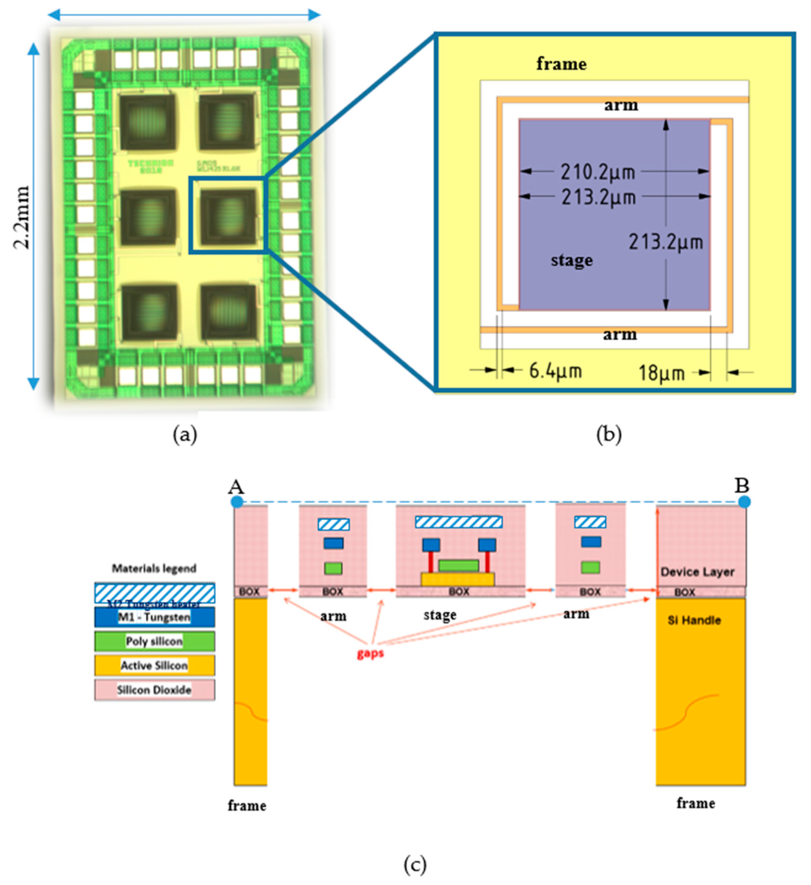
2. Hot Plate Operating in Air, with a Low Thermal Conductivity
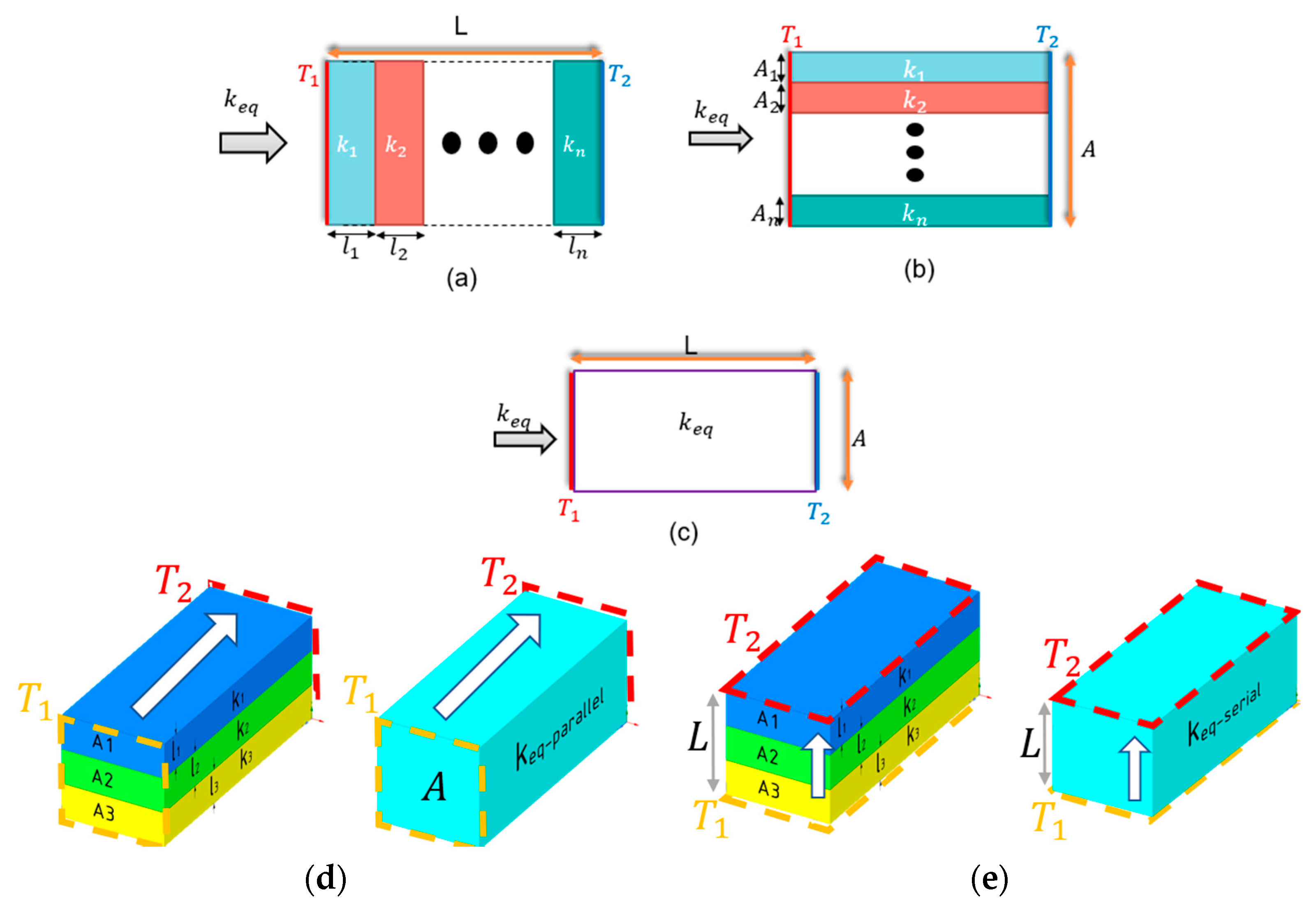
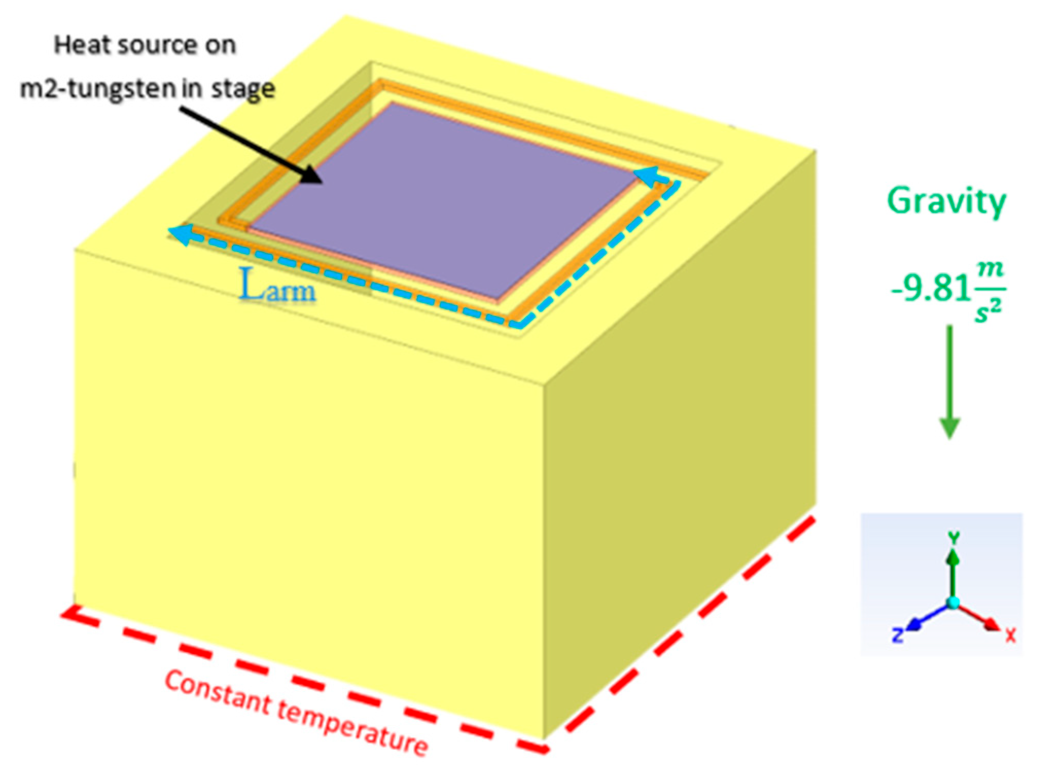
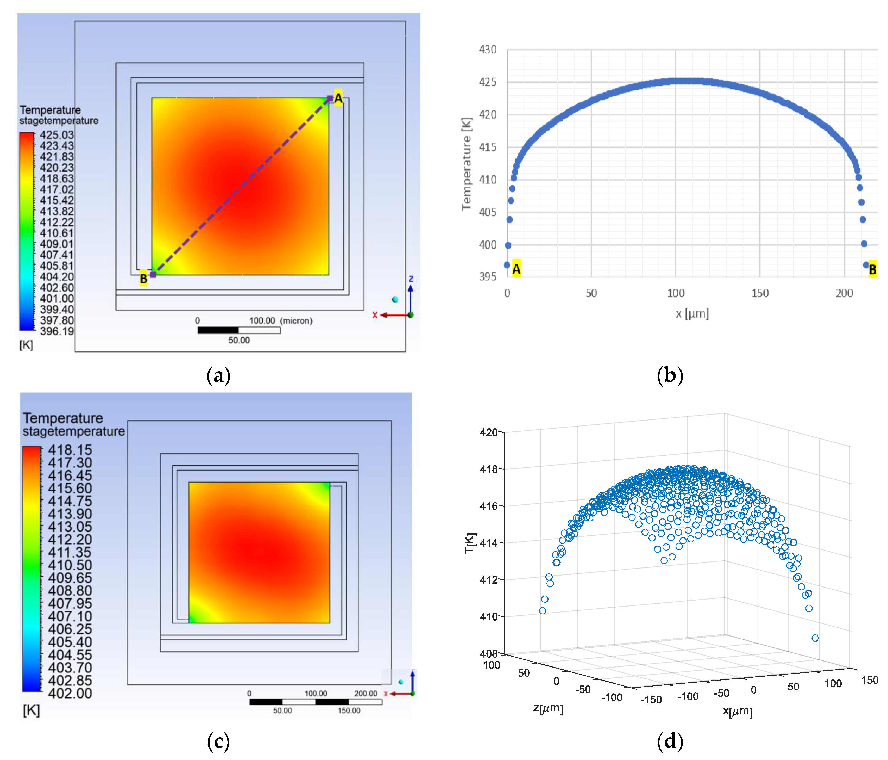
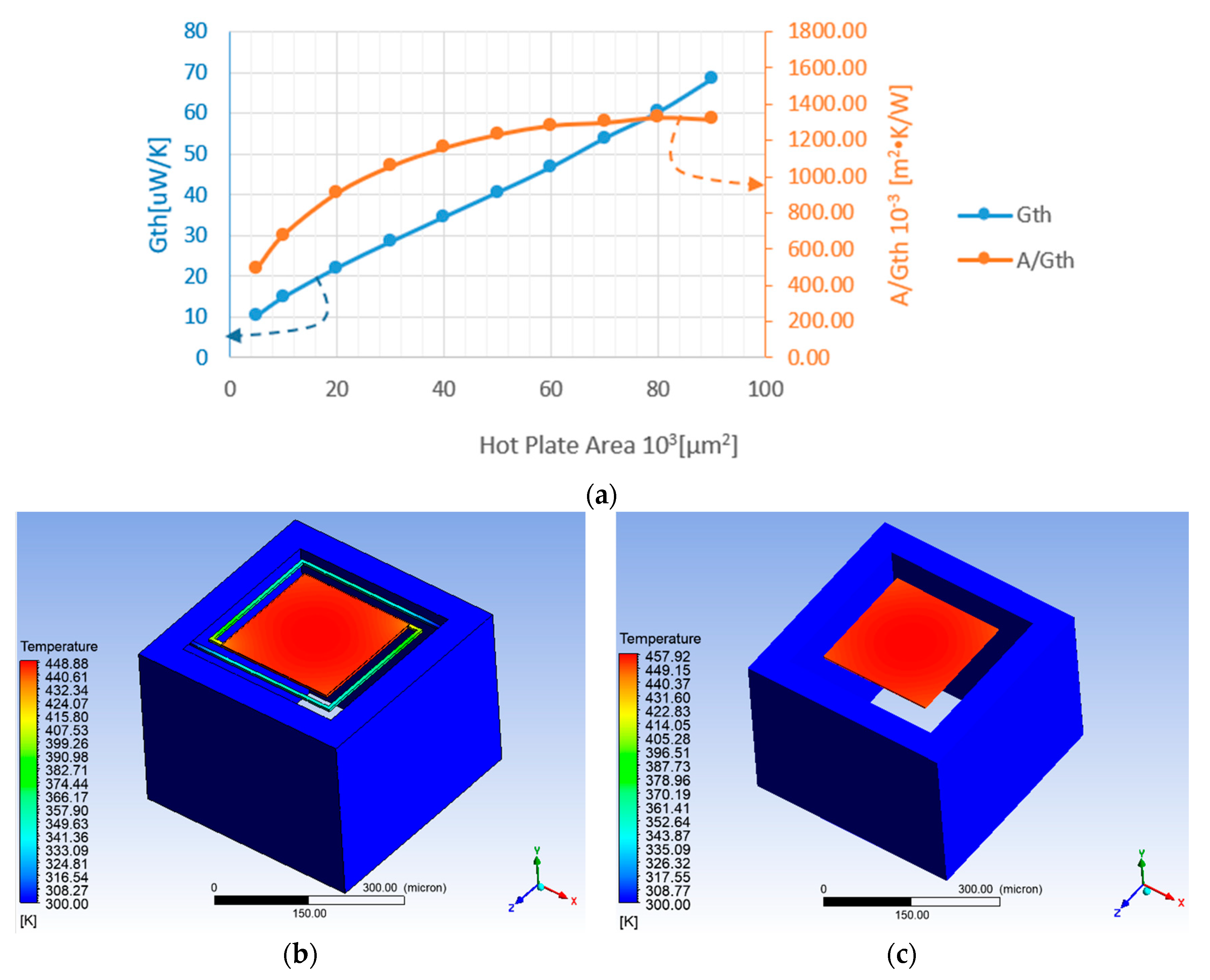
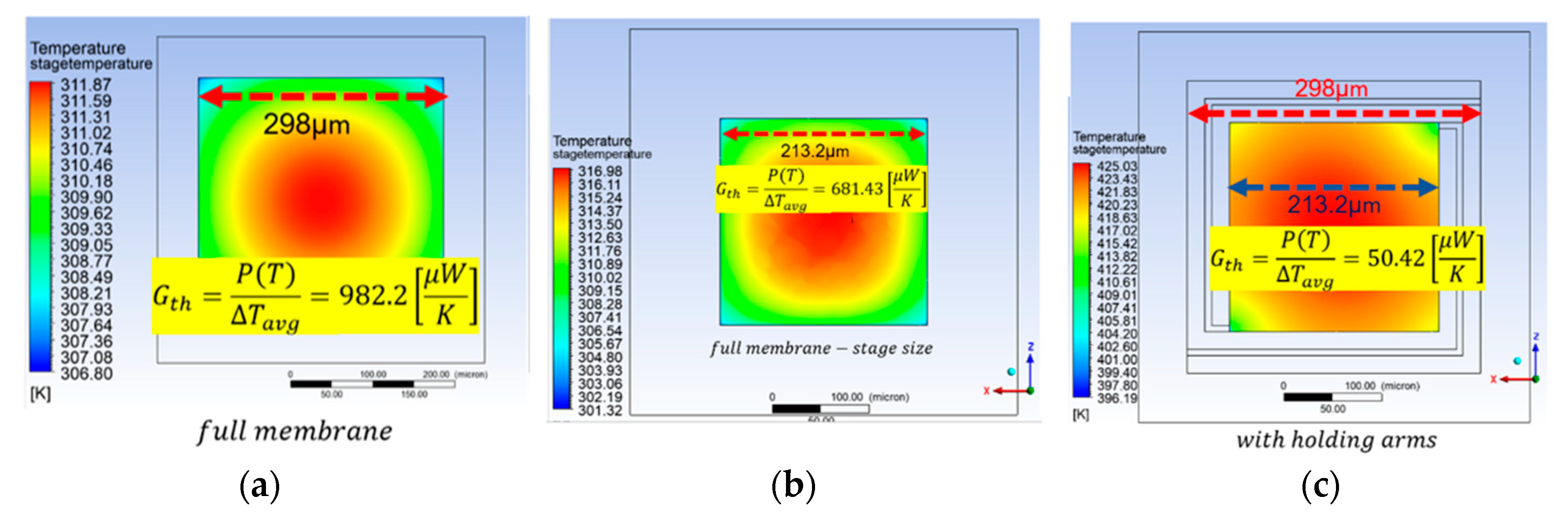
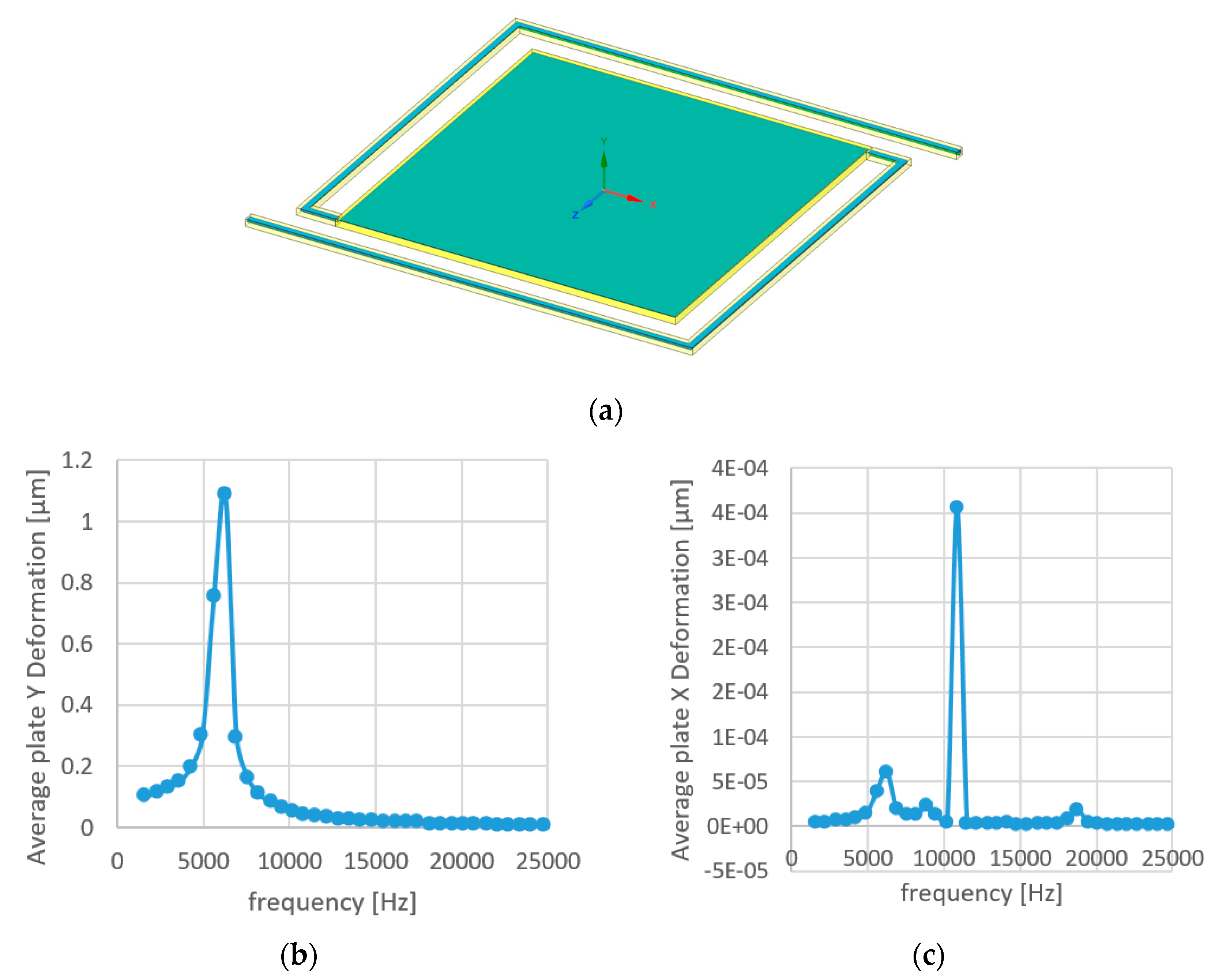
2.1. Modeling Supported by Simulations
2.2. Simulations Supported by Modeling
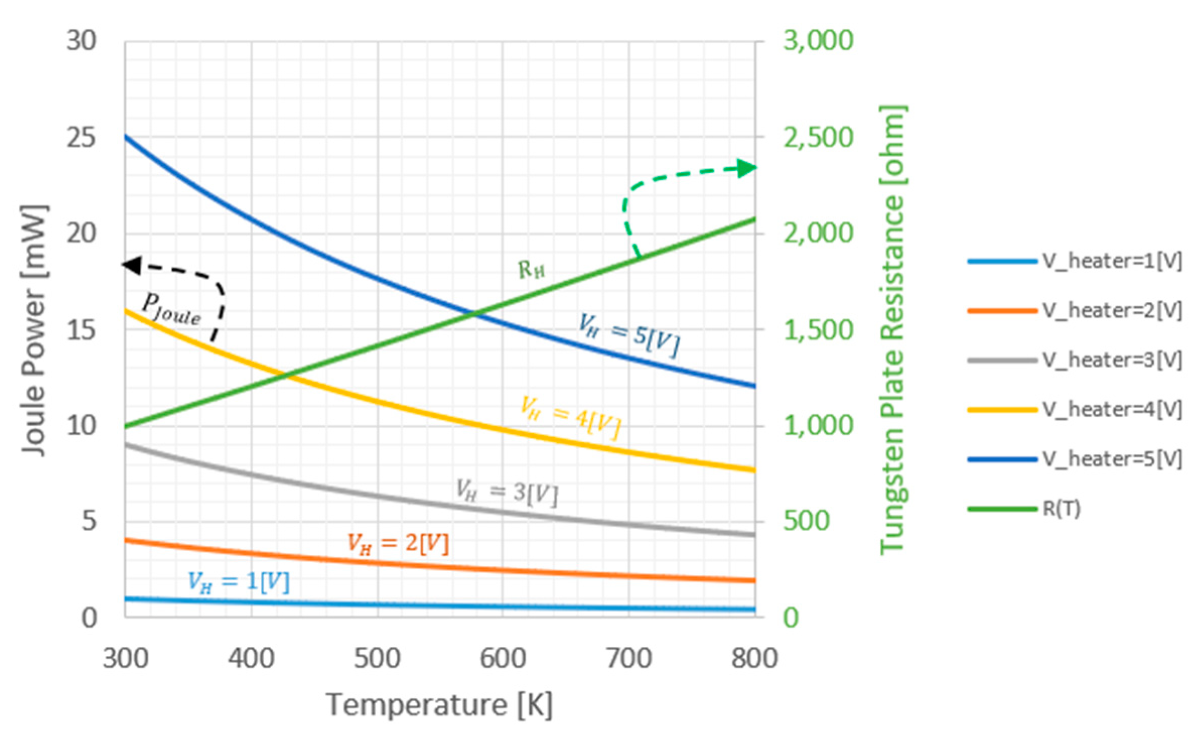
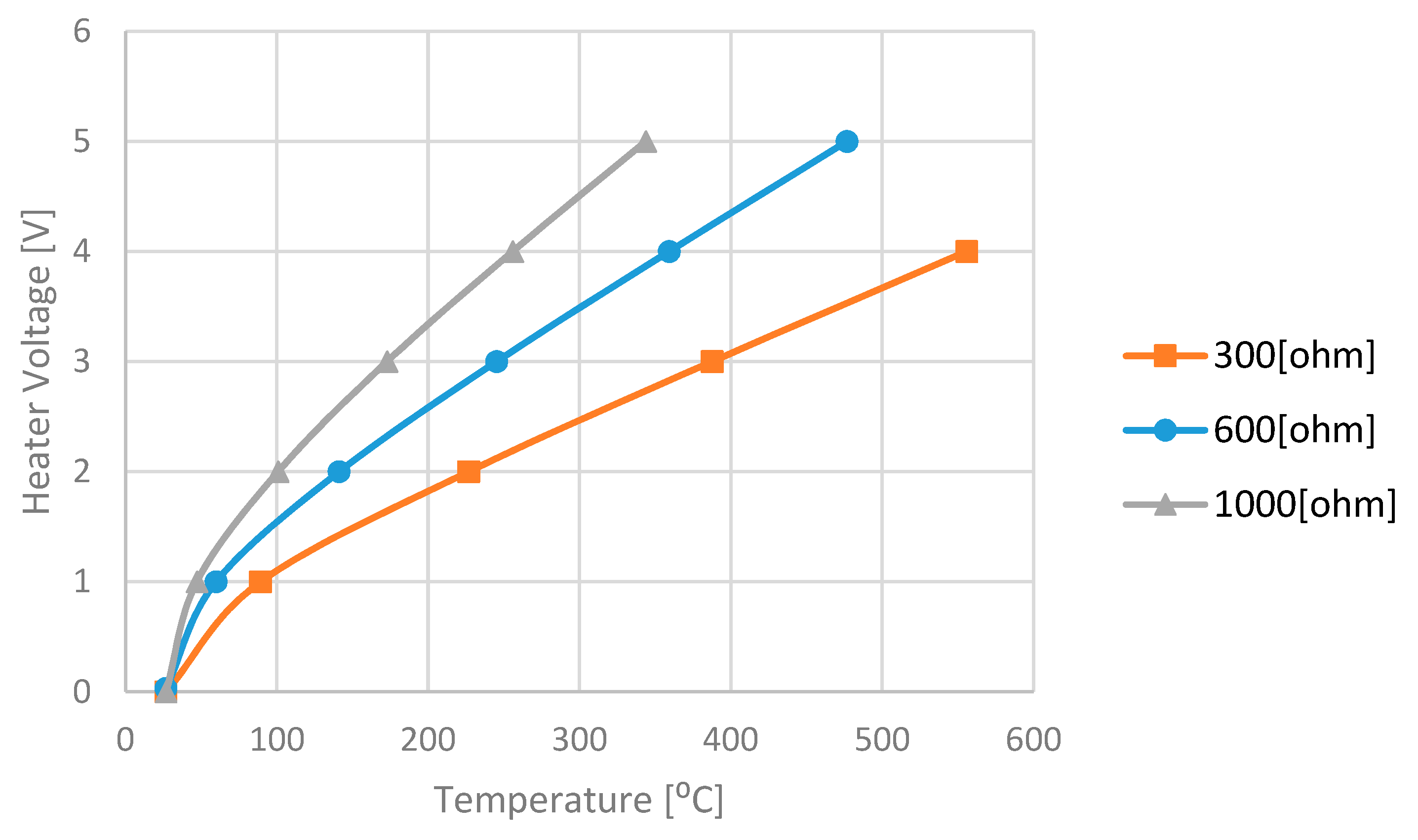
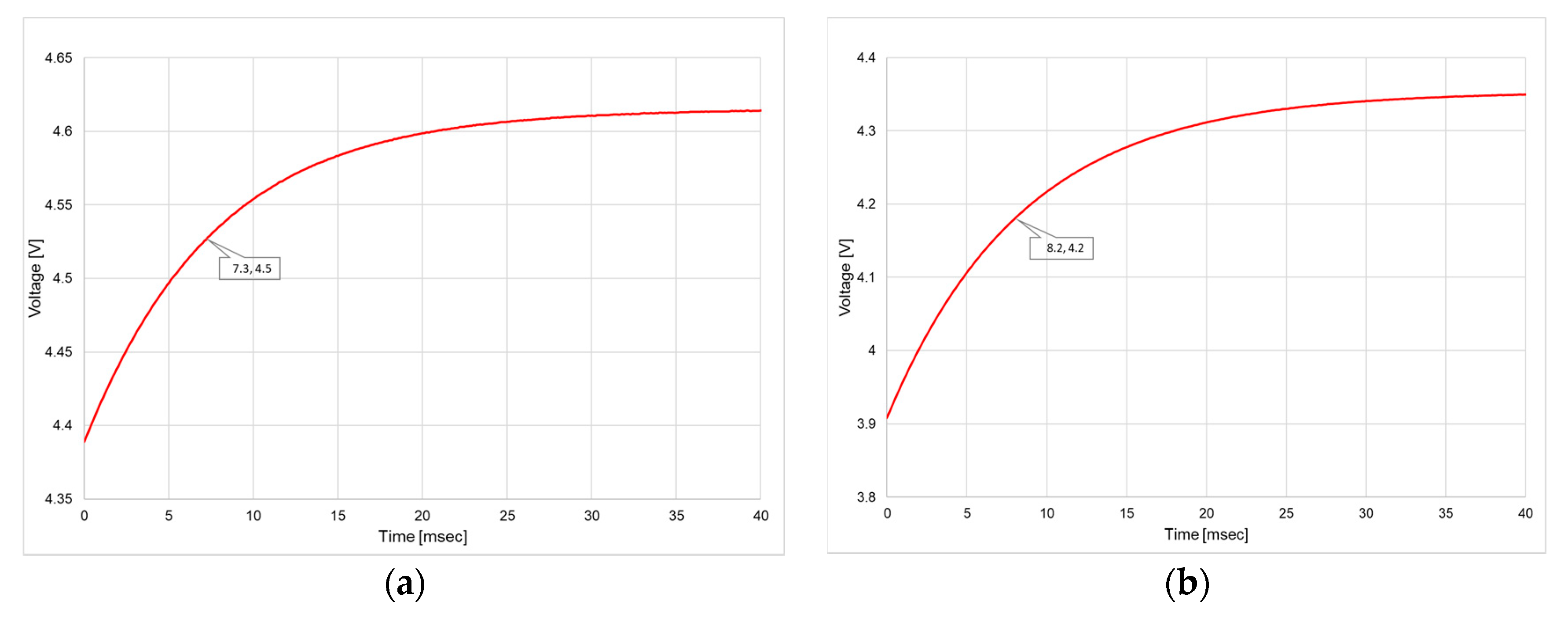
3. Measuring the Hot Plate Temperature during Operation
3.1. Background
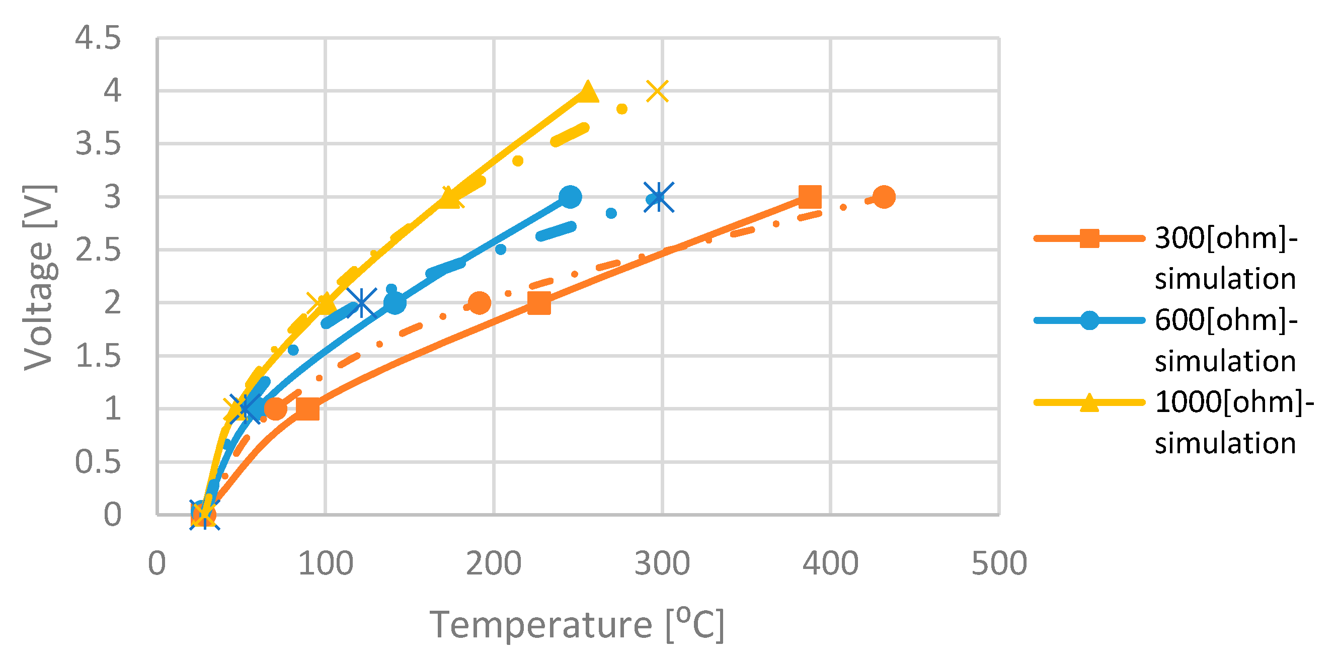
3.2. Analytical Modeling of the Measurements
3.3. Simulations
3.4. Measurement and Discussion
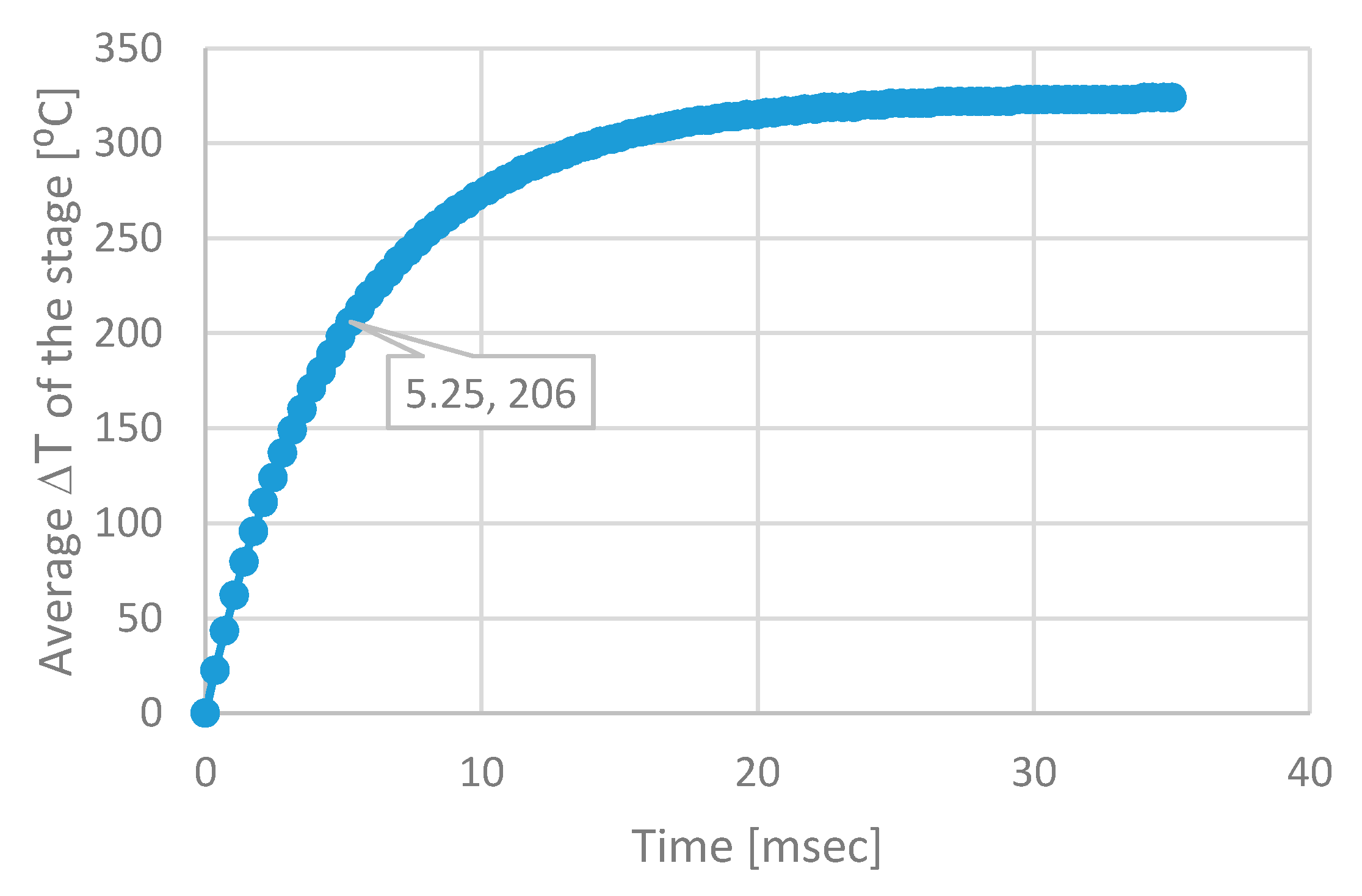
4. Reducing the Total Consumed Power during Operation by Applying Duty Cycle Operation
5. Conclusions
Author Contributions
Funding
Conflicts of Interest
References
- Fleischer, M.; Lehmann, M. Solid State Gas Sensors–Industrial Application (Springer Series on Chemical Sensors and Biosensors); Fleischer, M., Lehmann, M., Eds.; Springer: Berlin/Heidelberg, Germany, 2012; pp. 3–12. [Google Scholar] [CrossRef]
- Graf, M.; Barrettino, D.; Baltes, H.P.; Hierlemann, A. CMOS Hotplate Chemical Microsensors; Springer: Berlin/Heidelberg, Germany, 2007. [Google Scholar]
- Hierlemann, A. Integrated Chemical Microsensor Systems in CMOS Technology; Springer: Berlin/Heidelberg, Germany, 2005. [Google Scholar] [CrossRef]
- Gardner, J.W.; Guha, P.K.; Udrea, F.; Covington, J.A. CMOS interfacing for integrated gas sensors: A review. IEEE Sens. J. 2020, 10, 1833–1848. [Google Scholar] [CrossRef]
- Jaaniso, R.; Tan, O.K. Semiconductor Gas Sensors; Jaaniso, R., Tan, O.K., Eds.; Woodhead Publishing: Cambridge, UK, 2013. [Google Scholar]
- Ihokure, K.; Watson, J. The Stannic Oxide Gas Sensor Principles and Applications; CRC Press: Boca Raton, FL, USA, 1994. [Google Scholar] [CrossRef]
- Symons, E.A. Catalytic gas sensors. In Gas Sensors Principles, Operation and Developments, 1st ed.; Sberveglieri, G., Ed.; Springer: Dordrecht, The Netherlands, 1992; pp. 169–185. [Google Scholar]
- Miller, J.B. Catalytic sensors for monitoring explosive atmospheres. IEEE Sens. J. 2001, 1, 88–93. [Google Scholar] [CrossRef]
- Firth, J.G.; Jones, A.; Jones, T.A. The principles of the detection of flammable atmospheres by catalytic devices. Combust. Flame 1973, 20, 303–311. [Google Scholar] [CrossRef]
- Brauns, E.; Morsbach, E.; Kunz, S.; Bäumer, M.; Lang, W. A fast and sensitive catalytic gas sensor for hydrogen detection based on stabilized nanoparticles as catalytic layer. Sens. Actuators B 2014, 193, 895–903. [Google Scholar] [CrossRef]
- Bogue, R. Recent developments in MEMS sensors: A review of applications, markets and technologies. Sens. Rev. 2013, 33, 300–304. [Google Scholar] [CrossRef]
- Nemirovsky, Y.; Stolyarova, S.; Blank, T.; Svetlitza, A.; Bar-Lev, S.; Zviagintsev, A.; Brouk, I. A new pellistor-like gas sensor based on micromachined CMOS transistor. IEEE Trans. Electron. Devices 2018, 99, 5494–5498. [Google Scholar] [CrossRef]
- Nemirovsky, Y. Gas Sensing Device and a Method for Sensing Gas, TODOS-Technion. U.S. Patent Application No.20170205366, 20 July 2017. [Google Scholar]
- Nemirovsky, Y.; Nemirovsky, A.; Melman, S. GAS Sensing Device Having Distributed Gas Sensing Elements and a Method for Sensing Gas. U.S. Patent Application No. 20190011415, 10 January 2019. [Google Scholar]
- Shlenkevitch, D.; Avraham, M.; Stolyarova, S.; Blank, T.; Nemirovsky, Y. Catalytic gas sensor based on micro machined transistor. In Proceedings of the 2019 IEEE International Conference on Microwaves, Antennas, Communications and Electronic Systems COMCAS, Tel Aviv, Israel, 4–6 November 2019. [Google Scholar] [CrossRef]
- Shlenekvitch, D.; Stolyarova, S.; Blank, T.; Brouk, I.; Nemirovsky, Y. A novel miniature and selective CMOS gas sensor for gas mixture analysis—Part 1: Emphasis on Chemical Aspects. Micromachines 2020, 11, 345. [Google Scholar] [CrossRef] [PubMed] [Green Version]
- Gitelman, L.; Stolyarova, S.; Bar-Lev, S.; Gutman, Z.; Ochana, Y.; Nemirovsky, Y. CMOS-SOI-MEMS transistor for uncooled IR imaging. IEEE Trans. Electron. Devices 2009, 56, 1935–1942. [Google Scholar] [CrossRef]
- Nemirovsky, Y.; Svetlitza, A.; Brouk, I.; Stolyarova, S. Nanometric CMOS-SOI-NEMS transistor for uncooled THz sensing. IEEE Trans. Electron. Devices 2013, 60, 1575–1583. [Google Scholar] [CrossRef]
- Saraf, T.; Brouk, I.; Bar-Lev, S.; Unikovsky, A.; Blank, T.; Radhakrishnan, P.; Nemirovsky, Y. CMOS-SOI-MEMS uncooled infrared security sensor with integrated readout. IEEE J. Electron. Device Soc. 2016, 4, 155–162. [Google Scholar] [CrossRef]
- Zviagintsev, A.; Blank, T.; Brouk, I.; Bloom, I.; Nemirovsky, Y. Modeling the performance of nano machined CMOS transistors for uncooled IR sensing. IEEE Trans. Electron. Devices 2017, 64, 4657–4663. [Google Scholar] [CrossRef]
- Zviagintsev, T.; Blank, I.; Brouk, S.; Bar-Lev, S.; Stolyarova, A.; Svetlitza, I.B.; Nemirovsky, Y. Micro-machined CMOS-SOI transistor (TMOS) thermal sensor operating in air. In Proceedings of the IEEE COMCAS—International Conference on Microwaves, Communications, Antennas and Electronic Systems, Tel Aviv, Israel, 13–15 November 2017. [Google Scholar] [CrossRef]
- Avraham, M.; Shlenkevitch, D.; Stolyarova, S.; Blank, T.; Nemirovsky, Y. Modeling the thermal performance of a packaged MEMS thermal sensor at wide pressure range for IoT applications. In Proceedings of the 2019 IEEE International Conference on Microwaves, Antennas, Communications and Electronic Systems COMCAS, Tel Aviv, Israel, 4–6 November 2019. [Google Scholar] [CrossRef]
- Ansys Fluent. Available online: https://www.ansys.com/products/fluids/ansys-fluent (accessed on 1 June 2020).
- Bartholomew, C.H.; Farrauto, R.J. Catalyst Deactivation: Causes, Mechanisms, and Treatment, Fundamentals of Industrial Catalytic Processes, 2nd ed.; Wiley: New Jersey, NJ, USA, 2011; p. 293. [Google Scholar] [CrossRef]
- Grove, A.S. Physics and Technology of Semiconductor Devices; Wiley: New York, NY, USA, 1967. [Google Scholar]
- Frank, R. Semiconductor Junction Thermometer, in Spatial, Mechanical, Thermal, and Radiation Measurement; Webster, J.G., Eren, H., Eds.; Taylor & Francis Group: Boka Raton, FL, USA, 2014; ISBN 9781439848883. [Google Scholar]
- Williams, J. High performance signal conditioning for transducers. In Proceedings of the Sensors Expo West, San Jose, CA, USA, 2–4 March 1993. [Google Scholar]
- KJurgen, R. (Ed.) Automotive Electronics Handbook; McGraw-Hill: New York, NY, USA, 1999. [Google Scholar]
- Frank, R. Understanding Smart Sensors; ArtechHouse: Boston, MA, USA, 2013. [Google Scholar]
- Sze, S.M.; Ng, K.K. Physics of Semiconductor Devices; John Wiley & Sons, Inc.: Hoboken, NJ, USA, 2006. [Google Scholar]


| Property | Description | SiO2 | Poly Si | Si(c) | Tungsten | Platinum | Silicon Nitride |
|---|---|---|---|---|---|---|---|
| k [W/(mK)] | Thermal conductivity | 1.4 | 40 | 40 | 173 | 21,450 | 31 |
| CP [J/(kgK)] | Heat capacity at constant pressure | 730 | 700 | 700 | 134 | 126 | 1100 |
| [kg/m3] | Density | 2200 | 2320 | 2329 | 19,300 | 71.6 | 3250 |
| E [GPa] | Young’s modulus | 70 | 160 | - | 411 | - | - |
| Poisson’s ratio | 0.17 | 0.22 | - | 0.28 | - | - |
| Study Parameters | Value | Units |
|---|---|---|
| N | 2 | - |
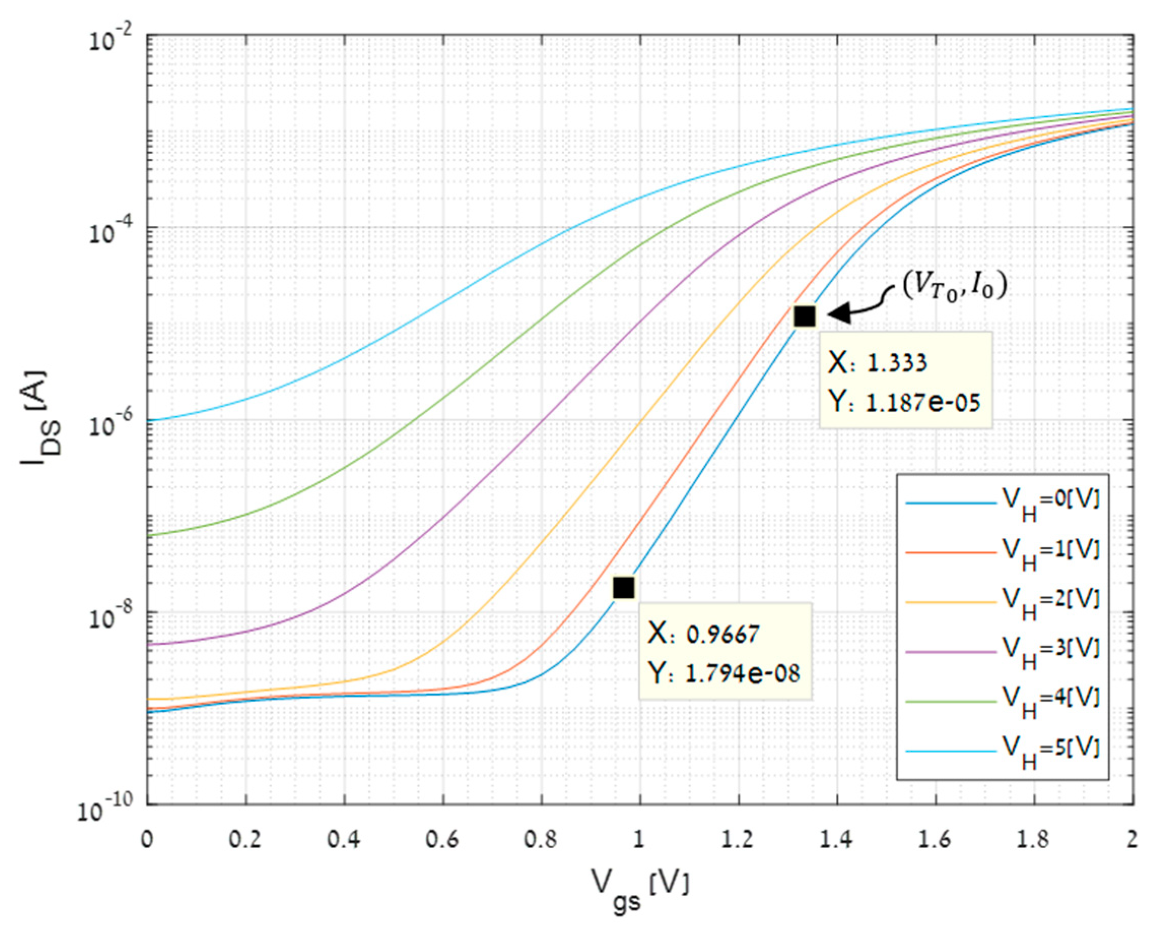
| dVt/dT | ||
| (from the graph when ) | 1.3 | V |
| 300 | K | |
| W/L | 1425 | - |
| 1000 | ||
| I0 (extracted from Figure 7) | A |
| Vheater (V) | 0 | 1 | 2 | 3 | 4 | 5 |
| Temperature (K) | 301.44 | 318.90 | 368.34 | 449.01 | 570.29 | 774.44 |
© 2020 by the authors. Licensee MDPI, Basel, Switzerland. This article is an open access article distributed under the terms and conditions of the Creative Commons Attribution (CC BY) license (http://creativecommons.org/licenses/by/4.0/).
Share and Cite
Avraham, M.; Stolyarova, S.; Blank, T.; Bar-Lev, S.; Golan, G.; Nemirovsky, Y. A Novel Miniature and Selective CMOS Gas Sensor for Gas Mixture Analysis—Part 2: Emphasis on Physical Aspects. Micromachines 2020, 11, 587. https://0-doi-org.brum.beds.ac.uk/10.3390/mi11060587
Avraham M, Stolyarova S, Blank T, Bar-Lev S, Golan G, Nemirovsky Y. A Novel Miniature and Selective CMOS Gas Sensor for Gas Mixture Analysis—Part 2: Emphasis on Physical Aspects. Micromachines. 2020; 11(6):587. https://0-doi-org.brum.beds.ac.uk/10.3390/mi11060587
Chicago/Turabian StyleAvraham, Moshe, Sara Stolyarova, Tanya Blank, Sharon Bar-Lev, Gady Golan, and Yael Nemirovsky. 2020. "A Novel Miniature and Selective CMOS Gas Sensor for Gas Mixture Analysis—Part 2: Emphasis on Physical Aspects" Micromachines 11, no. 6: 587. https://0-doi-org.brum.beds.ac.uk/10.3390/mi11060587