
Growth of a Large, Single-Crystalline WS2 Monolayer for High-Performance Photodetectors by Chemical Vapor Deposition

1
Hubei Engineering Technology Research Center of Energy Photoelectric Device and System, Hubei University of Technology, Wuhan 430068, China
2
Hubei Collaborative Innovation Center for High-Efficient Utilization of Solar Energy, Wuhan 430068, China
3
School of Science, Hubei University of Technology, Wuhan 430068, China
Micromachines 2021, 12(2), 137; https://0-doi-org.brum.beds.ac.uk/10.3390/mi12020137
Submission received: 17 December 2020
/
Revised: 19 January 2021
/
Accepted: 25 January 2021
/
Published: 27 January 2021
Abstract
:2D WS2 is a promising candidate for the next generation nanoelectronics, spintronics, valleytronics, and optoelectronics. However, the uncontrollably large-area growth of WS2 nanosheets and their unsatisfactory performance of the photodetectors based on WS2 hindered its applications. Here, we proposed a CVD method using tungstic acid as the precursors to grow WS2 flakes. After being characterized by AFM, Raman, PL, and TEM, we found the as-grown WS2 flakes were high-quality structures. Then the photodetectors based on the as-grown WS2 were fabricated, which exhibited high responsivity (7.3 A W−1), a fast response rate (a response time of 5 ms and a recovery time of 7 ms), prefect external quantum efficiency (EQE) (1814%), and remarkable detectivity (D*) (3.4 × 10¹² Jones). Our works provided a new CVD method to grow some high-quality WS2 nanosheets.
1. Introduction
Atomically thin tungsten disulfide (WS2), a 2D crystal with some interesting and important properties, is a promising candidate for the next generation of nanoelectronics, spintronics, valleytronics, and optoelectronics [1,2,3,4,5,6,7]. For example, WS2 has a direct bandgap in the visible range and high absorption relative to its thickness [5,8]. WS2 exhibits ambipolar field-modulation behavior [9]. The theoretical calculations predict that it has a reduced effective mass, allowing higher carrier mobility [10]. Monolayer WS2 has strong PL emission efficiency, stronger than other TMDCs [11,12]. WS2 exhibits strong spin-orbit coupling and band splitting due to spin enabling spintronics/valleytronics [13,14,15,16]. WS2 also has high nonlinear susceptibility, suggesting its use for nonlinear optical devices [17,18]. Nevertheless, most researchers on WS2 are largely limited because of the relatively small lateral size of exfoliated flakes, not to mention the randomness of their shape, thickness, and crystal quality [19,20]. Liquid exfoliation has an advantage for the mass production of WS2, but it is difficult to control defects, hindering its application to electronic devices [21,22,23]. CVD is a hopeful approach to grow large-area WS2 flakes for extensive device applications. There are two common methods to synthesize WS2 by supplying tungsten sources on inert substrates before sulfurization in CVD. One is thin tungsten films or thin tungsten oxide films deposited by various methods including e-beam evaporation, magnetron sputtering, and atomic layer deposition [11,24,25,26,27,28,29]. The other is that of tungsten oxides solid precursors vaporized with solid sulfur sources simultaneously during the CVD process [30,31,32,33,34]. As it is difficult to control the tungsten sources location, distribution, and uniformity precisely, and the poor adhesion of the sources to inert substrates, the controlled CVD growth of large-area uniform monolayer WS2 remains a challenge. Some groups used metal substrates (Au) instead of the inert substrates to synthesize a large-area monolayer WS2 film; they also tested the electrical properties of WS2-based field-effect transistors after bubbling transfer from Au substrates to SiO2/Si substrates [35,36,37]. Here we report a new method, spin-coating tungsten acid as a tungsten source on SiO2/Si substrates directly before sulfurization, to grow single crystalline WS2 monolayers with a size of up to hundreds of micrometers. We also found that photodetectors based on single crystalline WS2 flakes have a high responsivity of 7.3 A W−1 with a fast response rate of 5 ms, an external quantum efficiency (EQE) of 1814%, and a detectivity (D*) of 3.4 × 10¹² Jones.
2. Materials and Methods
The WS2 flakes were synthesized by using tungstic acid on SiO2/Si substrates as the precursors and sulfurizing via a chemical vapor deposition (CVD) method. First, 2.8 g of tungstic acid (99.9%, Alfa) was dispersed in the oxalic acid solution (0.15 M/L) by ultrasound. Then the tungstic acid colloidal solution was dispersed on a clean SiO2/Si substrate by spin-coating. After that, the whole substrate was annealed in air at 100 °C for 1h. Finally, the SiO2/Si substrates with tungstic acid were sulfurized by CVD. For CVD growth, the Si/SiO2 substrates with the tungstic acid colloidal solution were placed at the center of the quartz tube, and the 0.1 g S powders (99.5%, Alfa) were placed on the upstream side of the Si/SiO2 substrates. The quartz tube was flushed with Ar (5N) gas several times and purged to 0.1 Pa with a mechanical pump. The furnace temperature was raised to 900 °C in 30 min and kept for 30 min with a flow rate of 50 sccm Ar gas. After growth, the furnace was naturally cooled to room temperature. The synthesized WS2 samples were characterized by an atomic force microscope (AFM, SPM9700, Shimadzu), Raman spectroscopy, and a transmission electron microscope (TEM, Tecnai G2 F30 S-TWIN, FEI). The Raman spectra were recorded in the backscattering geometry at a 532 nm line with an argon ion laser Raman spectrometer (LabRAM HR800, Horiba JobinYvon). The Raman mappings were collected by alpha300 R, WITec GmbH, Ulm, Germany, the laser wavelength was 532 nm, and the scanning step interval was 300 nm.
We fabricated the photodetectors based on the WS2 flakes by a standard photolithography procedure (MDA-400M, Midas). The 10/50 nm Ti/Au electrode patterns were deposited by an E-beam deposition system (Nexdep, Angstrom Engineering). The photodetector measurement devices contained a broadband laser-driver light source (LDLS, EQ-1500, Energetiq) calibrated by a UV-enhanced silicon photodiode in an ambient atmosphere, a semiconductor characterization system (4200-SCS, Keithley), and an oscilloscope (DSO-X 3052A, Keysight). The oscilloscope light pulse chopped was 500 nm, and the frequency was 3 Hz.
3. Results and Discussion
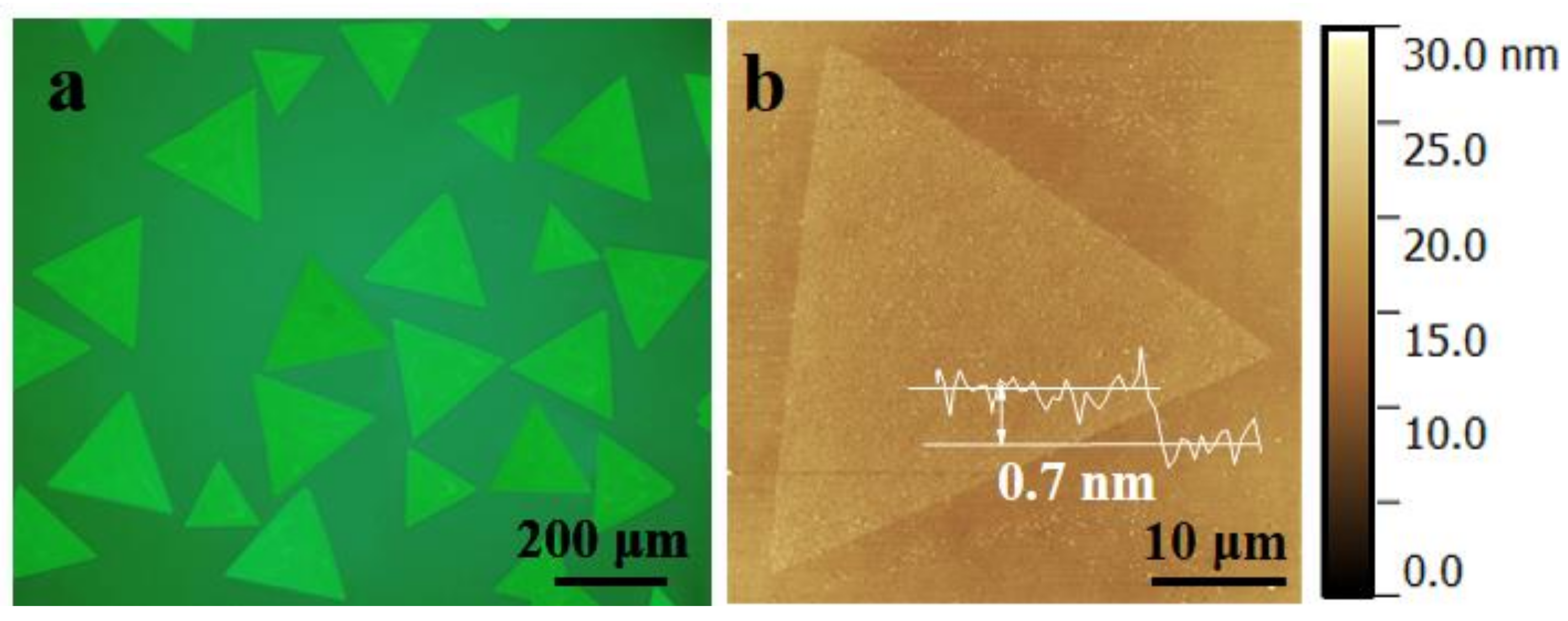
Figure 1a shows the optical image of the as-grown triangle WS2 flakes on SiO2/Si substrate; the majority of the flakes were more than 220 μm. The thickness of these triangle crystals was measured by atomic force microscopy (AFM) (Figure 1b). The AFM step height of the WS2 flake was typically measured at 0.7 nm, which corresponds to a one-layer structure.
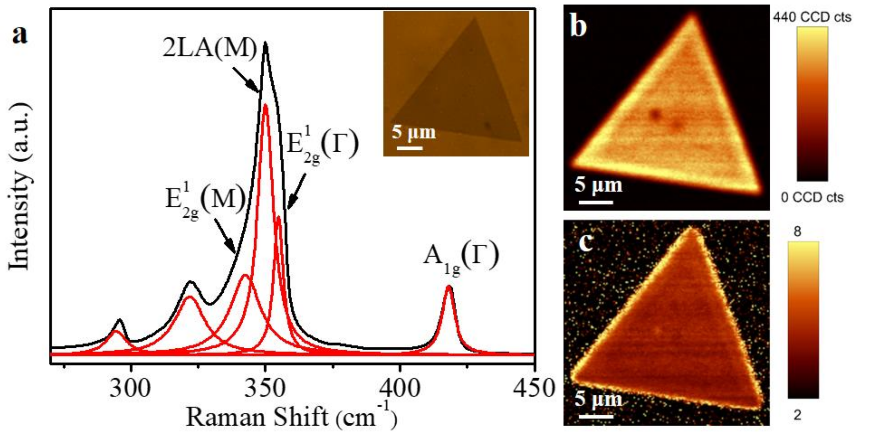
We have further investigated the layer number of the resulting atomically thin WS2 triangles by Raman spectroscopy. As shown in Figure 2a, the strongest peak of the WS2 triangle flake at about 350 cm−1 includes three subpeaks, which are resolved by a multipeak Lorentzian fitting. According to the calculated phonon dispersion [38] and experimental studies [13,39,40,41] of 1L-WS2, the in-plane vibrational E12g(M) mode peak is at 343 cm−1, the second-order mode of longitudinal acoustic phonon 2LA (M) peak is at 350 cm−1, and the in-plane vibrational E12g(Γ) mode peak is at 355 cm−1, respectively. The other peaks at 418, 295, and 322 cm−1 are attributed to the out-of-plane A1g(Γ) mode, the combination modes of 2LA(M)-2E22g(Γ), and the combination modes of 2LA(M)-E22g(Γ), respectively. The spectral fingerprint of a monolayer WS2 is the frequency separation of 62 cm−1 between the E12g(Γ) mode and the A1g(Γ) mode [11]. Raman images (Figure 2b,c) plotted by extracting the intensity were acquired to demonstrate the uniformity of our WS2 samples. The 2LA(M) phonon mode was much more intense than the A1g(Γ) mode. The as-grown WS2 triangle flake was uniform.
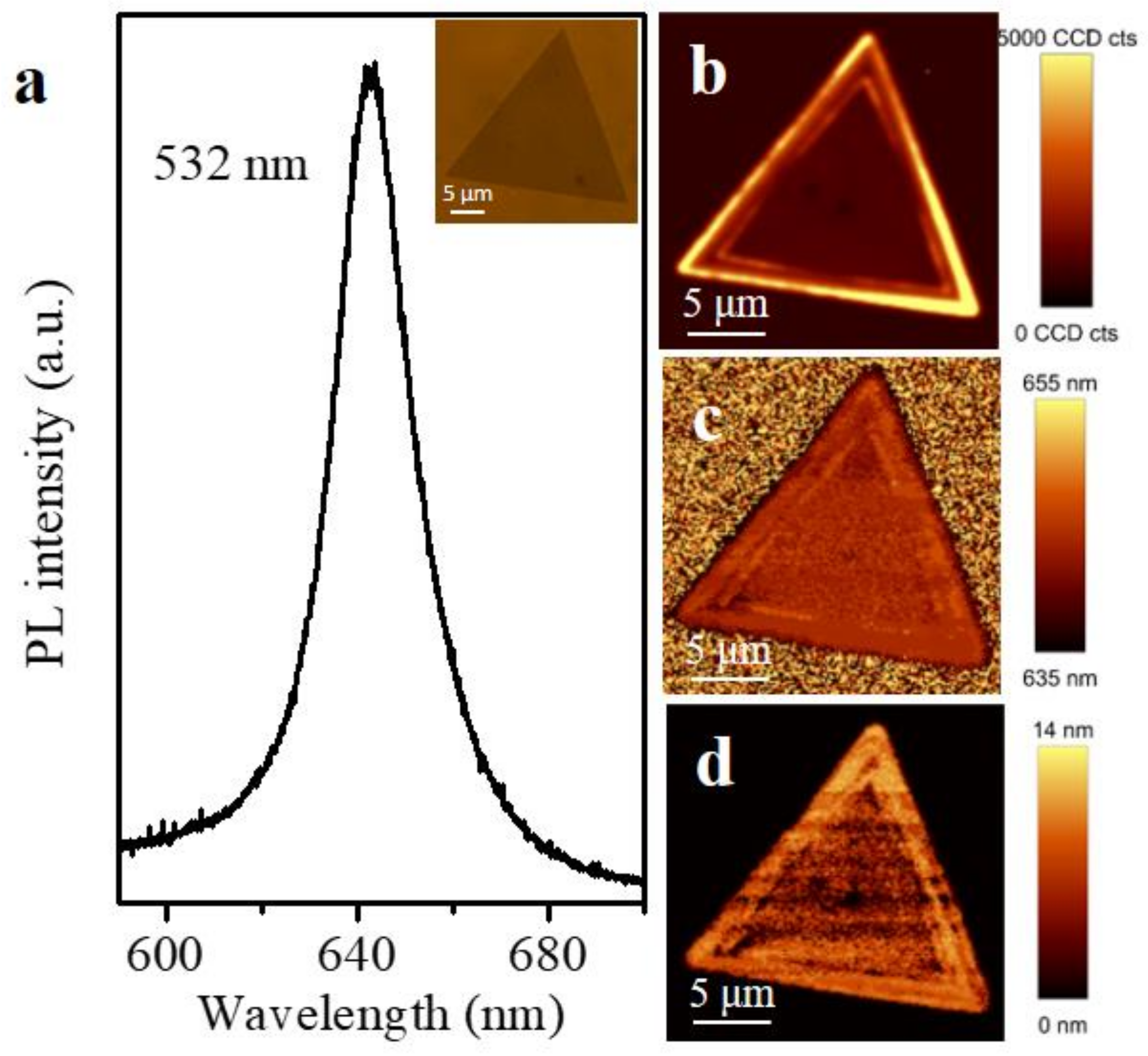
The optical properties of the monolayer WS2 triangle flakes were further investigated by microphotoluminescence (PL). The monolayer WS2 flake has a PL peak at about 642 nm, and its full width half maximum (FWHM) value is 22 nm (Figure 3a). The corresponding PL peak-integrated intensity, position, and width mappings of the monolayer WS2 triangle flake are shown in Figure 3b–d, respectively. The results of the PL indicated the as-grown WS2 was defect free and uniform.
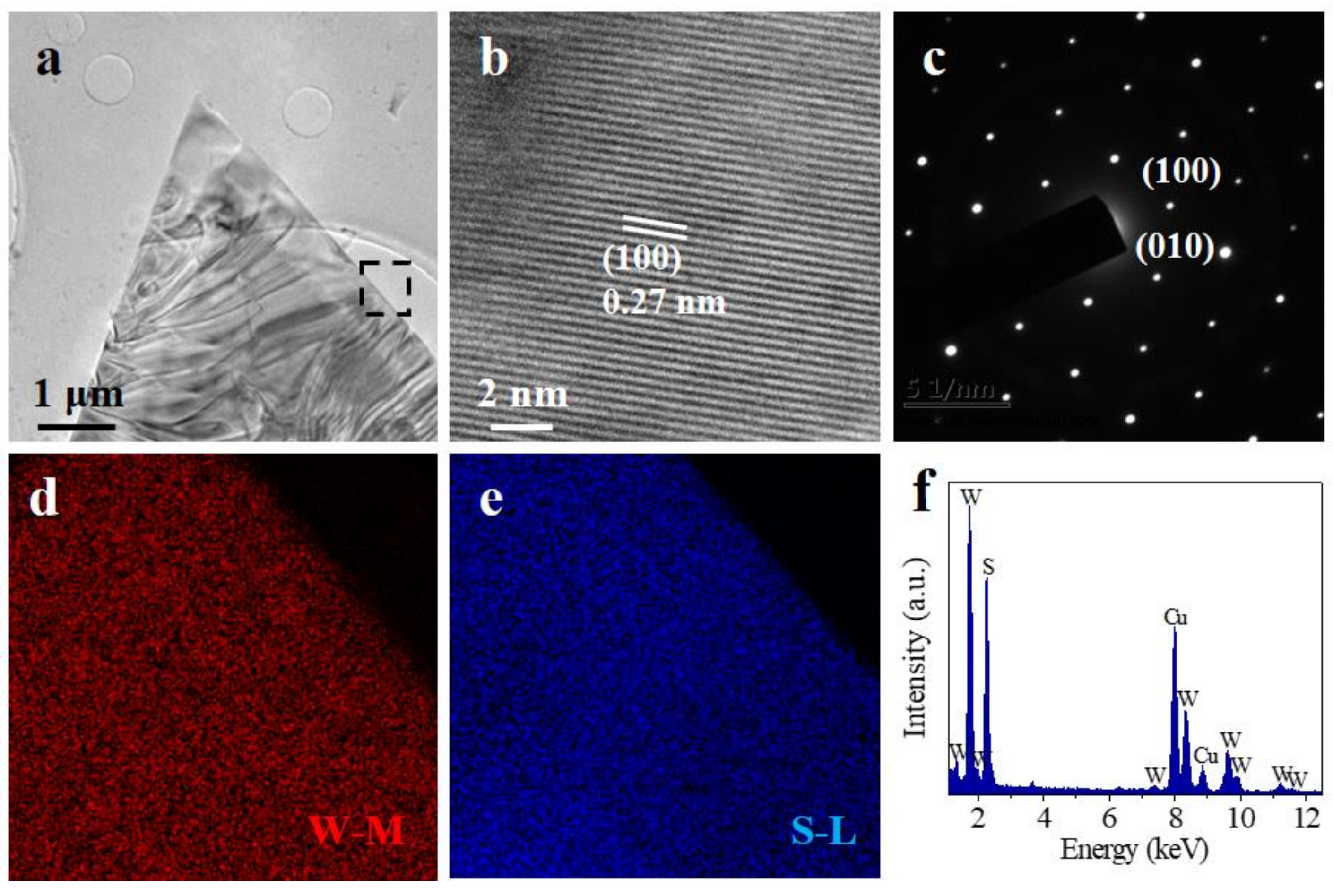
The structures of the monolayer WS2 triangle flakes were characterized by TEM. Figure 4a shows the low magnitude bright-field TEM image of a WS2 triangular crystal. The high-resolution TEM (HRTEM) image (Figure 4b) shows the hexagonal lattice fringes, which indicates a perfect atomic structure with a lattice spacing of 0.27 nm, corresponding to the (100) planes. The corresponding selected area electron diffraction (SAED) pattern (Figure 4c) revealed the defect free nature of the WS2 flake [36]. Then the elemental compositions of the WS2 triangle flakes were acquired by EDX mapping and EDX spectrum. EDX mapping in Figure 4d,e indicates the W and S elements distribute evenly. EDX spectrum in Figure 4f demonstrates the atomic ratio of W and S is around 1:2, which is consistent with the original stoichiometry of WS2. The TEM results further prove that as-grown WS2 flakes are defect free.
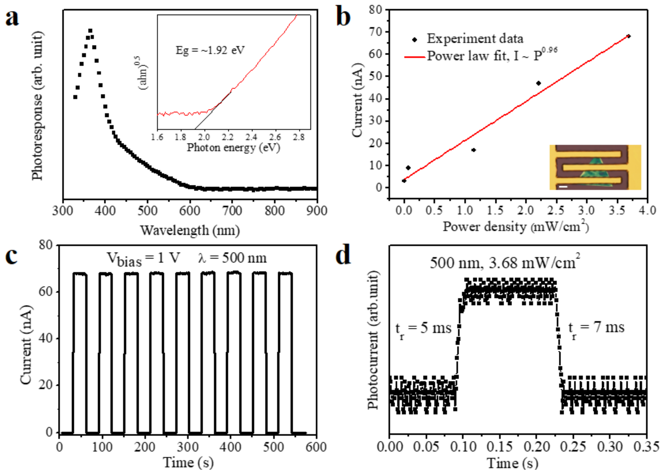
To research the optoelectronic properties of the WS2 flakes, photodetectors based on them were fabricated. The spectral response curve reaches a minimum at the wavelength of ≈645 nm in Figure 5a. Hence, the bandgap is about 1.92 eV by calculation, which is consistent with the PL results. Fitting the plot of photocurrent Iph on light intensity P for the WS2 flake as Iph ≈ Pθ obtains the value of θ ≈ 0.96 (Figure 5b), hinting the as-grown WS2 has very few defects or traps to photo-induced electron/hole pairs in the test power density range [42]. We further tested the cyclability of the photodetector under 500 nm incident light with the light on/off time interval of 30 s under a bias of 1 V (Figure 5c). The performances of the photodetector are stable. The response and recovery rates were 5 ms and 7 ms tested by an oscilloscope, respectively (Figure 5d). The photoresponsivity was 7.3 A W−1, according to the Rλ = Iph/PS, where Iph is the photoexcited current, P is the light power intensity, and S is the effective area of the photodetector. The external quantum efficiency (EQE) was 1814%, according to the EQE = hcRλ/eλ, where h is the Plank’s constant, c is the light velocity, Rλ is the photoresponsivity, e is the elementary electronic charge, and λ is the exciting wavelength. The specific detectivity (D*) was 3.4 × 10¹² Jones, according to the D* = RλS 1/2/(2eI dark)1/2, where I dark is the dark current. The performance of our photodetector is more inspiring than the most reported WS2 based photodetectors shown in Table 1.
4. Conclusions
In summary, we grew the monolayer WS2 triangle flakes via a CVD method with the tungstic acid, and researched the performance of the photodetectors based on them. The utilization of tungstic acid colloidal solution could improve the uniformity of the tungsten sources on the substrates. The as-grown monolayer WS2 flakes have a size of about 220 μm, a bandgap of about 1.92 eV, and no defects. The photodetectors based on them showed excellent performance, such as high responsivity of 7.3 A W−1, large EQE of 1814%, and a fast response rate of 5 ms.
Funding
This research was funded by the Natural Science Foundation of China, grant number 21701041; the Open Foundation of Hubei Collaborative Innovation Center for High-efficiency Utilization of Solar Energy, grant number HBSKFQN2017001; and the Talents of high-level scientific research foundation of the Hubei University of Technology, grant number BSQD2017010.
Institutional Review Board Statement
Not applicable.
Informed Consent Statement
Not applicable.
Data Availability Statement
No new data were created or analyzed in this study. Data sharing is not applicable to this article.
Conflicts of Interest
The authors declare no conflict of interest.
References
- Manzeli, S.; Ovchinnikov, D.; Pasquier, D.; Yazyev, O.V.; Kis, A. 2D transition metal dichalcogenides. Nat. Rev. Mater. 2017, 2, 17033. [Google Scholar] [CrossRef]
- Schmidt, H.; Giustiniano, F.; Eda, G. Electronic transport properties of transition metal dichalcogenide field-effect devices: Surface and interface effects. Chem. Soc. Rev. 2015, 44, 7715–7736. [Google Scholar] [CrossRef] [PubMed]
- Chhowalla, M.; Liu, Z.F.; Zhang, H. Two-dimensional transition metal dichalcogenide (TMD) nanosheets. Chem. Soc. Rev. 2015, 44, 2584–2586. [Google Scholar] [CrossRef] [PubMed]
- Perea-López, N.; Elías, A.L.; Berkdemir, A.; Castro-Beltran, A.; Gutiérrez, H.R.; Feng, S.; Lv, R.; Hayashi, T.; López-Urías, F.; Ghosh, S.; et al. Photosensor device based on few-layered WS2 films. Adv. Funct. Mater. 2013, 23, 5511–5517. [Google Scholar] [CrossRef]
- Eda, G.; Maier, S.A. Two-dimensional crystals: Managing light for optoelectronics. ACS Nano 2013, 7, 5660–5665. [Google Scholar] [CrossRef]
- Jeong, H.Y.; Jin, Y.; Yun, S.J.; Zhao, J.; Baik, J.; Keum, D.H.; Lee, H.S.; Lee, Y.H. Heterogeneous defect domains in single-crystalline hexagonal WS2. Adv. Mater. 2017, 29, 1605043. [Google Scholar] [CrossRef]
- Lan, C.Y.; Zhou, Z.Y.; Zhou, Z.F.; Li, C.; Shu, L.; Shen, L.F.; Li, D.P.; Dong, R.T.; Yin, S.P.; Ho, J.C. Wafer-scale synthesis of monolayer WS2 for high-performance flexible photodetectors by enhanced chemical vapor deposition. Nano Res. 2018, 11, 3371–3384. [Google Scholar] [CrossRef]
- Zhou, B.; Yang, L.X.; Chen, F.; Xu, M.; Wu, T.; Wu, G.; Chen, X.H.; Feng, D.L. Evolution of electronic structure in Eu1−xLaxFe2As2. J. Phys. Chem. Solids 2011, 72, 474478. [Google Scholar] [CrossRef]
- Sik Hwang, W.; Remskar, M.; Yan, R.; Protasenko, V.; Tahy, K.; Doo Chae, S.; Zhao, P.; Konar, A.; Xing, H.; Seabaugh, A.; et al. Transistors with chemically synthesized layered semiconductor WS2 exhibiting 105 room temperature modulation and ambipolar behavior. Appl. Phys. Lett. 2012, 101, 13107. [Google Scholar] [CrossRef] [Green Version]
- Liu, L.; Kumar, S.B.; Ouyang, Y.; Guo, J. Performance limits of monolayer transition metal dichalcogenide transistors. IEEE Trans. Electron Dev. 2011, 58, 3042–3047. [Google Scholar] [CrossRef] [Green Version]
- Gutierrez, H.R. Extraordinary room-temperature photoluminescence in triangular WS2 monolayers. Nano Lett. 2013, 13, 3447–3454. [Google Scholar] [CrossRef] [PubMed] [Green Version]
- Zhao, W.J. Evolution of electronic structure in atomically thin sheets of WS2 and WSe2. ACS Nano 2013, 7, 791–797. [Google Scholar] [CrossRef] [PubMed] [Green Version]
- Zeng, H.; Liu, G.B.; Dai, J.; Yan, Y.; Zhu, B.; He, R.; Xie, L.; Xu, S.; Chen, X.; Yao, W.; et al. Optical signature of symmetry variations and spin-valley coupling in atomically thin tungsten dichalcogenides. Sci. Rep. 2013, 3, 1608. [Google Scholar] [CrossRef] [Green Version]
- Xiao, D.; Liu, G.B.; Feng, W.; Xu, X.; Yao, W. Coupled spin and valley physics in monolayers of MoS2 and other group-VI dichalcogenides. Phys. Rev. Lett. 2012, 108, 196802. [Google Scholar] [CrossRef] [PubMed] [Green Version]
- Cao, T.; Wang, G.; Han, W.; Ye, H.; Zhu, C.; Shi, J.; Niu, Q.; Tan, P.; Wang, E.; Liu, B.; et al. Valley-selective circular dichroism of monolayer molybdenum disulphide. Nat. Commun. 2012, 3, 887. [Google Scholar] [CrossRef] [Green Version]
- Zhu, Z.Y.; Cheng, Y.C.; Schwingenschlögl, U. Giant spin-orbit-induced spin splitting in two-dimensional transition-metal dichalcogenide semiconductors. Phys. Rev. B 2011, 84, 153402. [Google Scholar] [CrossRef] [Green Version]
- Janisch, C.; Mehta, N.; Ma, D.; Elías, A.L.; Perea-López, N.; Terrones, M.; Liu, Z. Ultrashort optical pulse characterization using WS2 monolayers. Opt. Lett. 2014, 39, 383–385. [Google Scholar] [CrossRef]
- Janisch, C.; Wang, Y.; Ma, D.; Mehta, N.; Elías, A.L.; Perea-López, N.; Terrones, M.; Crespi, V.; Liu, Z. Extraordinary second harmonic generation in tungsten disulfide monolayers. Sci. Rep. 2014, 4, 5530. [Google Scholar] [CrossRef] [Green Version]
- Georgiou, T.; Yang, H.; Jalil, R.; Chapman, J.; Novoselov, K.S.; Mishchenko, A. Electrical and optical characterization of atomically thin WS2. Dalton Trans. 2014, 43, 10388–10391. [Google Scholar] [CrossRef]
- Ovchinnikov, D.; Allain, A.; Huang, Y.S.; Dumcenco, D.; Kis, A. Electrical transport properties of single-layer WS2. ACS Nano 2014, 8, 8174–8181. [Google Scholar] [CrossRef]
- Chhowalla, M. The chemistry of two-dimensional layered transition metal dichalcogenide nanosheets. Nature Chem. 2013, 5, 263–275. [Google Scholar] [CrossRef] [PubMed]
- Coleman, J.N.; Lotya, M.; O’Neill, A.; Bergin, S.D.; King, P.J.; Khan, U.; Young, K.; Gaucher, A.; De, S.; Smith, R.J.; et al. Two-dimensional nanosheets produced by liquid exfoliation of layered materials. Science 2011, 331, 568–571. [Google Scholar] [CrossRef] [PubMed] [Green Version]
- Nicolosi, V.; Chhowalla, M.; Kanatzidis, M.G.; Strano, M.S.; Coleman, J.N. Liquid exfoliation of layered materials. Science 2013, 340, 1226419. [Google Scholar] [CrossRef] [Green Version]
- Song, J.G.; Park, J.; Lee, W.; Choi, T.; Jung, H.; Lee, C.W.; Hwang, S.H.; Myoung, J.M.; Jung, J.H.; Kim, S.H.; et al. Layer-controlled, wafer-scale, and conformal synthesis of tungsten disulfide nanosheets using atomic layer deposition. ACS Nano 2013, 7, 11333–11340. [Google Scholar] [CrossRef] [PubMed]
- Orofeo, C.M.; Suzuki, S.; Sekine, Y.; Hibino, H. Scalable synthesis of layer-controlled WS2 and MoS2 sheets by sulfurization of thin metal films. Appl. Phys. Lett. 2014, 105, 83112. [Google Scholar] [CrossRef]
- Elías, A.L.; Perea-López, N.; Castro-Beltrán, A.; Berkdemir, A.; Lv, R.; Feng, S.; Long, A.D.; Hayashi, T.; Kim, Y.A.; Endo, M.; et al. Controlled synthesis and transfer of large-area WS2 Sheets: From single layer to few layers. ACS Nano 2013, 7, 5235–5242. [Google Scholar] [CrossRef]
- Jung, Y.; Shen, J.; Liu, Y.; Woods, J.M.; Sun, Y.; Cha, J.J. Metal seed layer thickness-induced transition from vertical to horizontal growth of MoS2 and WS2. Nano Lett. 2014, 14, 6842–6849. [Google Scholar] [CrossRef]
- Morrish, R.; Haak, T.; Wolden, C.A. Low-Temperature Synthesis of n-type WS2 thin films via H2S plasma sulfurization of WO3. Chem. Mater. 2014, 26, 3986–3992. [Google Scholar] [CrossRef]
- Zhou, S.; Liu, L.; Cui, S.; Ping, X.; Hu, D.; Jiao, L. Fast growth of large single-crystalline WS2 monolayers via chemical vapor deposition. Nano Res. 2020. [Google Scholar] [CrossRef]
- Fu, Q.; Wang, W.; Yang, L.; Huang, J.; Zhang, J.; Xiang, B. Controllable synthesis of high quality monolayer WS2 on a SiO2/Si substrate by chemical vapor deposition. RSC Adv. 2015, 5, 15795–15799. [Google Scholar] [CrossRef]
- Zhang, Y.; Zhang, Y.; Ji, Q.; Ju, J.; Yuan, H.; Shi, J.; Gao, T.; Ma, D.; Liu, M.; Chen, Y.; et al. Controlled growth of high-quality monolayer WS2 layers on sapphire and imaging its grain boundary. ACS Nano 2013, 7, 8963–8971. [Google Scholar] [CrossRef] [PubMed]
- Cong, C.; Shang, J.; Wu, X.; Cao, B.; Peimyoo, N.; Qiu, C.; Sun, L.; Yu, T. Synthesis and optical properties of large-area single-crystalline 2D semiconductor WS2 monolayer from chemical vapor deposition. Adv. Opt. Mater. 2014, 2, 131–136. [Google Scholar] [CrossRef]
- Okada, M.; Sawazaki, T.; Watanabe, K.; Taniguch, T.; Hibino, H.; Shinohara, H.; Kitaura, R. Direct chemical vapor deposition growth of WS2 atomic layers on hexagonal boron nitride. ACS Nano 2014, 8, 8273–8277. [Google Scholar] [CrossRef] [PubMed]
- Han, J.; Fang, R.; Zhu, L.; Geng, Z.; He, X. CVD growth of monolayer WS2 through controlled growth temperature and time. Ferroelectrics 2020, 562, 51–57. [Google Scholar] [CrossRef]
- Yun, S.J.; Chae, S.H.; Kim, H.; Park, J.C.; Park, J.H.; Han, G.H.; Lee, J.S.; Kim, S.M.; Oh, H.M.; Seok, J.; et al. Synthesis of centimeter-scale monolayer tungsten disulfide film on gold foils. ACS Nano 2015, 9, 5510–5519. [Google Scholar] [CrossRef]
- Gao, Y.; Liu, Z.; Sun, D.M.; Huang, L.; Ma, L.P.; Yin, L.C.; Ma, T.; Zhang, Z.; Ma, X.L.; Peng, L.M.; et al. Large-area synthesis of high-quality and uniform monolayer WS2 on reusable Au foils. Nat. Commun. 2015, 6, 8569. [Google Scholar] [CrossRef] [PubMed]
- Zhang, Y.; Shi, J.; Han, G.; Li, M.; Ji, Q.; Ma, D.; Zhang, Y.; Li, C.; Lang, X.; Zhang, Y.; et al. Chemical vapor deposition of monolayer WS2 nanosheets on Au foils toward direct application in hydrogen evolution. Nano Res. 2015, 8, 2881–2890. [Google Scholar] [CrossRef]
- Molina-Sánchez, A.; Wirtz, L. Phonons in single-layer and few-layer MoS2 and WS2. Phys. Rev. B 2011, 84, 155413. [Google Scholar] [CrossRef] [Green Version]
- Lee, Y.H.; Yu, L.; Wang, H.; Fang, W.; Ling, X.; Shi, Y.; Lin, C.T.; Huang, J.K.; Chang, M.T.; Chang, C.S.; et al. Synthesis and transfer of single-layer transition metal disulfides on diverse surfaces. Nano Lett. 2013, 13, 1852–1857. [Google Scholar] [CrossRef]
- Berkdemir, A.; Gutierrez, H.R.; Botello-Mendez, A.R.; Perea-Lopez, N.; Elias, A.L.; Chia, C.I.; Wang, B.; Crespi, V.H.; Lopez-Urias, F.; Charlier, J.C.; et al. Identification of individual and few layers of WS2 using Raman Spectroscopy. Sci. Rep. 2013, 3, 1755. [Google Scholar] [CrossRef] [Green Version]
- Zhao, W.; Ghorannevis, Z.; Amara, K.K.; Pang, J.R.; Toh, M.; Zhang, X.; Kloc, C.; Tan, P.H.; Eda, G. Lattice dynamics in mono- and few-layer sheets of WS2 and WSe2. Nanoscale 2013, 5, 9677–9683. [Google Scholar] [CrossRef] [PubMed] [Green Version]
- Kind, H.; Yan, H.Q.; Messer, B.; Law, M.; Yang, P.D. Nanowire ultraviolet photodetectors and optical switches. Adv. Mater. 2002, 14, 158–160. [Google Scholar] [CrossRef]
- Huo, N.J.; Yang, S.X.; Wei, Z.M.; Li, S.S.; Xia, J.B.; Li, J.B. Photoresponsive and gas sensing field-effect transistors based on multilayer WS2 nanoflakes. Sci. Rep. 2014, 4, 5209. [Google Scholar] [CrossRef] [PubMed] [Green Version]
- Lan, C.Y.; Li, C.; Yin, Y.; Liu, Y. Large-area synthesis of monolayer WS2 and its ambient-sensitive photo-detecting performance. Nanoscale 2015, 7, 5974–5980. [Google Scholar] [CrossRef] [PubMed]
- Yao, J.D.; Zheng, Z.Q.; Shao, J.M.; Yang, G.W. Stable, highly-responsive and broadband photodetection based on large-area multilayered WS2 films grown by pulsed-laser deposition. Nanoscale 2015, 7, 14974–14981. [Google Scholar] [CrossRef]
- Chen, Y.; Gan, L.; Li, H.; Ma, Y.; Zhai, T.Y. Achieving uniform monolayer transition metal dichalcogenides film on silicon wafer via silanization treatment: A typical study on WS2. Adv. Mater. 2017, 29, 1603550. [Google Scholar] [CrossRef]
- Harith, A.; Haroon, R. 405 nm ultraviolet photodetector based on tungsten disulphide thin film grown by drop casting method. J. Mod. Optic. 2019, 66, 1836–1840. [Google Scholar] [CrossRef]
Figure 1.
(a) Optical microscope images of the monolayer WS2. (b) AFM images of the monolayer WS2.

Figure 2.
(a) Raman characterization of the monolayer WS2 triangle flake with 532 nm excitation wavelengths. (b) A1g(Γ) intensity mapping for the WS2 triangle flake. (c) Intensity ratio mapping of 2LA(M) over A1g(Γ) for the WS2 triangle flake.
Figure 2.
(a) Raman characterization of the monolayer WS2 triangle flake with 532 nm excitation wavelengths. (b) A1g(Γ) intensity mapping for the WS2 triangle flake. (c) Intensity ratio mapping of 2LA(M) over A1g(Γ) for the WS2 triangle flake.

Figure 3.
(a) PL spectra of the monolayer WS2 triangle flake. (b–d) PL images of the peak integrated intensity, position, and width, respectively.
Figure 3.
(a) PL spectra of the monolayer WS2 triangle flake. (b–d) PL images of the peak integrated intensity, position, and width, respectively.

Figure 4.
(a) Low-magnification TEM image of the WS2 triangle flake. (b) High-resolution TEM image and (c) SAED pattern image of the WS2 triangle flake. (d,e) W and S elemental mapping in the black rectangle region of the WS2 flake in (a,f) EDX spectrum of the WS2 flake.
Figure 4.
(a) Low-magnification TEM image of the WS2 triangle flake. (b) High-resolution TEM image and (c) SAED pattern image of the WS2 triangle flake. (d,e) W and S elemental mapping in the black rectangle region of the WS2 flake in (a,f) EDX spectrum of the WS2 flake.

Figure 5.
Optoelectronic properties of the WS2 triangle flake. (a) The spectral response curve of the WS2 triangle flake. Inset: the fitting curve of obtaining the bandgap. (b) Photocurrent as a function of illumination intensity at Vbias = 1 V. Inset: the optical image of the WS2 photodetector; the scale bar is 10 μm. (c) Time-resolved photoresponse of the WS2 photodetector under a bias voltage of 1 V and illumination power of 3.68 mW·cm−2. (d) Response and recovery curves.


Table 1.
Comparison of the key parameters of our photodetector.
| Photodetectors | Fabrication Method | Rλ (A/W) | EQE (%) | Response Time (ms) | Reference |
|---|---|---|---|---|---|
| Multilayer WS2 | CVD | 92 × 10−6 | - | 5.3 | [4] |
| Multilayer WS2 | Exfoliated | 5.7 | 1118 | <20 | [43] |
| Monolayer WS2 | CVD | 18.8 × 10⁻³ | - | <4.5 | [44] |
| Multilayer WS2 | PLD | 0.51 | 137 | 4.1 × 10⁻³ | [45] |
| Monolayer WS2 | CVD | 3.07 | 763 | 370 | [46] |
| Multilayer WS2 | Drop casting | 145 × 10−3 | - | 153.78 | [47] |
| Monolayer WS2 | CVD | 7.3 | 1814 | 5 | This work |
Publisher’s Note: MDPI stays neutral with regard to jurisdictional claims in published maps and institutional affiliations. |
© 2021 by the author. Licensee MDPI, Basel, Switzerland. This article is an open access article distributed under the terms and conditions of the Creative Commons Attribution (CC BY) license (http://creativecommons.org/licenses/by/4.0/).
Share and Cite
MDPI and ACS Style
Chen, Y. Growth of a Large, Single-Crystalline WS2 Monolayer for High-Performance Photodetectors by Chemical Vapor Deposition. Micromachines 2021, 12, 137. https://0-doi-org.brum.beds.ac.uk/10.3390/mi12020137
AMA Style
Chen Y. Growth of a Large, Single-Crystalline WS2 Monolayer for High-Performance Photodetectors by Chemical Vapor Deposition. Micromachines. 2021; 12(2):137. https://0-doi-org.brum.beds.ac.uk/10.3390/mi12020137
Chicago/Turabian StyleChen, Ying. 2021. "Growth of a Large, Single-Crystalline WS2 Monolayer for High-Performance Photodetectors by Chemical Vapor Deposition" Micromachines 12, no. 2: 137. https://0-doi-org.brum.beds.ac.uk/10.3390/mi12020137
Note that from the first issue of 2016, this journal uses article numbers instead of page numbers. See further details here.