
Power Reduction in Punch-Through Current-Based Electro-Thermal Annealing in Gate-All-Around FETs


1
School of Electronics Engineering, Chungbuk National University, Chungdae-ro 1, Chungbuk, Cheongju 28644, Korea
2
School of Electrical Engineering, Korea Advanced Institute of Science and Technology (KAIST), Daejeon 34141, Korea
*
Authors to whom correspondence should be addressed.
Micromachines 2022, 13(1), 124; https://0-doi-org.brum.beds.ac.uk/10.3390/mi13010124
Submission received: 15 December 2021
/
Revised: 10 January 2022
/
Accepted: 12 January 2022
/
Published: 13 January 2022
(This article belongs to the Special Issue Recent Advances in Thin Film Electronic Devices)
Abstract
:Device guidelines for reducing power with punch-through current annealing in gate-all-around (GAA) FETs were investigated based on three-dimensional (3D) simulations. We studied and compared how different geometric dimensions and materials of GAA FETs impact heat management when down-scaling. In order to maximize power efficiency during electro-thermal annealing (ETA), applying gate module engineering was more suitable than engineering the isolation or source drain modules.
1. Introduction
MOSFETs have been aggressively scaled down to improve packing density and chip performance [1]. However, as semiconductor devices shrunk, several issues have arisen, such as short-channel effects (SCEs). SCEs give rise to an increase in the off-state current (IOFF) and subthreshold swing (SS) and result in an increase in static power consumption (POFF = VDD × IOFF) in the OFF-state. SCEs have been effectively suppressed by improving gate controllability not only with three-dimensional (3D) device structures such as FinFETs and gate-all-around (GAA) FETs, but also high-k gate dielectric and metal gate (HKMG) technology. In contrast to SCEs, improving device reliability during device minimization has become increasingly difficult. For example, recently, gate dielectric damage from hot-carrier injection (HCI), which is associated with the lateral drain electric field, has resurfaced as a matter of concern in semiconductor devices [2,3]. Typically, HCI increases both the threshold voltage (VT) and SS, and hence results in unwanted VT mismatching while also increasing IOFF in circuitries. In addition, the HCI decreases both the ON-state current (ION) and lifetime, which affect chip speed and long-term usability, respectively [4,5].
To overcome the degradation of the gate dielectric, lightly doped drains (LDD) or forming gas annealing (FGA) have been more commonly used in mass production for decades [6,7]. However, it is difficult to realize long-term reliability longer than 10 years. Hence, electro-thermal annealing (ETA), which utilizes local heat generated by the device itself, has been introduced as a novel approach to cure the damaged gate dielectric [8].
It is possible that gate dielectric damage resulting from various stresses such as ionizing radiation, bias temperature instability, and HCI can be healed with the aid of ETA [8]. However, even though ETA can improve a device’s reliability and lifetime, additional power consumption is inevitable, since ETA is performed by generating high-temperature Joule heating. To reduce power consumption an alternative is needed that would improve the power efficiency of ETA while enabling high-temperature generation.
In this work, the effects of geometric size and the material of the GAA FET were investigated to improve power efficiency during ETA. COMSOL simulation software was used to better understand the thermal dissipation and isolation characteristics during ETA. Temperature sensitivities were extracted and compared with respect to the gate module, including the gate electrode and gate spacer, source/drain module, and isolation layer.
2. Materials and Methods
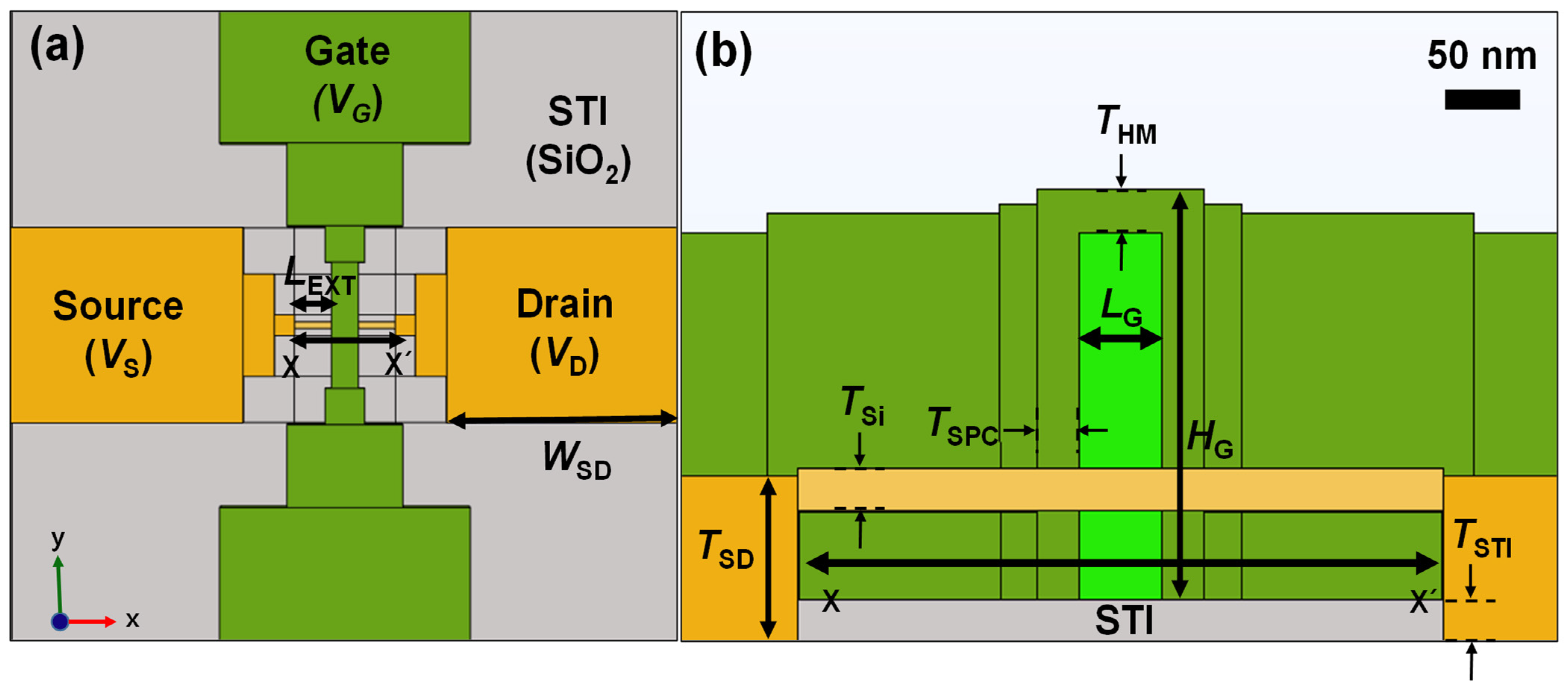
Gate-all-around (GAA) FETs, fabricated on bulk wafer [9], as shown in Figure 1, were simulated as test specimens. The channel thickness (TSi), channel width (WNW), gate length (LG), and gate height (HG) were 20 nm, 20 nm, 60 nm, and 250 nm, respectively. The thickness of the gate hard mask (THM) and gate spacer (TSPC), which are composed of SiO2, were 50 nm and 30 nm, respectively.
Figure 2 shows a schematic of a GAA FET built on a bulk substrate for simulations. The Joule heating model in the heat transfer module of COMSOL was applied for 3D thermal profiling. During the simulation, the environment state and heat transfer coefficient (h) were assumed to be air and 10 W/m2K, respectively. After that, punch-through current [10] was used for ETA instead of forward junction current [11] or gate-to-gate [12] current. Detailed device information used for the simulations are summarized in Table 1.
3. Results and Discussion
Figure 3 shows the measured electrical ID-VG characteristics of the GAA FET. The DC characteristic was measured using a B1500A parameter analyzer at room temperature. After measurement of the initial state (e.g., initial state without stress), HCI stress at VG = 2 V and VD = 4 V was deliberately administered for 2 s. After the stress, degradation in the transconductance SS and VT were observed at 227 mV/dec and 0.65 V, respectively. After that, bias conditions with VG = 0.5 V and VD = 6 V were applied for 100 μs to trigger a punch-through current-based ETA (Table 2). In fact, the current at the pinch-off is independent of VG, and the VG of 0.5 V was just referenced from our previous work [10]. After ETA, the aged-device characteristics with respect to SS and VT recovered by 124 mV/dec and −0.05 V, respectively, compared to the initial state (Table 3). These facts show that both electrons were trapped in the gate dielectric, and physical damage at the SiO2/Si interface was effectively cured by the punch-through current-based ETA.
Figure 4 shows a simulated heat distribution profile during ETA driven by the punch-through current in Figure 2. It shows that most of the heat during ETA was concentrated at the source/drain (S/D) extension where gate heat sink could not affect it. The extracted temperature at the S/D was symmetric [13]. However, considering the self-heating effect of semiconductor devices, the drain temperature was higher than that of the source region [14].
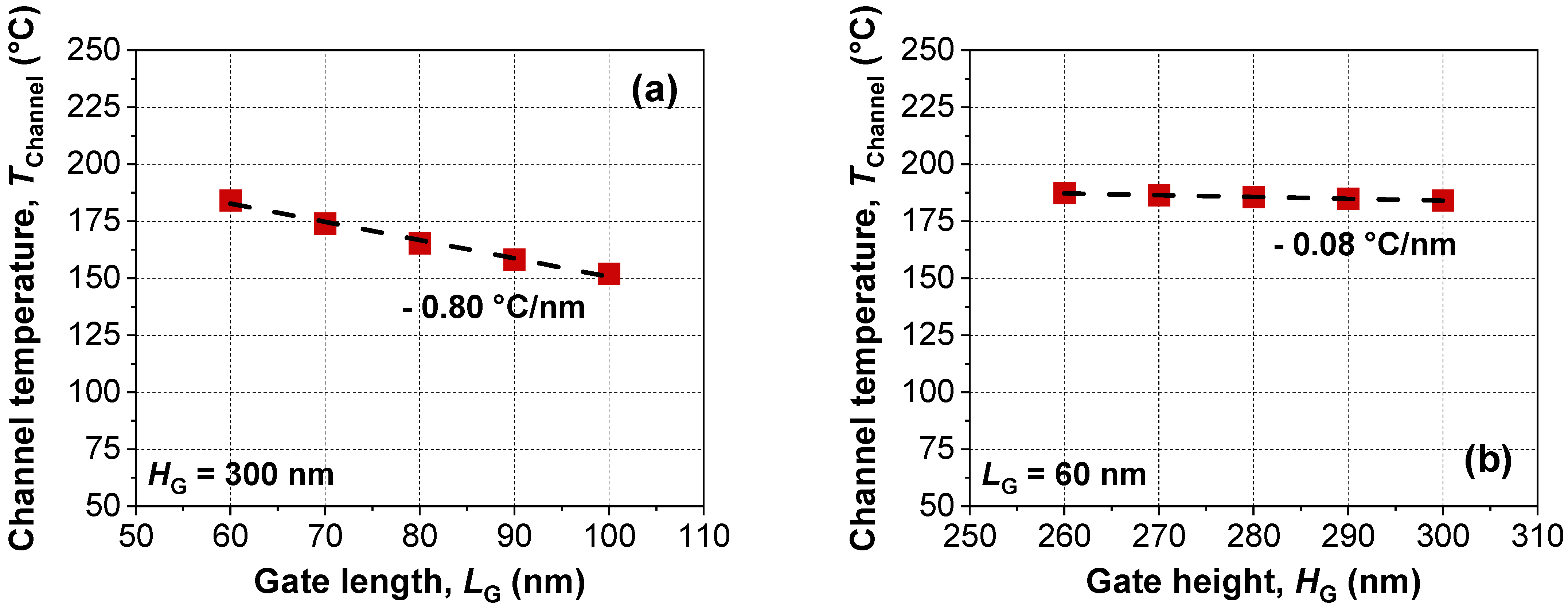
Figure 5 shows the extracted channel temperature (TChannel) with respect to gate electrode scaling. All temperatures were extracted at the center of the silicon nanowire channel, i.e., LG/2.
As the physical gate length and the height of the device were reduced, the temperature during ETA increased. Typically, the gate electrode acts as the heat sink during ETA. As the volume of the gate decreased, the temperature during ETA increased due to the reduced heat sink. The consistent high temperature generated during ETA under identical applied power consumption represented better power efficiency for gate dielectric curing. In this context, considering the extracted sensitivity of temperatures with respect to the gate length and the height, it would be more efficient to apply gate length scaling rather than the gate height. In addition, the gate module includes not only the gate electrode itself but also dielectric materials such as gate dielectric, gate spacer, and gate hard mask.
Figure 6a shows the extracted TChannel with various thicknesses of gate dielectric composed of SiO2. As the gate dielectric thickness (TGD) increased, channel temperature increased under identical power consumption due to decreased heat dissipation through the gate electrode. However, considering the gate dielectric thickness was scaled down for better suppression of SCEs, this approach seems impractical for reducing power consumption. Alternatively, the material engineering shown in Figure 6b would be more efficient. As the thermal conductivity (κ) of the gate dielectric decreased, temperature sensitivity with applied power increased, due to increased thermal isolation, i.e., reduced heat dissipation with low κ.
Figure 7a shows the extracted TChannel with various dielectric thicknesses of gate hard mask (THM) and gate spacer (TSPC). The THM had a negligible effect on TChannel compared with the gate dielectric engineering in Figure 6. As the gate spacer increased, the temperature during ETA decreased due to the increased surface area of the gate spacer. Since convective cooling is performed through the air, a gate spacer with a small width and surface area would be more preferred to lower power consumption. Figure 7b shows the extracted channel temperature with various levels of thermal conductivity for the gate hard mask and the spacer. As the thermal conductivity of the dielectrics decreased, temperature sensitivity increased due to increased thermal isolation.
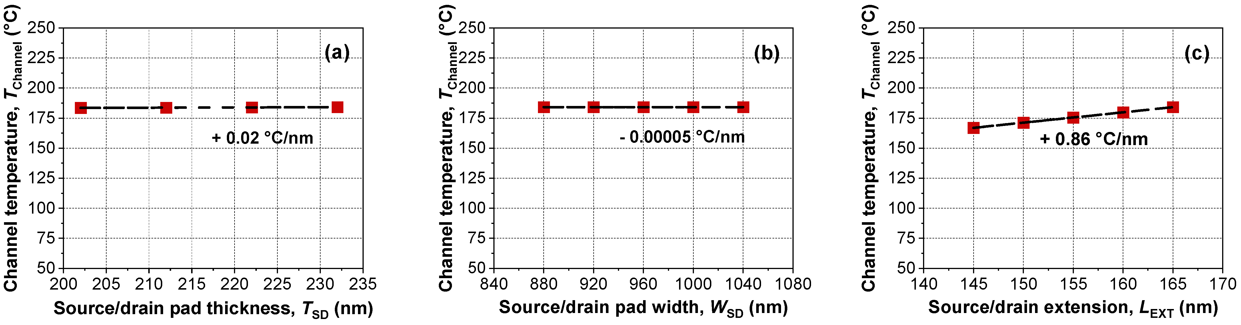
In contrast to the results in Figure 5 to Figure 7, which focused on the gate module, Figure 8 shows the device temperature with respect to modifications of the S/D module. However, even though the S/D extension showed the largest temperature sensitivity (Figure 8c), the sensitivity stemming from S/D was negligible. Moreover, considering the S/D extension (LEXT) had been scaled down for better packing density, this approach seems impractical. In this context, reducing power consumption by engineering of the S/D module is not recommended.
Figure 9a shows the extracted TChannel in the case of the isolation engineering by use of shallow trench isolation (STI) technology. As thickness TSTI increased, channel temperature could be increased due to the increased thermal isolation. However, the change was negligible because the channel was suspended from the STI. Figure 9b shows power efficiency with various buried dielectric materials. When a low thermal conductive material, e.g., HfO2, is employed instead of SiO2, the channel temperature could be increased under identical power consumption. Based on these results, our recommendation to maximize power efficiency is to apply low thermally conductive materials as an STI.
Table 4 provides a summary of the temperature sensitivities for the different geometries and materials of the GAA FET. It can be concluded that the most significant design parameter for determining power efficiency is gate module engineering. As a result, the approach using gate module engineering would be more preferred to reducing power consumption for punch-through current-based ETA.
4. Conclusions
Device guidelines for reducing the power of punch-through current annealing were investigated using 3D COMSOL simulations. Power management efficiency can be improved with dimensional and material engineering. The impacts of device scaling with respect to gate module, source/drain (S/D) module, and isolation, were compared in detail. The gate module engineering was found to be the most significant way to reduce power consumption. However, in contrast to the gate module, impacts of the S/D and shallow trench isolation were negligible.
Author Contributions
J.-Y.P. and Y.-K.C. conceived this project and designed all the experiments. M.-K.K. conducted all the simulations and wrote this paper. All authors have read and agreed to the published version of the manuscript.
Funding
This work was supported by the National Research Foundation (NRF) with a grant funded by the Korea government (MSIT) (No. 2020M3H2A1076786 and 2021R1F1A1049456).
Conflicts of Interest
The authors declare no conflict of interest.
References
- Moroz, V.; Huang, J.; Arghavani, R. Transistor Design for 5 nm and Beyond: Slowing Down Electrons to Speed Up Transistors. In Proceedings of the 17th International Symposium on Quality Electronic Design (ISQED), Santa Clara, CA, USA, 15–16 March 2016; pp. 278–283. [Google Scholar] [CrossRef]
- Ciou, F.-M.; Lin, J.-H.; Chen, P.-H.; Chang, T.-C.; Chang, K.-C.; Hsu, J.-T.; Lin, Y.-S.; Jin, F.-Y.; Hung, W.-C.; Yeh, C.-H.; et al. Comparison of the Hot Carrier Degradation of N- and P-Type Fin Field-Effect Transistors in 14-nm Technology Nodes. IEEE Electron Device Lett. 2021, 42, 1420–1423. [Google Scholar] [CrossRef]
- Lee, K.; Kaczer, B.; Kruv, A.; Gonzalez, M.; Degraeve, R.; Tyaginov, S.; Grill, A.; Wolf, I.D. Hot-Electron-Induced Punch-Through (HEIP) Effect in p-MOSFET Enhanced by Mechanical Stress. IEEE Electron Device Lett. 2021, 42, 1424–1427. [Google Scholar] [CrossRef]
- Hu, C.; Simon, C.T.; Hsu, F.-C.; Ko, P.-K.; Chan, T.-Y.; Terrill, K.W. Hot-Electron-Induced MOSFET Degradation-Model, Monitor, and Improvement. IEEE J. Solid State Circuit 1985, 20, 295–305. [Google Scholar] [CrossRef]
- Takeda, E.; Suzuki, N. An Empirical Model for Device Degradation Due to Hot-Carrier Injection. IEEE Electron Dev. Lett. 1983, 4, 111–113. [Google Scholar] [CrossRef]
- Onishi, K.; Kang, C.S.; Choi, R.; Cho, H.-J.; Gopalan, S.; Nieh, R.E.; Krishnan, S.A.; Lee, J.C. Improvement of Surface Carrier Mobility of Hfo2 Mosfets By High-Temperature Forming Gas Annealing. IEEE Trans. Electron Devices 2003, 50, 384–390. [Google Scholar] [CrossRef]
- Jo, M.; Chang, M.; Park, H.; Hwang, H. Improvement of Hafnium Oxide/Silicon Oxide Gate Dielectric Stack Quality by High Pressure D2O Post Deposition Annealing. Jpn. J. Appl. Phys. 2007, 46, L531–L533. [Google Scholar] [CrossRef]
- Park, J.-Y.; Moon, D.-I.; Lee, G.-B.; Choi, Y.-K. Curing of Aged Gate Dielectric by the Self-Heating Effect in MOSFETs. IEEE Trans. Electron Devices 2020, 67, 777–788. [Google Scholar] [CrossRef]
- Moon, D.-I.; Choi, S.-J.; Kim, C.-J.; Kim, J.-Y.; Lee, J.-S.; Oh, J.-S.; Lee, G.-S.; Park, Y.-C.; Hong, D.-W.; Lee, D.-W.; et al. Silicon Nanowire All-Around Gate Mosfets Built on a Bulk Substrate by All Plasma-Etching Routes. IEEE Electron Device Lett. 2011, 32, 452–454. [Google Scholar] [CrossRef]
- Park, J.-Y.; Hur, J.; Choi, Y.-K. Demonstration of a Curable Nanowire FinFET Using Punchthrough Current to Repair Hot-Carrier Damage. IEEE Electron Dev. Lett. 2018, 39, 180–183. [Google Scholar] [CrossRef]
- Lee, G.-B.; Kim, C.-K.; Park, J.-Y.; Bang, T.; Bae, H.; Kim, S.-Y.; Ryu, S.-W.; Choi, Y.-K. A Novel Technique for Curing Hot-Carrier-Induced Damage by Utilizing the Forward Current of the PN-Junction in a MOSFET. IEEE Electron Dev. Lett. 2017, 38, 1012–1014. [Google Scholar] [CrossRef]
- Moon, D.-I.; Park, J.-Y.; Han, J.-W.; Jeon, G.-J.; Kim, J.-Y.; Moon, J.-B.; Seol, M.-L.; Kim, C.-K.; Lee, H.C.; Meyyappan, M.; et al. Sustainable Electronics for Nano-Spacecraft in Deep Space Missions. In Proceedings of the IEEE International Electron Devices Meeting (IEDM), San Francisco, CA, USA, 3–7 December 2016; pp. 3–7. [Google Scholar] [CrossRef]
- Jeon, C.-H.; Park, J.-Y.; Seol, M.-L.; Moon, D.-I.; Hur, J.; Bae, H.; Jeon, S.-B.; Choi, Y.-K. Joule Heating to Enhance the Performance of a Gate-All-Around Silicon Nanowire Transistor. IEEE Trans. Electron Devices 2016, 63, 2288–2292. [Google Scholar] [CrossRef]
- Pop, E.; Sinha, S.; Goodson, K.E. Heat Generation and Transport in Nanometer-Scale Transistors. Proc. IEEE 2006, 94, 1587–1601. [Google Scholar] [CrossRef]
Figure 1.
Transmission electron microscopy (TEM) image of the fabricated GAA FET.

Figure 2.
Schematic of the device used for simulations. (a) Top-view image of the GAA FET. (b) Cross-sectional image of the GAA FET cut along the x–x′ direction.
Figure 2.
Schematic of the device used for simulations. (a) Top-view image of the GAA FET. (b) Cross-sectional image of the GAA FET cut along the x–x′ direction.

Figure 3.
Measured ID-VG characteristic of the fabricated n-channel GAA FET.

Figure 4.
(a) Simulated heat distribution division profile during punch-through-based ETA under bias conditions with VG = 0.5 V, VS. = 0 V, and VD = 6 V. (b) Extracted temperature of the device along the x–x′ direction during ETA.
Figure 4.
(a) Simulated heat distribution division profile during punch-through-based ETA under bias conditions with VG = 0.5 V, VS. = 0 V, and VD = 6 V. (b) Extracted temperature of the device along the x–x′ direction during ETA.

Figure 5.
Extracted TChannel of devices with various (a) gate lengths and (b) gate heights under an identical power consumption of 0.45 mW. Dashed lines indicate linear fits of the experimental data.
Figure 5.
Extracted TChannel of devices with various (a) gate lengths and (b) gate heights under an identical power consumption of 0.45 mW. Dashed lines indicate linear fits of the experimental data.

Figure 6.
Extracted TChannel of devices with various (a) thicknesses and (b) materials of gate dielectric. Dashed lines indicate linear fits of the experimental data.
Figure 6.
Extracted TChannel of devices with various (a) thicknesses and (b) materials of gate dielectric. Dashed lines indicate linear fits of the experimental data.

Figure 7.
Extracted TChannel of devices with various (a) dielectric thicknesses and (b) materials of gate hard mask and gate spacer. Dashed lines indicate fitting of the symbols.
Figure 7.
Extracted TChannel of devices with various (a) dielectric thicknesses and (b) materials of gate hard mask and gate spacer. Dashed lines indicate fitting of the symbols.

Figure 8.
Extracted TChannel of devices with various (a) S/D pad thicknesses, (b) S/D pad widths, and (b,c) S/D extension lengths. Dashed lines indicate linear fits of the experimental data.
Figure 8.
Extracted TChannel of devices with various (a) S/D pad thicknesses, (b) S/D pad widths, and (b,c) S/D extension lengths. Dashed lines indicate linear fits of the experimental data.

Figure 9.
Extracted TChannel of devices with various (a) thickness and (b) materials of shallow trench isolation (STI). Dashed lines indicate linear fits of the experimental data.
Figure 9.
Extracted TChannel of devices with various (a) thickness and (b) materials of shallow trench isolation (STI). Dashed lines indicate linear fits of the experimental data.


Table 1.
Dimensional and material parameters for COMSOL simulations.
| Geometry | Dimension | Material | Thermal Conductivity [W/m∙K] |
|---|---|---|---|
| Gate length, LG [nm] | 60 | Poly-Si | 31.2 |
| Gate height, HG [nm] | 300 | ||
| Gate hard mask thickness, THM [nm] | 30 | SiO2 | 1 |
| Gate spacer thickness, TSPC [nm] | 30 | ||
| Gate dielectric thickness, TGD [nm] | 5 | ||
| STI thickness, TSTI [nm] | 70 | ||
| Source/drain pad thickness, TSD [nm] | 232 | Si | 149 |
| Source/drain pad width, WSD [nm] | 1040 | ||
| Channel thickness, TSi [nm] | 20 | ||
| Channel width, WNW [nm] | 20 | ||
| Source/drain extension length, LEXT [nm] | 165 |
Table 2.
Bias conditions for punch-through current based ETA.
| Bias Condition | |
|---|---|
| Gate voltage (VG) | 0.5 V |
| Source voltage (VS) | 0 V |
| Drain voltage (VD) | 6 V |
| Punch-through current (IPunch) | 75 μA |
| Power consumption, (P = VD × IPunch) | 0.45 mW |
| Annealing time (t) | 100 μs |
Table 3.
Extracted device parameters before HCI, after HCI and ETA.
| Initial State (Before HCI) | After HCI | After Punch-Through ETA | |
|---|---|---|---|
| SS (mV/dec) | 82 mV/dec | 227 mV/dec | 124 mV/dec |
| VT (V) | −0.13 V | 0.65 V | −0.05 V |
Table 4.
Summary of temperature sensitivity according to dimensional and material engineering of the gate, S/D, and isolation module for the punch-through current-based local thermal annealing.
Table 4.
Summary of temperature sensitivity according to dimensional and material engineering of the gate, S/D, and isolation module for the punch-through current-based local thermal annealing.
| Gate Module | S/D Module | Isolation | |
|---|---|---|---|
| Minimum (°C/nm) | −0.80 | 0.00 | +0.05 |
| Maximum (°C/nm) | +3.70 | +0.86 |
Publisher’s Note: MDPI stays neutral with regard to jurisdictional claims in published maps and institutional affiliations. |
© 2022 by the authors. Licensee MDPI, Basel, Switzerland. This article is an open access article distributed under the terms and conditions of the Creative Commons Attribution (CC BY) license (https://creativecommons.org/licenses/by/4.0/).
Share and Cite
MDPI and ACS Style
Kim, M.-K.; Choi, Y.-K.; Park, J.-Y. Power Reduction in Punch-Through Current-Based Electro-Thermal Annealing in Gate-All-Around FETs. Micromachines 2022, 13, 124. https://0-doi-org.brum.beds.ac.uk/10.3390/mi13010124
AMA Style
Kim M-K, Choi Y-K, Park J-Y. Power Reduction in Punch-Through Current-Based Electro-Thermal Annealing in Gate-All-Around FETs. Micromachines. 2022; 13(1):124. https://0-doi-org.brum.beds.ac.uk/10.3390/mi13010124
Chicago/Turabian StyleKim, Min-Kyeong, Yang-Kyu Choi, and Jun-Young Park. 2022. "Power Reduction in Punch-Through Current-Based Electro-Thermal Annealing in Gate-All-Around FETs" Micromachines 13, no. 1: 124. https://0-doi-org.brum.beds.ac.uk/10.3390/mi13010124
Note that from the first issue of 2016, this journal uses article numbers instead of page numbers. See further details here.