A Thermal Tuning Meta-Duplex-Lens (MDL): Design and Characterization
by
 , , and
Ning Xu
1, 
Yaoyao Liang
2,
Yuan Hao
1,
Min Mao
1,
Jianping Guo
1,
Hongzhan Liu
1,
Hongyun Meng
1 ,
,
Faqiang Wang
1 and
Zhongchao Wei
1,*
1
Guangdong Provincial Key Laboratory of Nanophotonic Functional Materials and Devices, School of Information and Optoelectronic Science and Engineering, South China Normal University, Guangzhou 510006, China
2
Centre de Nanosciences et de Nanotechnologies, CNRS, Université Paris-Sud—Université Paris-Saclay 10 Boulevard Thomas Gobert, 91120 Palaiseau, France
*
Author to whom correspondence should be addressed.
Nanomaterials 2020, 10(6), 1135; https://0-doi-org.brum.beds.ac.uk/10.3390/nano10061135
Submission received: 29 April 2020
/
Revised: 1 June 2020
/
Accepted: 6 June 2020
/
Published: 8 June 2020
(This article belongs to the Special Issue Photonic Nanomaterials)
Abstract
:Multifunctional metasurfaces play an important role in the development of integrated optical paths. However, some of the realizations of current multifunctional metasurface devices depend on polarization selectivity, and others change the polarization state of the outgoing light. Here, based on vanadium dioxide (VO2) phase change material, a strategy to design a meta-duplex-lens (MDL) is proposed and numerical simulation calculations demonstrate that at low temperature (about 300 K), VO2 behaves as a dielectric so that the MDL can act as a transmission lens (transmission efficiency of 87.6%). Conversely, when VO2 enters the metallic state (about 355 K), the MDL has the ability to reflect and polymerize electromagnetic waves and works as a reflection lens (reflection efficiency of 85.1%). The dielectric waveguide and gap-surface plasmon (GSP) theories are used in transmission and reflection directions, respectively. In order to satisfy the coverage of the phase gradient in the range of 2π in both cases, we set the antenna as a nanopillar with a high aspect ratio. It is notable that, via symmetrical antennas acting in concert with VO2 phase change material, the polarization states of both the incident light and the outgoing light are not changed. This reversible tuning will play a significant role in the fields of imaging, optical storage devices, communication, sensors, etc.
1. Introduction
A metasurface [1,2], an artificial composite material with equivalent constitutive parameters synthesized by sub-wavelength structures, exhibits a strong ability to manipulate electromagnetic waves. Compared with traditional optics device, metasurface devices are free of bulky volume and complicated optical path design. The advantages of simple manufacturing, powerful function and easy integration are essential for developing the next generation of integrated optical circuits. There are plenty of theories studying spatial gradient metasurfaces, including but not limited to the theories of dielectric waveguide [3,4], Pancharatnam–Berry phase [5], photonic spin Hall effect (PSHE) [6,7], gap-surface plasmon (GSP) [8,9,10], etc. According to these theories, a number of promising metasurface applications have been proposed, such as metalenses [3,11,12,13], perfect absorbers [14,15], polarization converters [16], and vortex generators [17]. With the deepening of research, single functional metasurfaces have been replaced by versatile and even tunable metasurfaces, which can be realized by utilizing the microelectromechanical system (MEMS) [18], stretchable substrate metasurface [19,20], phase change materials (Ge2Se2Te5 [21,22,23], VO2 [24,25,26]), liquid crystal [27] or graphene [28,29,30]. As a thermally sensitive phase change material, VO2 is of great function for the reversible phase change in both insulating and metallic states. Exploiting the insulator-metal transition characteristics of VO2, lots of novel devices have been proposed, including VO2-based absorbers [31,32], tunable-focusing lenses [33], absorber-lenses [34,35], and perfect absorber and polarization converter bifunctional devices [36]. However, part of the multifunctional metasurfaces are implemented by changing the polarization state of the incident light, while the others change the polarization state of outgoing light. The application of multifunctional metasurfaces are restricted by these problems in practical applications.
In this paper, based on VO2 phase change material, a general strategy to design a thermal tuning meta-duplex-lens (MDL) in the mid-infrared range (4 µM) is proposed and numerical simulation calculation demonstrated by commercial software FDTD Solutions (Lumerical Inc. in Vancouver, BC, Canada). The designed meta-atoms have the property of realizing transmission and reflection by controlling their temperature. Therefore, in the same structure, transmission or reflection optical focusing can be achieved respectively. At low temperature (about 300 K), VO2 enters the insulated state (hereinafter referred to as VO2-I). It behaves as a dielectric such that the MDL can deflect and converge electromagnetic waves (transmission efficiency of 87.6%). Conversely, when VO2 goes into the metallic state (about 355 K) (hereinafter referred to as VO2-M), the MDL could reflect and polymerize electromagnetic waves (reflection efficiency of 85.1%). To achieve this strategy, we use the dielectric waveguide and gap-surface plasmon (GSP) theories in transmission and reflection modes, respectively. In order to satisfy the coverage of the phase gradient in the range of 2π in both cases, we set the antenna as a nanopillar with a high aspect ratio. The innovations of our research are mainly demonstrated in two aspects. One is that, via symmetrical antennas act in concert with VO2 phase change material, we do not change the structures of the MDL and the polarization state of the incident light and have no effect on the polarization state of the outgoing light. The other is that, in the same structure, without changing the structural parameters, the active surface temperature control of the metasurface realizes duplex focusing. This device will play an important role in the fields of integrated optical circuit, sensors, optical storage devices, and biological imaging.
2. Materials and Methods
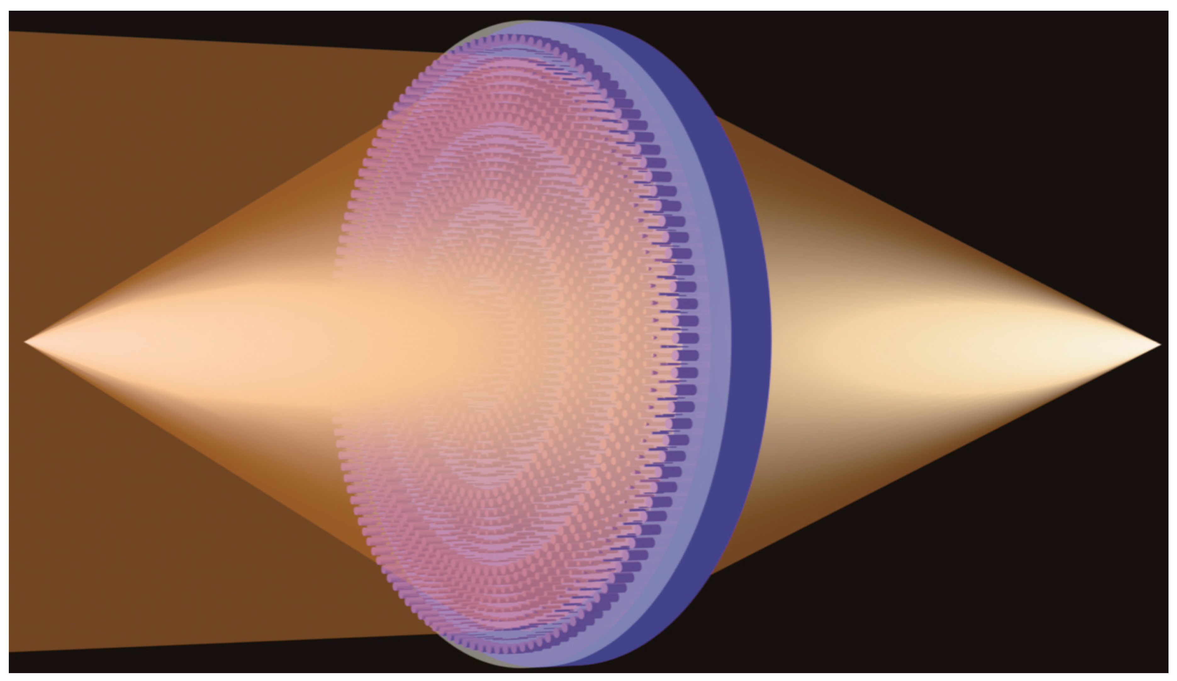
Figure 1 shows the working schematic of a designed device. At room temperature (300 K), the metalens works in transmission mode to focus the incident beam (left). When the temperature rises to 355 K, the metalens works as a reflection metalens (right). It accomplishes the phase modulation in the whole space, which breaks the limitation of the previous metasurfaces that can only operate in half the space. Besides that, it has the property of polarization independence and does not change the polarization state of the outgoing beam.
The essence of the MDL is to design the meta-atoms which could be controlled by temperature to achieve transmission or reflection. These meta-atoms are then combined to cover the phase gradient in whole 2π range. For the purpose, we use the dielectric waveguide and gap-surface plasmon (GSP) theories in transmission and reflection modes, respectively. The application of this design allows our MDL to achieve phase modulation in two directions. In order to satisfy the coverage of the phase gradient in the range of 2π in both cases, we set the antenna as a metal-like nanopillar with high aspect ratio [37]. Since the designed nanopillar antennas are periodically symmetrical, it can achieve polarization-independent focusing in two modes. Therefore, the mode switching is only related to the phase transition state.
2.1. Material Model Analysis
VO2 has received widespread attention due to its special property of reversible phase change from insulator to metal. The complex permittivity is given by the following well-known dispersion relation [38,39]:
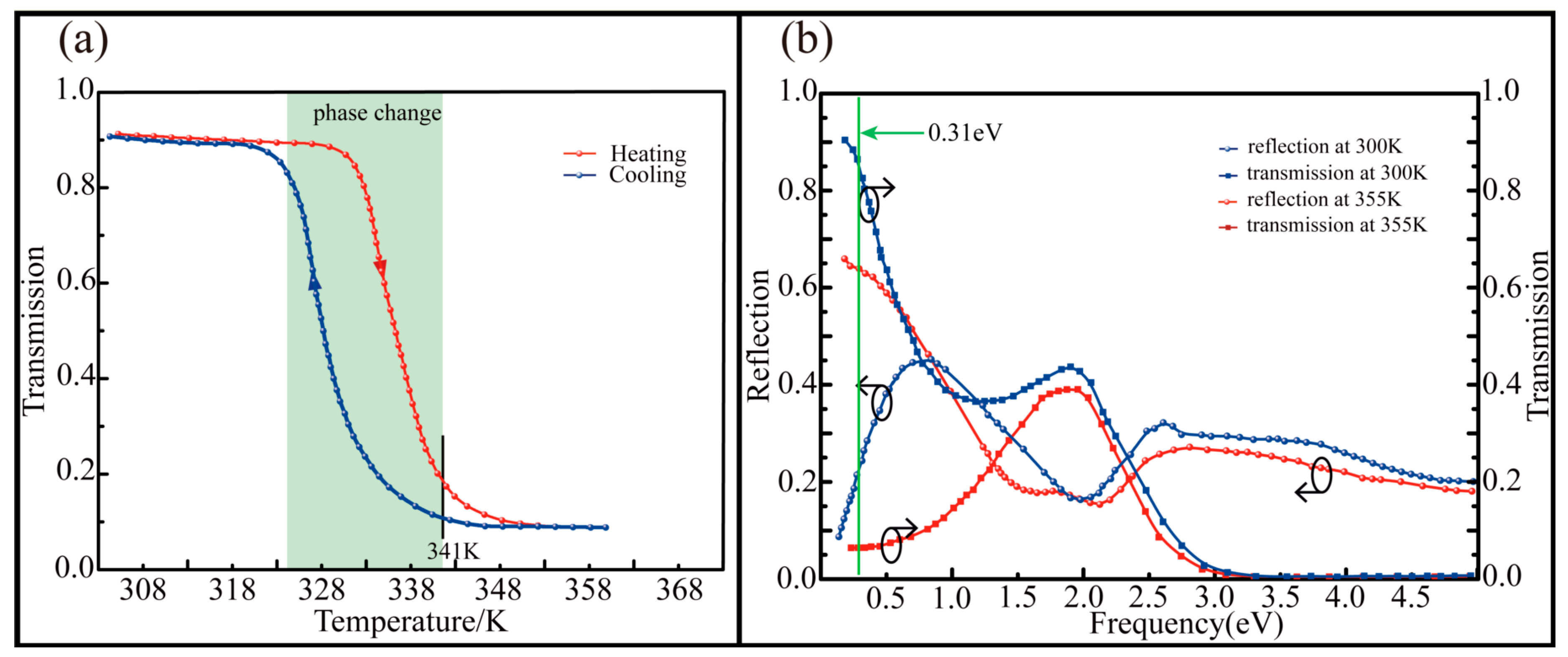
The first term is ultimate high frequency permittivity of VO2 material. The second term stands for the contribution of free electron to the dielectric constant. In this term, is the carrier density, which is related to the plasma frequency, and is the collision frequency, where is the number of conduction electrons and is the optical quality of electrons. The summation of Lorentz or classical vibrators is provided by the third term, which considers the non-constant contribution to the remaining dielectric constant within the spectral region of interest. In this term, the lattice vibration intensity, frequency and linewidth are represented by , , and , respectively. The optical properties of VO2 film are demonstrated in Figure 2 [39]. Figure 2a depicts the temperature dependence of optical transmission of VO2 film at 4 µM. With the increase of temperature, some of the molecules in VO2 undergo phase change and diffusion and form a metallic phase structure. The VO2 material changes from insulating state to metallic state and the ratio of transmission decreases accordingly. When the critical temperature reaches 341 K, the phase transition is completed. Conversely, the increasing of transmission is caused by the decreasing of temperature, which indicates that the temperature phase transition of VO2 is a reversible process. The bi-phase transmission and reflection spectra at 0.25–5 eV (0.248–4.96 µM) are shown in Figure 2b. It is obvious that VO2 has a high optical transparency and contrast in the infrared band so that we choose to design and simulate the metasurface at the frequency of 0.31 eV (4 µM).
2.2. Dielectric Waveguide Theory
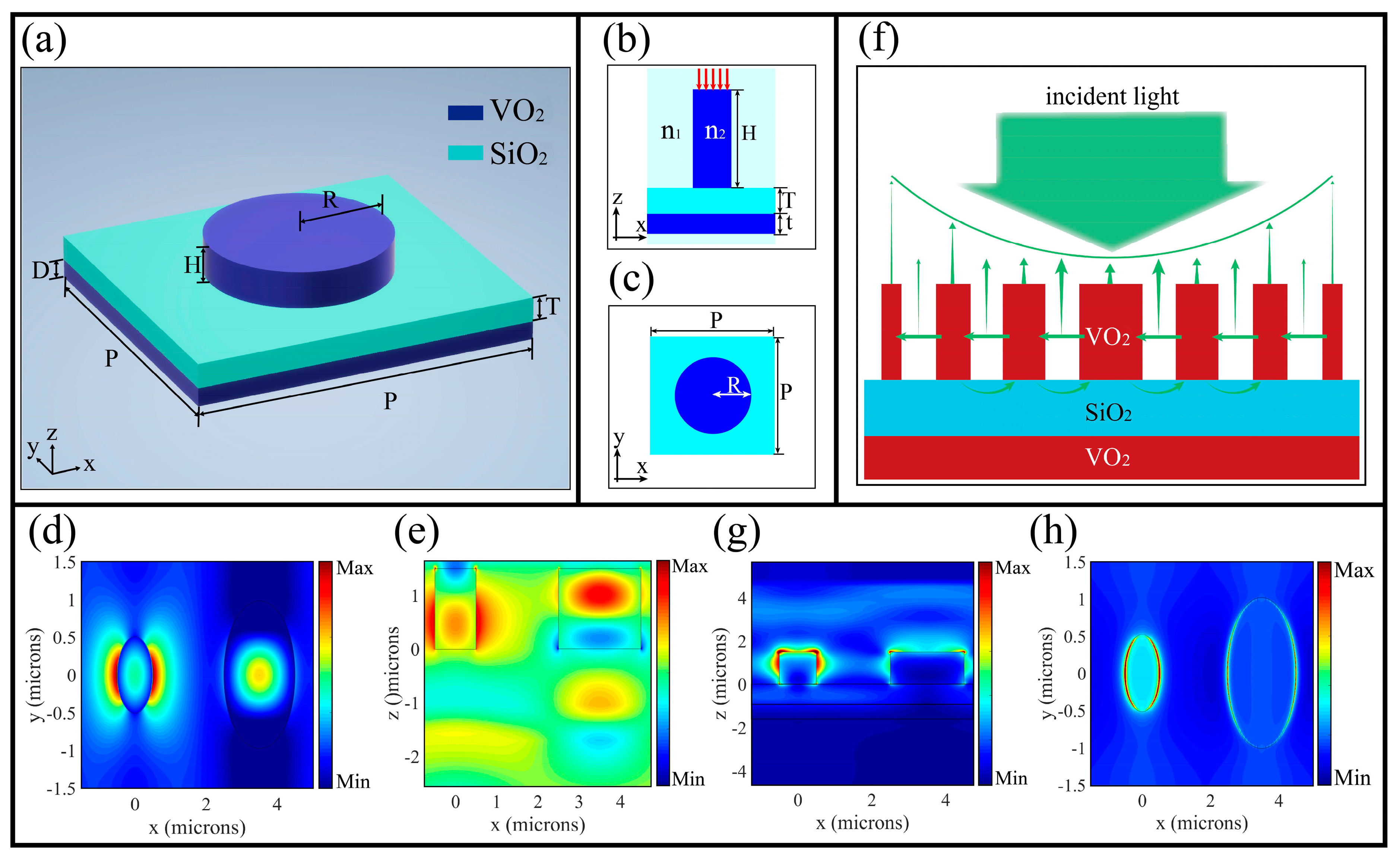
Figure 3a–c illustrate the meta-atoms of the designed metasurface. The unit size of the meta-atom is optimized by parameter sweeps, which is obtained H = 1.5 µM, T = 1 µM, D = 0.7 µM. The lattice constant p is chosen to be 3.5 µM to avoid coupling of adjacent waveguides. At room temperature (about 300 K), VO2-I is a normal dielectric material with high refractive index (n~3) so that it can form an all-dielectric transmission array metasurface. The phase imparted solely by the waveguiding effect is given by [40]:
where is the effective index of the fundamental mode () and H (nanocolumns height) is the propagation length. The can be readily computed by a single step-index circular waveguide model. The electric near field distribution in xy-plane and xz-plane are illustrated in Figure 3d,e. Left and right pillars have radius of 0.5 µM and 1 µM, respectively. Most of the electromagnetic wave is trapped in the nano-pillar and unit cell period is optimized to ensure that near-field coupling does not occur in adjacent waveguides.
2.3. Gap Surface Plasmon Waveguide Theory
Accompanying with the rise in temperature, VO2-M on both sides of the substrate enter the metallic phase to form a metal-insulator-metal (MIM) structure, which composes a metasurface of the reflective array. The schematic diagram is given in Figure 3f. Different from previous metal patches, we apply metal nanocolumns (the height is on the order of microns) to a reflection metasurface for the first time. Due to the fact that high nanocolumns can be equivalent to waveguides, GSP resonance is formed between the two adjacent nanocolumns. Therefore, two adjacent VO2 nanopillars and air can be treated as a traditional MIM structure [41]. The surface plasma wave is excited by the evanescent wave at the boundary of the waveguide and the electric field in the waveguide is coupled with the surface plasma wave. The dispersion relation of an MIM obeys the following dispersion equation [42]:
where and are the dielectric constants of the insulator and the metal. d is the width of the inner insulator. and are the longitudinal propagation constants in the insulator and metal, respectively. They are related to the effective index of refraction as:
where is the wave number in a vacuum. Figure 3g,h illustrates the electric field distribution in the xy-plane and xz-plane. Left and right pillars also have the radius of 0.5 µM and 1 µM, respectively. In this paper, the dielectric layer is equivalent to air. The propagation of light is controlled by changing the spacing between the two nanocolumns, which is equivalent to changing the spacing d.
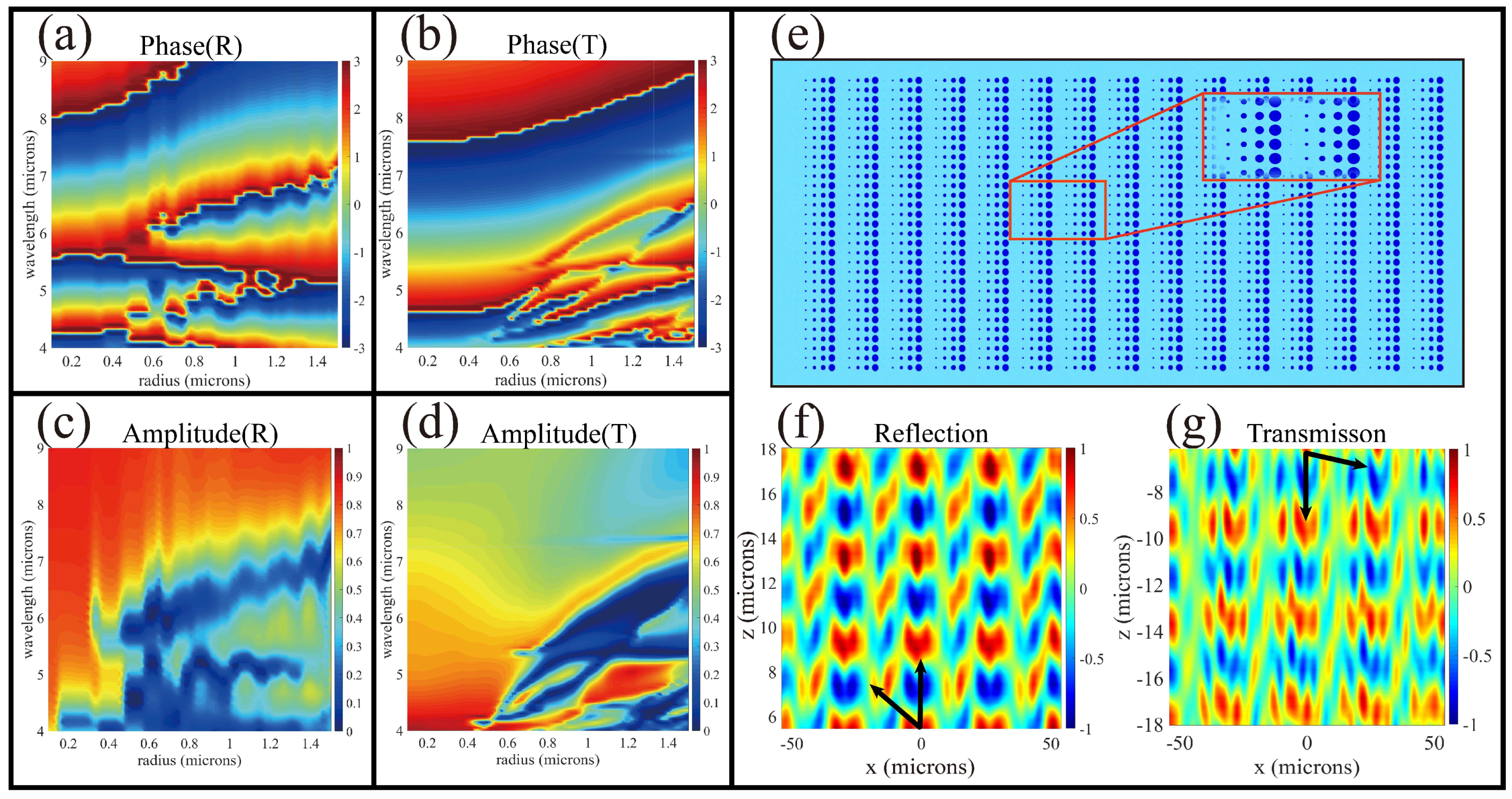
Figure 4a–d stand for the dependency of utilizing finite difference time domain (FDTD) numerical simulation with phase shift, transmission and reflection on the incidence wavelength. The cylinder cross-section radius are investigated based on commercial software FDTD Solutions (Lumerical Inc., Vancouver, BC, Canada). The radius varies from 0.1 µM to 1.5 µM in steps of 20 nm and the wavelength varies from 4 µM to 9 µM with intervals of 70 nm. Although the phase change state of VO2 is switched so that the phase regulated by each antenna is different, the overall trend is roughly consistent with the phase profile of the hyperbolic super lens. Therefore, duplex focusing can be achieved without changing the structure. In order to prove the MDL deflection function to the beam, we first design the metasurface as shown in Figure 4e. According to the generalized Snell’s laws of reflection and refraction [43], the reflection angle and refraction angle can be calculated using:
where is the incidence angle, is the working wavelength and is the imposed boundary phase discontinuity. Figure 4f,g depicts the electric fields distribution of the transmission and reflection. When the metasurface works in transmission mode (300 K), the device realizes the refraction function. With the temperature increases (355 K), the device enters a reflective state, which accords with the theoretical values quite well. Different from the simulation of one-to-two-period nanopillar arrays that are usually arranged manually with FDTD, this article adopts multiple period antennae and uses generalized Snell’s law to automatically place nanopillars with appropriate radius through scripts. Therefore, the obtained electric field is illustrated in Figure 4f,g and the deflected electric fields of multiple cycles are alternately arranged.
3. Concept and Design of Meta-Duplex-Lenses
3.1. Design of MDL
The components of the metalens are the VO2 nanocolumns on the glass substrate (SiO2) and the VO2 layer below. In order to achieve focus, each nanopillar in position must meet with the requirement of phases below:
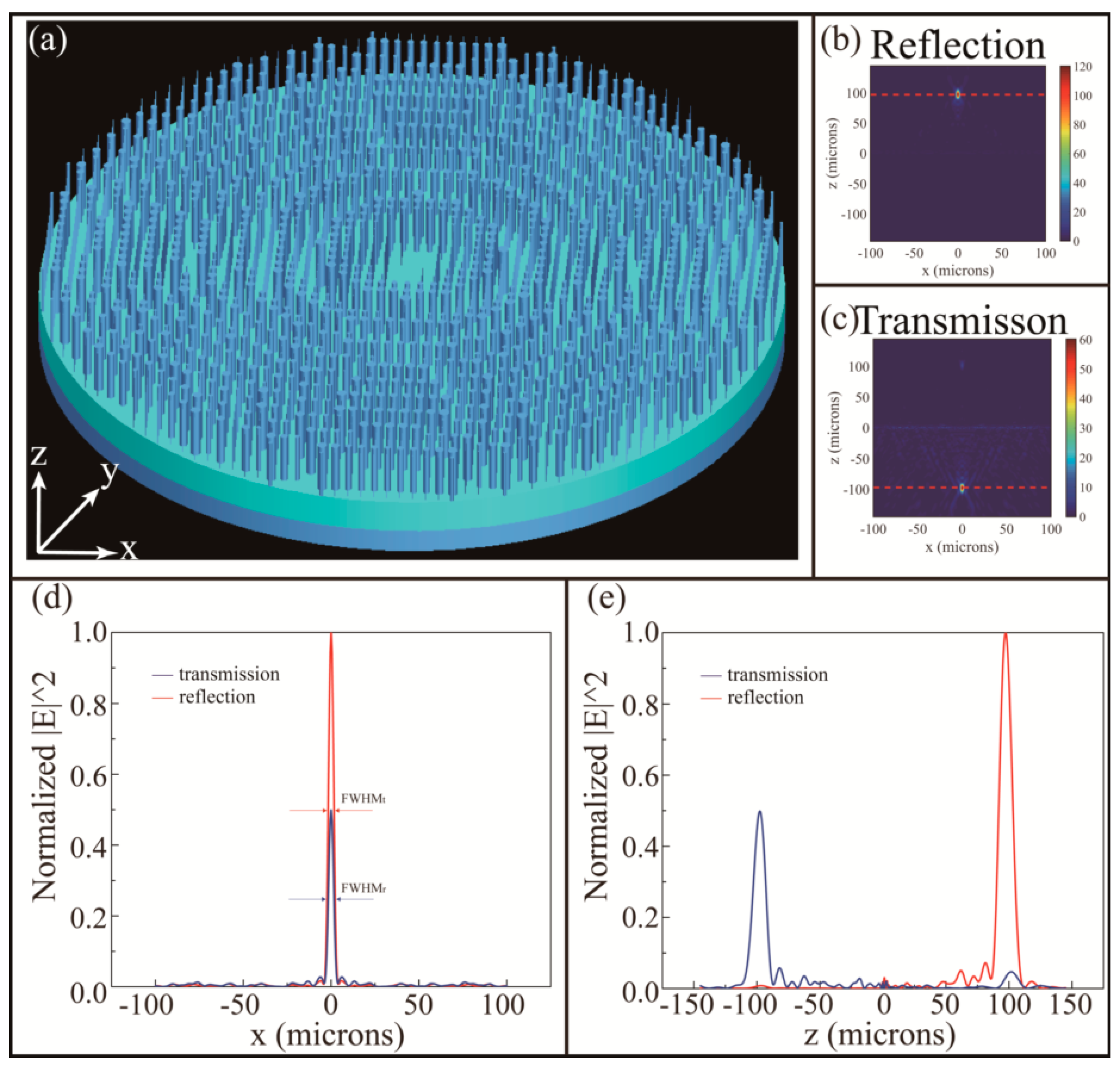
where and denote the center coordinates of the unit located in the x-axis ith row and y-axis jth column, respectively. f is the focal length. is the operation wavelength of 4 µM and n is an arbitrary integer. According to the phase distribution formula given by Equation (7), we design a large-size two-dimensional plane lens. The nanopillar arrangement is displayed in Figure 5a, which has a diameter of 200 µM and an operating wavelength of 4 µM. The parallel light is incident downward along the z-axis and the polarization state is linearly polarized light in the x direction. We assume the positive direction is pointing up along the z-axis. Both in reflection mode and transmission mode, the designed focal length is 100 µM. With the formula , we can calculate the numerical aperture as 0.707.
The far field detection can obtain the electric field strength of the transmission plane (xz-plane) as shown in Figure 5b,c so that the MDL is more intuitively displayed. Among them, the red dotted lines is the focus position. Figure 5d,e indicates the normalized electric field intensity distribution in transmission plane of x = 0 and focal plane of y = 0, respectively. In both figures, the blue line indicates transmission and the red line indicates reflection. The intensity of the focusing in the transmission mode is attenuated (about 50%) comparing to reflective focusing due to the loss of electromagnetic wave propagation in the three-layer medium. The full width at half maximum (FWHM) in the two working states is calculated from the Figure 5e and indicated by the arrow. The FWHM in transmission mode and reflection mode are 3.286 µM and 3.406 µM, respectively. They are both less than 4 µM in wavelength, which enables the lens to achieve sub-wavelength resolution.
3.2. Characterization of Aberration
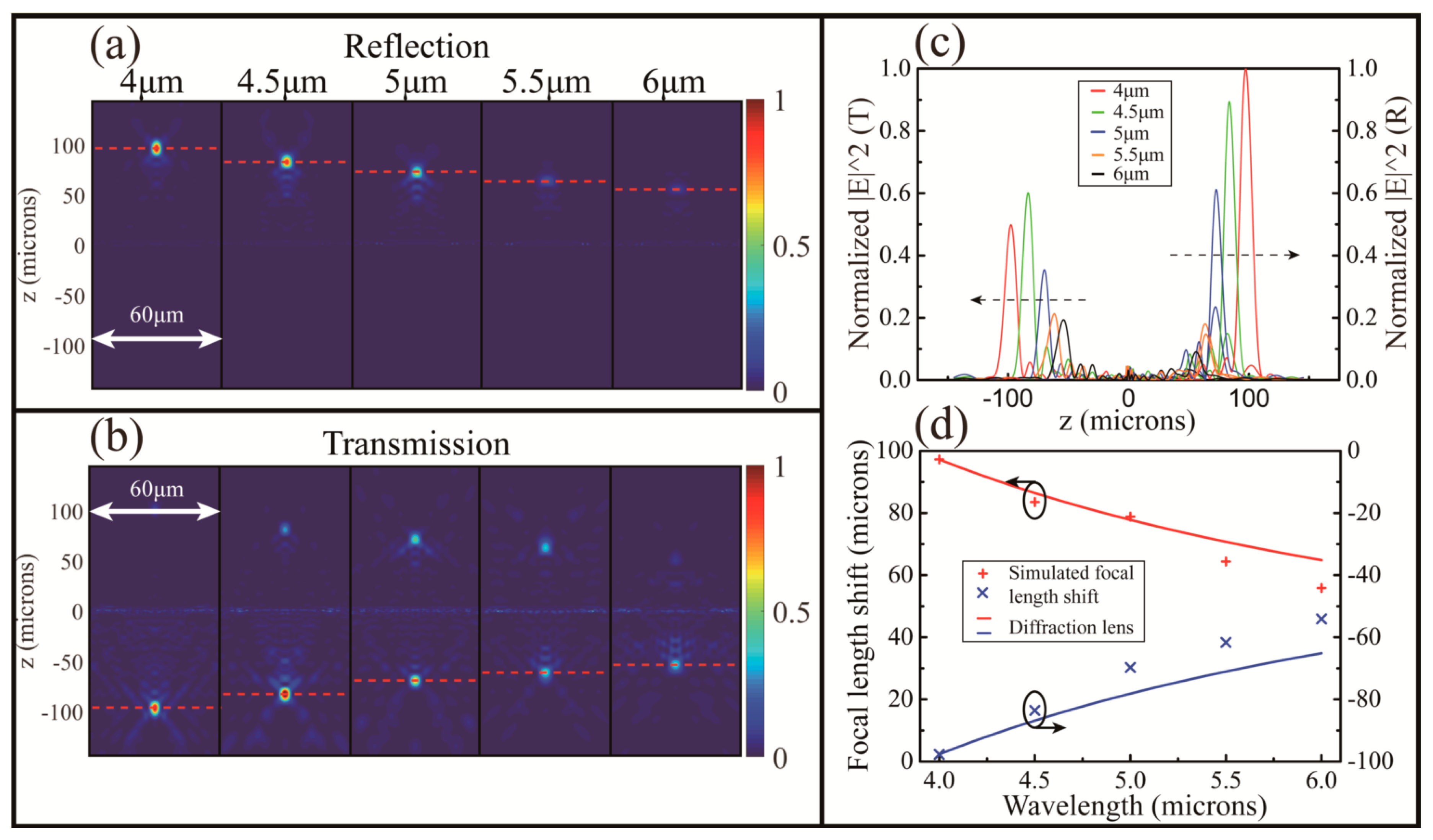
The metalens above is designed to shape the phase profile for a specific wavelength. In order to characterize the lens performance, it is necessary to study the focuses deviation behaviour of the incident light with a different designed wavelength. We select five wavelengths ranging from 4–6 µM for simulation. These normalized electric field intensities of reflection and transmission in the xz-plane are described in Figure 6a,b, respectively.
Here, the focal shift of the diffractive lens is given by:
where is the incident wavelength, and and are the design wavelength and focal length, respectively. Figure 6c is the intensities distribution (in different colors corresponding to their respective wavelengths) of two modes in the xz-plane (y = 0) at different wavelengths ranging from 4 µM to 6 µM, respectively. All intensities are normalized to the intensities of the design wavelength of reflection mode. Intuitively, the focus intensity tends to decrease as it deviates from the design wavelength. The focal lengths decrease when using a wavelength different to its design value for the MDL (Figure 6d).
We calculate the full width at half maximum in the y direction (x = 0) on the focal plane in reflection and transmission. The FWHM in transmission mode and reflection mode are 3.999 µM and 3.707 µM, respectively. In order to fully evaluate the performance of the lens, we also analyzed the astigmatism of the lens. The difference in full width at half maximum in the x and y directions are compared. In reflection, the difference is 0.301 µM, and in transmission, it is 0.713 µM. It can be seen that the imaging quality in reflection mode is better than that in transmission mode, which corresponds to the results obtained in Figure 5 and Figure 6.
In general, transmission efficiency is defined as a ratio of optical power at the focal region on the focal plane to a power of incident light. The power of incident light is equal to the power of light through the aperture of the same size as the lens. Therefore, we can calculate the efficiency in working wavelength are 87.6% (transmission) and 85.1% (reflection), respectively.
4. Conclusions
In conclusion, a strategy of designing a thermal tuning meta-duplex-lens (MDL) is presented in this paper. The designed MDL is capable of achieving the duplex focusing of transmission and reflection. The efficiency is 87.6% (transmission) and 85.1% (reflection), respectively. The main difference from previous jobs is that, using VO2 phase change material, we do not change the structure and the polarization state of the incident light and have no effect on the polarization state of the outgoing light. The dielectric waveguide and gap-surface plasmon (GSP) theories are used in the forward direction and backward direction, respectively. In order to satisfy the coverage of the phase gradient in the range of 2π in both cases, we set the antenna as a nanopillar with a high aspect ratio, which is the first time to apply metal-like nanopillars in reflection metasurfaces. By adjusting the ambient temperature, the phase change of VO2 can be controlled and, consequently, the switching of transmissive and reflective focusing of MDL can be achieved. The phase change of VO2 can be induced by a high energy laser, so the MDL that we proposed can be used as a protectable laser lens. When the incident laser energy exceeds the threshold, the transmission light is reflected into the protectable light path so that the device focused by the laser will not be destroyed. Due to the characteristics of duplex transmission and active temperature tuning of MDL, bidirectional optical storage can be realized, increasing the density of optical storage. This reversible tuning device will play a huge role in the field of integrated optical circuit, optical storage devices, sensors and biological imaging.
Author Contributions
Conceptualization, N.X.; methodology, N.X.; software, N.X.; validation, N.X. and Z.W.; formal analysis, Z.W., J.G., F.W., H.M., H.L., Y.L., Y.H. and M.M.; investigation, N.X. and Z.W.; data curation, M.M.; writing—original draft preparation, M.M.; writing—review and editing, Z.W., J.G., F.W., H.M., H.L., Y.L., Y.H. and M.M.; visualization, N.X.; supervision, Z.W.; project administration, Z.W.; and funding acquisition, Z.W., F.W., H.M. and H.L. All authors have read and agreed to the published version of the manuscript.
Funding
This work was supported by the National Natural Science Foundation of China (NSFC) under Grant Nos. 61774062, 11674109, 61875057, 61475049, 11674107 and Innovation Project of Graduate School of South China Normal University: 2019LKXM026.
Acknowledgments
This work was supported by the National Natural Science Foundation of China (NSFC) and Innovation Project of Graduate School of South China Normal University.
Conflicts of Interest
The authors declare no conflict of interest.
References
- Hsiao, H.-H.; Chu, C.H.; Tsai, D.P. Fundamentals and Applications of Metasurfaces. Small Methods 2017, 1, 1600064. [Google Scholar] [CrossRef] [Green Version]
- Leitis, A.; Heßler, A.; Wahl, S.; Wuttig, M.; Taubner, T.; Tittl, A.; Altug, H. All-Dielectric Programmable Huygens’ Metasurfaces. Adv. Funcl. Mater. 2020, 30, 1910259. [Google Scholar] [CrossRef]
- Liang, Y.; Wei, Z.; Guo, J.; Wang, F.; Meng, H.; Liu, H. Metalenses Based on Symmetric Slab Waveguide and c-TiO2: Efficient Polarization-Insensitive Focusing at Visible Wavelengths. Nanomaterals 2018, 8, 699. [Google Scholar] [CrossRef] [PubMed] [Green Version]
- Khorasaninejad, M.; Capasso, F. Broadband Multifunctional Efficient Meta-Gratings Based on Dielectric Waveguide Phase Shifters. Nano Lett. 2015, 15, 6709–6715. [Google Scholar] [CrossRef] [PubMed]
- Tymchenko, M.; Gomez-Diaz, J.S.; Lee, J.; Nookala, N.; Belkin, M.A.; Alù, A. Gradient Nonlinear Pancharatnam-Berry Metasurfaces. Phy. Rev. Lett. 2015, 115, 207403. [Google Scholar] [CrossRef] [PubMed] [Green Version]
- Yin, X.; Ye, Z.; Rho, J.; Wang, Y.; Zhang, X. Photonic Spin Hall Effect at Metasurfaces. Science 2013, 339, 1405. [Google Scholar] [CrossRef] [Green Version]
- Liu, Y.; Ke, Y.; Luo, H.; Wen, S. Photonic spin Hall effect in metasurfaces: A brief review. Nanophotonics 2017, 6, 51–70. [Google Scholar] [CrossRef]
- Miyata, M.; Hatada, H.; Takahara, J. Full-Color Subwavelength Printing with Gap-Plasmonic Optical Antennas. Nano Lett. 2016, 16, 3166–3172. [Google Scholar] [CrossRef]
- Miyata, M.; Holsteen, A.; Nagasaki, Y.; Brongersma, M.L.; Takahara, J. Gap Plasmon Resonance in a Suspended Plasmonic Nanowire Coupled to a Metallic Substrate. Nano Lett. 2015, 15, 5609–5616. [Google Scholar] [CrossRef]
- Heiden, J.T.; Ding, F.; Linnet, J.; Yang, Y.; Beermann, J.; Bozhevolnyi, S.I. Gap-Surface Plasmon Metasurfaces for Broadband Circular-to-Linear Polarization Conversion and Vector Vortex Beam Generation. Adv. Opt. Mater. 2019, 7, 1801414. [Google Scholar] [CrossRef]
- Khorasaninejad, M.; Chen, W.T.; Devlin, R.C.; Oh, J.; Zhu, A.Y.; Capasso, F. Metalenses at visible wavelengths: Diffraction-limited focusing and subwavelength resolution imaging. Science 2016, 352, 1190. [Google Scholar] [CrossRef] [PubMed] [Green Version]
- Zhu, W.; Song, Q.; Yan, L.; Zhang, W.; Wu, P.-C.; Chin, L.K.; Cai, H.; Tsai, D.P.; Shen, Z.X.; Deng, T.W.; et al. A Flat Lens with Tunable Phase Gradient by Using Random Access Reconfigurable Metamaterial. Adv. Mater. 2015, 27, 4739–4743. [Google Scholar] [CrossRef] [PubMed]
- Wang, S.; Wu, P.C.; Su, V.C.; Lai, Y.C.; Chen, M.K.; Kuo, H.Y.; Chen, B.H.; Chen, Y.H.; Huang, T.T.; Wang, J.H.; et al. A broadband achromatic metalens in the visible. Nat. Nanotechnol. 2018, 13, 227–232. [Google Scholar] [CrossRef] [PubMed]
- Ra’di, Y.; Simovski, C.R.; Tretyakov, S.A. Thin Perfect Absorbers for Electromagnetic Waves: Theory, Design, and Realizations. Phy. Rev. App. 2015, 3, 037001. [Google Scholar] [CrossRef]
- Akselrod, G.M.; Huang, J.; Hoang, T.B.; Bowen, P.T.; Su, L.; Smith, D.R.; Mikkelsen, M.H. Large-Area Metasurface Perfect Absorbers from Visible to Near-Infrared. Adv. Mater. 2015, 27, 8028–8034. [Google Scholar] [CrossRef]
- Ma, H.F.; Wang, G.Z.; Kong, G.S.; Cui, T.J. Broadband circular and linear polarization conversions realized by thin birefringent reflective metasurfaces. Opt. Mater. Express 2014, 4, 1717–1724. [Google Scholar] [CrossRef]
- Liang, Y.; Li, B.; Meng, Z.; Zhao, L.; Mao, M.; Liu, H.; Wei, Z. Efficient point-by-point manipulated visible meta-vortex-lenses with arbitrary orbital angular momentum. Nanotechnology 2020, 31, 035702. [Google Scholar] [CrossRef]
- Arbabi, E.; Arbabi, A.; Kamali, S.M.; Horie, Y.; Faraji-Dana, M.; Faraon, A. MEMS-tunable dielectric metasurface lens. Nat. Commun. 2018, 9, 1–9. [Google Scholar] [CrossRef] [Green Version]
- Kamali, S.M.; Arbabi, E.; Arbabi, A.; Horie, Y.; Faraon, A. Highly tunable elastic dielectric metasurface lenses. Laser Photonics Rev. 2016, 10, 1002–1008. [Google Scholar] [CrossRef] [Green Version]
- Ee, H.S.; Agarwal, R. Tunable Metasurface and Flat Optical Zoom Lens on a Stretchable Substrate. Nano Lett. 2016, 16, 2818–2823. [Google Scholar] [CrossRef]
- Wang, Q.; Rogers, E.T.F.; Gholipour, B.; Wang, C.-M.; Yuan, G.; Teng, J.; Zheludev, N.I. Optically reconfigurable metasurfaces and photonic devices based on phase change materials. Nat. Photonics 2015, 10, 60–65. [Google Scholar] [CrossRef] [Green Version]
- Bai, W.; Yang, P.; Wang, S.; Huang, J.; Chen, D.; Zhang, Z.; Yang, J.; Xu, B. Tunable Duplex Metalens Based on Phase-Change Materials in Communication Range. Nanomaterals 2019, 9, 993. [Google Scholar] [CrossRef] [PubMed] [Green Version]
- Chu, C.H.; Tseng, M.L.; Chen, J.; Wu, P.C.; Chen, Y.-H.; Wang, H.-C.; Chen, T.-Y.; Hsieh, W.T.; Wu, H.J.; Sun, G.; et al. Active dielectric metasurface based on phase-change medium. Laser Photonics Rev. 2016, 10, 986–994. [Google Scholar] [CrossRef]
- Wang, S.; Kang, L.; Werner, D.H. Hybrid Resonators and Highly Tunable Terahertz Metamaterials Enabled by Vanadium Dioxide (VO2). Sci. Rep. 2017, 7, 4326. [Google Scholar] [CrossRef] [PubMed]
- Ji, R.; Hua, Y.; Chen, K.; Long, K.; Fu, Y.; Zhang, X.; Zhuang, S. A Switchable Metalens Based on Active Tri-Layer Metasurface. Plasmonics 2018, 14, 165–171. [Google Scholar] [CrossRef]
- Long, L.; Taylor, S.; Ying, X.; Wang, L. Thermally-switchable spectrally-selective infrared metamaterial absorber/emitter by tuning magnetic polariton with a phase-change VO2 layer. Mater. Today Energy 2019, 13, 214–220. [Google Scholar] [CrossRef]
- Li, S.-Q.; Xu, X.; Maruthiyodan Veetil, R.; Valuckas, V.; Paniagua-Domínguez, R.; Kuznetsov, A.I. Phase-only transmissive spatial light modulator based on tunable dielectric metasurface. Science 2019, 364, 1087. [Google Scholar] [CrossRef] [Green Version]
- Ding, P.; Li, Y.; Shao, L.; Tian, X.; Wang, J.; Fan, C. Graphene aperture-based metalens for dynamic focusing of terahertz waves. Opt. Express 2018, 26, 28038–28050. [Google Scholar] [CrossRef]
- Kim, T.-T.; Kim, H.; Kenney, M.; Park, H.S.; Kim, H.-D.; Min, B.; Zhang, S. Amplitude Modulation of Anomalously Refracted Terahertz Waves with Gated-Graphene Metasurfaces. Adv. Opt. Mater. 2018, 6. [Google Scholar] [CrossRef]
- Huang, Z.; Hu, B.; Liu, W.; Liu, J.; Wang, Y. Dynamical tuning of terahertz meta-lens assisted by graphene. J. Opt. Soc. Am. B 2017, 34. [Google Scholar] [CrossRef]
- Badloe, T.; Mun, J.; Rho, J. Metasurfaces-Based Absorption and Reflection Control: Perfect Absorbers and Reflectors. J. Nanomater. 2017, 2017, 1–18. [Google Scholar] [CrossRef] [Green Version]
- Badloe, T.; Kim, I.; Rho, J. Biomimetic ultra-broadband perfect absorbers optimised with reinforcement learning. Phys. Chem. Chem. Phys. 2020, 22, 2337–2342. [Google Scholar] [CrossRef] [PubMed] [Green Version]
- Solyankin, P.M.; Esaulkov, M.N.; Chernykh, I.A.; Kulikov, I.V.; Zanaveskin, M.L.; Kaul, A.R.; Makarevich, A.M.; Sharovarov, D.I.; Kameshkov, O.E.; Knyazev, B.A.; et al. Terahertz Switching Focuser Based on Thin Film Vanadium Dioxide Zone Plate. J. Infrared Millim. Terahertz Waves 2018, 39, 1203–1210. [Google Scholar] [CrossRef]
- Chen, W.; Chen, R.; Zhou, Y.; Chen, R.; Ma, Y. Spin-dependent switchable metasurfaces using phase change materials. Opt. Express 2019, 27, 25678–25687. [Google Scholar] [CrossRef] [PubMed]
- Chen, W.; Chen, R.; Zhou, Y.; Ma, Y. A Switchable Metasurface Between Meta-Lens and Absorber. IEEE Photonics Technol. Lett. 2019, 31, 1187–1190. [Google Scholar] [CrossRef]
- Mao, M.; Liang, Y.; Liang, R.; Zhao, L.; Xu, N.; Guo, J.; Wang, F.; Meng, H.; Liu, H.; Wei, Z. Dynamically Temperature-Voltage Controlled Multifunctional Device Based on VO2 and Graphene Hybrid Metamaterials: Perfect Absorber and Highly Efficient Polarization Converter. Nanomaterals 2019, 9, 1101. [Google Scholar] [CrossRef] [Green Version]
- Ding, F.; Zhong, S.; Bozhevolnyi, S.I. Vanadium Dioxide Integrated Metasurfaces with Switchable Functionalities at Terahertz Frequencies. Adv. Opt. Mater. 2018, 6, 1701204. [Google Scholar] [CrossRef]
- Barker, A.S.; Verleur, H.W.; Guggenheim, H.J. Infrared Optical Properties of Vanadium Dioxide Above and Below the Transition Temperature. Phy. Rev. Lett. 1966, 17, 1286–1289. [Google Scholar] [CrossRef]
- Verleur, H.W.; Barker, A.S.; Berglund, C.N. Optical Properties of VO2 between 0.25 and 5 eV. Phy. Rev. 1968, 172, 788–798. [Google Scholar] [CrossRef]
- Khorasaninejad, M.; Zhu, A.Y.; Roques-Carmes, C.; Chen, W.T.; Oh, J.; Mishra, I.; Devlin, R.C.; Capasso, F. Polarization-Insensitive Metalenses at Visible Wavelengths. Nano Lett. 2016, 16, 7229–7234. [Google Scholar] [CrossRef]
- Jun, Y.C.; Kekatpure, R.D.; White, J.S.; Brongersma, M.L. Nonresonant enhancement of spontaneous emission in metal-dielectric-metal plasmon waveguide structures. Phy. Rev. B 2008, 78, 153111. [Google Scholar] [CrossRef] [Green Version]
- Han, Z.; Forsberg, E.; He, S. Surface Plasmon Bragg Gratings Formed in Metal-Insulator-Metal Waveguides. IEEE Photonics Technol. Lett. 2007, 19, 91–93. [Google Scholar] [CrossRef]
- Yu, N.; Genevet, P.; Kats, M.A.; Aieta, F.; Tetienne, J.-P.; Capasso, F.; Gaburro, Z. Light Propagation with Phase Discontinuities: Generalized Laws of Reflection and Refraction. Science 2011, 334, 333. [Google Scholar] [CrossRef] [PubMed] [Green Version]
Figure 1.
Schematic of duplex focusing of MDL with temperature changes. At room temperature, the metalens achieves transmission focusing (left). When the temperature rises to 355 K, VO2 becomes the metallic phase and causes the metalens reflection to focus (right).
Figure 1.
Schematic of duplex focusing of MDL with temperature changes. At room temperature, the metalens achieves transmission focusing (left). When the temperature rises to 355 K, VO2 becomes the metallic phase and causes the metalens reflection to focus (right).

Figure 2.
Optical properties of VO2 film [39]. (a) The transmittance of the VO2 film at 4 µM varies with temperature, and the red line and the blue line represent the heating and cooling process, respectively; (b) the bi-phase transmittance and reflectance of VO2 film in a range of 0.25 eV to 5 eV frequency.

Figure 3.
(a–c) Diagrams of the meta-atom. Along with the longitude, the materials are VO2 (R = 1.5 µM, H = 1.5 µM), SiO2 (T = 1 µM), VO2 (D = 0.7 µM) and the lattice constant p = 3.5 µM; (d,e) are the electric near field real distribution in the xy-plane and xz-plane; Left and right pillars have radius of 0.5 µM and 1 µM, respectively; (f) The schematic of GSP resonance; (g,h) The electric near field distribution of VO2-M in the xy-plane and xz-plane. The electric field in the waveguide is coupled with the surface plasma wave to control the phase gradient of the reflected light.

Figure 4.
(a) Reflection and (c) transmission phase response of antennas with varying cylinder radius from 0.1 µM to 1.5 µM for different incidence wavelength from 4 µM to 9 µM. (b) Reflection and (d) transmission amplitude response of the same antennas. (e) The diagram of array structural of beam deflection metasurface; (f,g) are the electric field (real (Ex)) of reflective and transmissive deflection in the xz-plane, respectively.

Figure 5.
(a) The array structural diagram of metalens; (b) reflection and (c) transmission electric field strength of far field detection in the xz-plane with the working wavelength 4 µM. The position of focus is indicated by red dotted lines. (d) Normalized distribution of electric field intensity on the focal plane (y = 0) and the arrows indicate the FWHM; (e) normalized distribution of the electric field intensity on the propagation plane (x = 0).

Figure 6.
(a,b) Normalized electric field intensity in the xz-plane under different incident wavelengths ranging from 4 µM to 6 µM for MDLs with reflection and transmission, respectively. (c) Normalized distribution of electric field intensity of different incident wavelengths on the propagation plane (x = 0). (d) Simulated positions of focal (symbols) for MDLs with reflection and transmission compared to conventional diffraction lens (lines) at different wavelengths in infrared spectrum.

© 2020 by the authors. Licensee MDPI, Basel, Switzerland. This article is an open access article distributed under the terms and conditions of the Creative Commons Attribution (CC BY) license (http://creativecommons.org/licenses/by/4.0/).
Share and Cite
MDPI and ACS Style
Xu, N.; Liang, Y.; Hao, Y.; Mao, M.; Guo, J.; Liu, H.; Meng, H.; Wang, F.; Wei, Z. A Thermal Tuning Meta-Duplex-Lens (MDL): Design and Characterization. Nanomaterials 2020, 10, 1135. https://0-doi-org.brum.beds.ac.uk/10.3390/nano10061135
AMA Style
Xu N, Liang Y, Hao Y, Mao M, Guo J, Liu H, Meng H, Wang F, Wei Z. A Thermal Tuning Meta-Duplex-Lens (MDL): Design and Characterization. Nanomaterials. 2020; 10(6):1135. https://0-doi-org.brum.beds.ac.uk/10.3390/nano10061135
Chicago/Turabian StyleXu, Ning, Yaoyao Liang, Yuan Hao, Min Mao, Jianping Guo, Hongzhan Liu, Hongyun Meng, Faqiang Wang, and Zhongchao Wei. 2020. "A Thermal Tuning Meta-Duplex-Lens (MDL): Design and Characterization" Nanomaterials 10, no. 6: 1135. https://0-doi-org.brum.beds.ac.uk/10.3390/nano10061135
Note that from the first issue of 2016, this journal uses article numbers instead of page numbers. See further details here.