Current Trends in Nanomaterials for Metal Oxide-Based Conductometric Gas Sensors: Advantages and Limitations. Part 1: 1D and 2D Nanostructures


Abstract
:1. Introduction
2. 1D Structures
2.1. 1D Metal Oxide Nanomaterials and Their Synthesis
2.2. Sensors Based on Individual Metal Oxide 1D Structures and Their Advantages
- (i)
- It was assumed that a well-defined geometry, single-crystallinity, small diameter of 1D structures, and a large area-to-volume ratio will provide a high sensitivity of sensors [108,150]. As is known, a decrease in crystallite size and an increase in surface area is one of the basic requirements for achieving a high sensitivity of conductometric gas sensors [62,63,74,115,151]. Experiments and simulations have shown that the surface and interfacial reactions play a critical role in gas adsorption and related gas sensing processes. Therefore, the increase in an area-to-volume ratio significantly increases the number of atoms that are on the surface of metal oxides and available for reactions with gas molecules. Some of the achievements in the development of 1D structure-based gas sensors are shown in Table 1. These results indicate that 1D structure-based gas sensors can indeed be highly sensitive to various gases.
- (ii)
- It was assumed that due to the lack of necks and grain boundaries (see Figure 5), such sensors would solve the problem of instability and temporal drift of the parameters of polycrystalline-based thin and thick-film sensors, caused by the interaction and mass transfer on these intergrain interfaces during increased temperatures [129,149]. These processes may contribute to structural changes in the sensors [96,100,102]. The high crystallinity of the nanowires and nanobelts structure should also contribute to the improvement of thermal and therefore, temporal stability of the device parameters.
- (iii)
- It was assumed that response dynamics should be faster compared to their polycrystalline counterpart since there is no need for gas diffusion in the gas sensing matrix preliminary to the surface reaction [149]. The absence of nooks and crannies in nanowire-based devices contributes to the direct adsorption/desorption of gas molecules from the surface of 1D structures.
- (iv)
- It was assumed that through the use of individual 1D structures and self-heating effects it would be possible to significantly reduce the power consumed by the sensor, and thereby facilitate the integration of the sensors in portable systems [108,149,168,169]. It was found that the suspended nanowires (see Figure 6) are nearly ideal substances for this approach since their large length and small cross-section dramatically reduce the thermal losses to the metal leads and support.According to Meier et al. [167] and Hernandez-Ramirez et al. [158], such approach allows reducing the required power consumption from the milliwatt, in the case of micromachining technology, to the microwatt range in the case of self-heating of an individual 1D structure. It is necessary to note that the idea of self-heating was also successfully tested for thin film-based gas sensing devices (see as an example, [170]). However, the inevitable significant thermal losses to the support of the thin film sensing element impeded the implementation of this method. The major advantage of the metal oxide nanowires with respect to self-heated thin film sensors [170,171] is their small thermal capacitance and drastic reduction of thermal losses to electrodes and gas environment [168]. As seen in Figure 7, in such sensors, to achieve operating temperatures in the range of 300–400 °C, currents of only 10−6 A are required.In addition, self-heating effects enable an experimental methodology to improve the selectivity of metal oxide-based sensors. It was found that the thermal response time of these devices, due to a small thermal inertia, is very short—only a few milliseconds. [172]. This enables the use of higher modulation frequencies of their temperature profile, making available the direct observation of the kinetics associated with the chemical interactions between the metal oxide and the gases of interest [172]. This means that in this case, one can use the analysis of the dynamics of the sensor response, which is specific for each gas and can be considered as a marker of this gas [173].
- (v)
- It was assumed that the control of the shape of 1D structures (metal oxide 1D structures have a clearly defined cut depending on the synthesis conditions) would also improve the sensitivity and selectivity of the sensors. It is known that every crystallographic plane has a unique combination of structural, electronic, catalytic, and adsorption/desorption process parameters [174,175]. It is these parameters that control the operating characteristics of all types of metal oxide-based gas sensors [46,50,74,115,151,176,177,178,179,180,181,182]. Thus, the determination of crystallographic planes with optimal combinations of adsorption/desorption and catalytic parameters, and the development of methods for crystallites deposition with indicated faces can be considered as an important task for any technology used for the synthesis or deposition of metal oxides applied to a metal oxide gas sensor. Gao and Zhang [183] have summarized the recent progress in engineering crystal structures and confirmed this statement. They concluded that for the same type of metal oxides, neither surface morphology nor a specific surface area value can totally determine their sensing ability to a particular gas. Only the crystal planes exposed on the surface are a fundamental factor in determining the response of a sensor. Moreover, Gao and Zhang [183] concluded that the crystal surface with more unsaturated metal cations is the most promising approach to realize a superior gas sensing performance. According to Gao and Zhang [183], such preferred crystallographic planes are the (0001) facet for wurzite-type ZnO, (332) facet for rutile-type SnO2, (001) facet for anatase-type TiO2, (113) facet for hematite (α-Fe2O3), (111) facet for NiO, and (110) facet for Cu2O. Understandably, the preparation of polycrystalline metal oxides with the necessary grain faceting is difficult to control, but it is achievable for one-dimensional structures. One-dimensional structures are crystallographically perfect and have clear faceting with a fixed set of planes, which can be modified by controlling the synthesis parameters [154,184,185,186].
- (vi)
- It was assumed that the measurement of individual 1D structures with well-known properties can allow us to understand better the fundamentals of the gas-sensing effect [74,106,187,188]. Semiconducting one-dimensional structures of metal oxides with a well-defined geometry and ideal crystallinity can be a perfect family of model materials for systematic experimental studies and theoretical simulation of gas-sensing effects in metal oxides. The random aggregation of nanoparticles in poly(nano)crystalline MOXs, as well as the scatter in their size, make it difficult to accurately study the phenomena of gas transduction at the nanoscale. At the same time, many parameters such as film thickness, texturing, porosity, grain size, grain network, grain boundary, agglomeration, and crystallite faceting, used to characterize polycrystalline materials, lose their value for one-dimensional structures. The main structural and morphologic parameters that characterize one-dimensional structures are geometric size, characterizing the profile of one-dimensional structures, and crystallographic planes, framing these one-dimensional structures. This feature of the structure primarily refers to nanobelts. Nanobelts are thin and plain belt-type structures with a rectangular cross-section (Figure 8).At present, nanobelts are available for practically all basic oxides used in chemical sensors. There is information about the synthesis of nanobelts based on SnO2, In2O3, ZnO, Ga2O3, TiO2, etc. [78,79,80,124,189,190,191,192,193,194]. The synthesis of nanobelts can be performed using various methods [77,195,196,197], which creates good conditions for the expanding research on such nano-size materials. The minimal distance between faceting planes in nanobelts plays the same role in gas-sensing effects as the grain size in a polycrystalline material. Undoubtedly, the decreased number of parameters that control the sensor response of one-dimensional structures should contribute to a better understanding of the nature of the observed effects, since the use of 1D structures facilitates the interpretation of experimental data. Theoretical simulation of gas-sensing effects in this case can also become much simpler. [198,199,200]. As noted above, usually only one or two planes participate in gas-sensing effects in one-dimensional structures. This means that in simulations one-dimensional structures should be considered as single crystals with limited sizes.It is also important to note that currently there is already extensive experience in the synthesis of nanobelts with the growth of metal oxides in the desired crystallographic direction. For example, in Refs. [154,184,185,193] it was reported that, depending on the synthesis route, it was possible to synthesize In2O3 nanobelts with {100}, {120}, {111}, {110}, and {001} growth directions. At that point, In2O3 nanobelts grown in the {100} and {120} direction had the top and bottom surfaces being (001), while the {100} nanobelts had a side surface of (010) and a rectangular cross-section [186]. The {120} nanobelts had a parallelogram cross-section. In2O3 nano-belts grown in the {111} and {110} directions had the other set of planes; the side and top surfaces were (100) planes [127,184]. In the case of a {001} growth direction, In2O3 nanobelts were enclosed by the (100) and (010) planes [201]. The crystallographic geometry of other metal oxide one-dimensional nanostructures is presented in Table 2. Thus, the presented results indicate that when using nanobelts, we really have the ability to control the faceting planes of 1D structures of metal oxides, which is necessary both to improve the parameters of the sensors, and to better simulate gas-sensitive effects.In addition, nanobelts do not have the mechanical strength of nanotubes. Their crystallographic perfection is a very good advantage of this material. Since there are no defects in their structure, there is no problem, as is the case with nanotubes, when defects can destroy the quantum-level properties. A suitable nanobelts geometry is also an important advantage for mass production. They have a high structural homogeneity and long length. Typical nanobelts have a width of 30–300 nm, a thickness of 10–15 nm, and a length from a few micrometers to hundreds or even several thousand micrometers. [190,201]. Moreover, nanobelts are flexible and therefore can be bent 180° without damage. This fact provides additional benefits to these materials for the design of devices. The use of nanobelts, due to the specifics of their geometry, also facilitates the task of forming low-resistance contacts (see Figure 9). However, it should be noted that despite the undeniable advantages of nanobelts, nanowires are mainly used in the development of gas sensors.
- (vii)
- It was assumed that the use of 1D structures will allow realizing the new functionality of metal oxide conductometric sensors [108]. These expectations were partially met. In particular, it was shown that:
- the specificity of the mechanical properties of nanowires and especially nanobelts allows the implementation of flexible sensors on their basis [206,207]. Courbat et al. [208] and Oprea et al. [209] have studied the continuous operation of a metal oxide polycrystalline gas sensor on polyimide hotplates for several months and found out that comparable or even better results may be expected from nanowire-based devices. Single-crystalline nanowires and especially nanobelts are much more resistant to the bending stress because of their flexibility;
- the coupling of an individual nanowire (or a mat) chemiresistor with a micro-fabricated micro-hot plate reduces the inertia of the micro-hot plate and thereby simplifies gas detection by testing the dynamics of the sensor response [210];
- on the base of individual nanowires, an ultra-miniature e-nose system was realized [211,212]. In its usual configuration an ultra-miniature e-nose is based on a microarray of electrodes which probe the mono-type semiconductor film, where a temperature gradient has been established. The temperature gradient induces the deviations between the responses of individual electrode pairs; and an entire array of 20 pairs of electrodes provides the required degree of orthogonality [212]. Sysoev et al. [213] showed that in such an e-nose instead of a thin film, metal oxide nanowire mats can be used. This version of the Karlsruhe Electronic Micronose (KAMINA) system is represented in Figure 10. It was established that such an e-nose had the ability to detect gases in the ppb level with an excellent stability, reproducibility, and discriminating power to effectively distinguish different target gases.
2.3. Features of the Fabrication of Gas Sensors Based on Individual 1D Structures
2.4. Limitations of Technology Based on Individual 1D Nanostructures
2.4.1. Nanowires Alignment
2.4.2. Sensor Performances
- increased amount of defects and, therefore, increased scattering of the carriers in a selected area;
- lateral inhomogeneity in doping and, therefore, formation of Schottky-like junctions along the length of the nanowire; and
- narrowing of the conductive channel of the nanowire as a result of sputtering.
2.4.3. Stability and Reproducibility
2.5. How to Improve 1D Structure-Based Gas Sensors
2.5.1. Sensors Based on 1D Structures Array
2.5.2. Sensors with Vertically Oriented Nanomaterials
2.5.3. Sensors with Horizontally Oriented Nanomaterials
2.5.4. Large-Scale Fabrication of Nanowire Networks-Based Gas Sensors
3. 2D Nanomaterials
3.1. Introduction
3.2. Advantages of 2D Nanomaterials for Gas Sensor Design
- 2D layered nanomaterials, as well as 1D nanomaterials, possess a large surface area and high surface-to-volume ratio (see Figure 37), allowing more atoms to interact with the atmosphere. This is especially important for gas sensors, since such a structure of a gas sensitive material facilitates surface reactions, such as adsorption, chemisorption, and heterogeneous catalysis, controlling gas sensitive effects [324,334].
- Unique structures of 2D nanomaterials can provide these materials with properties that cannot be achieved with conventional bulk structures.
- Bandgap engineering is another advantage of 2D nanomaterials for gas sensor applications. It is assumed that bandgap engineering via a thickness control at the atomic level will make it possible to control the electronic and adsorption/desorption properties of gas sensing materials [324].
- Due to their relatively larger lateral size, 2D nanostructured materials offer a better conformal contact with the electrodes in comparison with 1D nanomaterials.
- The possibility of assembly into three-dimensional (3D) architectures can also be attributed to the advantages of 2D nanomaterials [338].
- In addition, it should be borne in mind that in 2D nanomaterials only one crystallographic plane is involved in gas-sensitive effects. This, as well as in the case of 1D nanostructures, significantly simplifies the modeling of processes, occurring on this surface, and contributes to a better understanding of the nature of gas-sensitive effects [339]. Moreover, when the crystallographic structure of 2D nanomaterials is correctly selected, then this factor can contribute to improved sensor selectivity.
- Different composite materials based on two-dimensional materials is another opportunity for creating gas-sensitive materials with unique properties that are not accessible in a 2D material or 3D structures based on one oxide material [340,341]. The experiment showed that, in addition to metals, polymers, and metal oxides, other 2D nanomaterials can be used to form 2D-based composites. Layered combinations of different 2D materials are generally called van der Waals heterostructures or hybrid two-dimensional materials. Hybrid two-dimensional materials are considered to be advanced multifunctional materials that have outstanding physical and chemical properties important for various applications [342,343]. In particular, Shanmugasundaram et al. [344] and Yang et al. [345] believed that gas sensors based on such heterostructures can overcome the disadvantages inherent in gas sensors based on simple materials such as low selectivity. Some approaches that can be used in the formation of 2D-based heterostructures are described in [346].
3.3. Features of 2D Nanomaterials Synthesis
3.4. Gas Sensors Based on 2D Nanomaterials and Their Limitations
3.4.1. Sensors Performances
3.4.2. Technologies of Sensor Fabrications and Their Limitations
3.4.3. Sensors on Individual 2D Nanomaterials
4. Summary
Author Contributions
Funding
Conflicts of Interest
References
- Comini, E. Metal oxide nano-crystals for gas sensing. Anal. Chim. Acta 2006, 568, 28–40. [Google Scholar] [CrossRef] [PubMed]
- Franke, M.E.; Koplin, T.J.; Simon, U. Metal and metal oxide nanoparticles in chemiresistors: Does the nanoscale matter. Small 2006, 2, 36–50. [Google Scholar] [CrossRef]
- Lu, J.G.; Chang, P.C.; Fan, Z.Y. Quasi-one-dimensional metal oxide materials—Synthesis, properties and applications. Mater. Sci. Eng. R. 2006, 52, 49–91. [Google Scholar] [CrossRef]
- Kauffman, D.R.; Star, A. Carbon nanotube gas and vapor sensors. Angew. Chem. Int. Ed. 2008, 47, 6550–6570. [Google Scholar] [CrossRef] [PubMed]
- Comini, E.; Baratto, C.; Faglia, G.; Ferroni, M.; Vomiero, A.; Sberveglieri, G. Quasi-one dimensional metal oxide semiconductors: Preparation, characterization and application as chemical sensors. Prog. Mater. Sci. 2009, 54, 1–67. [Google Scholar] [CrossRef]
- Comini, E.; Baratto, C.; Concina, I.; Faglia, G.; Falasconi, M.; Ferroni, M.; Galstyan, V.; Gobbi, E.; Ponzoni, A.; Vomiero, A.; et al. Metal oxide nanoscience and nanotechnology for chemical sensors. Sens. Actuators B 2013, 179, 3–20. [Google Scholar] [CrossRef]
- Comini, E.; Baratto, C.; Faglia, G.; Ferroni, M.; Ponzoni, A.; Zappa, D.; Sberveglieri, G. Metal oxide nanowire chemical and biochemical sensors. J. Mater. Res. 2013, 28, 2911–2931. [Google Scholar] [CrossRef]
- Geim, A.K. Graphene: Status and prospects. Science 2009, 324, 1530–1534. [Google Scholar] [CrossRef] [Green Version]
- Lee, J.-H. Gas sensors using hierarchical and hollow oxide nanostructures: Overview. Sens. Actuators B 2009, 140, 319–336. [Google Scholar] [CrossRef]
- Zhai, T.; Fang, X.; Liao, M.; Xu, X.; Zeng, H.; Yoshio, B.; Golberg, D. A comprehensive review of one-dimensional metal-oxide nanostructure photodetectors. Sensors 2009, 9, 6504–6529. [Google Scholar] [CrossRef]
- Chaudhuri, R.G.; Paria, S. Core/shell nanoparticles: Classes, properties, synthesis mechanisms, characterization, and applications. Chem. Rev. 2012, 112, 2373–2433. [Google Scholar] [CrossRef] [PubMed]
- Khin, M.M.; Nair, A.S.; Babu, V.J.; Murugan, R.; Ramakrishna, S. A review on nanomaterials for environmental remediation. Energy Environ. Sci. 2012, 5, 8075–8109. [Google Scholar] [CrossRef]
- Lai, X.; Halpert, J.E.; Wang, D. Recent advances in micro-nano-structured hollow spheres for energy applications: From simple to complex systems. Energy Environ. Sci. 2012, 5, 5604–5618. [Google Scholar] [CrossRef]
- Tiwari, J.N.; Tiwari, R.N.; Kim, K.S. Zero-dimensional, one-dimensional, two-dimensional and three-dimensional nanostructured materials for advanced electrochemical energy devices. Prog. Mater. Sci. 2012, 57, 724–803. [Google Scholar] [CrossRef]
- Mirzaei, A.; Leonardi, S.G.; Neri, G. Detection of hazardous volatile organic compounds (VOCs) by metal oxide nanostructures-based gas sensors: A review. Ceram. Intern. 2016, 42, 15119–15141. [Google Scholar] [CrossRef]
- Muller, K.; Bugnicourt, E.; Latorre, M.; Jorda, M.; Sanz, Y.E.; Lagaron, J.M.; Miesbauer, O.; Bianchin, A.; Hankin, S.; Bölz, U.; et al. Review on the processing and properties of polymer nanocomposites and nanocoatings and their applications in the packaging, automotive and solar energy fields. Nanomaterials 2014, 7, 74. [Google Scholar] [CrossRef] [Green Version]
- Jeevanandam, J.; Barhoum, A.; Chan, Y.S.; Dufresne, A.; Danquah, M.K. Review on nanoparticles and nanostructured materials: History, sources, toxicity and regulations. Beilstein J. Nanotechnol. 2018, 9, 1050–1074. [Google Scholar] [CrossRef] [Green Version]
- Samyn, P.; Barhoum, A.; Öhlund, T.; Dufresne, A. Review: Nanoparticles and nanostructured materials in papermaking. J. Mater. Sci. 2018, 53, 146–184. [Google Scholar] [CrossRef]
- Dai, Z.; Liang, T.; Lee, J.-H. Gas sensors using ordered macroporous oxide nanostructures. Nanoscale Adv. 2019, 1, 1626–1639. [Google Scholar] [CrossRef] [Green Version]
- Kolahalam, L.A.; Kasi Viswanath, I.V.; Diwakar, B.S.; Govindh, B.; Reddy, V.; Murthy, Y.L.N. Review on nanomaterials: Synthesis and applications. Nanomater. Proc. 2019, 18, 2182–2190. [Google Scholar] [CrossRef]
- Nasiri, N.; Clarke, C. Nanostructured gas sensors for medical and health applications: Low to high dimensional materials. Biosensors 2019, 9, 43. [Google Scholar] [CrossRef] [Green Version]
- Sberveglieri, G. Gas Sensors; Kluwer Academic Publishing: Berlin, Germany, 1992. [Google Scholar]
- Comini, E.; Faglia, G.; Sberveglieri, G. Solid State Gas Sensing; Springer Science & Business Media: New York, NY, USA, 2008. [Google Scholar]
- Korotcenkov, G.; Sysoev, V. Conductometric metal oxide gas sensors. In Chemical Sensors. Comprehensive Sensor Technologies Volume 4: Solid State Devices; Korotcenkov, G., Ed.; Momentum Press: New York, NY, USA, 2011; pp. 39–186. [Google Scholar]
- Carpenter, M.A.; Mathur, S.; Kolmakov, A. Metal Oxide Nanomaterials for Chemical Sensors; Springer Science & Business Media: Berlin, Germany, 2012; p. 548. [Google Scholar]
- Jaaniso, R.; Tan, O. Semiconductor Gas Sensors; Woodhead Publisher: Cambridge, MA, USA, 2013. [Google Scholar]
- Barsan, N.; Schierbaum, K. Gas Sensors Based on Conducting Metal Oxides; Korotcenkov, G., Ed.; Elsevier: Cambridge, MA, USA, 2018. [Google Scholar]
- Korotcenkov, G. Handbook of Humidity Measurement: Methods, Materials and Technologies, Volume 2: Electronic and Electrical Humidity Sensors; CRC Press: Boca Raton, FL, USA, 2019. [Google Scholar]
- Ihokura, K.; Watson, J. The Stannic Oxide Gas Sensor: Principles and Applications; CRC Press: Boca Raton, FL, USA, 1994. [Google Scholar]
- Yamazoe, N.; Shimanoe, K. New perspectives of gas sensor technology. Sens. Actuators B 2009, 138, 100–107. [Google Scholar] [CrossRef]
- Korotcenkov, G. Chemical Sensors: Comprehensive Sensor Technologies. Volume 6: Sensors Applications; Momentum Press: New York, NY, USA, 2011. [Google Scholar]
- Fleischer, M.; Lehmann, M. Solid State Gas Sensors—Industrial Application; Springer: New York, NY, USA, 2012. [Google Scholar]
- Korotcenkov, G. Handbook of Humidity Measurement: Methods, Materials and Technologies, Volume 1: Spectroscopic Methods of Humidity Measurement; CRC Press: Boca Raton, FL, USA, 2018. [Google Scholar]
- Barsan, N.; Weimar, U. Conduction model of metal oxide gas sensors. J. Electroceram. 2001, 7, 143–167. [Google Scholar] [CrossRef]
- Kohl, D. Surface processes in the detection of reducing gases with SnO2-based devices. Sens. Actuators 1989, 18, 71–113. [Google Scholar] [CrossRef]
- Wolkenstein, T. Electronic Processes on Semiconductor Surfaces during Chemisorption; Springer: New York, NY, USA, 1991. [Google Scholar]
- Barsan, N.; Schweizer-Berberich, M.; Gopel, W. Fundamental and practical aspects in the design of nanoscaled SnO2 gas sensors. A status report. Fresen. J. Anal. Chem. 1999, 365, 287–304. [Google Scholar] [CrossRef]
- Barsan, N.; Koziej, D.; Weimar, U. Metal oxide-based gas sensor research: How to? Sens. Actuators B 2007, 121, 18–35. [Google Scholar] [CrossRef]
- Barsan, N.; Simion, C.; Heine, T.; Pokhrel, S.; Weimar, U. Modeling of sensing and transduction for p-type semiconducting metal oxide based gas sensors. J. Electroceram. 2010, 25, 11–19. [Google Scholar] [CrossRef]
- Brynzari, V.; Korotchenkov, G.; Dmitriev, S. Theoretical study of semiconductor thin film gas sensitivity: Attempt to consistent approach. J. Electron. Technol. 2000, 33, 225–235. [Google Scholar]
- Hahn, S.H.; Barsan, N.; Weimar, U.; Ejakov, S.G.; Visser, J.H.; Soltis, R.E. CO sensing with SnO2 thick film sensors: Role of oxygen and water vapour. Thin Solid Films 2003, 436, 17–24. [Google Scholar] [CrossRef]
- Yamazoe, N.; Sakai, G.; Shimanoe, K. Oxide semiconductor gas sensors. Catal. Surv. Asia 2003, 7, 63–75. [Google Scholar] [CrossRef]
- Yamazoe, N.; Shimanoe, K. Theory of power laws for semiconductor gas sensors. Sens. Actuators B 2008, 128, 566–573. [Google Scholar] [CrossRef]
- Yamazoe, N.; Shimanoe, K. Receptor function and response of semiconductor gas sensor. J. Sens. 2009, 2009, 875704. [Google Scholar] [CrossRef]
- Koziej, D.; Barsan, N.; Weimar, U.; Szuber, J.; Shimanoe, K.; Yamazoe, N. Water–oxygen interplay on tin dioxide surface: Implication on gas sensing. Chem. Phys. Lett. 2005, 410, 321–323. [Google Scholar] [CrossRef]
- Batzill, M. Surface science studies of gas sensing materials: SnO2. Sensors 2006, 6, 1345–1366. [Google Scholar] [CrossRef] [Green Version]
- Gurlo, A. Interplay between O2 and SnO2: Oxygen ionosorption and spectroscopic evidence for adsorbed oxygen. ChemPhysChem 2006, 7, 2041–2052. [Google Scholar] [CrossRef]
- Gurlo, A.; Riedel, R. In situ and operando spectroscopy for assessing mechanisms of gas sensing. Angew. Chem. Int. Ed. 2007, 46, 3826–3848. [Google Scholar] [CrossRef] [PubMed]
- Yamazoe, N.; Shimanoe, K. Basic approach to the transducer function of oxide semiconductor gas sensors. Sens. Actuators B 2011, 160, 1352–1362. [Google Scholar] [CrossRef]
- Gurlo, A. Nanosensors: Towards morphological control of gas sensing activity. SnO2, In2O3, ZnO and WO3 case studies. Nanoscale 2011, 3, 154–165. [Google Scholar] [CrossRef]
- Prades, J.D.; Cirera, A.; Korotcenkov, G.; Cho, B.K. Microstructural and surface modeling of SnO2 using DFT calculations. In Chemical Sensors: Simulation and Modeling. Volume 1: Microstructural Characterization and Modeling of Metal Oxides; Korotcenkov, G., Ed.; Momentum Press: New York, NY, USA, 2012; pp. 81–162. [Google Scholar]
- Setkus, A. Numerical simulation of electrical responses to gases in advanced structures. In Chemical Sensors: Simulation and Modeling. Volume 2: Conductometric Gas Sensors; Korotcenkov, G., Ed.; Momentum Press: New York, NY, USA, 2012; pp. 1–50. [Google Scholar]
- Spencer, J.S. Density functional theory modeling of ZnO for gas sensor applications. In Chemical Sensors: Simulation and Modeling. Volume 1: Microstructural Characterization and Modeling of Metal Oxides; Korotcenkov, G., Ed.; Momentum Press: New York, NY, USA, 2012; pp. 163–216. [Google Scholar]
- Valasco-Velez, J.-J. Co-adsorption on processes and quantum mechanical modeling of gas-sensing effects. In Chemical Sensors: Simulation and Modeling. Volume 2: Conductometric Gas Sensors; Korotcenkov, G., Ed.; Momentum Press: New York, NY, USA, 2012; pp. 51–96. [Google Scholar]
- Gurlo, A. Insights into the mechanism of gas sensor operation. In Metal Oxide Nanomaterials for Chemical Sensors; Carpenter, M., Mathur, S., Kolmakov, A., Eds.; Integrated Analytical Systems; Springer: New York, NY, USA, 2013; pp. 3–34. [Google Scholar]
- Kim, H.J.; Lee, J.-H. Highly sensitive and selective gas sensors using p-type oxide semiconductors: Overview. Sens. Actuators B 2014, 192, 607–627. [Google Scholar] [CrossRef]
- Korotcenkov, G. Chemical Sensors: Simulation and Modeling. Volume 2: Conductometric Gas Sensors; Momentum Press: New York, NY, USA, 2012. [Google Scholar]
- Korotcenkov, G.; Brinzari, V.; Cho, B.K. In2O3 and SnO2 based ozone sensors: Fundamentals. J. Sens. 2016, 2016, 3816094. [Google Scholar] [CrossRef] [Green Version]
- Al-Hashem, A.M.; Akbar, S.; Morris, P. Role of oxygen vacancies in nanostructured metal-oxide gas sensors: A review. Sens. Actuators B 2019, 301, 126845. [Google Scholar] [CrossRef]
- Deng, Y. Semiconducting Metal Oxides for Gas Sensors; Springer: Singapore, 2019. [Google Scholar]
- Gaskov, A.; Rumyantseva, M.; Marikutsa, A. Tin oxide nanomaterials: Active centers and gas sensor properties. In Tin Oxides Materials; Ornaghi Orlandi, M., Korotcenkov, G., Eds.; Elsevier: Cambridge, MA, USA, 2019; pp. 163–220. [Google Scholar]
- Xu, C.N.; Tamaki, J.; Miura, N.; Yamazoe, N. Grain-size effects on gas sensitivity of porous SnO2-based elements. Sens. Actuators B 1991, 3, 147–155. [Google Scholar] [CrossRef]
- Yamazoe, N.; Shimanoe, K. Roles of shape and size of component crystals in semiconductor gas sensors I. Response to oxygen. J. Electrochem. Soc. 2008, 155, j85–j92. [Google Scholar] [CrossRef]
- Korotcenkov, G.; Han, S.D.; Cho, B.K.; Brinzari, V. Grain size effects in sensor response of nanostructured SnO2- and In2O3-based conductometric gas sensor. Crit. Rev. Sol. St. Mater. Sci. 2009, 34, 1–17. [Google Scholar] [CrossRef]
- Korotcenkov, G. Metal oxides for solid state gas sensors. What determines our choice? Mater. Sci. Eng. B 2007, 139, 1–23. [Google Scholar] [CrossRef]
- Korotcenkov, G. Chemical Sensors, Volumes 1–3: Fundamentals of Sensing Materials; Momentum Press: New York, NY, USA, 2011; pp. 2010–2011. [Google Scholar]
- Korotcenkov, G. Handbook of Gas Sensor Materials, Volume 1: Conventional Approaches; Springer: New York, NY, USA, 2013. [Google Scholar]
- Govardhan, K.; Grace, A.N. Metal/metal oxide doped semiconductor based metal oxide gas sensors—A review. Sens. Lett. 2016, 14, 741–750. [Google Scholar] [CrossRef]
- Gerasimov, G.N.; Gromov, V.F.; Belysheva, T.V.; Ikim, M.; Trakhtenberg, L.I. Effect of the composition and structure of metal oxide nanocomposites on the sensor process when detecting reducing gases. Rus. J. Phys. Chem. 2017, 91, 1609–1620. [Google Scholar] [CrossRef]
- Balamurugan, C.; Song, S.-J.; Kim, H.-S. Enhancing gas response characteristics of mixed metal oxides gas sensors. J. Korean Ceram. Soc. 2018, 55, 1–20. [Google Scholar] [CrossRef] [Green Version]
- Mounasamy, V.; Kumar Mani, G.; Madanagurusamy, S. Vanadium oxide nanostructures for chemiresistive gas and vapour sensing: A review on state of the art. Microchim. Acta 2020, 187, 253. [Google Scholar] [CrossRef]
- Korotcenkov, G.; Cho, B.K. Ozone measuring: What can limit the application of SnO2-based gas sensors? Sens. Actuators B 2012, 161, 28–44. [Google Scholar] [CrossRef]
- Korotcenkov, G.; Brinzari, V.; Ham, M.-H. Materials acceptable for gas sensor design: Advantages and limitations. Key Eng. Mater. 2018, 780, 80–89. [Google Scholar] [CrossRef]
- Korotcenkov, G. The role of morphology and crystallographic structure of metal oxides in response of conductometric-type gas sensors. Mater. Sci. Eng. R. 2008, 61, 1–39. [Google Scholar] [CrossRef]
- Potyrailo, R.A. Combinational concepts for development of sensing materials. In Chemical Sensors: Fundamentals of Sensing Materials. Volume 1: General Approaches; Korotcenkov, G., Ed.; Momentum Press: New York, NY, USA, 2010; pp. 159–214. [Google Scholar]
- Korotcenkov, G. Sensor materials: Selection guide. In Chemical Sensors: Fundamentals of Sensing Materials. Volume 3: Polymers and Other Materials; Korotcenkov, G., Ed.; Momentum Press: New York, NY, USA, 2011; pp. 351–374. [Google Scholar]
- Li, Z.J.; Li, H.J.; Chen, X.L.; Li, L.; Xu, Y.P.; Li, K.Z. β-Ga2O3 nanowires on unpatterned and patterned MgO single crystal substrates. J. Alloys Comp. 2002, 345, 275–279. [Google Scholar] [CrossRef]
- Malik, R.; Tomer, V.K.; Kumar Mishra, Y.; Lin, L. Functional gas sensing nanomaterials: A panoramic view. Appl. Phys. Rev. 2020, 7, 021301. [Google Scholar] [CrossRef] [Green Version]
- Varghese, O.K.; Gong, D.; Paulose, M.; Grimes, C.A.; Dickey, E.C. Crystallization and high-temperature structural stability of titanium oxide nanotube arrays. J. Mater. Res. 2003, 18, 156–165. [Google Scholar] [CrossRef]
- Varghese, O.K.; Gong, D.; Paulose, M.; Ong, K.G.; Grimes, C.A. Hydrogen sensing using titania nanotubes. Sens. Actuators B 2003, 93, 338–344. [Google Scholar] [CrossRef]
- Kam, K.C.; Deepak, F.L.; Cheetham, A.K.; Rao, C.N.R. In2O3 nanowires, nanobouquets and nanotrees. Chem. Phys. Lett. 2004, 397, 329–334. [Google Scholar] [CrossRef]
- Guha, P.; Chakrabarti, S.; Chaudhuri, S. Synthesis of β-Ga2O3 nanowire from elemental Ga metal and its photoluminescence study. Phys. E 2004, 23, 81–85. [Google Scholar] [CrossRef]
- Kuchibhatla, S.V.N.T.; Karakoti, A.S.; Bera, D.; Seal, S. One dimensional nanostructured materials. Prog. Mater. Sci. 2007, 52, 699–913. [Google Scholar] [CrossRef]
- Barth, S.; Hernandez-Ramirez, F.; Holmes, J.D.; Romano-Rodriguez, A. Synthesis and applications of one-dimensional semiconductors. Prog. Mater. Sci. 2010, 55, 563–627. [Google Scholar] [CrossRef]
- Gyger, F.; Hübner, M.; Feldmann, C.; Barsan, N.; Weimar, U. Nanoscale SnO2 hollow spheres and their application as a gas-sensing material. Chem. Mater. 2010, 22, 4821–4827. [Google Scholar] [CrossRef]
- Soldano, C.; Comini, E.; Baratto, C.; Ferroni, M.; Faglia, G.; Sberveglieri, G. Metal oxides mono-dimensional nanostructures for gas sensing and light emission. J. Am. Ceram. Soc. 2012, 95, 831–850. [Google Scholar] [CrossRef]
- Lu, F.; Cai, W.; Zhang, Y. ZnO hierarchical micro/nanoarchitectures: Solvothermal synthesis and structurally enhanced photocatalytic performance. Adv. Func. Mater. 2008, 18, 1047–1056. [Google Scholar] [CrossRef]
- Li, L.; Fang, X.; Chew, H.G.; Zheng, F.; Liew, T.H.; Xu, X.; Zhang, Y.; Pan, S.; Li, G.; Zhang, L. Crystallinity-controlled germanium nanowire arrays: Potential field emitters. Adv. Funct. Mater. 2008, 18, 1080–1088. [Google Scholar] [CrossRef]
- Xu, L.; Chen, Q.; Xu, D. Hierarchical ZnO nanostructures obtained by electrodeposition. J. Phys. Chem. C 2007, 111, 11560–11565. [Google Scholar] [CrossRef]
- Sepulveda-Guzman, S.; Reeja-Jayan, B.; De la Rosa, E.; Torres-Castro, A.; Gonzalez-Gonzalez, V.; Jose-Yacaman, M. Synthesis of assembled ZnO structures by precipitation method in aqueous media. Mater. Chem. Phys. 2009, 115, 172–178. [Google Scholar] [CrossRef]
- Krunks, M.; Dedova, T.; Açik, I.O. Spray pyrolysis deposition of zinc oxide nanostructured layers. Thin Solid Films 2006, 515, 1157–1160. [Google Scholar] [CrossRef]
- Orel, Z.C.; Anzlovar, A.; Drazic, G.; Zigon, M. Cuprous oxide nanowires prepared by an additive-free polyol process. Cryst. Growth Des. 2007, 7, 453–458. [Google Scholar] [CrossRef]
- Dev, A.; Kar, S.; Chakrabarti, S.; Chaudhuri, S. Optical and field emission properties of ZnO nanorod arrays synthesized on zinc foils by the solvothermal route. Nanotechnology 2006, 17, 1533–1540. [Google Scholar] [CrossRef]
- Korotcenkov, G. Handbook of Gas Sensor Materials, Volume 2: New Trends and Technologies; Springer: New York, NY, USA, 2014. [Google Scholar]
- Tiemann, M. Porous metal oxides as gas sensors. Chemistry 2007, 13, 8376–8388. [Google Scholar] [CrossRef]
- Korotcenkov, G.; Cho, B.K. The role of grain size on the thermal stability of nanostructured metal oxides used in gas sensor applications and approaches for grain-size stabilization. Prog. Cryst. Growth 2012, 58, 167–208. [Google Scholar] [CrossRef]
- Korotcenkov, G. Handbook of Humidity Measurement: Methods, Materials and Technologies, Volume 3: Sensing Materials and Technologies; CRC Press: Boca Raton, FL, USA, 2020. [Google Scholar]
- Korotcenkov, G.; Rusu, E. How to improve performance of porous silicon based gas and vapour sensors. Approaches and achievements. Phys. Status Solidi (a) 2019, 216, 1900348. [Google Scholar] [CrossRef]
- Rumyantseva, M.N.; Gas’kov, A.M. Chemical modification of nanocrystalline metal oxides: Effect of the real structure and surface chemistry on the sensor properties. Russ. Chem. Bull. 2008, 57, 1106–1125. [Google Scholar] [CrossRef]
- Korotcenkov, G.; Cho, B.K. Instability of metal oxide-based conductometric gas sensors and approaches to stability improvement. Sens. Actuators B 2011, 156, 527–538. [Google Scholar] [CrossRef]
- Korotcenkov, G.; Cho, B.K. Engineering approaches to improvement operating characteristics of conductometric gas sensors. Part 1: Improvement of sensor sensitivity and selectivity. Sens. Actuators B 2013, 188, 709–728. [Google Scholar] [CrossRef]
- Korotcenkov, G.; Cho, B.K. Engineering approaches to improvement operating characteristics of conductometric gas sensors. Part 2: Decrease of dissipated (consumable) power and improvement stability and reliability. Sens. Actuators B 2014, 198, 316–341. [Google Scholar] [CrossRef]
- Korotcenkov, G.; Cho, B.K. Material and structural engineering of metal oxides aimed for gas sensor applications. Adv. Mater. Res. 2014, 974, 76–85. [Google Scholar] [CrossRef]
- Krivetskiy, V.V.; Rumyantseva, M.N.; Gaskov, A. Chemical modification of polycrystalline tin dioxide for selective gas sensors. Russ. Chem. Rev. 2013, 82, 917–941. [Google Scholar] [CrossRef]
- Korotcenkov, G.; Brinzari, V.; Cho, B.K. In2O3 and SnO2-based ozone sensors: Design and characterization. Crit. Rev. Sol. St. Mater. Sci. 2018, 43, 83–132. [Google Scholar] [CrossRef]
- Kolmakov, A.; Moskovits, M. Chemical sensing and catalysis by one-dimensional metal oxide nanostructures. Annu. Rev. Mater. Res. 2004, 34, 151–180. [Google Scholar] [CrossRef] [Green Version]
- Kolmakov, A.; Klenov, D.O.; Lilach, Y.; Stemmer, S.; Moskovits, M. Enhanced gas sensing by individual SnO2 nanowires and nanobelts functionalized with Pd catalyst particles. Nano Lett. 2005, 5, 667–673. [Google Scholar] [CrossRef] [PubMed]
- Kolmakov, A. Some recent trends in the fabrication, functionalisation and characterisation of metal oxide nanowire gas sensors. Int. J. Nanotechnol. 2008, 5, 450–474. [Google Scholar] [CrossRef]
- Zhang, Y.; Kolmakov, A.; Lilach, Y.; Moskovits, M. Electronic control of chemistry and catalysis at the surface of an individual tin oxide nanowire. J. Phys. Chem. B 2005, 109, 1923–1929. [Google Scholar] [CrossRef]
- Kolmakov, A.; Chen, X.; Moskovits, M. Functionalizing nanowires with catalytic nanoparticles for gas sensing applications. J. Nanosci. Nanotechnol. 2008, 8, 111–121. [Google Scholar] [CrossRef]
- Rai, P.; Majhi, S.M.; Yu, Y.T.; Lee, J.-H. Noble metal@ metal oxide semiconductor core@ shell nano-architectures as a new platform for gas sensor applications. RSC Adv. 2015, 5, 76229–76248. [Google Scholar] [CrossRef]
- Woo, H.S.; Na, C.W.; Lee, J.-H. Design of highly selective gas sensors via physicochemical modification of oxide nanowires: Overview. Sensors 2016, 16, 1531. [Google Scholar] [CrossRef] [PubMed]
- Morrison, S.R. Selectivity in semiconductor gas sensor. Sens. Actuators 1987, 12, 425–440. [Google Scholar] [CrossRef]
- Kohl, D. The role of noble-metals in the chemistry of solid-state gas sensors. Sens. Actuators B 1990, 1, 158–165. [Google Scholar] [CrossRef]
- Korotcenkov, G. Gas response control through structural and chemical modification of metal oxides: State of the art and approaches. Sens. Actuators B 2005, 107, 209–232. [Google Scholar] [CrossRef]
- Korotcenkov, G. Practical aspects in design of one-electrode semiconductor gas sensors: Status report. Sens. Actuators B 2007, 121, 664–678. [Google Scholar] [CrossRef]
- Rumyantseva, M.N.; Kovalenko, V.V.; Gas’kov, A.M.; Pagnier, T. Metal-oxide based nanocomposites as materials for gas sensors. Russ. J. Gen. Chem. 2008, 78, 1081. [Google Scholar] [CrossRef]
- Ryzhikov, A.; Labeau, M.; Gaskov, A. Selectivity improvement of semiconductor gas sensors by filters. In Sensors for Environment, Health and Security; Baraton, M.-I., Ed.; Springer: New York, NY, USA, 2009; pp. 141–157. [Google Scholar]
- Trakhtenberg, L.I.; Gerasimov, G.N.; Gromov, V.F.; Kozhushner, M.A.; Ilegbusi, O.J. Experimental investigation and modeling of gas-sensing effects in mixed metal oxide nanocomposites. In Chemical Sensors: Simulation and Modeling. Volume 2: Conductometric Gas Sensors; Korotcenkov, G., Ed.; Momentum Press: New York, NY, USA, 2012; pp. 261–296. [Google Scholar]
- Jeong, H.M.; Kim, J.H.; Jeong, S.Y.; Kwak, C.H.; Lee, J.-H. Co3O4–SnO2 hollow heteronanostructures: Facile control of gas selectivity by compositional tuning of sensing materials via galvanic replacement. ACS Appl. Mater. Interfaces 2016, 8, 7877–7883. [Google Scholar] [CrossRef] [PubMed]
- Korotcenkov, G.; Brinzari, V.; Cho, B.K. Conductometric gas sensors based on metal oxide modified with gold nanoparticles: A review. MicroChim. Acta 2016, 18, 1033–1054. [Google Scholar] [CrossRef]
- Xu, F.; Ho, H.P. Light-activated metal oxide gas sensors: A review. Micromachines 2017, 8, 333. [Google Scholar] [CrossRef] [Green Version]
- Korotcenkov, G.; Cho, B.K. Metal oxide based composites in conductometric gas sensors: Achievements and challenges. Sens. Actuators B 2017, 244, 182–210. [Google Scholar] [CrossRef]
- Dai, Z.R.; Gole, J.L.; Stout, J.D.; Wang, Z.L. Tin oxide nanowires, nanoribbons, and nanotubes. Phys. Chem. B 2002, 106, 1274–1279. [Google Scholar] [CrossRef]
- Hu, J.Q.; Ma, X.L.; Shang, N.G.; Xie, Z.Y.; Wong, N.B.; Lee, C.S.; Lee, S.T. Large-scale rapid oxidation synthesis of SnO2 nanoribbons. J. Phys. Chem. B 2002, 106, 3823–3826. [Google Scholar] [CrossRef]
- Li, C.; Zhang, D.; Han, S.; Liu, X.; Tang, T.; Zhou, C. Diameter-controlled growth of single-crystalline In2O3 nanowires and their electronic properties. Adv. Mater. 2003, 15, 143–146. [Google Scholar] [CrossRef]
- Zhang, Y.; Ago, H.; Liu, J.; Yumura, M.; Uchida, K.; Ohshima, S.; Iijima, S.; Zhu, J.; Zhang, X. The synthesis of In, In2O3 nanowires and In2O3 nanoparticles with shape-controlled. J. Cryst. Growth 2004, 264, 363–368. [Google Scholar] [CrossRef]
- Comini, E.; Faglia, G.; Sberveglieri, G.; Pan, X.; Wang, Z.L. Stable and highly sensitive gas sensors based on semiconducting oxide nanobelts. Appl. Phys. Lett. 2002, 81, 1869–1871. [Google Scholar] [CrossRef]
- Sysoev, V.V.; Schneider, T.; Goschnick, J.; Kiselev, I.; Habicht, W.; Hahn, H.; Strelcov, E.; Kolmakov, A. Percolating SnO2 nanowire network as a stable gas sensor: Direct comparison of long-term performance versus SnO2 nanoparticle films. Sens. Actuators B 2009, 139, 699–703. [Google Scholar] [CrossRef]
- Ramgir, N.; Datta, N.; Kaur, M.; Kailasaganapathi, S.; Debnath, A.K.; Aswal, D.K.; Gupta, S.K. Metal oxide nanowires for chemiresistive gas sensors: Issues, challenges and prospects. Colloids Surf. A 2013, 439, 101–116. [Google Scholar] [CrossRef]
- Haghiri-Gosnet, A.M.; Vieu, C.; Simon, G.; Mejıas, M.; Carcenac, F.; Launois, H. Nanofabrication at a 10 nm length scale: Limits of lift-off and electroplating transfer processes. J. Phys. IV 1999, 9, 133–141. [Google Scholar] [CrossRef]
- Marrian, C.R.K.; Tennant, D.M. Nanofabrication. J. Vac. Sci. Technol. A 2003, 21, S207–S215. [Google Scholar] [CrossRef]
- Candeloro, P.; Comini, E.; Baratto, C.; Faglia, G.; Sberveglieri, G.; Kumar, R. SnO2 lithographic processing for nanopatterned gas sensors. J. Vac. Sci. Technol. B 2005, 23, 2784–2788. [Google Scholar] [CrossRef]
- Choi, Y.-J.; Hwang, I.-S.; Park, J.-G.; Choi, K.J.; Park, J.-H.; Lee, J.-H. Novel fabrication of an SnO2 nanowire gas sensor with high sensitivity. Nanotechnology 2008, 19, 095508. [Google Scholar] [CrossRef]
- Lee, S.H.; Jo, G.; Park, W.; Lee, S.; Kim, Y.-S.; Cho, B.K.; Lee, T.; Kim, W.B. Diameter-engineered SnO2 nanowires over contact-printed gold nanodots using size-controlled carbon nanopost array stamps. ACS Nano 2010, 4, 1829–1836. [Google Scholar] [CrossRef]
- Wagner, R.S.; Ellis, W.C. Vapor–liquid–solid mechanism of single crystal growth. Appl. Phys. Lett. 1964, 4, 89–90. [Google Scholar] [CrossRef]
- Givargizov, E. Fundamental aspects of VLS growth. J. Cryst. Growth 1975, 31, 20–30. [Google Scholar] [CrossRef]
- Devan, R.S.; Patil, R.; Lin, J.H.; Ma, Y.-R. One-dimensional metal-oxide nanostructures: Recent developments in synthesis, characterization, and applications. Adv. Funct. Mater. 2012, 22, 3326–3370. [Google Scholar] [CrossRef]
- Jiang, X.C.; Wang, Y.L.; Herricks, T.; Xia, Y.N. Ethylene glycol-mediated synthesis of metal oxide nanowires. J. Mater. Chem. 2004, 14, 695–703. [Google Scholar] [CrossRef]
- Miao, J.J.; Wang, H.; Li, Y.R.; Zhu, J.M.; Zhu, J.J. Ultrasonic-induced synthesis of CeO2 nanotubes. J. Cryst. Growth 2005, 281, 525–529. [Google Scholar] [CrossRef]
- Zou, G.; Li, H.; Zhang, Y.; Xiong, K.; Qian, Y. Solvothermal/hydrothermal route to semiconductor nanowires. Nanotechnology 2006, 17, S313–S320. [Google Scholar] [CrossRef]
- Mathur, S.; Ganesan, R.; Grobelsek, I.; Shen, H.; Ruegamer, T.; Barth, S. Plasma-assisted modulation of morphology and composition in tin oxide nanostructures for sensing applications. Adv. Eng. Mater. 2007, 9, 658–663. [Google Scholar] [CrossRef]
- Huang, X.-J.; Choi, Y.-K. Chemical sensors based on nanostructured materials. Sens. Actuators B 2007, 122, 659–671. [Google Scholar] [CrossRef]
- Choi, K.J.; Jang, H.W. One-dimensional oxide nanostructures as gas-sensing materials: Review and issues. Sensors 2010, 10, 4083–4099. [Google Scholar] [CrossRef] [Green Version]
- Li, D.; Chang, P.; Lu, J.G. Quasi one-dimensional metal oxide structures: Synthesis, characterization and application as chemical sensors. In Chemical Sensors: Fundamental of Sensing Materials. Volume 2: Nanostructured Materials; Korotcenkov, G., Ed.; Momentum Press: New York, NY, USA, 2010; pp. 29–86. [Google Scholar]
- Guo, T.; Yao, M.-S.; Lin, Y.-H.; Nan, C.-W. A comprehensive review on synthesis methods for transition-metal oxide nanostructures. CrystEngComm 2015, 17, 3551–3585. [Google Scholar] [CrossRef]
- Wang, Z.L. Zinc oxide nanostructures: Growth, properties and applications. J. Phys. Condens. Matter 2004, 16, R829–R858. [Google Scholar] [CrossRef]
- Fields, L.L.; Zheng, J.P.; Cheng, Y.; Xiong, P. Room temperature low-power hydrogen sensor based on a single tin dioxide nanobelt. Appl. Phys. Lett. 2006, 88, 263102. [Google Scholar] [CrossRef]
- Hernandez-Ramirez, F.; Prades, J.D.; Jimenez-Diaz, R.; Fischer, T.; Romano-Rodriguez, A.; Mathur, S.; Morante, J.R. On the role of individual metal oxide nanowires in the scaling down of chemical sensors. Phys. Chem. Chem. Phys. 2009, 11, 7105–7110. [Google Scholar] [CrossRef]
- Law, M.; Goldberger, J.; Yang, P. Semiconductor nanowires and nanotubes. Annu. Rev. Mater. Res. 2004, 34, 83–122. [Google Scholar] [CrossRef] [Green Version]
- Korotcenkov, G.; Golovanov, V.; Cornet, A.; Brinzari, V.; Morante, J.; Ivanov, M. Distinguishing feature of metal oxide films’ structural engineering for gas sensor application. J. Phys. Confer. Series IOP 2005, 15, 256–261. [Google Scholar] [CrossRef]
- Prades, J.D.; Jimenez-Diaz, R.; Hernandez-Ramirez, F.; Barth, S.; Cirera, A.; Romano-Rodriguez, A.; Mathur, S.; Morante, J.R. Equivalence between thermal and room temperature UV light-modulated responses of gas sensors based on individual SnO2 nanowires. Sens. Actuators B 2009, 140, 337–342. [Google Scholar] [CrossRef]
- Hwang, I.-S.; Kim, S.-J.; Choi, J.-K.; Jung, J.-J.; Yoo, D.J.; Dong, K.-Y.; Ju, B.-K.; Lee, J.-H. Large-scale fabrication of highly sensitive SnO2 nanowire network gas sensors by single step vapor phase growth. Sens. Actuators B 2012, 165, 97–103. [Google Scholar] [CrossRef]
- Li, C.; Zhang, D.H.; Liu, X.L.; Han, S.; Tang, T.; Han, J.; Zhou, C.W. In2O3 nanowires as chemical sensors. Appl. Phys. Lett. 2003, 82, 1613–1615. [Google Scholar] [CrossRef]
- Zhang, D.H.; Liu, Z.Q.; Li, C.; Tang, T.; Liu, X.L.; Han, S.; Lei, B.; Zhou, C.W. Detection of NO2 down to ppb levels using individual and multiple In2O3 nanowire devices. Nano Lett. 2004, 4, 1919–1924. [Google Scholar] [CrossRef]
- Ying, Z.; Wan, Q.; Song, Z.T. SnO2 nanowhiskers and their ethanol sensing characteristics. Nanotechnology 2004, 15, 1682–1684. [Google Scholar] [CrossRef]
- Qian, L.H.; Wang, K.; Li, Y.; Fang, H.T.; Lu, Q.H.; Ma, X.L. CO sensor based on Au-decorated SnO2 nanobelt. Mater. Chem. Phys. 2006, 10, 82–84. [Google Scholar] [CrossRef]
- Hernandez-Ramirez, F.; Prades, J.D.; Tarancon, A.; Barth, S.; Casals, O.; Jimenez-Diaz, R.; Pellicer, E.; Rodriguez, J.; Juli, M.A.; Romano-Rodriguez, A.; et al. Portable microsensors based on individual SnO2 nanowires. Nanotechnology 2007, 18, 495–501. [Google Scholar] [CrossRef]
- Hernandez-Ramírez, F.; Tarancón, A.; Casals, O.; Arbiol, A.J.; Rodríguez, R.; Morante, J.R. High response and stability in CO and humidity measures using a single SnO2 nanowire. Sens. Actuators B 2007, 121, 3–17. [Google Scholar] [CrossRef]
- Choi, S.W.; Kim, S.S. Room temperature CO sensing of selectively grown networked ZnO nanowires by Pd nanodot functionalization. Sens. Actuators B 2012, 168, 1688–1713. [Google Scholar] [CrossRef]
- Kumar, V.; Sen, S.; Muthe, K.P.; Gaur, N.K.; Gupta, S.K.; Yakhmi, J.V. Copper doped SnO2 nanowires as highly sensitive H2S gas sensor. Sens. Actuators B 2009, 138, 587–590. [Google Scholar] [CrossRef]
- Zeng, Z.M.; Wang, K.; Zhang, Z.X.; Chen, J.J.; Zhou, W.L. The detection of H2S at room by using individual indium oxide nanowire transistors. Nanotechnology 2009, 20, 045503. [Google Scholar] [CrossRef] [PubMed]
- Steinhauer, S.; Brunet, E.; Maier, T.; Mutinati, G.C.; Köck, A. Suspended CuO nanowires for ppb level H2S sensing in dry and humid atmosphere. Sens. Actuators B 2013, 186, 550–556. [Google Scholar] [CrossRef]
- Chen, Y.; Xu, P.; Xu, T.; Zheng, D.; Li, X. ZnO-nanowire size effect induced ultra-high sensing response to ppb-level H2S. Sens. Actuators B 2017, 240, 264–272. [Google Scholar] [CrossRef]
- Kwak, C.H.; Woo, H.-S.; Abdel-Hady, F.; Wazzan, A.A.; Lee, J.-H. Vapor-phase growth of urchin-like Mg-doped ZnO nanowire networks and their application to highly sensitive and selective detection of ethanol. Sens. Actuators B 2016, 223, 527–534. [Google Scholar] [CrossRef]
- Zhao, Y.M.; Zhu, Y.Q. Room temperature ammonia sensing properties of W18O49 nanowires. Sens. Actuators B 2009, 137, 27–31. [Google Scholar] [CrossRef]
- Meier, D.C.; Semancik, S.; Button, B.; Strelcov, E.; Kolmakov, A. Coupling nanowire chemiresistors with MEMS microhotplate gas sensing platforms. Appl. Phys. Lett. 2007, 91, 63118–63120. [Google Scholar] [CrossRef] [Green Version]
- Strelcov, E.; Sysoev, V.V.; Dmitriev, S.; Cothren, J.; Kolmakov, A. Self-heated nanowire sensors: Opportunities, optimization and limitations. AIP Conf. Pros. 2009, 1137, 9–11. [Google Scholar]
- Prades, J.D.; Jimenez-Diaz, R.; Hernandez-Ramirez, F.; Barth, S.; Cirera, A.; Romano-Rodriguez, A.; Mathur, S.; Morante, J.R. Ultralow power consumption gas sensors based on self-heated individual nanowires. Appl. Phys. Lett. 2008, 93, 123110. [Google Scholar] [CrossRef]
- Salehi, A. A highly sensitive self-heated SnO2 carbon monoxide sensor. Sens. Actuators B 2003, 96, 88–93. [Google Scholar] [CrossRef]
- Ke, M.-T.; Lee, M.-T.; Lee, C.-Y.; Fu, L.-M. A MEMS-based benzene gas sensor with a self-heating WO3 sensing layer. Sensors 2009, 9, 2895–2906. [Google Scholar] [CrossRef] [PubMed] [Green Version]
- Prades, J.D.; Jimenez-Diaz, R.; Hernandez-Ramirez, F.; Pan, J.; Romano-Rodriguez, A.; Mathur, S.; Morante, J.R. Direct observation of the gas-surface interaction kinetics in nanowires through pulsed self-heating assisted conductometric measurements. Appl. Phys. Lett. 2009, 95, 053101. [Google Scholar] [CrossRef]
- Prades, J.D.; Hernández-Ramírez, F.; Fischer, T.; Hoffmann, M.; Müller, R.; López, N.; Mathur, S.; Morante, J.R. Simultaneous CO and humidity quantification with self-heated nanowires in pulsed mode. Procedia Eng. 2011, 25, 1485–1488. [Google Scholar] [CrossRef] [Green Version]
- Henrich, V.E.; Cox, P.A. The Surface Science of Metal. Oxides; Cambridge University Press: Cambridge, UK, 1994. [Google Scholar]
- Lucas, E.; Decker, S.; Khaleel, A.; Seitz, A.; Fultz, S.; Ponce, A.; Li, W.; Carnes, C.; Klabunde, K. Nanocrystalline metal oxides as unique chemical reagent/sorbents. Chem. Eur. J. 2001, 7, 2505–2510. [Google Scholar] [CrossRef]
- Brinzari, V.; Korotcenkov, G.; Golovanov, V. Factors influencing the gas sensing characteristics of tin dioxide films deposited by spray pyrolysis: Understanding and possibilities for control. Thin Solid Films 2001, 391, 167–175. [Google Scholar] [CrossRef]
- Brinzari, V.; Korotcenkov, G.; Schwank, J.; Lantto, V.; Saukko, S.; Golovanov, V. Morphological rank of nano-scale tin dioxide films deposited by spray pyrolysis from SnCl4·5H2O water solution. Thin Solid Films 2002, 408, 51–58. [Google Scholar] [CrossRef]
- Golovanov, V.; Maki-Jaskari, M.A.; Rantala, T.T.; Korotcenkov, G.; Brinzari, V.; Cornet, A.; Morante, J. Experimental and theoretical studies of the indium oxide-based gas sensors deposited by spray pyrolysis. Sens. Actuators B 2005, 106, 563–571. [Google Scholar]
- Golovanov, V.; Pekna, T.; Kiv, A.; Litovchenko, V.; Korotcenkov, G.; Brinzari, V.; Cornet, A.; Morante, J. The influence of structural factors on sensitivity of SnO2-based gas sensors to CO in humid atmosphere. Ukr. Phys. J. 2005, 50, 374–380. [Google Scholar]
- Batzill, M.; Katsiev, K.; Burst, L.M.; Diebold, U.; Chaka, A.M.; Delley, B. Gas-phase-dependent properties of SnO2 (110), (100), and (101) single-crystal surfaces: Structure, composition, and electronic properties. Phys. Rev. B 2005, 72, 165414. [Google Scholar] [CrossRef]
- Korotcenkov, G.; Blinov, I.; Stetter, J.R. Kinetics of indium oxide-based thin film gas sensor response: The role of “redox” and adsorption/desorption processes in gas sensing effects. Thin Solid Films 2007, 515, 3987–3996. [Google Scholar] [CrossRef]
- Gurlo, A. Nanosensors: Does crystal shape matter? Small 2010, 6, 2077–20729. [Google Scholar] [CrossRef] [PubMed]
- Gao, X.; Zhang, T. An overview: Facet-dependent metal oxide semiconductor gas sensors. Sens. Actuators B 2018, 227, 604–633. [Google Scholar] [CrossRef]
- Liang, C.; Meng, G.; Lei, Y.; Phillip, F.; Zhang, L. Catalytic growth of semiconducting In2O3 nanofibers. Adv. Mater. 2001, 13, 1330–1333. [Google Scholar] [CrossRef]
- Dai, Z.R.; Pan, Z.W.; Wang, Z.L. Novel nanostructures of functional oxides synthesized by thermal evaporation. Adv. Funct. Mater. 2003, 13, 9–24. [Google Scholar] [CrossRef]
- Kong, Y.Y.; Wang, Z.L. Structures of indium oxide nanobelts. Sol. State Commun. 2003, 128, 1–4. [Google Scholar] [CrossRef]
- Hernandez-Ramirez, F.; Prades, J.D.; Cirera, A. Nanosensors: A platform to model the sensing mechanisms in metal oxides. In Chemical Sensors: Simulation and Modeling. Volume 2: Conductometric Gas Sensors; Korotcenkov, G., Ed.; Momentum Press: New York, NY, USA, 2012; pp. 97–126. [Google Scholar]
- Morante, J.R. Chemical to electrical transduction mechanisms from single metal oxide nanowire measurements: Response time constant analysis. Nanotechnology 2013, 24, 444004. [Google Scholar] [CrossRef]
- Li, J.Y.; Qiao, Z.Y.; Chen, X.L.; Chen, L.; Cao, Y.G.; He, M.; Li, H.; Cao, Z.M.; Zhang, Z. Synthesis of β-Ga2O3 nanorods. J. Alloys Compd. 2000, 306, 300–302. [Google Scholar] [CrossRef]
- Pan, Z.W.; Dai, Z.R.; Wang, Z.L. Nanobelts of semiconducting oxides. Science 2001, 291, 1947–1949. [Google Scholar] [CrossRef] [Green Version]
- Lee, J.S.; Park, K.; Nahm, S.; Kim, S.W.; Kim, S. Ga2O3 nanomaterials synthesized from ball-milled GaN powders. Cryst. Growth 2002, 244, 287–295. [Google Scholar] [CrossRef]
- Kong, X.Y.; Wang, Z.L. Spontaneous polarization-induced nanohelixes, nanosprings, and nanorings of piezoelectric nanobelts. Nano Lett. 2003, 3, 1625–1631. [Google Scholar] [CrossRef] [Green Version]
- Kong, X.H.; Sun, X.M.; Li, Y.D. Synthesis of ZnO nanobelts by carbothermal reduction and their photoluminescence properties. Chem. Lett. 2003, 32, 546–547. [Google Scholar] [CrossRef]
- Jiang, C.; Han, Y.; Liu, S.; Zhang, Z. A general approach to functional metal oxide nanobelts: Thermal decomposition of precursors and interface diffusion growth mechanism. CrystEngComm. 2014, 16, 952–958. [Google Scholar] [CrossRef]
- Liu, Y.; Zheng, C.; Wang, W.; Zhan, Y.; Wang, G. Production of SnO2 nanorods by redox reaction. Cryst. Growth 2001, 33, 8–12. [Google Scholar] [CrossRef]
- Wang, W.; Xu, C.; Wang, X.; Liu, Y.; Zhan, Y.; Zheng, C.; Song, F.; Wang, G. Preparation of SnO2 nanorods by annealing SnO2 powder in NaCl flux. J. Mater. Chem. 2002, 12, 1922–1925. [Google Scholar] [CrossRef]
- Xu, C.; Xu, G.; Liu, Y.; Zhao, X.; Guanghou, W.G. Preparation and characterization of SnO2 nanorods by thermal decomposition of SnC2O4 precursor. Scr. Mater. 2002, 46, 789–794. [Google Scholar] [CrossRef]
- Spencer, M.J.S. Gas sensing applications of 1D-nanostructured zinc oxide: Insights from density functional theory calculations. Prog. Mater. Sci. 2012, 57, 437–486. [Google Scholar] [CrossRef]
- Xu, G.; Zhang, L.; He, C.; Ma, D.; Lu, Z. Adsorption and oxidation of NO on various SnO2 (110) surfaces: A density functional theory study. Sens. Actuators B 2015, 221, 717–722. [Google Scholar] [CrossRef]
- Xu, J.; Xue, Z.; Qin, N.; Cheng, Z.; Xiang, Q. The crystal facet-dependent gas sensing properties of ZnO nanosheets: Experimental and computational study. Sens. Actuators B 2017, 242, 148–157. [Google Scholar] [CrossRef]
- Dai, Z.R.; Pan, Z.W.; Wang, Z.L. Ultra-long single crystalline nanoribbons of tin oxide. Sol. St. Commun. 2001, 118, 351–354. [Google Scholar] [CrossRef]
- Ma, X.L.; Li, Y.; Zhu, Y.L. Growth mode of the SnO2 nanobelts synthesized by rapid oxidation. Chem. Phys. Lett. 2003, 376, 794–798. [Google Scholar] [CrossRef]
- Huang, L.; Pu, L.; Shi, Y.; Zhang, R.; Gu, B.; Du, Y.; Wright, S. Controlled growth of well-faceted zigzag tin oxide mesostructures. Appl. Phys. Let. 2005, 87, 163124. [Google Scholar] [CrossRef]
- Fan, Z.; Lu, J.G. Gate-refreshable nanowire chemical sensors. Appl. Phys. Lett. 2005, 86, 123510. [Google Scholar] [CrossRef]
- Zhu, L.; Zeng, W. Room-temperature gas sensing of ZnO-based gas sensor: A review. Sens. Actuators A 2017, 267, 242–261. [Google Scholar] [CrossRef]
- Hsueh, H.T.; Hsueh, T.J.; Chang, S.J.; Hung, F.Y.; Hsu, C.L.; Dai, B.T.; Lam, K.T.; Wen, K.H. A flexible ZnO nanowire-based humidity sensor. IEEE Trans. Nanotechnol. 2012, 11, 520–525. [Google Scholar] [CrossRef]
- Comini, E. Metal oxide nanowire sensors innovation and quality of life. Mater. Today 2016, 19, 559–567. [Google Scholar] [CrossRef]
- Courbat, J.; Briand, D.; Oprea, A.; Bârsan, N.; Weimar, U.; De Rooij, N.F. Multi sensor platform on plastic foil for environmental monitoring. Procedia Chem. 2009, 1, 597–600. [Google Scholar] [CrossRef] [Green Version]
- Oprea, A.; Courbat, J.; Briand, D.; Bârsan, N.; Weimar, U.; De Rooij, N.F. Environmental monitoring with a multisensor platform on polyimide foil. Sens. Actuators B 2012, 171, 190–197. [Google Scholar] [CrossRef]
- Sysoev, V.V.; Button, B.K.; Wepsiec, K.; Dmitriev, S.; Kolmakov, A. Toward the nanoscopic ‘electronic nose’: Hydrogen vs carbon monoxide discrimination with an array of individual metal oxide nano- and mesowire sensors. Nano Lett. 2006, 6, 1584–1588. [Google Scholar] [CrossRef]
- Goschnick, J. An electronic nose for intelligent consumer products based on a gas analytical gradient microarray. Microelectron. Eng. 2001, 57–58, 693–704. [Google Scholar] [CrossRef]
- Sysoev, V.V.; Kiselev, I.; Frietsch, M.; Goschnick, J. Temperature gradient effect on gas discrimination power of a metal-oxide thin-film sensor microarray. Sensors 2004, 4, 37–46. [Google Scholar] [CrossRef] [Green Version]
- Sysoev, V.; Goschnick, J.; Schneider, T.; Strelcov, E.E.; Kolmakov, A. A gradient microarray electronic nose based on percolating SnO2 nanowire sensing elements. Nano Lett. 2007, 7, 3182–3188. [Google Scholar] [CrossRef] [PubMed]
- Zhang, F.; Barrowcliff, R.; Hsu, S.T. Thermal stability of IrO2 nanowires. In Proceedings of the International Conference on MEMS, NANO and Smart Systems (ICMENS’05), Banff, AB, Canada, 24–27 July 2005; IEEE Computer Soc.: Washington, DC, USA, 2005; pp. 418–420. [Google Scholar]
- Kuang, Q.; Lao, C.; Zhong, L.W.; Xie, Z.; Zheng, L. High-sensitivity humidity sensor based on a single SnO2 nanowire. J. Am. Chem. Soc. 2007, 129, 6070–6071. [Google Scholar] [CrossRef] [PubMed] [Green Version]
- Tonezzer, M.; Hieu, N.V. Size-dependent response of single-nanowire gas sensors. Sens. Actuators B 2012, 163, 146–152. [Google Scholar] [CrossRef]
- Huang, J.; Wan, Q. Gas sensors based on semiconducting metal oxide one-dimensional nanostructures. Sensors 2009, 9, 9903–9924. [Google Scholar] [CrossRef]
- Arafat, M.M.; Dinan, B.; Akbar, S.A.; Haseeb, A.S.M.A. Gas sensors based on one dimensional nanostructured metal-oxides: A review. Sensors 2012, 12, 7207–7258. [Google Scholar] [CrossRef]
- Huang, C.M.; Thanh, D.T.; Hieu, L.V. On-chip growth of semiconductor metal oxide nano-wires for gas sensors: A review. J. Sci. Adv. Mater. Devices 2017, 2, 263–285. [Google Scholar] [CrossRef]
- Ahmad, R.; Majhi, S.M.; Zhang, X.; Swager, T.M.; Salama, K.N. Recent progress and perspectives of gas sensors based on vertically oriented ZnO nanomaterials. Adv. Colloid Interface Sci. 2019, 270, 1–27. [Google Scholar] [CrossRef] [PubMed]
- Karnati, P.; Akbar, S.; Morris, P.A. Conduction mechanisms in one dimensional core-shell nanostructures for gas sensing: A review. Sens. Actuators B 2019, 295, 127–143. [Google Scholar] [CrossRef]
- Mirzaei, A.; Lee, J.-H.; Majhi, S.M.; Weber, M.; Bechelany, M.; Kim, H.W.; Kim, S.S. Resistive gas sensors based on metal-oxide nanowires. J. Appl. Phys. 2019, 126, 241102. [Google Scholar] [CrossRef] [Green Version]
- Zhang, A.; Gao, P.-X. Metal oxide nanoarrays for chemical sensing: A review of fabrication methods, sensing modes, and their inter-correlations. Front. Mater. 2019, 6, 55. [Google Scholar] [CrossRef] [Green Version]
- Jian, Y.; Hu, W.; Zhao, Z.; Cheng, P.; Haick, H.; Yao, M.; Wu, W. Gas sensors based on chemi-resistive hybrid functional nanomaterials. Nano-Micro Lett. 2020, 12, 71. [Google Scholar] [CrossRef] [Green Version]
- Ren, Q.; Cao, Y.-Q.; Arulraj, D.; Liu, C.; Wu, D.; Li, W.-M.; Liz, A.-D. Review—Resistive-type hydrogen sensors based on zinc oxide nanostructures. J. Electrochem. Soc. 2020, 167, 067528. [Google Scholar] [CrossRef]
- Yoshida, T.; Shinohara, K.; Itohara, D.; Fujita, Y. Effects of thermal pressing on ZnO nanoparticle layers deposited by drop casting. e-J. Surf. Sci. Nanotechnol. 2016, 14, 175–178. [Google Scholar] [CrossRef] [Green Version]
- Ko, Y.H.; Kim, S.; Yu, J.S. Drop-cast and dye-sensitized ZnO nanorod-based visible-light photodetectors. Phys. Status Solidi Rapid. Res. Lett. 2013, 7, 659–663. [Google Scholar] [CrossRef]
- Freer, E.M.; Grachev, O.; Duan, X.; Martin, S.; Stumbo, D.P. High-yield self-limiting single-nanowire assembly with dielectrophoresis. Nat. Nanotechnol. 2010, 5, 525–530. [Google Scholar] [CrossRef]
- Raychaudhuri, S.; Dayeh, S.A.; Wang, D.; Yu, E.T. Precise semiconductor nanowire placement through dielectrophoresis. Nano Lett. 2009, 9, 2260–2266. [Google Scholar] [CrossRef]
- Hernandez-Ramírez, F.; Tarancon, A.; Casals, O.; Rodríguez, J.; Romano-Rodríguez, A.; Morante, J.R.; Barth, S.; Mathur, S.; Choi, T.Y.; Poulikakos, D.; et al. Fabrication and electrical characterization of circuits based on individual tin oxide nanowires. Nanotechnology 2006, 17, 5577–5583. [Google Scholar] [CrossRef]
- Li, Q.; Koo, S.-M.; Richter, C.A.; Edelstein, M.D.; Bonevich, J.E.; Kopanski, J.J.; Suehle, J.S.; Vogel, E.M. Precise alignment of single nanowires and fabrication of nanoelectromechanical switch and other test structures. IEEE Trans. Nanotechnol. 2007, 6, 256–262. [Google Scholar] [CrossRef]
- Jimenez-Diaz, R.; Prades, J.D.; Casals, O.; Andreu, T.; Morante, J.R.; Mathur, S.; Morante, J.R.; Prades, J.D.; Romano-Rodriguez, A.; Santander, J.; et al. From the fabrication strategy to the device integration of gas nanosensors based on individual nanowires. Nanotechnology 2011, 2, 204–207. [Google Scholar]
- Kolmakov, A. The effect of morphology and surface doping on sensitization of quasi-1D metal oxide nanowire gas sensors. SPIE Proc. 2006, 6370, 73700X. [Google Scholar]
- Nagahara, L.A.; Amlani, I.; Lewenstein, J.; Tsui, R.K. Directed placement of suspended carbon nanotubes for nanometer-scale assembly. Appl. Phys. Lett. 2002, 80, 3826. [Google Scholar] [CrossRef]
- Volkert, C.A.; Mino, A.M. Focused ion beam microscopy and micromachining. MRS Bul. 2007, 32, 389–399. [Google Scholar] [CrossRef] [Green Version]
- Zhou, Y.X.; Johnson, A.T., Jr.; Hone, J.; Smith, W.F. Simple fabrication of molecular circuits by shadow mask evaporation. Nano Lett. 2003, 3, 1371–1474. [Google Scholar] [CrossRef]
- Gierak, J. Focused ion beam technology and ultimate applications. Semicond. Sci. Technol. 2009, 24, 043001. [Google Scholar] [CrossRef]
- Melngailis, J. Focused ion beam technology and applications. J. Vac. Sci. Technol. B 1987, 5, 469–495. [Google Scholar] [CrossRef]
- Tseng, A.A. Recent developments in nanofabrication using focused ion beams. Small 2005, 1, 924–939. [Google Scholar] [CrossRef]
- FEI. Focused Ion Beam Technology, Capabilities and Applications; FEI Company: Hillsboro, OR, USA, 2004. [Google Scholar]
- Gamo, K. Focused ion beam technology. Semicond. Sci. Technol. 1993, 8, 1118–1123. [Google Scholar] [CrossRef]
- Melngailis, J. Applications of ion microbeam lithography and direct processing. In Handbook of VLSI Lithography, 2nd ed.; Helbert, J.N., Ed.; Noyes: Park Ridge, NJ, USA, 2001; pp. 791–855. [Google Scholar]
- Ebbesen, T.W.; Lezec, H.J.; Hiura, H.; Bennett, J.W.; Gaemi, H.F.; Thio, T. Electrical conductivity of individual carbon nanotubes. Nature 1996, 382, 54–56. [Google Scholar] [CrossRef]
- Nam, C.Y.; Tham, D.; Fischer, J.E. Disorder effects in focused-ion-beam-deposited Pt contacts on GaN nanowires. Nano Lett. 2005, 5, 2029–2033. [Google Scholar] [CrossRef]
- Griffith, S.; Mondol, M.; Kong, D.S.; Jacobson, J.M. Nanostructure fabrication by direct electron beam writing of nanoparticles. J. Vac. Sci. Technol. B 2002, 20, 2768–2772. [Google Scholar] [CrossRef]
- Rotkina, L.; Lin, J.-F.; Bird, J.P. Nonlinear current-voltage characteristics of Pt nanowires and nanowire transistors fabricated by electron-beam deposition. Appl. Phys. Let. 2003, 83, 4426. [Google Scholar] [CrossRef]
- Donarelli, M.; Ferroni, M.; Ponzoni, A.; Rigoni, F.; Zappa, D.; Baratto, C.; Faglia, G.; Comini, E.; Sberveglieri, G. Single metal oxide nanowire devices for ammonia and other gases detection in humid atmosphere. Procedia Eng. 2016, 168, 1052–1055. [Google Scholar] [CrossRef]
- Gopal, V.; Radmilovic, V.R.; Daraio, C.; Jin, S.; Yang, P.; Stach, E.A. Rapid prototyping of site-specific nanocontacts by electron and ion beam assisted direct-write nanolithography. Nano Lett. 2004, 4, 2059–2063. [Google Scholar] [CrossRef]
- Wang, D.; Zhu, R.; Zhaoying, Z.; Ye, X. Controlled assembly of zinc oxide nanowires using dielectrophoresis. Appl. Phys. Lett. 2007, 90, 103110. [Google Scholar] [CrossRef]
- Kumar, P. Directed self-assembly: Expectations and achievements. Nanoscale Res. Lett. 2010, 5, 1367–1376. [Google Scholar] [CrossRef] [PubMed] [Green Version]
- Chang, Y.-K.; Hong, F.C.-N. The fabrication of ZnO nanowire field-effect transistors by roll-transfer printing. Nanotechnology 2009, 20, 195302. [Google Scholar] [CrossRef] [PubMed]
- Van Osch, T.H.J.; Perelaer, J.; De Laat, A.W.M. Inkjet printing of narrow conductive tracks on untreated polymeric substrates. Adv. Mater. 2008, 20, 343–345. [Google Scholar] [CrossRef]
- Cui, Z. (Ed.) Printed Electronics. Materials, Technologies and Applications; Wiley: Singapore, 2016. [Google Scholar]
- Mårtensson, T.; Carlberg, P.; Borgstrom, M.; Montelius, L.; Seifert, W.; Samuelson, L. Nanowire arrays defined by nanoimprinting lithography. Nano Lett. 2004, 4, 699–702. [Google Scholar] [CrossRef]
- Maury, P.; Peter, M.; Mahalingam, V.; Reinhoudt, D.N.; Huskens, J. Patterned self-assembled monolayers on silicon oxide prepared by nanoimprint lithography and their applications in nanofabrication. Adv. Funct. Mater. 2005, 15, 451–457. [Google Scholar] [CrossRef]
- Kim, Y.-K.; Kim, G.T.; Ha, J.S. Simple patterning via adhesion between a buffered-oxide etchant-treated PDMS stamp and a SiO2 substrate. Adv. Funct. Mater. 2007, 17, 2125–2132. [Google Scholar] [CrossRef]
- Vomiero, A.; Ponzoni, A.; Comini, E.; Ferroni, M.; Faglia, G.; Sberveglieri, G. Direct integration of metal oxide nanowires into an effective gas sensing device. Nanotechnology 2010, 21, 145502. [Google Scholar] [CrossRef] [PubMed]
- Nikoobakht, B.; Wang, X.; Herzing, A.; Shi, J. Scalable synthesis and device integration of self-registered one-dimensional zinc oxide nanostructures and related materials. Chem. Soc. Rev. 2013, 42, 342–365. [Google Scholar] [CrossRef] [PubMed]
- Hong, L.Y.; Lin, H.N. NO gas sensing at room temperature using single titanium oxide nanodot sensors created by atomic force microscopy nanolithography. Beilstein J. Nanotechnol. 2016, 7, 1044–1051. [Google Scholar] [CrossRef] [PubMed] [Green Version]
- Morag, A.; Jelinek, R. “Bottom-up” transparent electrodes. J. Colloid Interface Sci. 2016, 482, 267–289. [Google Scholar] [CrossRef] [PubMed]
- Ma, P.; Xu, Z.; Wang, M.; Lu, L.; Yin, M.; Chen, X.; Li, D.; Ren, W. Fast fabrication of TiO2 hard stamps for nanoimprint lithograph. Mater. Res. Bull. 2017, 90, 253–259. [Google Scholar] [CrossRef]
- Xia, Y.N.; Yang, P.D.; Sun, Y.G.; Wu, Y.Y.; Mayers, B. One-dimensional nanostructures: Synthesis, characterization, and applications. Adv. Mater. 2003, 15, 353–389. [Google Scholar] [CrossRef]
- Whang, D.; Jin, S.; Wu, Y.; Lieber, C.M. Large-scale hierarchical organization of nanowire arrays for integrated nanosystems. Nano Lett. 2003, 3, 1255–1259. [Google Scholar] [CrossRef]
- Lieber, C.M. Nanoscale science and technology: Building a big future from small things. MRS Bull. 2003, 28, 486–491. [Google Scholar] [CrossRef] [Green Version]
- Qi, P.; Vermesh, O.; Grecu, M.; Javey, A.; Wang, Q.; Dai, H. Toward large arrays of multiplex functionalized carbon nanotube sensors for highly sensitive and selective molecular detection. Nano Lett. 2003, 3, 347–351. [Google Scholar] [CrossRef]
- Assad, O.; Leshansky, A.M.; Wang, B.; Stelzner, T.; Christiansen, S.; Haick, H. Spray coating route for highly aligned and large-scale arrays of nanowires. ACS Nano 2012, 6, 4702–4712. [Google Scholar] [CrossRef] [PubMed]
- Liu, X.; Long, Y.-Z.; Liao, L.; Duan, X.; Fan, Z. Large-scale integration of semiconductor nanowires for high-performance flexible electronics. ACS Nano 2012, 6, 1888–1900. [Google Scholar] [CrossRef] [PubMed]
- Long, Y.Z.; Yu, M.; Sun, B.; Gu, C.Z.; Fan, Z. Recent advances in large-scale assembly of semiconducting inorganic nanowires and nanofibers for electronics, sensors and photovoltaics. Chem. Soc. Rev. 2012, 12, 4560–4580. [Google Scholar] [CrossRef] [PubMed]
- Hu, H.; Wang, S.; Feng, X.; Pauly, M.; Decher, G.; Long, Y. In-plane aligned assemblies of 1D-nanoobjects: Recent approaches and applications. Chem. Soc. Rev. 2020, 49, 509–553. [Google Scholar] [CrossRef] [PubMed]
- Huang, Y.; Duan, X.; Wei, Q.; Lieber, C.M. Direct assembly of one-dimensional nanostructures into functional networks. Science 2001, 291, 630–633. [Google Scholar] [CrossRef] [PubMed] [Green Version]
- Javey, A.; Nam, S.M.; Friedman, R.S.; Yan, H.; Lieber, C.M. Layer-by-Layer assembly of nanowires for three-dimensional, multifunctional electronics. Nano Lett. 2007, 7, 773–777. [Google Scholar] [CrossRef] [Green Version]
- Ruda, H.E.; Shik, A. Principles of nanowire alignment in an electric field. J. Appl. Phys. 2011, 109, 064305. [Google Scholar] [CrossRef]
- Di Francia, G.; Alfano, B.; La Ferrara, V. Conductometric gas nanosensors. J. Sens. 2009, 2009, 659275. [Google Scholar] [CrossRef]
- Dmitriev, S.; Lilach, Y.; Button, B.; Moskovits, M.; Kolmakov, A. Nanoengineered chemiresistors: The interplay between electron transport and chemisorption properties of morphologically encoded SnO2 nanowires. Nanotechnology 2007, 18, 055707. [Google Scholar] [CrossRef]
- Ponzoni, A.; Comini, E.; Sberveglieri, G.; Zhou, J.; Deng, S.Z.; Xu, N.S.; Ding, Y.; Wang, Z.L. Ultrasensitive and highly selective gas sensors using three-dimensional tungsten oxide nanowire networks. Appl. Phys. Lett. 2006, 88, 203101. [Google Scholar] [CrossRef]
- Köck, A.; Tischner, A.; Maier, T.; Kast, M.; Edtmaier, C.; Gspan, C.; Kothleitner, G. Atmospheric pressure fabrication of SnO2-nanowires for highly sensitive CO and CH4 detection. Sens. Actuators B 2009, 138, 160–167. [Google Scholar] [CrossRef]
- Wang, X.; Ding, Y.; Summers, C.J.; Wang, Z.L. Large-scale synthesis of six nanometer-wide ZnO nanobelts. J. Phys. Chem. B 2004, 108, 8773–8777. [Google Scholar] [CrossRef]
- Lilach, Y.; Zhang, J.-P.; Moskovits, M.; Kolmakov, A. Encoding morphology in oxide nanostructures during their growth. Nano Lett. 2005, 5, 2019–2022. [Google Scholar] [CrossRef]
- Dimaggio, E.; Pennelli, G. Reliable fabrication of metal contacts on silicon nanowire forests. Nano Lett. 2016, 16, 4348–4354. [Google Scholar] [CrossRef] [PubMed]
- Hernandez-Ramirez, F.; Barth, S.; Tarancon, A.; Casals, O.; Pellicer, E.; Rodriguez, J.; Romano-Rodriguez, A.; Morante, J.R.; Mathur, S. Water vapor detection with individual tin oxide nanowires. Nanotechnology 2007, 18, 424016. [Google Scholar] [CrossRef] [PubMed]
- Lin, Y.-F.; Jian, W.-B. The impact of nanocontact on nanowire based nanoelectronics. Nano Lett. 2008, 8, 3146–3150. [Google Scholar] [CrossRef]
- Wu, Y.; Yang, P. Melting and welding semiconductor nanowires in nanotubes. Adv. Mater. 2001, 13, 520–523. [Google Scholar] [CrossRef]
- Toimil Molares, M.E.; Balogh, A.G.; Cornelius, T.W.; Neumann, R.; Trautmann, C. Fragmentation of nanowires driven by Rayleigh instability. Appl. Phys. Lett. 2004, 85, 5337–5339. [Google Scholar] [CrossRef]
- Wang, X.W.; Fei, G.T.; Wu, B.; Chen, L.; Chu, Z.Q. Structural stability of Co nanowire arrays embedded in the PAAM. Phys. Lett. A 2006, 359, 220–222. [Google Scholar] [CrossRef]
- Guisbiers, G.; Pereira, S. Theoretical investigation of size and shape effects on the melting temperature of ZnO nanostructures. Nanotechnology 2007, 18, 435710. [Google Scholar]
- Li, J.; Srinivasan, S.; He, G.N.; Kang, J.Y.; Wu, S.T.; Ponce, F.A. Synthesis and luminescence properties of ZnO nanostructures produced by the sol–gel method. J. Cryst. Grow. 2008, 310, 599–603. [Google Scholar] [CrossRef]
- Wautelet, M. On the melting of polyhedral elemental nanosolids. Eur. Phys. J. Appl. Phys. 2005, 29, 51–54. [Google Scholar] [CrossRef]
- Li, S.; Jiand, Q. Effect of size on the phase stability of nanostructures. In Chemical Sensors: Simulation and Modeling. Volume 1: Microstructural Characterization and Modeling of Metal Oxides; Korotcenkov, G., Ed.; Momentum Press: New York, NY, USA, 2012; pp. 363–396. [Google Scholar]
- Strelcov, E.; Dmitriev, S.; Button, B.; Cothren, J.; Sysoev, V.; Kolmakov, A. Evidence of the self-heating effect on surface reactivity and gas sensing of metal oxide nanowire chemiresistors. Nanotechnology 2008, 19, 355502. [Google Scholar] [CrossRef] [PubMed]
- Hui, L.; Pederiva, F.; Wang, B.L.; Wang, J.L.; Wang, G.H. How does the nickel nanowires melt? Appl. Phys. Lett. 2005, 86, 011913. [Google Scholar] [CrossRef]
- Krishna Goswami, G.; Kar Nanda, K. Size-dependent melting of finite-length nanowires. J. Phys. Chem. C 2010, 114, 14327–14331. [Google Scholar] [CrossRef]
- Shaposhnik, A.V.; Shaposhnik, D.A.; Turishchev, S.Y.; Chuvenkova, O.A.; Ryabtsev, S.V.; Vasiliev, A.A.; Vilanova, X.; Hernandez-Ramirez, F.; Morante, J.R. Gas sensing properties of individual SnO2 nanowires and SnO2 sol–gel nanocomposites. Beilstein J. Nanotechnol. 2019, 10, 1380–1390. [Google Scholar] [CrossRef] [Green Version]
- Deb, B.; Desai, S.; Sumanasekera, G.U.; Sunkara, M.K. Gas sensing behaviour of mat-like networked tungsten oxide nanowire thin films. Nanotechnology 2007, 18, 285501. [Google Scholar] [CrossRef] [Green Version]
- Vomiero, A.; Bianchi, S.; Comini, E.; Faglia, G.; Ferroni, M.; Sberveglieri, G. Controlled growth and sensing properties of In2O3 nanowires. Crystal Growth Design 2007, 7, 2500–2504. [Google Scholar] [CrossRef]
- Kim, Y.-S.; Hwang, I.-S.; Kim, S.-J.; Lee, C.-Y.; Lee, J.-H. CuO nanowire sensors for air quality control in automotive cabin. Sens. Actuators B 2008, 135, 298–303. [Google Scholar] [CrossRef]
- Hwang, I.-S.; Kim, Y.-S.; Kim, S.-J.; Ju, B.-K.; Lee, J.-H. A facile fabrication of semiconductor nanowires gas sensor using PDMS patterning and solution deposition. Sens. Actuators B 2009, 136, 224–229. [Google Scholar] [CrossRef]
- Hwang, I.-S.; Choi, J.-K.; Woo, H.-S.; Kim, S.-J.; Jung, S.-Y.; Seong, T.-Y.; Kim, I.-D.; Lee, J.-H. Facile control of C2H5OH sensing characteristics by decorating discrete Ag nanoclusters on SnO2 nanowire networks. ACS Appl. Mater. Interfaces 2011, 3, 3140–3145. [Google Scholar] [CrossRef]
- Wang, N.; Cai, Y.; Zhang, R.Q. Growth of nanowires. Mater. Sci. Eng. R 2008, 60, 1–51. [Google Scholar] [CrossRef]
- Varghese, O.K.; Grimes, C.A. Metal oxide nanoarchitectures for environmental sensing. J. Nanosci. Nanotechnol. 2003, 3, 277–293. [Google Scholar] [CrossRef] [PubMed]
- Varghese, O.K.; Paulose, M.; Grimes, C.A. Long vertically aligned titania nanotubes on transparent conducting oxide for highly efficient solar cells. Nature Nanotechnol. 2009, 4, 592–597. [Google Scholar] [CrossRef] [PubMed]
- Tian, Z.R.; Voigt, J.A.; Liu, J.; McKerzie, B.; McDermont, M.J.; Rodriguez, M.A.; Konishi, H.; Xu, H. Complex and oriented ZnO nanostructures. Nat. Mater. 2003, 2, 821–826. [Google Scholar] [CrossRef]
- Wei, Y.; Wu, W.; Guo, R.; Yuan, D.; Das, S.; Wang, Z.L. Wafer-scale high-throughput ordered growth of vertically aligned ZnO nanowire arrays. Nano Lett. 2010, 10, 3414–3419. [Google Scholar] [CrossRef]
- Djurisic, A.B.; Chen, X.; Leung, Y.H.; Ng, A.M.C. ZnO nanostructures: Growth, properties and applications. J. Mater. Chem. 2012, 22, 6526–6535. [Google Scholar] [CrossRef]
- Kim, C.; Park, J.B.; Jee, H.G.; Lee, S.B.; Boo, J.H.; Kim, S.K.; Yoo, J.-B.; Lee, J.S.; Lee, H. Formation of Au nanostructures through an alumina mask by laser-assisted deposition. J. Nanosci. Nanotechnol. 2005, 5, 306–312. [Google Scholar] [CrossRef]
- Srivastava, D.; Hendricks, T.R.; Lee, I. Step-edge like template fabrication of polyelectrolyte supported nickel nanowires. Nanotechnology 2007, 18, 245305. [Google Scholar] [CrossRef]
- Lu, L.; Chen, J.; Li, L.; Wang, W. Direct synthesis of vertically aligned ZnO nanowires on FTO substrates using a CVD method and the improvement of photovoltaic performance. Nanoscale Res. Lett. 2012, 7, 293. [Google Scholar] [CrossRef] [Green Version]
- Wang, X.; Kim, K.; Wang, Y.; Stadermann, M.; Noy, A.; Hamza, A.V.; Yang, J.; Sirbuly, D.J. Matrix-assisted energy conversion in nanostructured piezoelectric arrays. Nano Lett. 2010, 10, 4901. [Google Scholar] [CrossRef] [PubMed]
- Chia, A.C.E.; LaPierre, R.R. Contact planarization of ensemble nanowires. Nanotechnology 2011, 22, 245304. [Google Scholar] [CrossRef]
- Parthangal, P.; Cavicchi, R.; Zachariah, M. Design, fabrication and testing of a novel gas sensor utilizing vertically aligned zinc oxide nanowire arrays. MRS Proc. 2007, 951. [Google Scholar] [CrossRef]
- Radha, B.; Jayaraj, D.; Kulkarni, G.U.; Heun, S.; Ercolani, D.; Sorba, L. Large-Area Ohmic Top Contact to Vertically Grown Nanowires Using a Free-Standing Au Microplate Electrode. ACS Appl. Mater. Interfaces 2012, 4, 4. [Google Scholar] [CrossRef] [PubMed]
- Ahn, M.-W.; Park, K.-S.; Heo, J.-H.; Park, J.-G.; Kim, D.-W.; Choi, K.J.; Lee, J.-H.; Hong, S.-H. Gas sensing properties of defect-controlled ZnO-nanowire gas sensor. Appl. Phys. Lett. 2008, 93, 263103. [Google Scholar] [CrossRef]
- Ahn, M.-W.; Park, K.-S.; Heo, J.-H.; Kim, D.-W.; Choi, K.J.; Park, J.-G. On-chip fabrication of ZnO-nanowire gas sensor with high gas sensitivity. Sens. Actuators B 2009, 138, 168–173. [Google Scholar] [CrossRef]
- Yuon, S.K.; Ramgir, N.; Wang, C.; Subannajui, K.; Cimalla, V.; Zacharias, M. Catalyst-free growth of ZnO nanowires based on topographical confinement and preferential chemisorption and their use for room temperature CO detection. J. Phys. Chem. C 2010, 114, 10092–10100. [Google Scholar] [CrossRef]
- McAleer, J.F.; Moseley, P.T.; Norris, J.O.W.; Williams, D.E. Tin dioxide gas sensors. 1. Aspects of the surface-chemistry revealed by electrical conductance variations. J. Chem. Soc. Faraday Trans. 1987, I83, 1323–1346. [Google Scholar] [CrossRef]
- Wang, B.; Zhu, L.F.; Yang, Y.H.; Xu, N.S.; Yang, G.W. Fabrication of a SnO2 nanowire gas sensor and sensor performance for hydrogen. J. Phys. Chem. C 2008, 112, 6643–6647. [Google Scholar] [CrossRef]
- Kim, D.Y.; Son, J.Y. Horizontal ZnO nanowires for gas sensor application: Al-doping effect on sensitivity. Elecrochem. Solid State Lett. 2009, 19, j109–j111. [Google Scholar] [CrossRef]
- Zach, M.P.; Ng, K.H.; Penner, R.M. Molybdenum nanowires by electrodeposition. Science 2000, 290, 2120–2123. [Google Scholar] [CrossRef] [PubMed] [Green Version]
- Nikoobakht, B.; Michaels, C.A.; Stranick, S.J. Horizontal growth and in situ assembly of oriented zinc oxide nanowires. Appl. Phys. Lett. 2004, 85, 3244. [Google Scholar] [CrossRef]
- Nikoobakht, B. Toward industrial-scale fabrication of nanowire-based devices. Chem. Mater. 2007, 21, 27–32. [Google Scholar] [CrossRef]
- Xu, S.; Ding, Y.; Wei, Y.; Fang, H.; Shen, Y.; Sood, A.K.; Polla, D.L.; Wang, Z.L. Patterned growth of horizontal ZnO nanowire arrays. J. Am. Chem. Soc. 2009, 131, 6670–6671. [Google Scholar] [CrossRef] [Green Version]
- Qin, Y.; Yang, R.; Wang, Z.L. Growth of horizonatal ZnO nanowire arrays on any substrate. J. Phys. Chem. C 2008, 112, 18734–18736. [Google Scholar] [CrossRef] [Green Version]
- Wang, X.; Aroonyadet, N.; Zhang, Y.; Mecklenburg, M.; Fang, X.; Chen, H.; Goo, E.; Zhou, C. Aligned epitaxial SnO2 nanowires on sapphire: Growth and device applications. Nano Lett. 2014, 14, 3014–3022. [Google Scholar] [CrossRef]
- Shinde, P.V.; Saxena, M.; Singh, M.K. Recent developments in graphene-based two-dimensional heterostructures for sensing applications. In Fundamentals and Sensing Applications of 2D Materials; Rout, C.S., Late, D., Morgan, H., Eds.; Woodhead Publishing: Cambridge, MA, USA, 2019; pp. 407–436. [Google Scholar]
- Korotcenkov, G. Black phosphorus—New nanostructured material for humidity sensors: Achievements and limitations. Sensors 2019, 19, 1010. [Google Scholar] [CrossRef] [Green Version]
- Pakdel, A.; Zhi, C.; Bando, Y.; Golberg, D. Low-dimensional boron nitride nanomaterials. Mater. Today 2012, 15, 256–265. [Google Scholar] [CrossRef]
- Yang, W.; Gan, L.; Li, H.; Zhai, T. Two-dimensional layered nanomaterials for gas-sensing applications. Inorg. Chem. Front. 2016, 3, 433–451. [Google Scholar] [CrossRef]
- Goenka, S.; Sant, V.; Sant, S. Graphene-based nanomaterials for drug delivery and tissue engineering. J. Controll. Release 2014, 173, 75–88. [Google Scholar] [CrossRef]
- Huang, X.; Tan, C.; Yin, Z.; Zhang, H. 25th anniversary article: Hybrid nanostructures based on two-dimensional nanomaterials. Adv. Mater. Proces. 2014, 26, 2185–2204. [Google Scholar] [CrossRef] [PubMed]
- Wu, W.; Wang, L.; Li, Y.; Zhang, F.; Lin, L.; Niu, S.; Chenet, D.; Zhang, X.; Hao, Y. Piezoelectricity of single-atomic-layer MoS2 for energy conversion and piezotronics. Nature 2014, 514, 470–474. [Google Scholar] [CrossRef] [PubMed]
- Kannan, P.K.; Late, D.J.; Morgan, H.; Rout, C.S. Recent developments in 2D layered inorganic nanomaterials for sensing. Nanoscale 2015, 7, 13293–13312. [Google Scholar] [CrossRef] [PubMed]
- Anasori, B.; Lukatskaya, M.R.; Gogotsi, Y. 2D metal carbides and nitrides (MXenes) for energy storage. Nature Rev. Mater. 2017, 2, 1–17. [Google Scholar] [CrossRef]
- Martínez-Periñán, E.; Down, M.P.; Gibaja, C.; Lorenzo, E.; Zamora, F.; Banks, C.E. Antimonene: A novel 2D nanomaterial for supercapacitor applications. Adv. Energy Mater. 2018, 8, 1702606. [Google Scholar] [CrossRef]
- Briggs, N.; Subramanian, S.; Lin, Z.; Li, X.; Zhang, X.; Zhang, K.; Xiao, K.; Geohegan, D.; Wallace, R.; Chen, L.-Q.; et al. A roadmap for electronic grade 2D materials. 2D Mater. 2019, 6, 022001. [Google Scholar] [CrossRef]
- Rajkumar, K.; Rajendra Kumar, R.T. Gas sensors based on two-dimensional materials and its mechanisms. In Fundamentals and Sensing Applications of 2D Materials; Rout, C.S., Late, D., Morgan, H., Eds.; Woodhead Publishing: Cambridge, MA, USA, 2019; pp. 205–258. [Google Scholar]
- Sun, Z.; Liao, T.; Dou, Y.; Hwang, S.M.; Park, M.S.; Jiang, L.; Kim, J.H.; Dou, S.X. Generalized self-assembly of scalable two dimensional transition metal oxide nanosheets. Nat. Commun. 2014, 5, 3813. [Google Scholar] [CrossRef] [Green Version]
- Segev-Bar, M.; Haick, H. Flexible sensors based on nanoparticles. ACS Nano 2013, 7, 8366–8378. [Google Scholar] [CrossRef]
- Samal, R.; Rout, C.S. Wearable and flexible sensors based on 2D and nanomaterials. In Fundamentals and Sensing Applications of 2D Materials; Rout, C.S., Late, D., Morgan, H., Eds.; Woodhead Publishing: Cambridge, MA, USA, 2019; pp. 437–463. [Google Scholar]
- Chen, X.; Liu, J.; Jing, X. Self-assembly of ZnO nanosheets into flowerlike architectures and their gas sensing properties. Mater. Lett. 2013, 112, 23–25. [Google Scholar] [CrossRef]
- Zeng, Y.; Lin, S.; Gu, D.; Li, X. Two-dimensional nanomaterials for gas sensing applications: The role of theoretical calculations. Nanomaterials 2018, 8, 851. [Google Scholar] [CrossRef] [Green Version]
- Velicky, M.; Toth, P.S. Fron two-dimensional materials to their heterostructures: An electrpchemist’s perspective. Appl. Mater. Today 2017, 8, 68–103. [Google Scholar] [CrossRef] [Green Version]
- Vargas-Bernal, R. Electrical properties of two-dimensional materials used in gas sensors. Sensors 2019, 19, 1295. [Google Scholar] [CrossRef] [PubMed] [Green Version]
- Cho, B.; Yoon, J.; Lim, S.K.; Kim, A.R.; Kim, D.H.; Park, S.G.; Kwon, J.-D.; Lee, Y.-J.; Lee, K.-H.; Lee, B.H.; et al. Chemical sensing of 2D graphene/MoS2 heterostructure device. ACS Appl. Mater. Interfaces 2015, 7, 16775–16780. [Google Scholar] [CrossRef] [PubMed]
- Thanh, T.D.; Chuong, N.D.; Hien, H.V.; Kshetri, T.; Tuan, L.H.; Kim, N.H.; Lee, J.H. Recent advances in two-dimensional transition metal dichalcogenides-graphene heterostructured materials for electrochemical applications. Prog. Mater. Sci. 2018, 96, 51–85. [Google Scholar] [CrossRef]
- Shanmugasundaram, A.; Gundimeda, V.; Hou, T.; Lee, D.W. Realizing synergy between In2O3 nanocubes and nitrogen-doped reduced graphene oxide: An excellent nanocomposite for the selective and sensitive detection of CO at ambient temperatures. ACS Appl. Mater. Interfaces 2017, 9, 31728–31740. [Google Scholar] [CrossRef]
- Yang, S.; Jiang, C.; Wei, S.-H. Gas sensing in 2D materials. Appl. Phys. Rev. 2017, 4, 021304. [Google Scholar] [CrossRef]
- Liu, Y.; Zhang, S.; He, J.; Wang, Z.M.; Liu, Z. Recent progress in the fabrication, properties, and devices of heterostructures based on 2D materials. Nano-Micro Lett. 2019, 11, 13. [Google Scholar] [CrossRef]
- Neri, G. Thin 2D: The new dimensionality in gas sensing. Chemosensors 2017, 5, 21. [Google Scholar] [CrossRef]
- Tan, C.; Cao, X.; Wu, X.-J.; He, Q.; Yang, J.; Zhang, X.; Chen, J.; Zhao, W.; Han, S.; Nam, J.-H.; et al. Recent advances in ultrathin two-dimensional nanomaterials. Chem. Rev. 2017, 117, 6225–6331. [Google Scholar] [CrossRef]
- Choi, S.-J.; Kim, I.-D. Recent developments in 2D nanomaterials for chemiresistive-type gas sensors. Electron. Mater. Lett. 2018, 14, 221–260. [Google Scholar] [CrossRef]
- Joshi, N.; Hayasaka, T.; Liu, Y.; Liu, H.; Oliveira, O.N., Jr.; Lin, L. A review on chemiresistive room temperature gas sensors based on metal oxide nanostructures, graphene and 2D transition metal dichalcogenides. Microchim. Acta 2018, 185, 213. [Google Scholar] [CrossRef] [PubMed]
- Ge, L.; Mu, X.; Tian, G.; Huang, Q.; Ahmed, J.; Hu, Z. Current applications of gas sensor based on 2-D nanomaterial: A mini review. Front. Chem. 2019, 7, 839. [Google Scholar] [CrossRef] [PubMed]
- Late, D.J.; Bhat, A.; Rout, C.S. Fundamentals and properties of 2D materials in general and sensing applications. In Fundamentals and Sensing Applications of 2D Materials; Rout, C.S., Late, D., Morgan, H., Eds.; Woodhead Publishing: Cambridge, MA, USA, 2019; pp. 5–24. [Google Scholar]
- Zhang, L.; Khan, K.; Zou, J.; Zhang, H.; Li, Y. Recent advances in emerging 2D material-based gas sensors: Potential in disease diagnosis. Adv. Mater. Interfaces 2019, 2019, 1901329. [Google Scholar] [CrossRef]
- Boroujerdi, R.; Abdelkader, A.; Paul, R. State of the art in alcohol sensing with 2D materials. Nano-Micro Lett. 2020, 12, 33. [Google Scholar] [CrossRef] [Green Version]
- Leonardi, S.G. Two-dimensional zinc oxide nanostructures for gas sensor applications. Chemosensors 2017, 5, 17. [Google Scholar] [CrossRef] [Green Version]
- Kalanta-zadeh, K.; Vijayaraghavan, A.; Ham, M.-H.; Zheng, H.; Breedon, M.; Strano, M.S. Synthesis of atomically thin WO3 sheets from hydrated tungsten trioxide. Chem. Mater. 2010, 22, 5660–5666. [Google Scholar] [CrossRef]
- Wells, A.F. Structural Inorganic Chemistry; Clarendon Press: Oxford, UK, 1984. [Google Scholar]
- Enjalbert, R.; Galy, J. A refinement of the structure of V2O5. Acta Crystallogr. C 1986, 42, 1467–1469. [Google Scholar] [CrossRef]
- Backes, C.; Abdelkader, A.M.; Alonso, C.; Andrieux-Ledier, A.; Arenal, R.J.; Azpeitia, L.; Balakrishnan, N.; Banszerus, L.; Barjon, J.; Bartali, R.; et al. Production and processing of graphene and related materials. 2D Mater. 2020, 7, 022001. [Google Scholar] [CrossRef]
- Ji, F.; Ren, X.; Zheng, X.; Liu, Y.; Pang, L.; Jiang, J.; Liu, S. 2D-MoO3 nanosheets for superior gas sensors. Nanoscale 2016, 8, 8696–8703. [Google Scholar] [CrossRef]
- Kalanta-zadeh, K.; Ou, J.Z.; Daeneke, T.; Mitchell, A.; Sasaki, T.; Fuhrer, M.S. Two dimensional and layered transition metal oxides. Appl. Mater. Today 2016, 5, 73–89. [Google Scholar] [CrossRef]
- Osada, M.; Sasaki, T. Two-dimensional dielectric nanosheets: Novel nanoelectronics from nanocrystal building blocks. Adv. Mater. 2012, 24, 210–228. [Google Scholar] [CrossRef]
- Zeng, Y.; Qiao, L.; Bing, Y.; Wen, M.; Zou, B.; Zheng, W.; Zhang, T.; Zou, G. Development of microstructure CO sensor based on hierarchically porous ZnO nanosheet thin films. Sens. Actuators B 2012, 173, 897–902. [Google Scholar] [CrossRef]
- Qiao, P.-Y.; Zhang, L.-X.; Zhu, M.-Y.; Yin, Y.-Y.; Zhao, Z.-W.; Sun, H.-N.; Dong, J.-Y.; Bie, L.-J. Acetylene sensing enhancement of mesoporous ZnO nanosheets with morphology and defect induced structural sensitization. Sens. Actuators B 2017, 250, 189–197. [Google Scholar] [CrossRef]
- Khan, R.; Raj, S.; Yun, J.H.; Yu, Y.-T.; Lee, J.I.; Lee, I.-H. Facile preparation of ZnO nanosheets and its photocatalytic activity in the degradation of rhodamine B dye under UV irradiation. Electron. Mater. Lett. 2016, 12, 784–788. [Google Scholar] [CrossRef]
- Lou, Z.; Wang, L.; Wang, R.; Fei, T.; Zhang, T. Synthesis and ethanol sensing properties of SnO2 nanosheets via a simple hydrothermal route. Solid-State Electron. 2012, 76, 91–94. [Google Scholar] [CrossRef]
- Zeng, W.; Wu, M.; Li, Y.; Wu, S. Hydrothermal synthesis of different SnO2 nanosheets with CO gas sensing properties. J. Mater. Sci. Mater. Electron. 2013, 24, 3701–3706. [Google Scholar] [CrossRef]
- Wang, Z.; Wang, D.; Sun, J. Controlled synthesis of defect-rich ultrathin two-dimensional WO3 nanosheets for NO2 gas detection. Sens. Actuators B 2017, 245, 828–834. [Google Scholar] [CrossRef]
- Umar, A.; Alshahrani, A.A.; Algarni, H.; Kumar, R. CuO nanosheets as potential scaffolds for gas sensing applications. Sens. Actuators B 2017, 250, 24–31. [Google Scholar] [CrossRef]
- Li, H.-H.; Li, Z.-Y.; Wu, X.-L.; Zhang, L.-L.; Fan, C.-Y.; Wang, H.-F.; Li, X.-Y.; Wang, K.; Sun, H.-Z.; Zhang, J.-P. Shale-like Co3O4 for high performance lithium/sodium ion batteries. J. Mater. Chem. A 2016, 4, 8242–8248. [Google Scholar] [CrossRef]
- Li, Z.; Lin, Z.; Wang, N.; Wang, J.; Liu, W.; Sun, K.; Fu, Y.Q.; Wang, Z. High precision NH3 sensing using network nano-sheet Co3O4 arrays based sensor at room temperature. Sens. Actuators B 2016, 235, 222–231. [Google Scholar] [CrossRef]
- Wang, X.; Su, J.; Chen, H.; Li, G.D.; Shi, Z.; Zou, H.; Zou, X. Ultrathin In2O3 nanosheets with uniform mesopores for highly sensitive nitric oxide detection. ACS Appl. Mater. Interfaces 2017, 9, 16335. [Google Scholar] [CrossRef] [PubMed]
- Rui, X.; Lu, Z.; Yin, Z.; Sim, D.H.; Xiao, N.; Lim, T.M.; Hng, H.H.; Zhang, H.; Yan, Q. Oriented molecular attachments through sol-gel chemistry for synthesis of ultrathin hydrated vanadium pentoxide nanosheets and their applications. Small 2013, 9, 716–721. [Google Scholar] [CrossRef] [PubMed]
- Li, S.-M.; Zhang, L.-X.; Zhu, M.-Y.; Ji, G.-J.; Zhao, L.-X.; Yin, J.; Bie, L.-J. Acetone sensing of ZnO nanosheets synthesized using room-temperature precipitation. Sens. Actuators B 2017, 249, 611–623. [Google Scholar] [CrossRef]
- Zhang, S.-L.; Lim, J.-O.; Huh, J.-S.; Noh, J.-S.; Lee, W. Two-step fabrication of ZnO nanosheets for high-performance VOCs gas sensor. Curr. Appl. Phys. 2013, 13, S156–S161. [Google Scholar] [CrossRef]
- Hu, G.; Kang, J.; Ng, L.W.T.; Zhu, X.; Howe, R.C.T.; Jones, C.G.; Hersam, M.C.; Hasan, T. Functional inks and printing of two-dimensional materials. Chem. Soc. Rev. 2018, 47, 3265–3300. [Google Scholar] [CrossRef] [PubMed] [Green Version]
- Kim, S.J.; Choi, S.J.; Jang, J.S.; Cho, H.J.; Koo, W.T.; Tuller, H.L.; Kim, I.D. Exceptional high-performance of Pt-based bimetallic catalysts for exclusive detection of exhaled biomarkers. Adv. Mater. 2017, 29, 1700737. [Google Scholar] [CrossRef]
- Chen, Z.; Lin, Z.; Xu, M.; Hong, Y.; Li, N.; Fu, P.; Chen, Z. Effect of gas sensing properties by Sn–Rh codoped ZnO nanosheets. Electron. Mater. Lett. 2016, 12, 343–349. [Google Scholar] [CrossRef]
- Yin, M.; Yao, Y.; Fan, H.; Liu, S. WO3-SnO2 nanosheet composites: Hydrothermal synthesis and gas sensing mechanism. J. Alloys Compd. 2018, 736, 322–331. [Google Scholar] [CrossRef]
- Cao, Y.; He, Y.; Zou, X.; Li, G.-D. Tungsten oxide clusters decorated ultrathin In2O3 nanosheets for selective detecting formaldehyde. Sens. Actuators B 2017, 252, 232–238. [Google Scholar] [CrossRef]
- Xu, Y.; Cheng, C.; Du, S.; Yang, J.; Yu, B.; Luo, J.; Yin, W.; Li, E.; Dong, S.; Ye, P.; et al. Contacts between two- and three-dimensional materials: Ohmic, Schottky, and p–n heterojunctions. ACS Nano 2016, 10, 4895–4919. [Google Scholar] [CrossRef]
- Sun, P.; Zhao, W.; Cao, Y.; Guan, Y.; Sun, Y.; Lu, G. Porous SnO2 hierarchical nanosheets: Hydrothermal preparation, growth mechanism, and gas sensing properties. CrystEngComm 2011, 13, 3718–3724. [Google Scholar] [CrossRef]
- Rahmani, M.B.; Yaacob, M.H.; Sabri, Y.M. Hydrogen sensors based on 2D WO3 nanosheets prepared by anodization. Sens. Actuators B 2017, 251, 57–64. [Google Scholar] [CrossRef]
- Li, Z.; Wang, N.; Lin, Z.; Wang, J.; Liu, W.; Sun, K.; Fu, Y.Q.; Wang, Z. Room-temperature high-performance H2S sensor based on porous CuO nanosheets prepared by hydrothermal method. ACS Appl. Mater. Interfaces 2016, 8, 20962–20968. [Google Scholar] [CrossRef]
- Yu, T.; Cheng, X.; Zhang, X.; Sui, L.; Xu, Y.; Gao, S.; Zhao, H.; Huo, L. Highly sensitive H2S detection sensors at low temperature based on hierarchically structured NiO porous nanowall arrays. J. Mater. Chem. A 2015, 3, 11991–11999. [Google Scholar] [CrossRef]
- Li, G.; Wang, X.; Liu, L.; Liu, R.; Shen, F.; Cui, Z.; Chen, W.; Zhang, T. Controllable synthesis of 3D Ni(OH)2 and NiO nanowalls on various substrates for high-performance nanosensors. Small 2015, 11, 731–739. [Google Scholar] [CrossRef]
- Wang, X.; Yao, S.; Wu, X.; Shi, Z.; Sun, H.; Que, R. High gas sensor and supercapacitor performance of porous Co3O4 ultrathin nanosheets. RSC Adv. 2015, 5, 17938–17944. [Google Scholar] [CrossRef]
- Choi, S.-J.; Jang, J.-S.; Park, H.J.; Kim, I.-D. Optically sintered 2D RuO2 nanosheets: Temperature-controlled NO2 reaction. Adv. Funct. Mater. 2017, 27, 1606026. [Google Scholar] [CrossRef]
- Bag, A.; Lee, N.-E. Gas sensing with heterostructures based on two-dimensional nanostructured materials: A review. J. Mater. Chem. C 2019, 7, 13367. [Google Scholar] [CrossRef]
- Yu, H.; Yang, T.; Zhao, R.; Xiao, B.; Li, Z.; Zhang, M. Fast formaldehyde gas sensing response properties of ultrathin SnO2 nanosheets. RSC Adv. 2015, 5, 104574–104581. [Google Scholar] [CrossRef]
- Liu, X.; Sun, Y.; Yu, M.; Yin, Y.; Du, B.; Tang, W.; Jiang, T.; Yang, B.; Cao, W.; Ashfold, M.N.R. Enhanced ethanol sensing properties of ultrathin ZnO nanosheets decorated with CuO nanoparticles. Sens. Actuators B 2018, 255, 3384–3390. [Google Scholar] [CrossRef] [Green Version]
- Hoa, N.D.; El-Safty, S.A. Synthesis of mesoporous NiO nanosheets for the detection of toxic NO2 gas. Chem. Eur. J. 2011, 17, 12896–12901. [Google Scholar] [CrossRef] [PubMed]
- Li, D.J.; Huang, Z.; Hwang, T.H.; Narayan, R.; Choi, J.W.; Kim, S.O. Atomic thin titania nanosheet-coupled reduced graphene oxide 2D heterostructures for enhanced photocatalytic activity and fast lithium storage. Electron. Mater. Lett. 2016, 12, 211–218. [Google Scholar] [CrossRef]
- Wang, F.; Seo, J.-H.; Luo, G.; Starr, M.B.; Li, Z.; Geng, D.; Yin, X.; Wang, S.; Fraser, D.G.; Morgan, D.; et al. Nanometre-thick single-crystalline nanosheets grown at the water−air interface. Nat. Commun. 2016, 7, 10444. [Google Scholar] [CrossRef] [PubMed]
- Tan, C.L.; Zhang, H. Wet-chemical synthesis and applications of non-layer structured two-dimensional nanomaterials. Nat. Commun. 2015, 6, 7873. [Google Scholar] [CrossRef] [PubMed] [Green Version]
- Cheng, W.R.; He, J.F.; Yao, T.; Sun, Z.H.; Jiang, Y.; Liu, Q.H.; Jiang, S.; Hu, F.C.; Xie, Z.; He, B.; et al. Half-unit-cell alpha Fe2O3 semiconductor nanosheets with intrinsic and robust ferromagnetism. J. Am. Chem. Soc. 2014, 136, 10393–10398. [Google Scholar] [CrossRef]
- Zhong, Y.T.; Yang, Y.J.; Ma, Y.; Yao, J.N. Controlled synthesis of ultrathin lamellar Eu2O3 nanocrystals: Self-assembly of 1D nanowires to 2D nanosheets. Chem. Commun. 2013, 49, 10355–10357. [Google Scholar] [CrossRef] [PubMed]
- Xu, L.; Zhou, X.; Yu, Y.; Tian, W.Q.; Ma, J.; Lei, S. Surface confined crystalline two-dimensional covalent organic frameworks via on-surface schiff-base coupling. ACS Nano 2013, 7, 8066–8073. [Google Scholar] [CrossRef] [PubMed]
- Sun, Y.; Lei, F.; Gao, S.; Pan, B.; Zhou, J.; Xie, Y. Atomically thin tin dioxide sheets for efficient catalytic oxidation of carbon monoxide. Angew. Chem. 2013, 125, 10763–10766. [Google Scholar] [CrossRef]
- Dral, A.P.; ten Elshof, J.E. 2D metal oxide nanoflakes for sensing applications: Review and perspective. Sens. Actuators B 2018, 272, 389–392. [Google Scholar] [CrossRef] [Green Version]
- Huang, J.; Wu, Y.; Gu, C.; Zhai, M.; Sun, Y.; Liu, J. Fabrication and gas-sensing properties of hierarchically porous ZnO architectures. Sens. Actuators B 2011, 155, 126–133. [Google Scholar] [CrossRef]
- Alenezi, M.R.; Alshammari, A.S.; Alzanki, T.H.; Jarowski, P.; Henley, S.J.; Silva, S.P.R. ZnO nanodisk based UV detectors with printed electrodes. Langmuir 2014, 30, 3913–3921. [Google Scholar] [CrossRef] [PubMed]
- Frisenda, R.; Navarro-Moratalla, E.; Gant, P.; De Lara, D.P.; Jarillo-Herrero, P.; Gorbachev, R.V.; Castellanos-Gomez, A. Recent progress in the assembly of nanodevices and van der Waals heterostructures by deterministic placement of 2D materials. Chem. Soc. Rev. 2018, 47, 53–68. [Google Scholar] [CrossRef] [PubMed] [Green Version]
- Tanaka, T.; Fukuda, K.; Ebina, Y.; Takada, K.; Sasaki, T. Highly organized self-assembled monolayer and multilayer films of titania nanosheets. Adv. Mater. 2004, 16, 872–875. [Google Scholar] [CrossRef]
- Akatsuka, K.; Haga, M.; Ebina, Y.; Osada, M.; Fukuda, K.; Sasaki, T. Construction of highly ordered lamellar nanostructures through Langmuir−Blodgett deposition of molecularly thin titania nanosheets tens of micrometers wide and their excellent dielectric properties. ACS Nano 2009, 3, 1097–1106. [Google Scholar] [CrossRef]
- Miao, J.; Chen, C.; Meng, L.; Lin, Y.S. Self-assembled monolayer of metal oxide nanosheet and structure and gas-sensing property relationship. ACS Sens. 2019, 4, 1279–1290. [Google Scholar] [CrossRef]


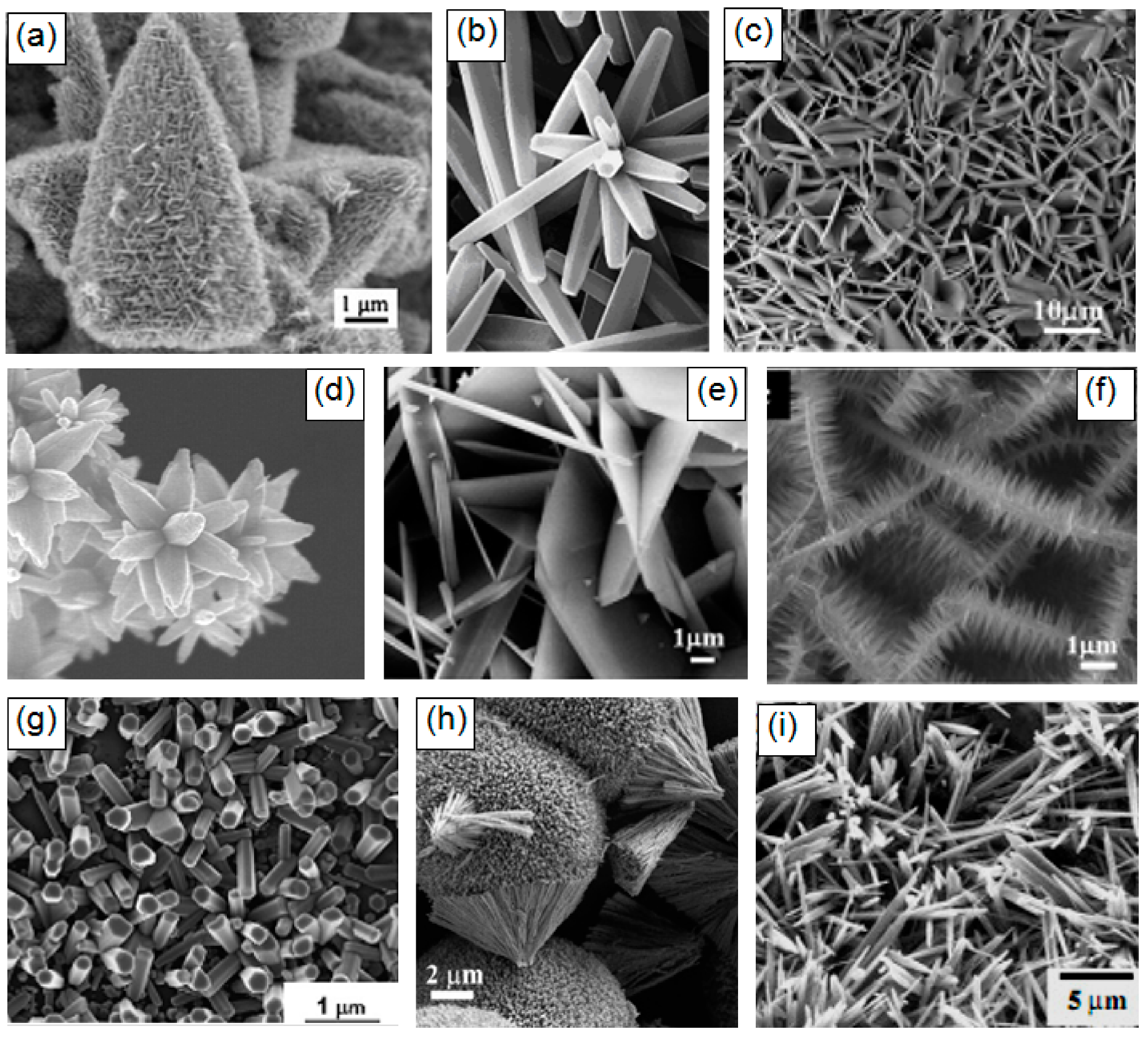
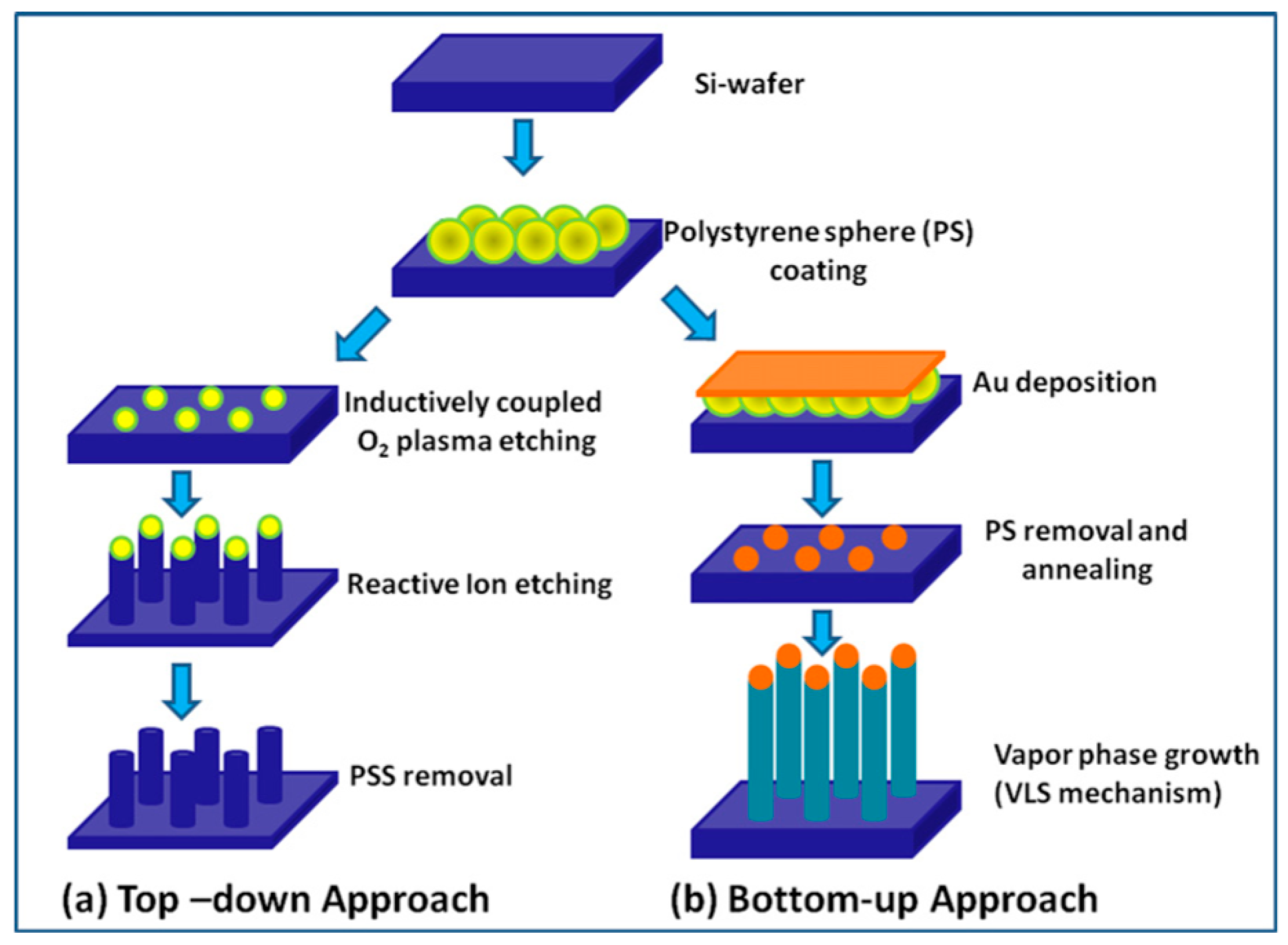
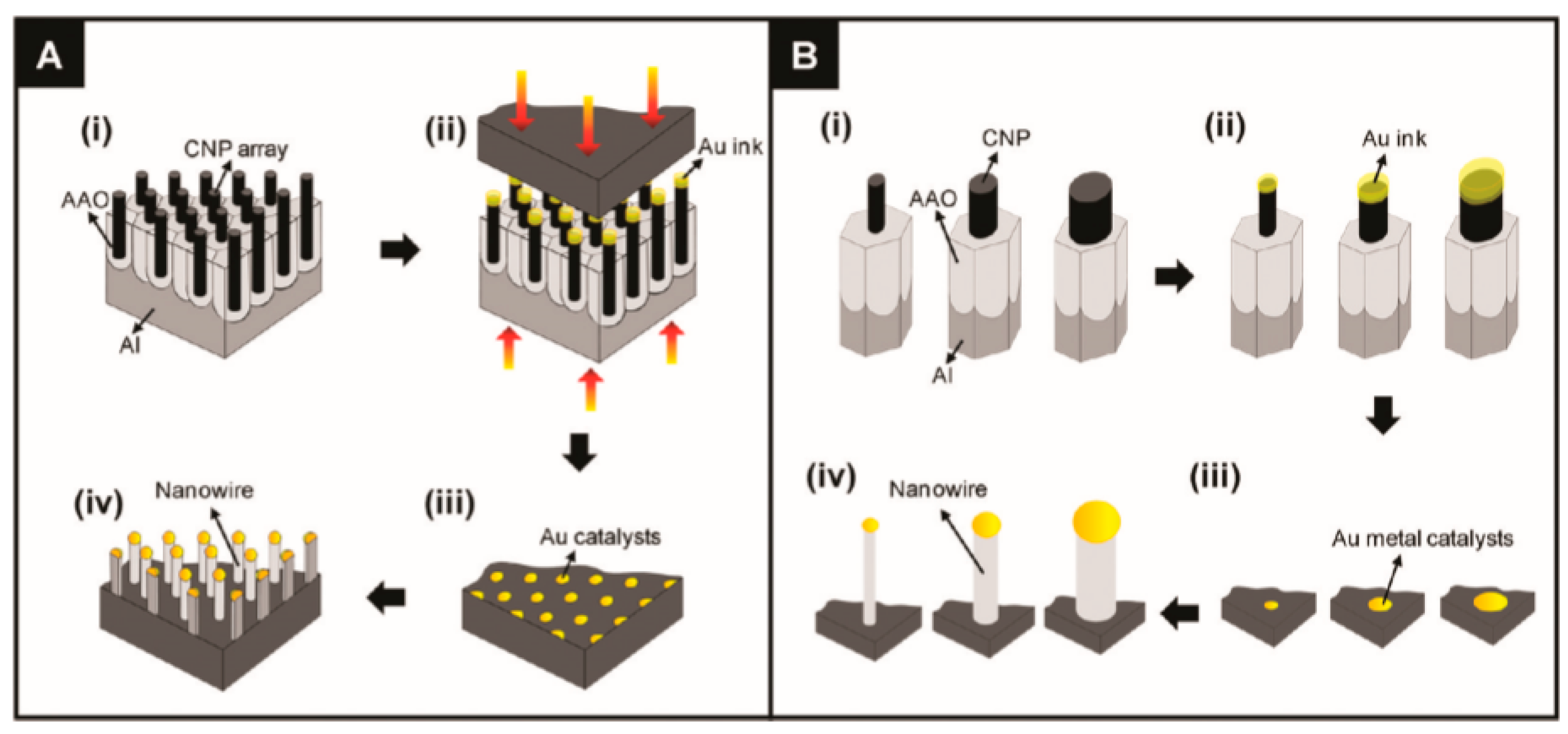
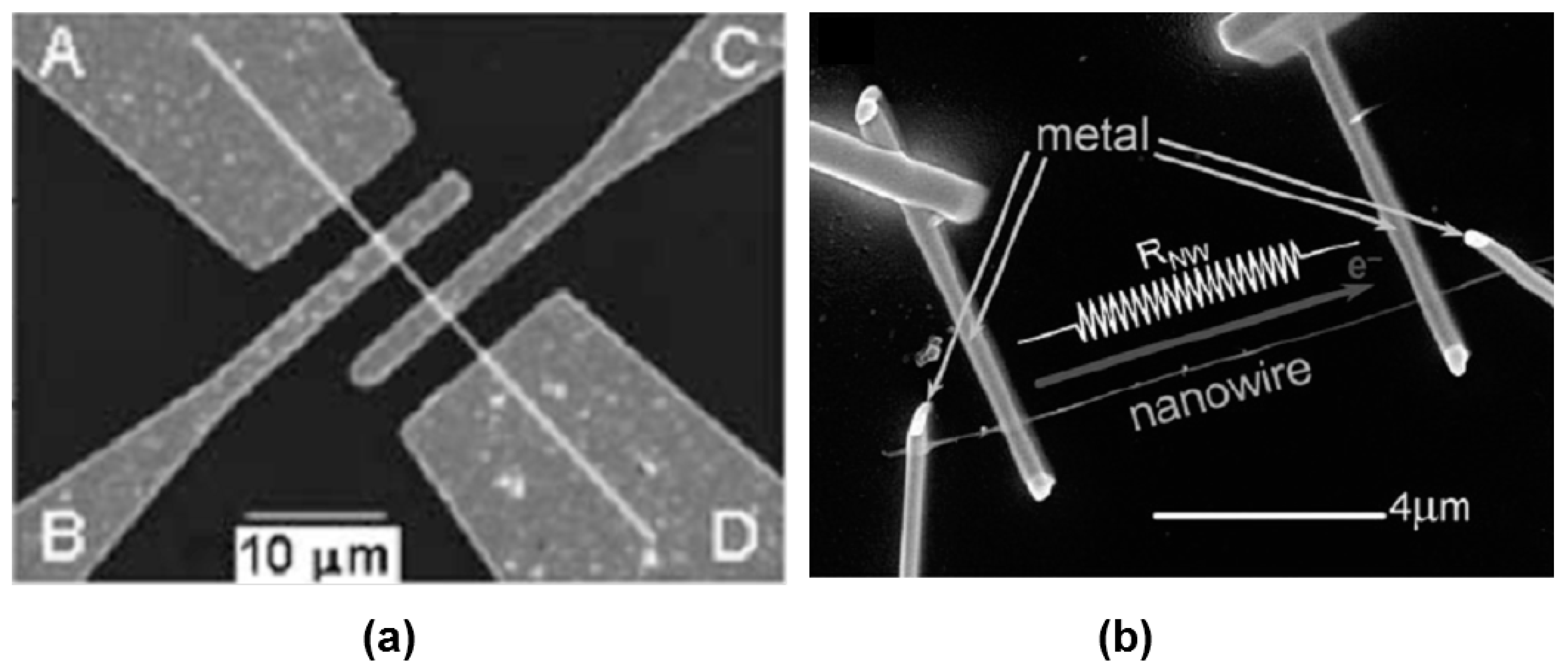
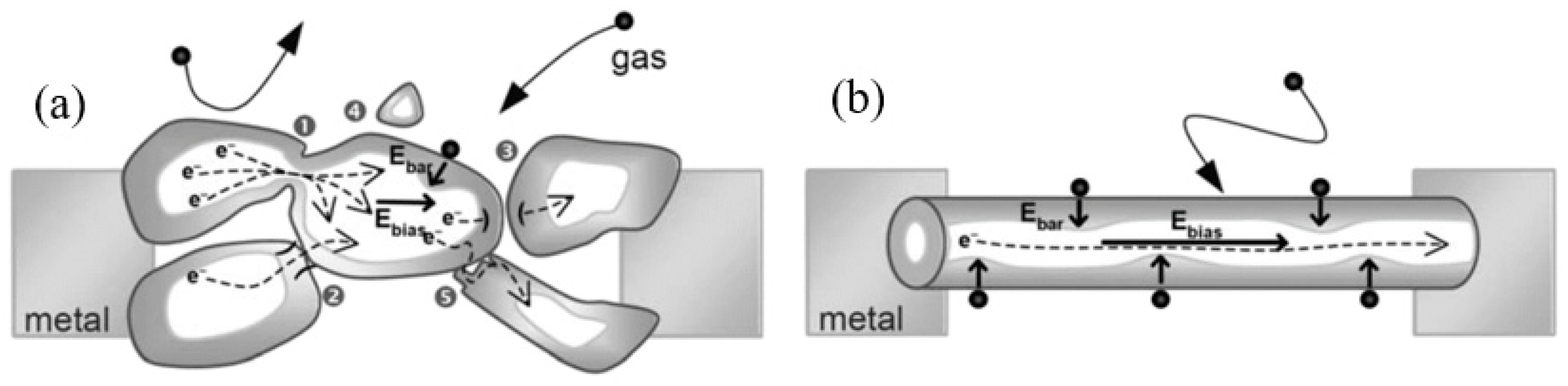
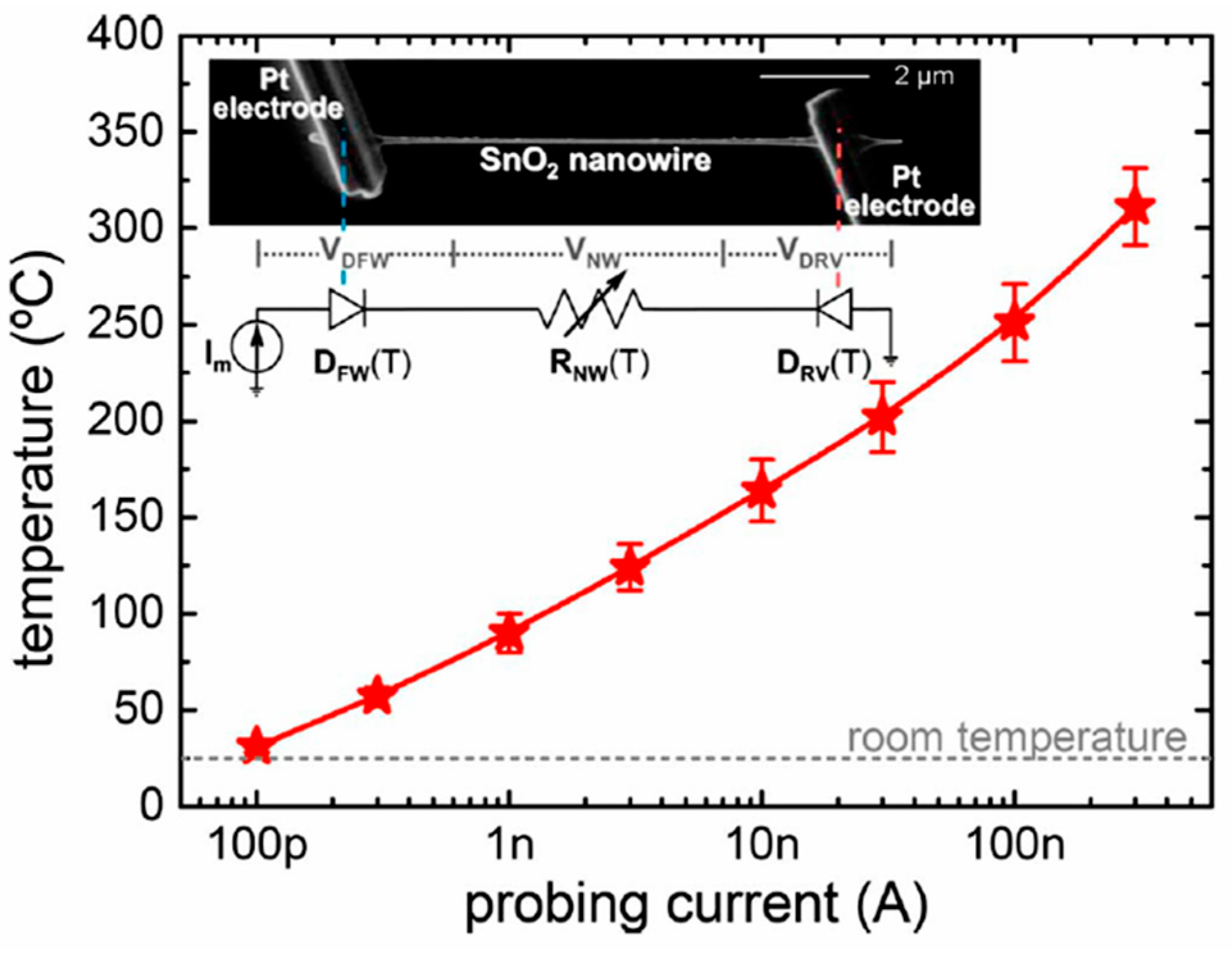
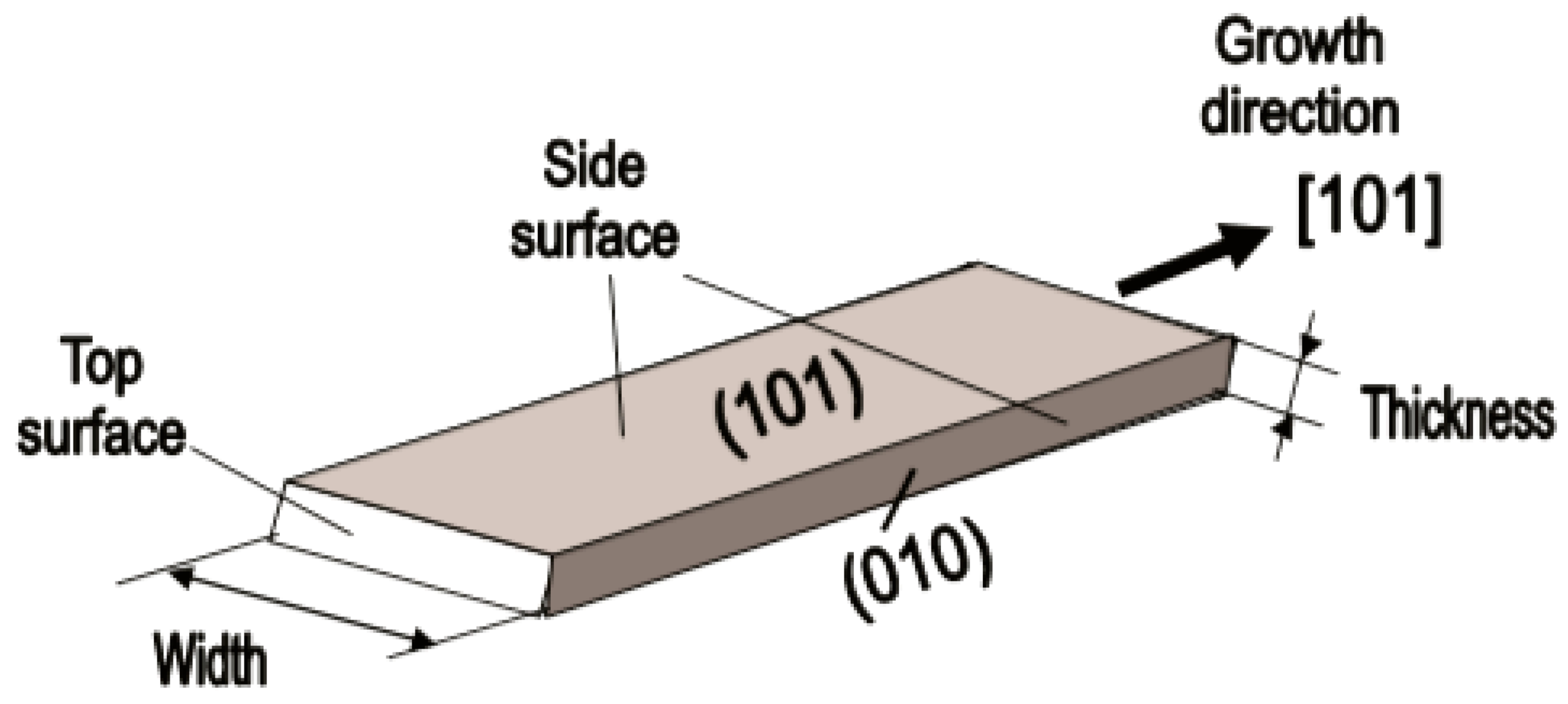
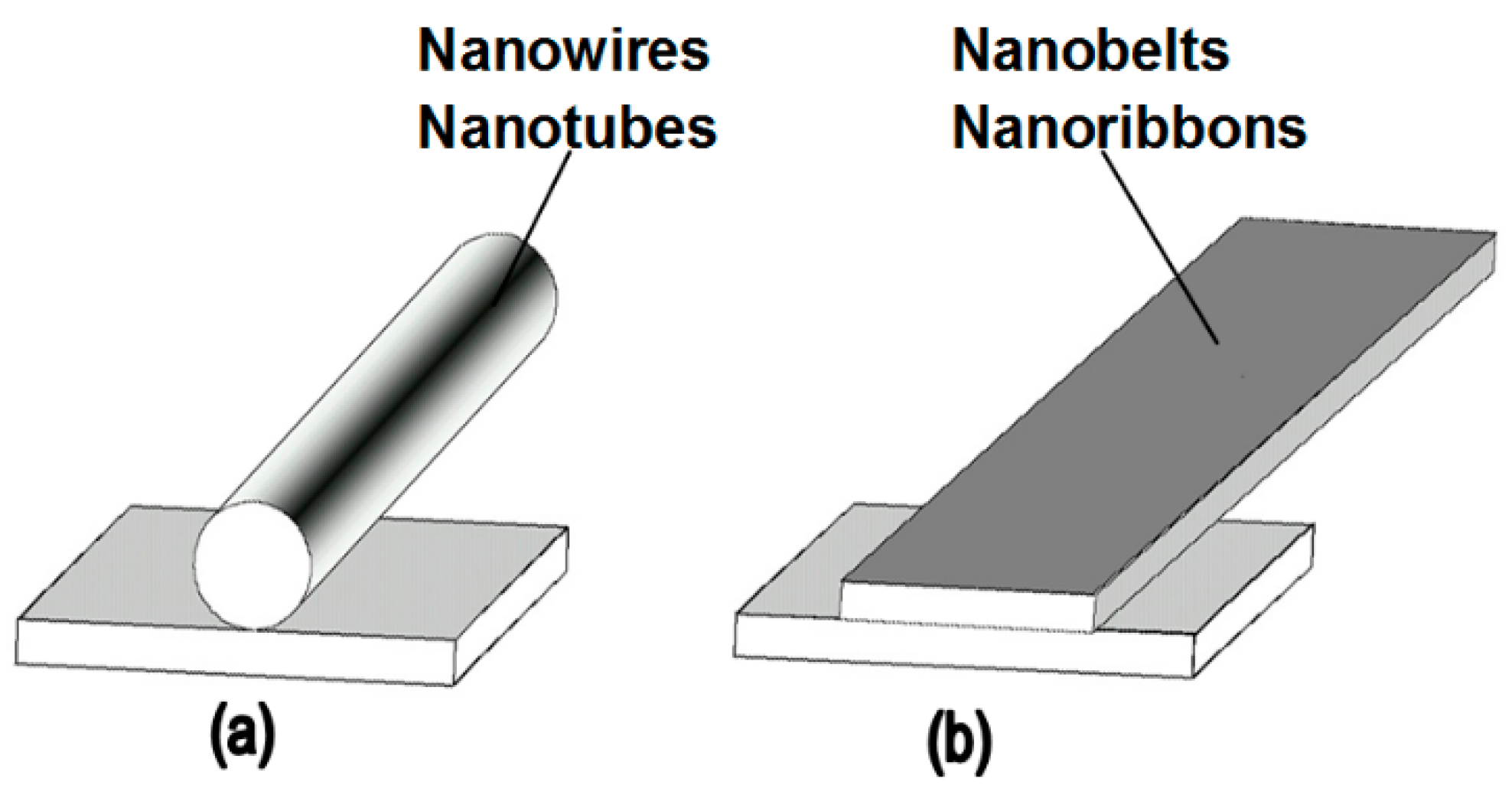
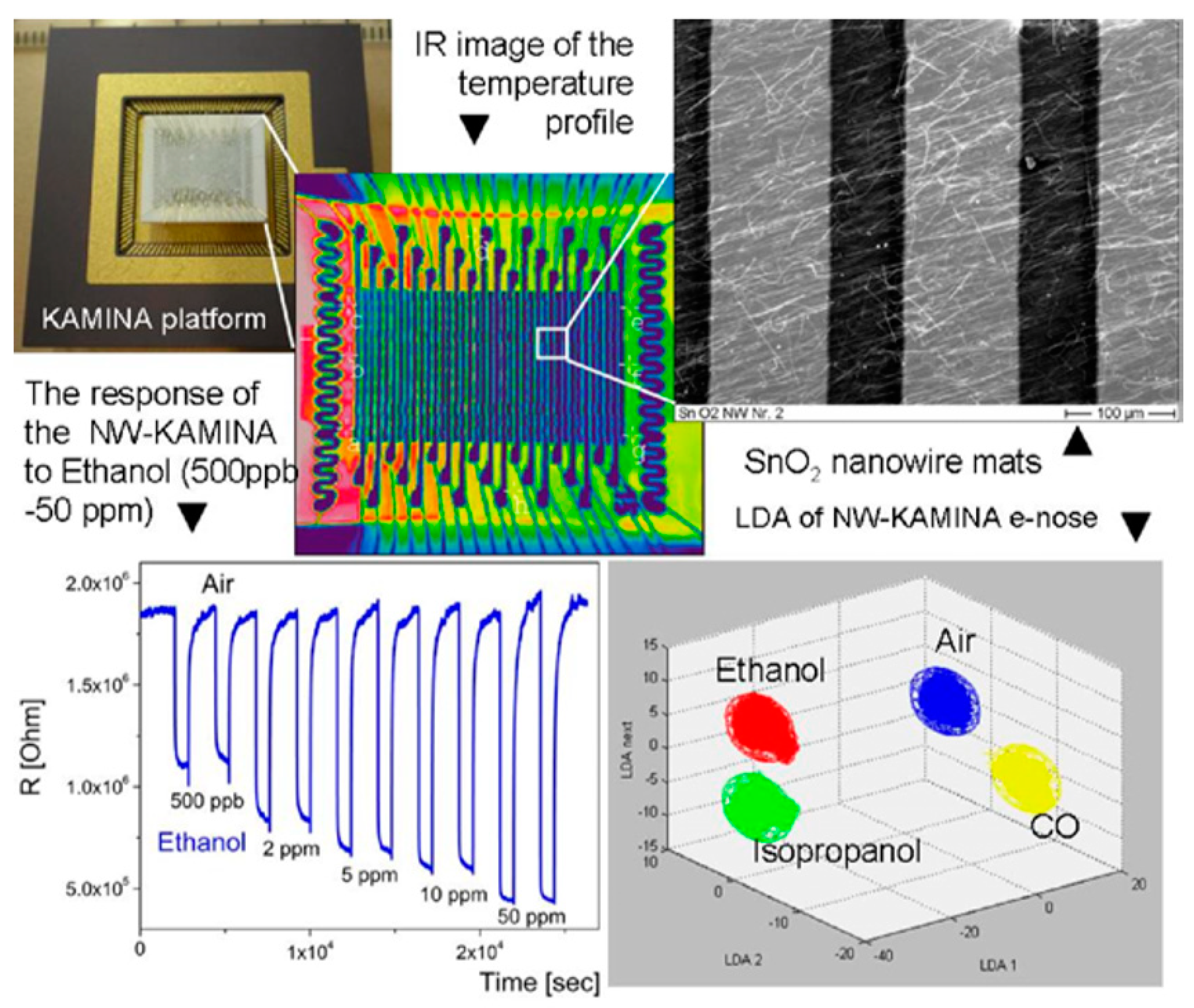
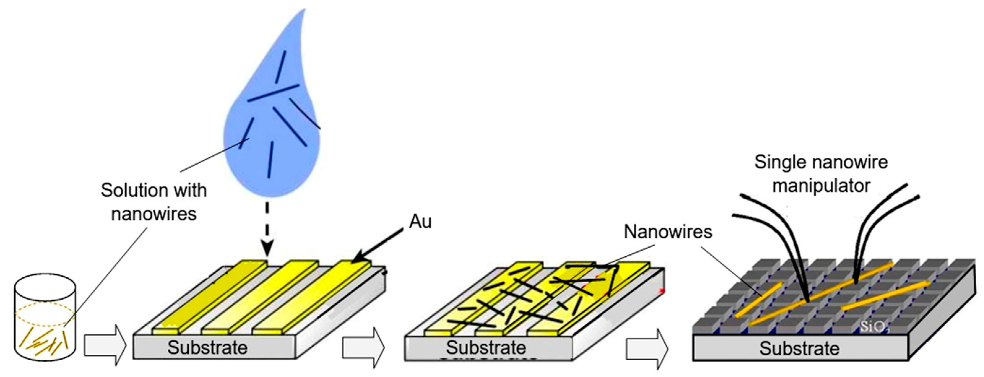
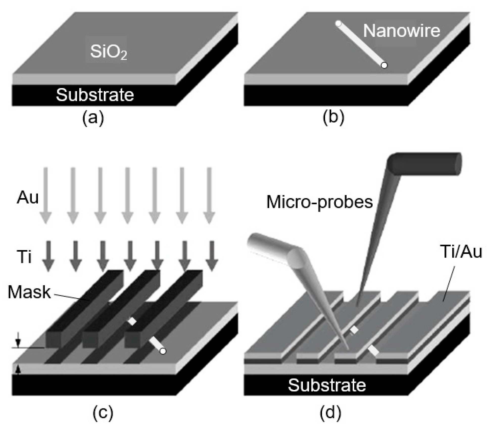
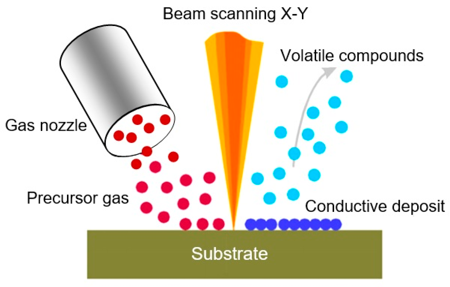
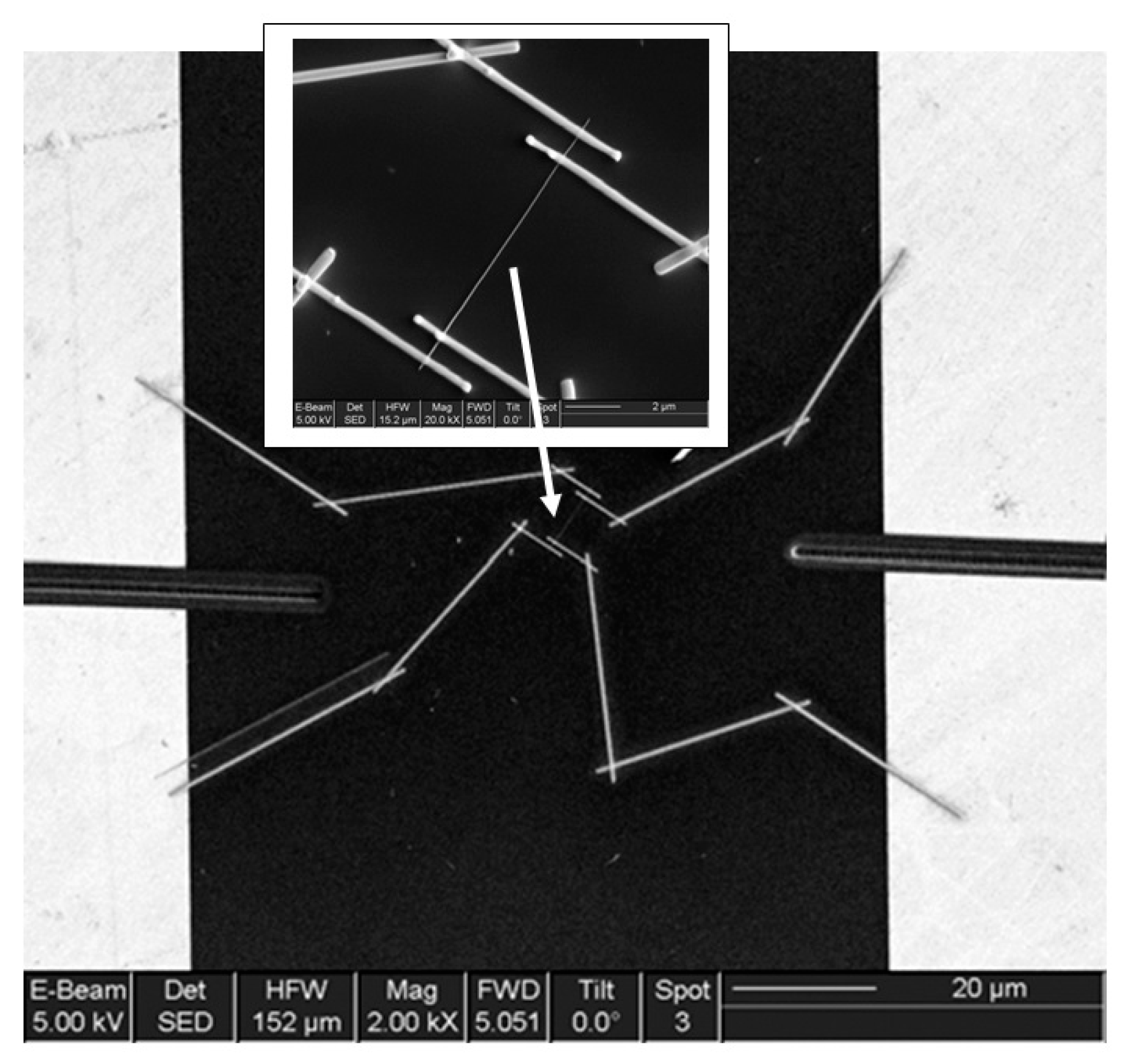
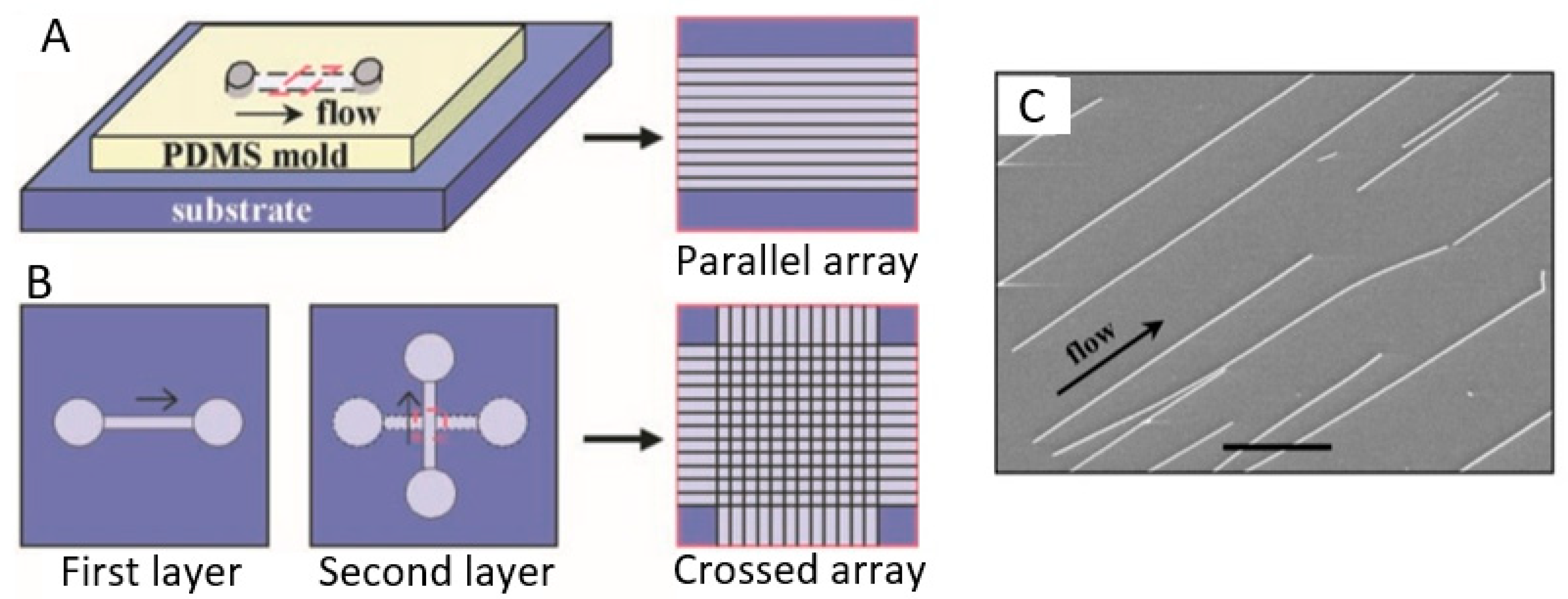
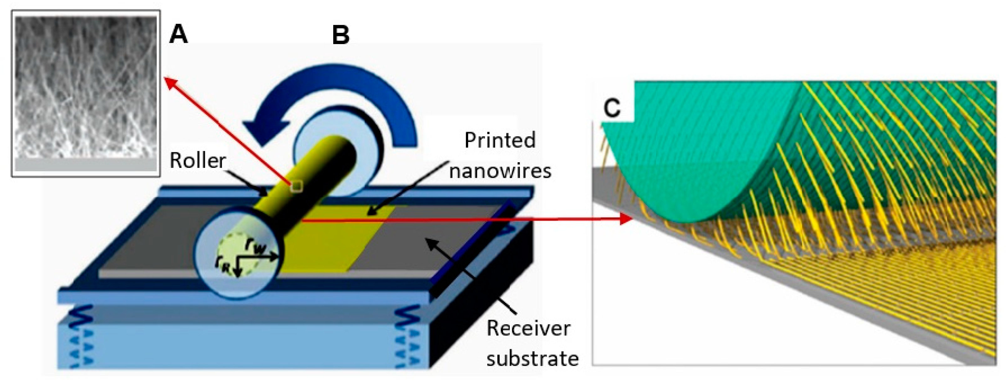
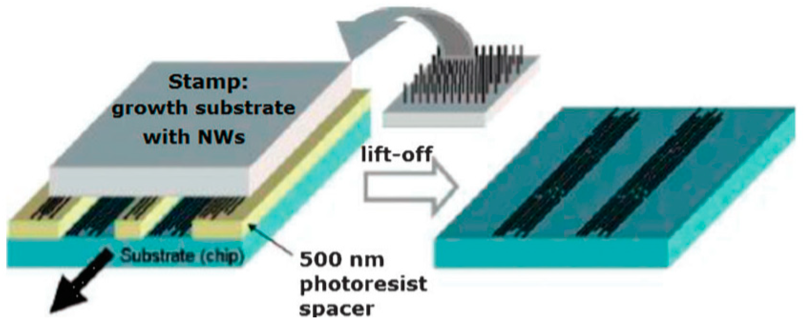
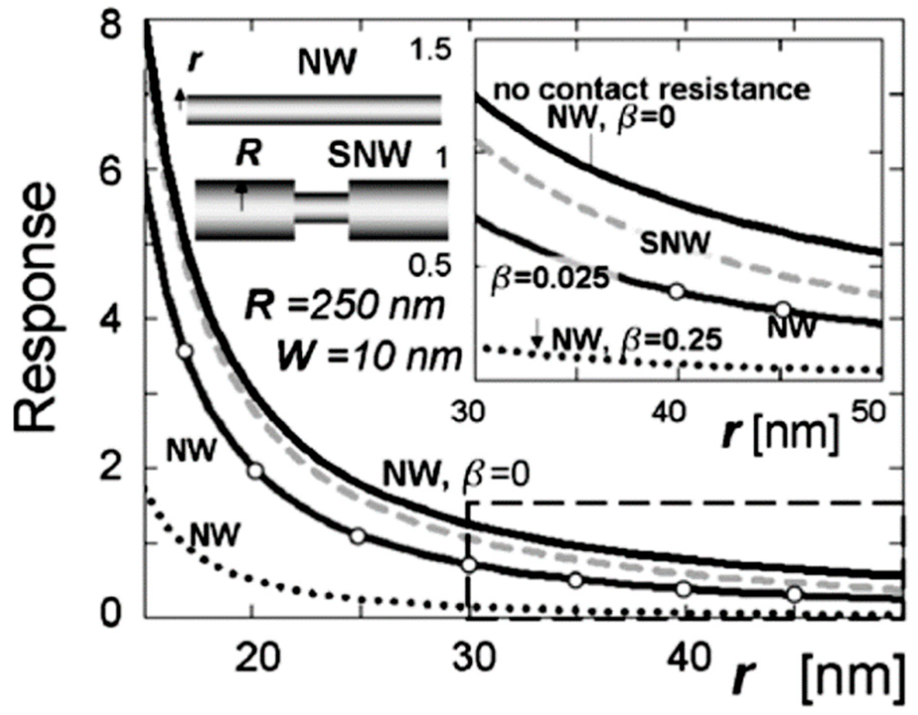
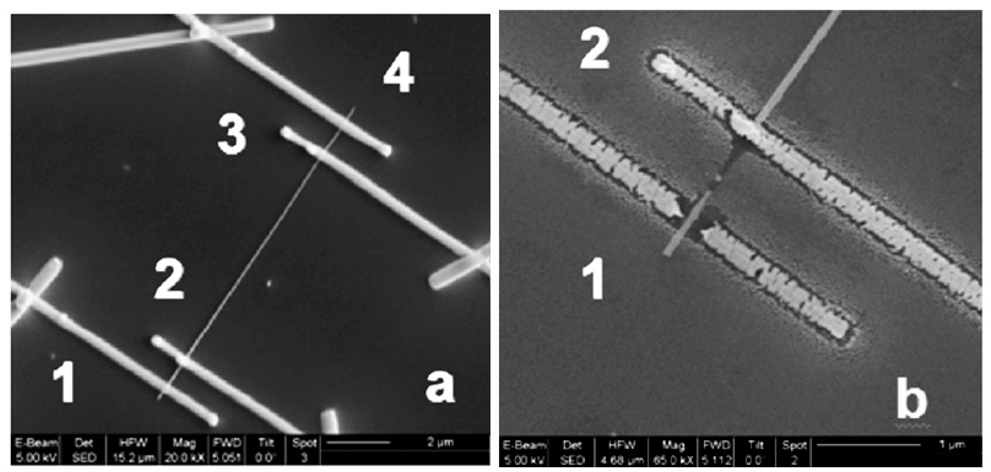
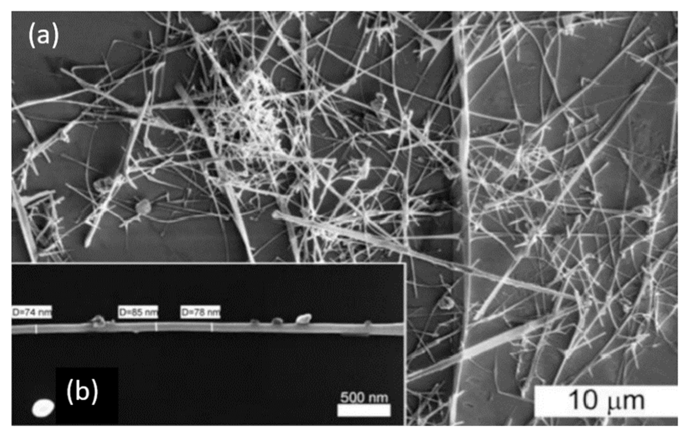
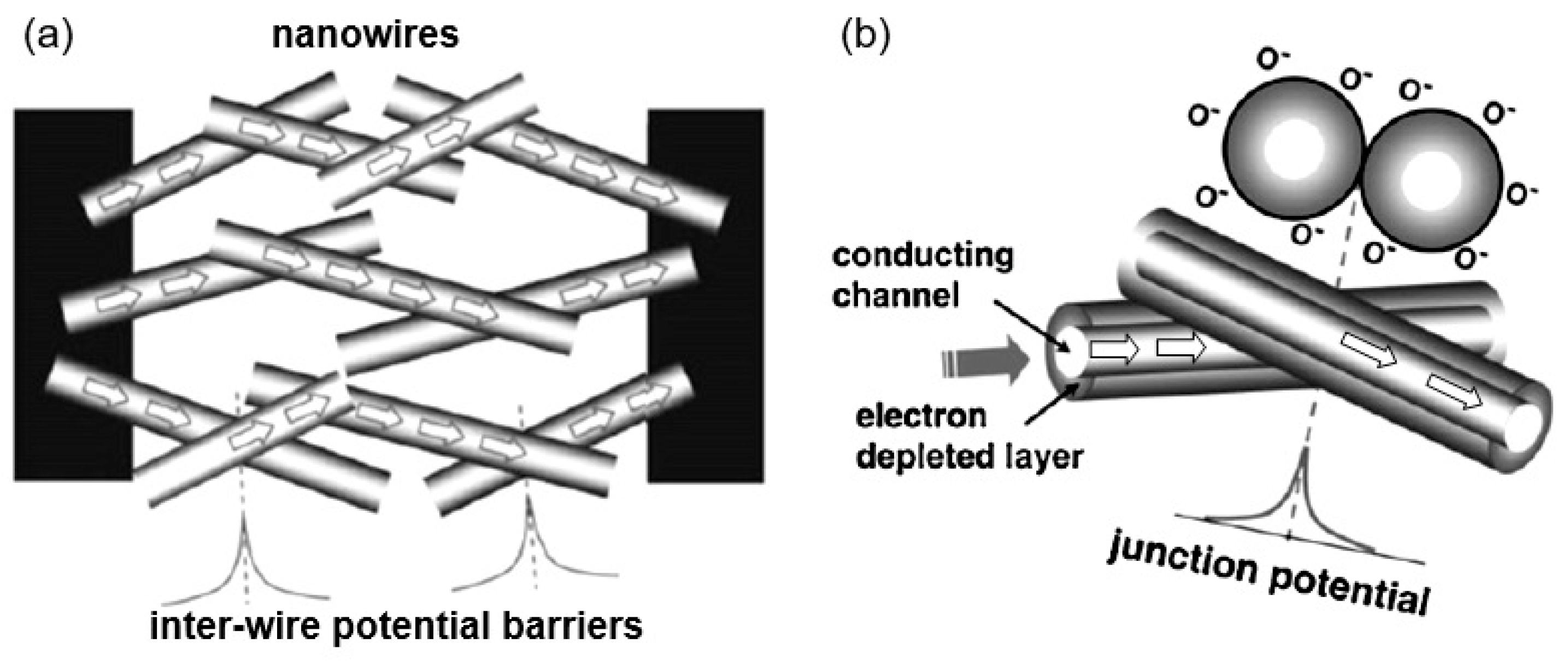
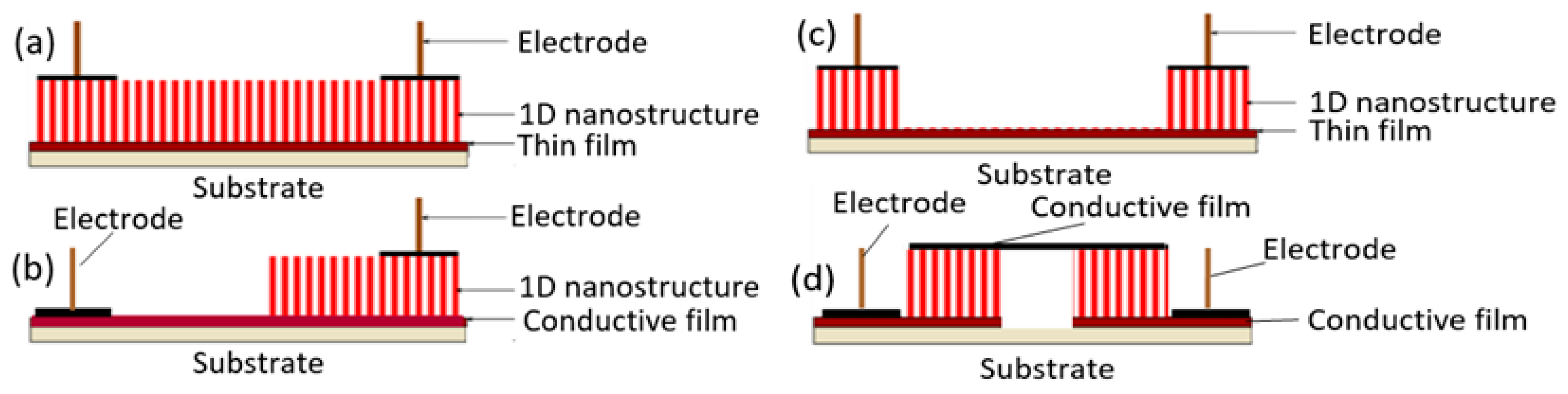
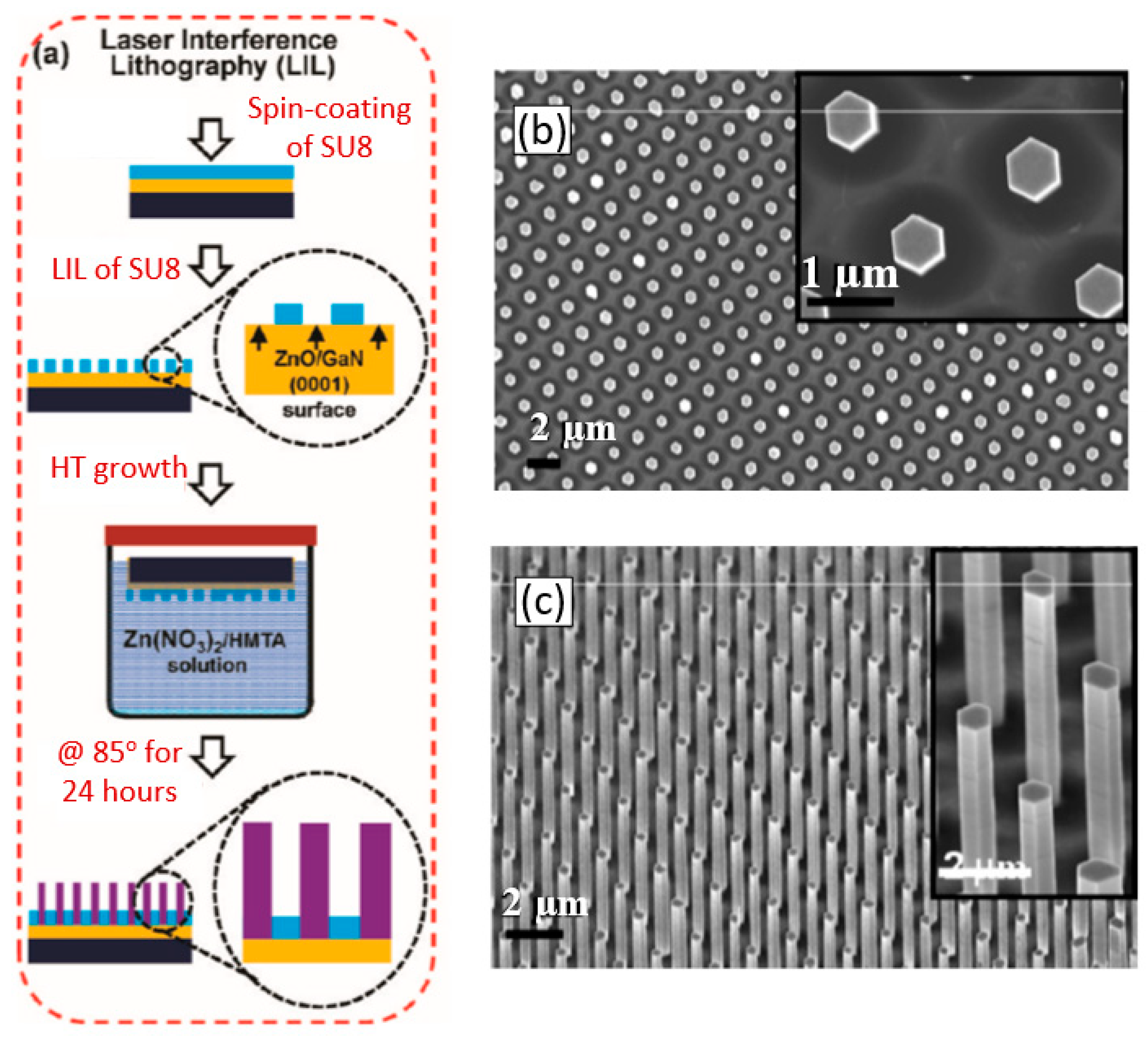
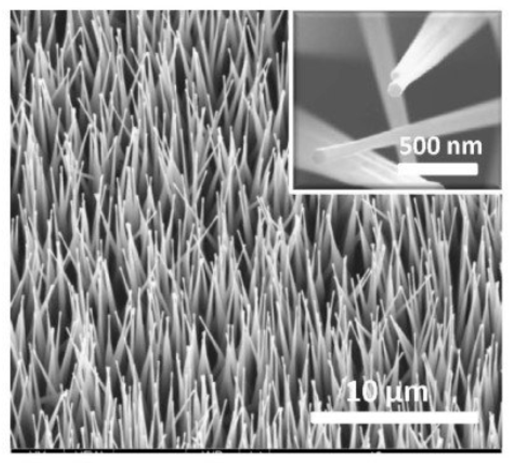
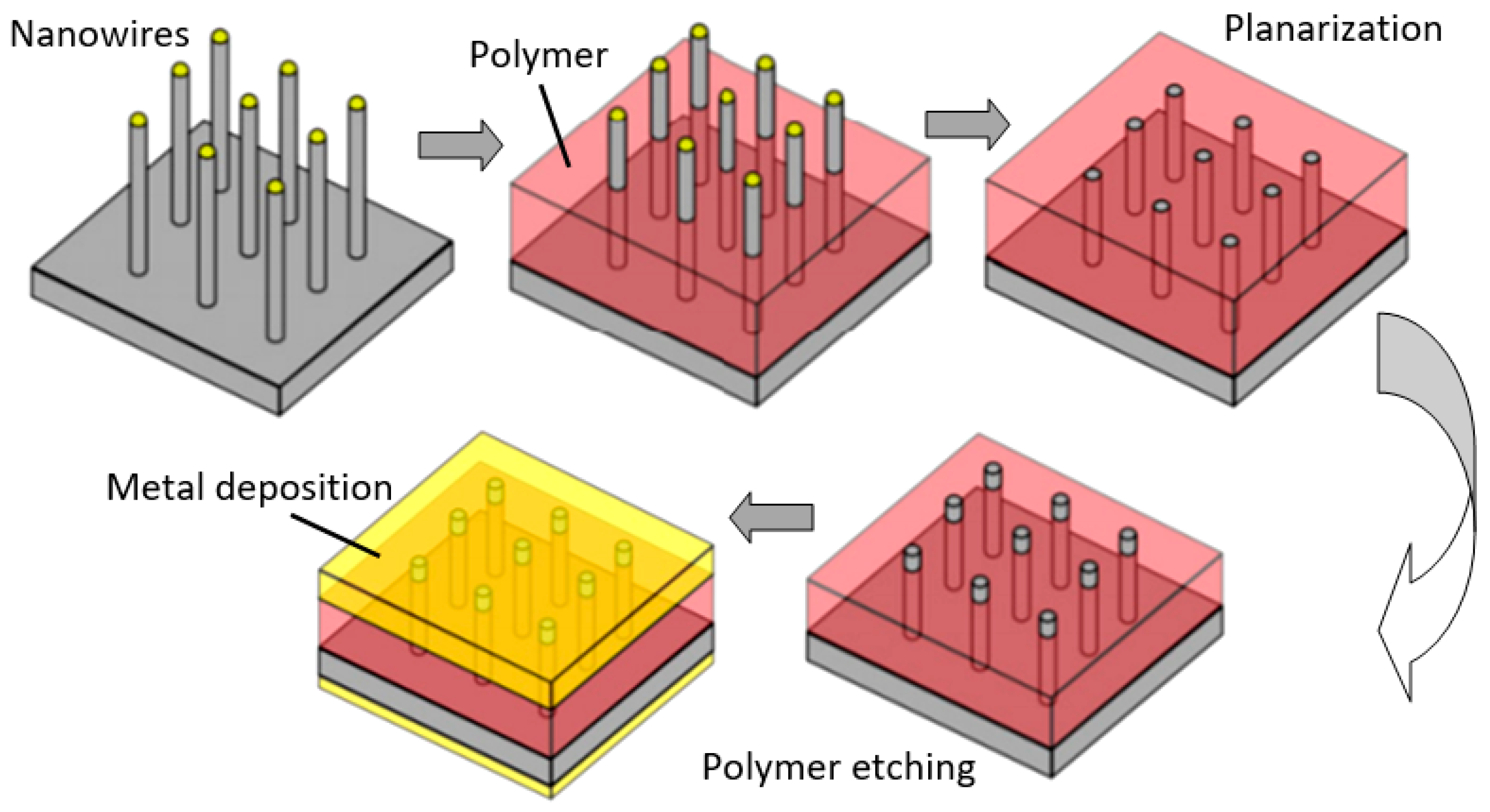
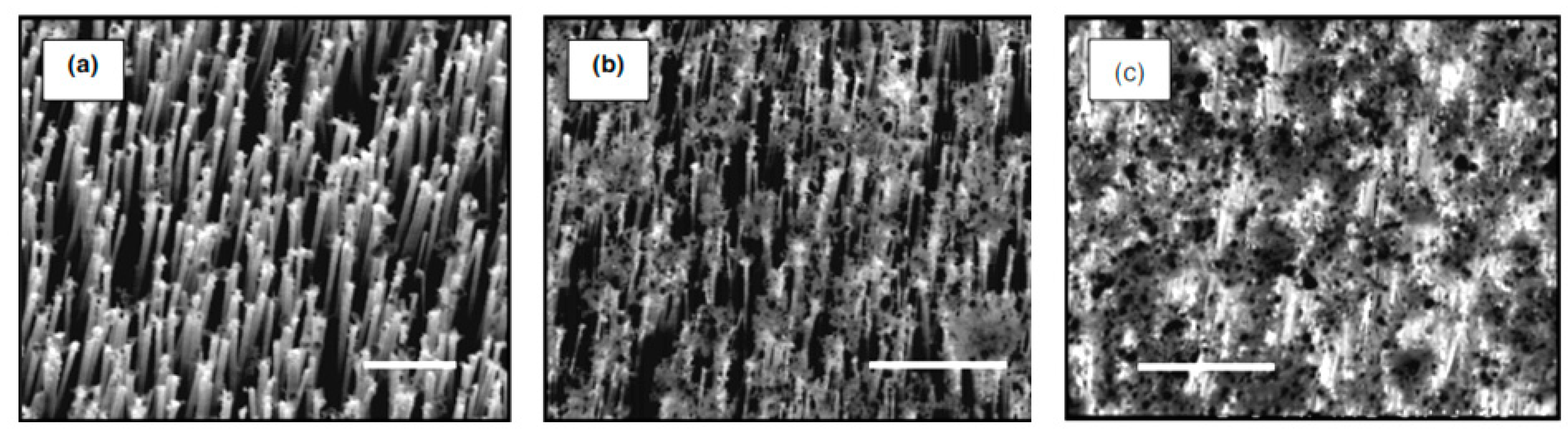
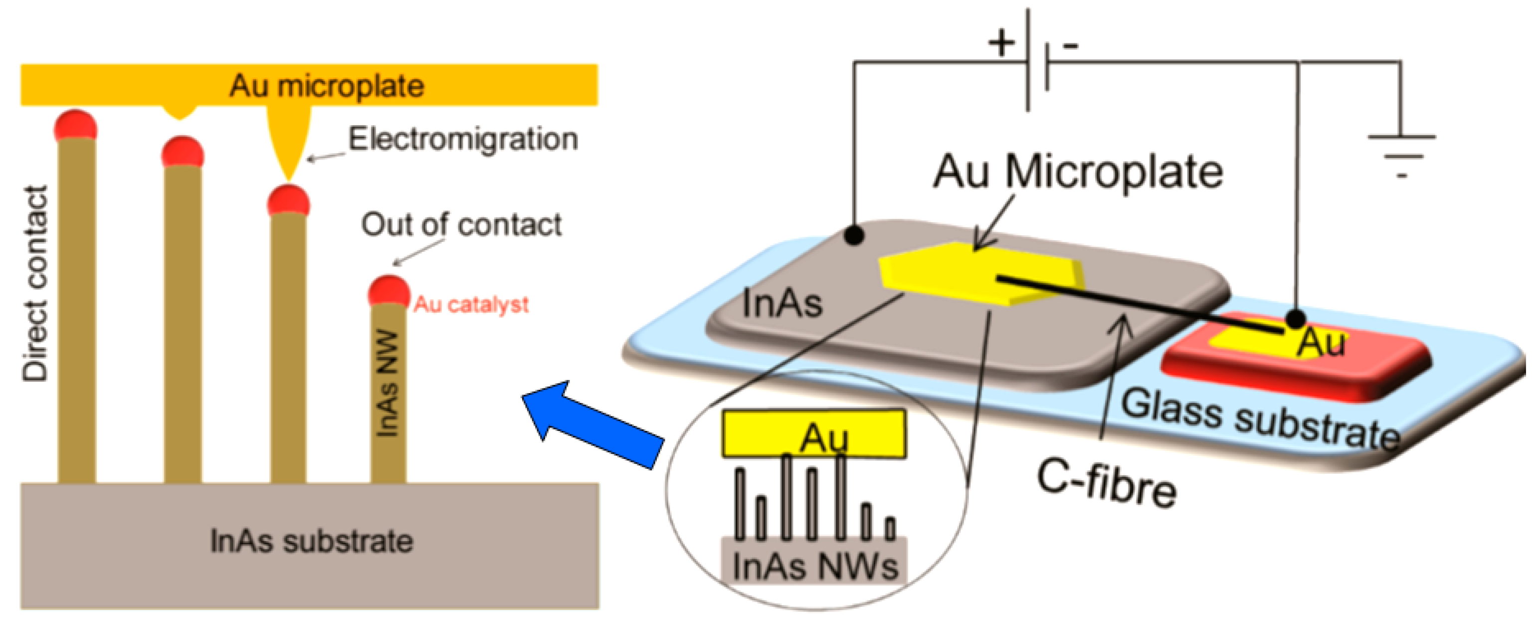
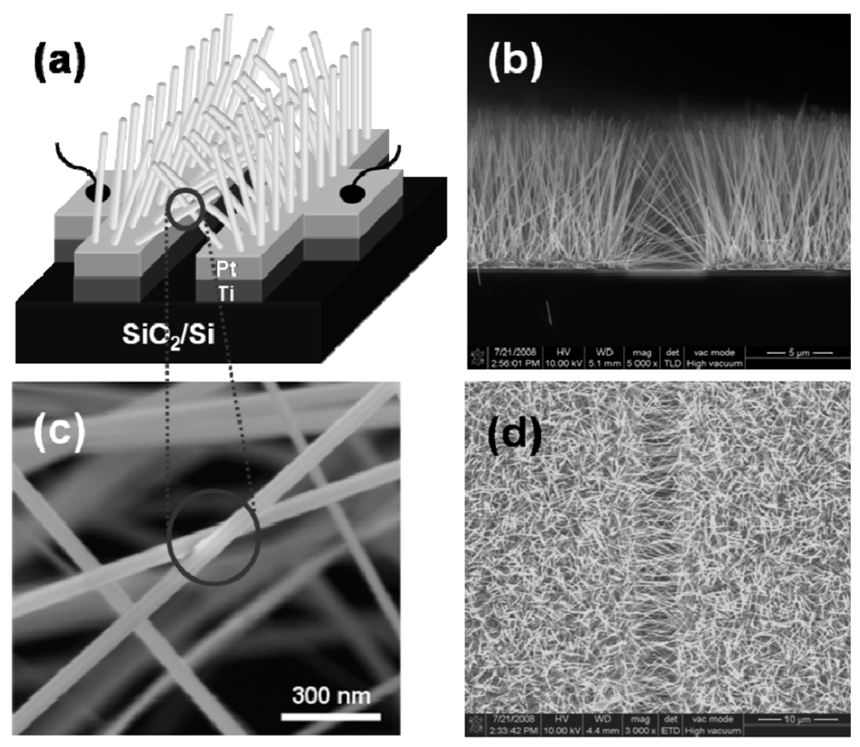
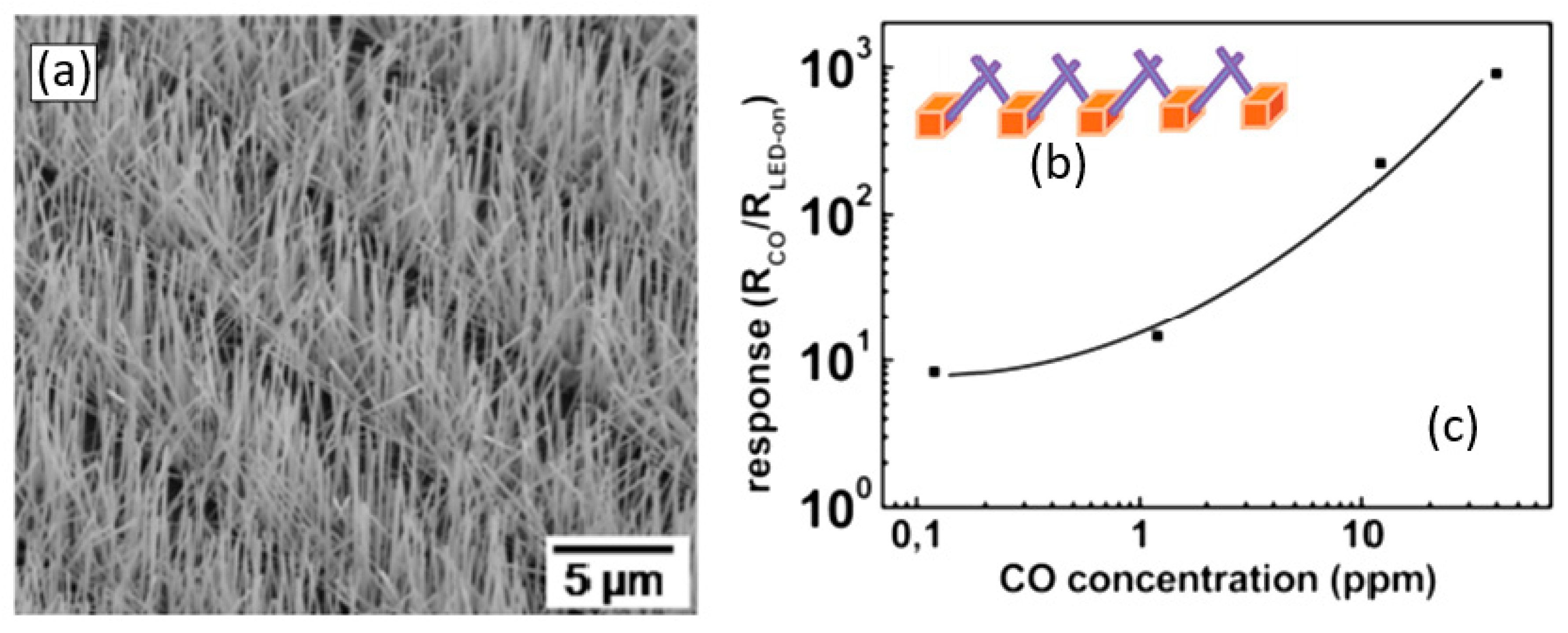
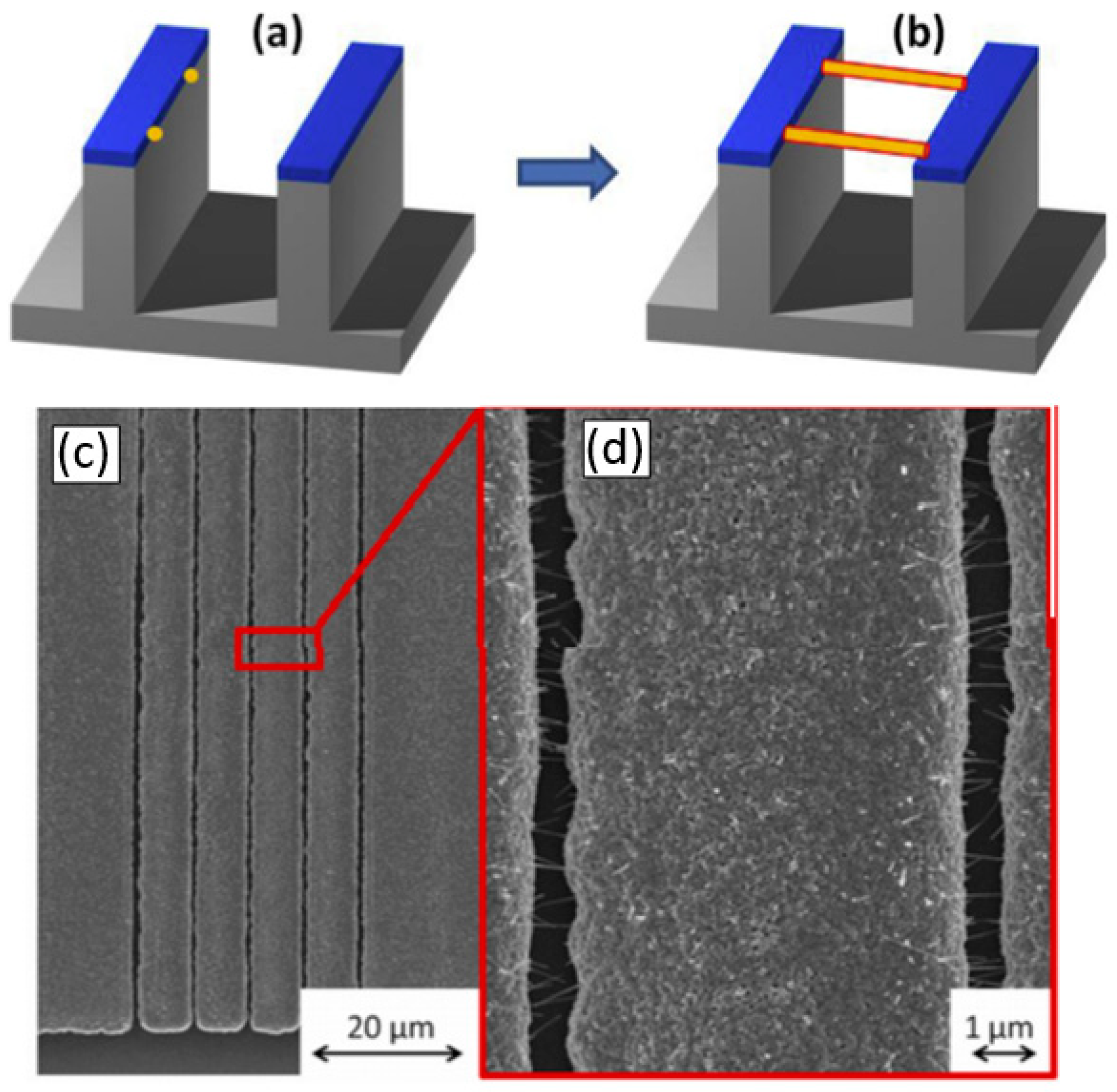
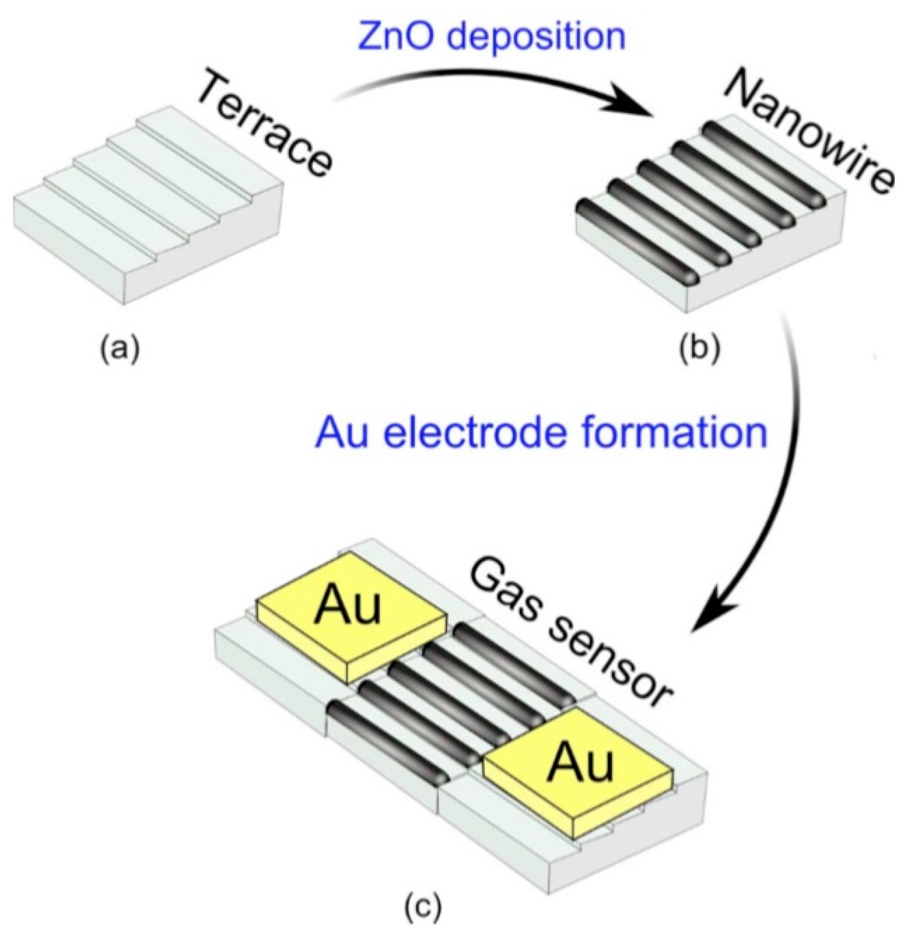
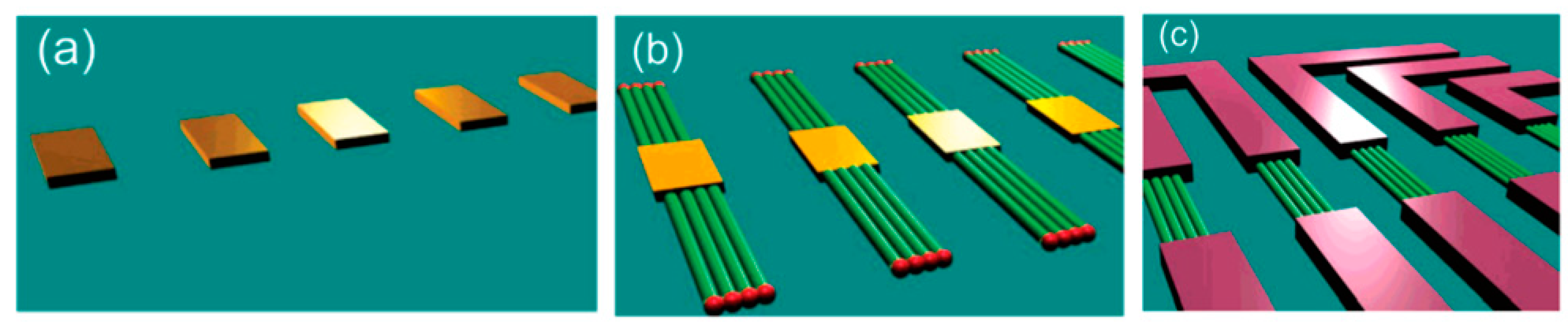
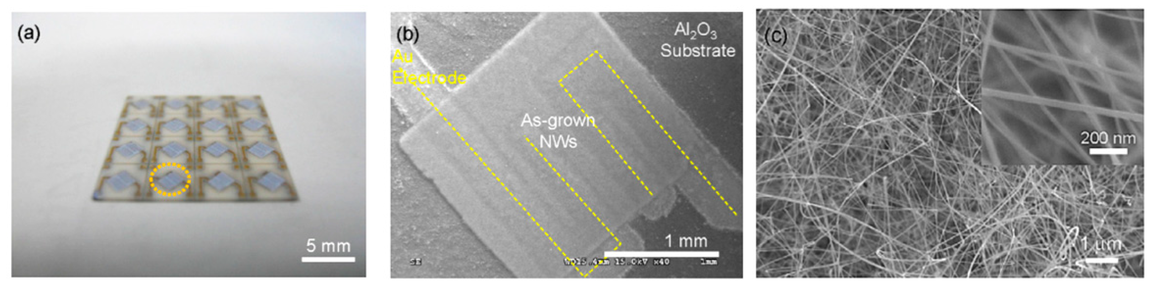
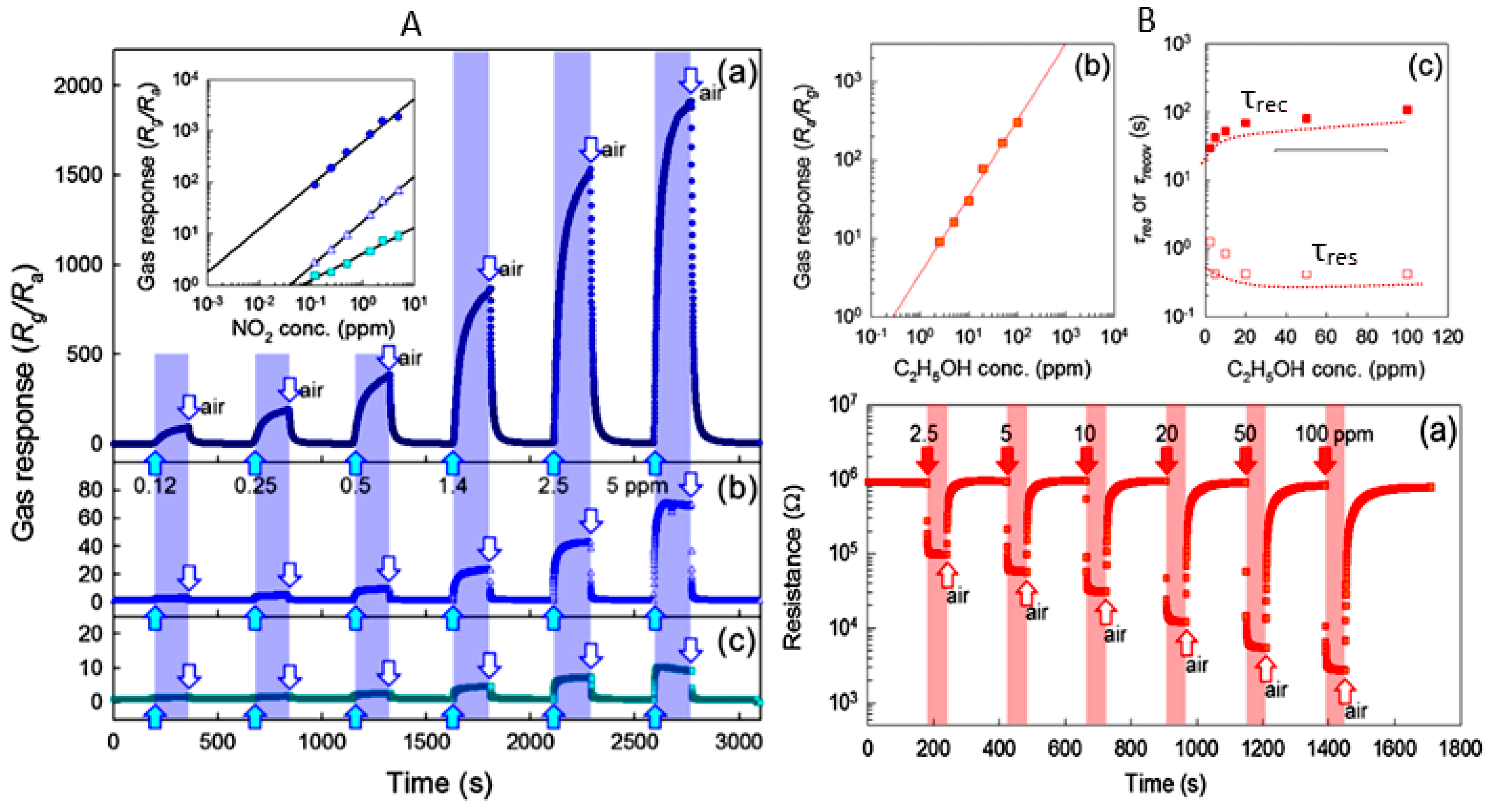
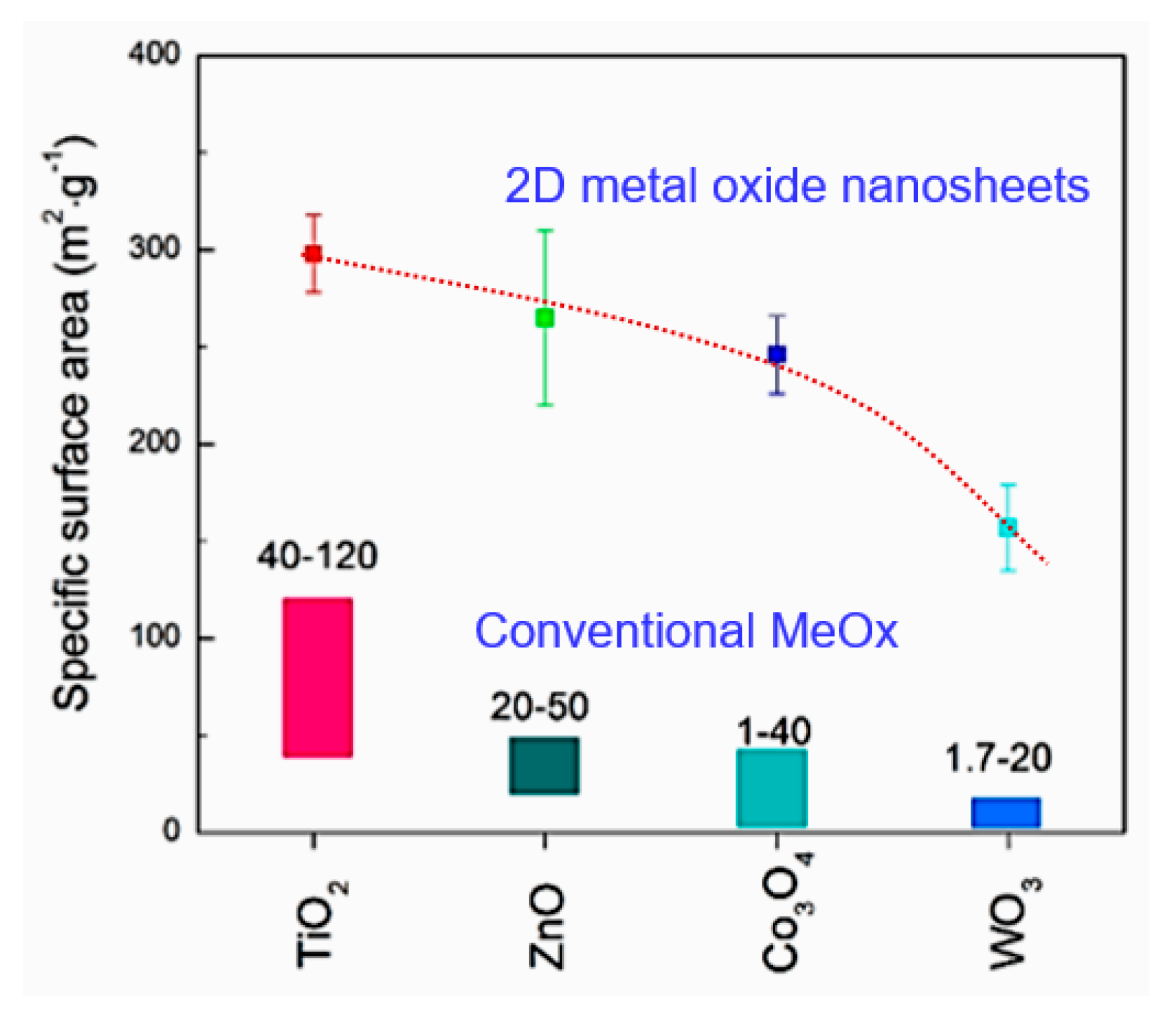
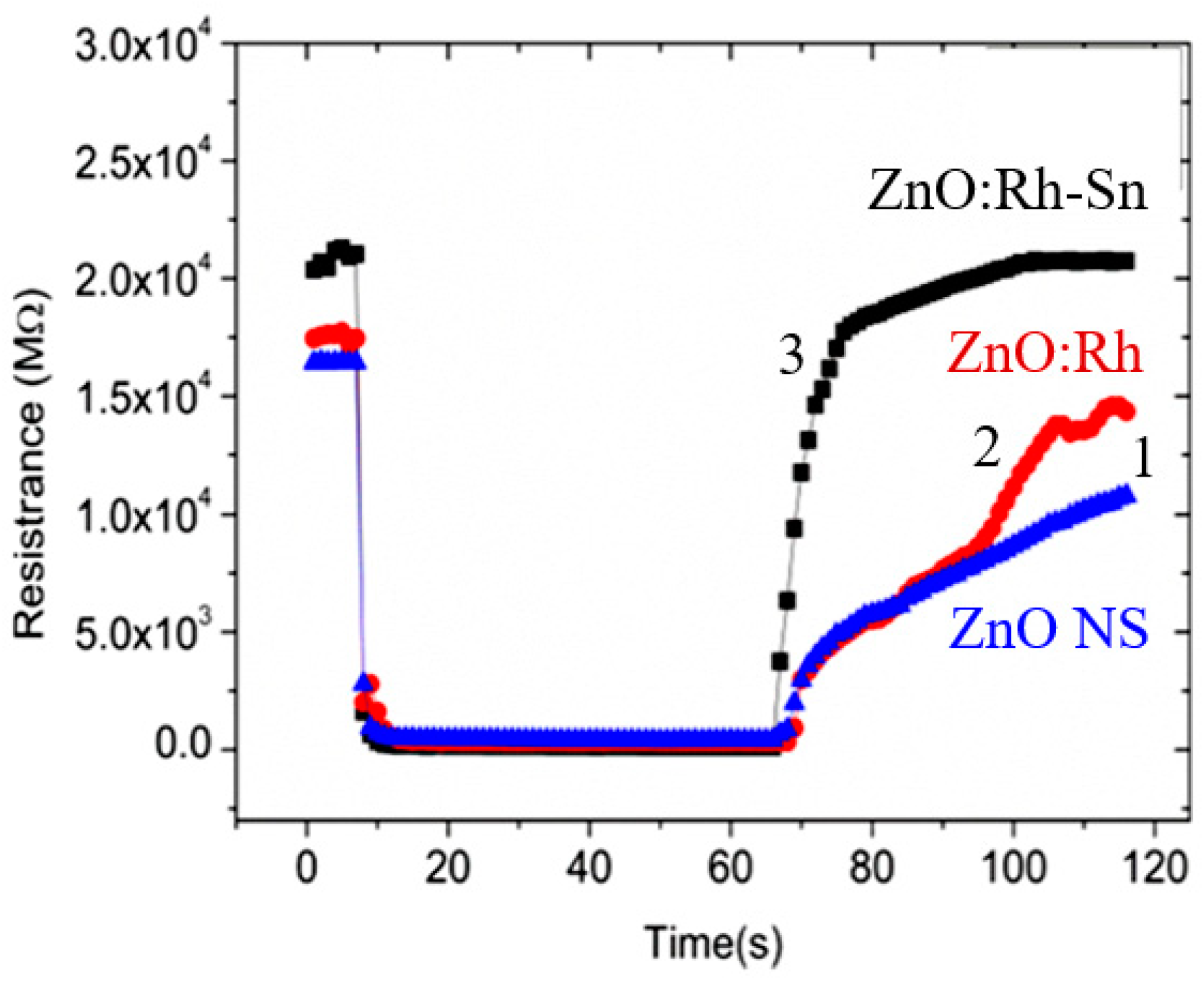
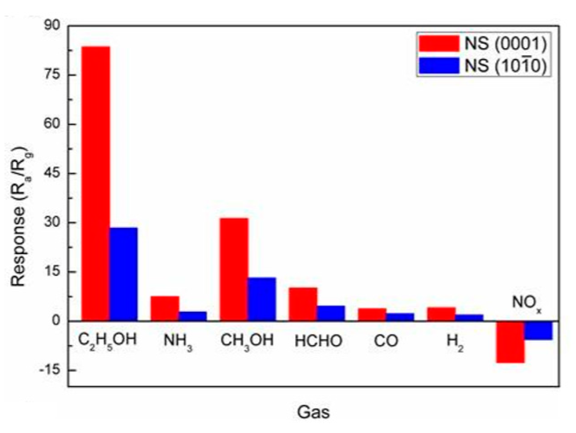
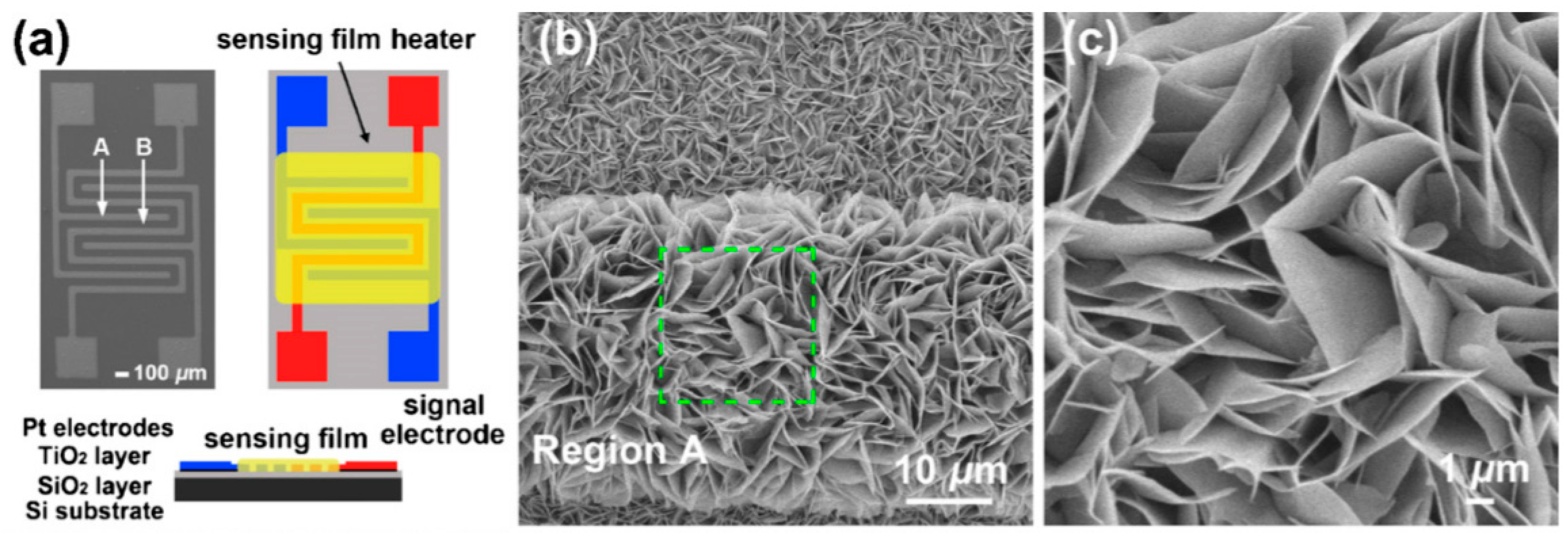
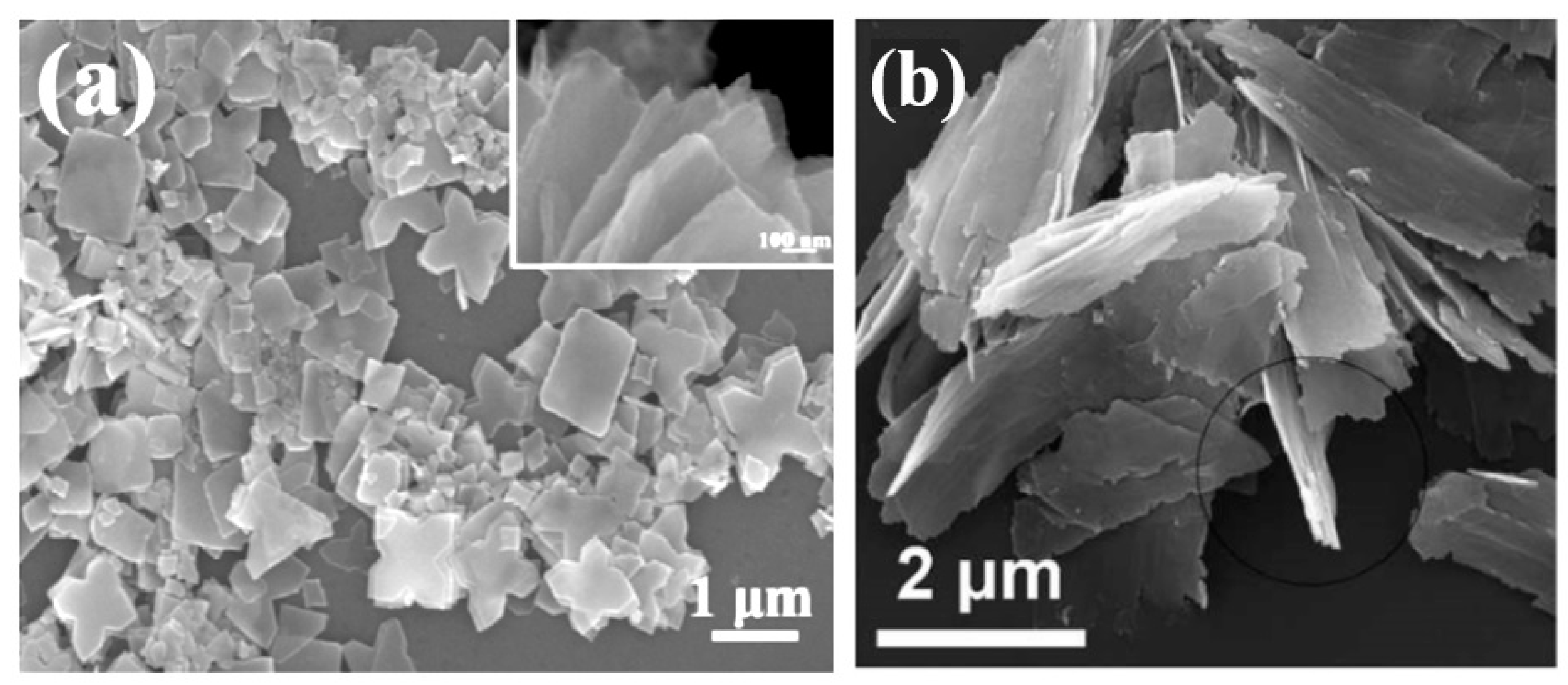
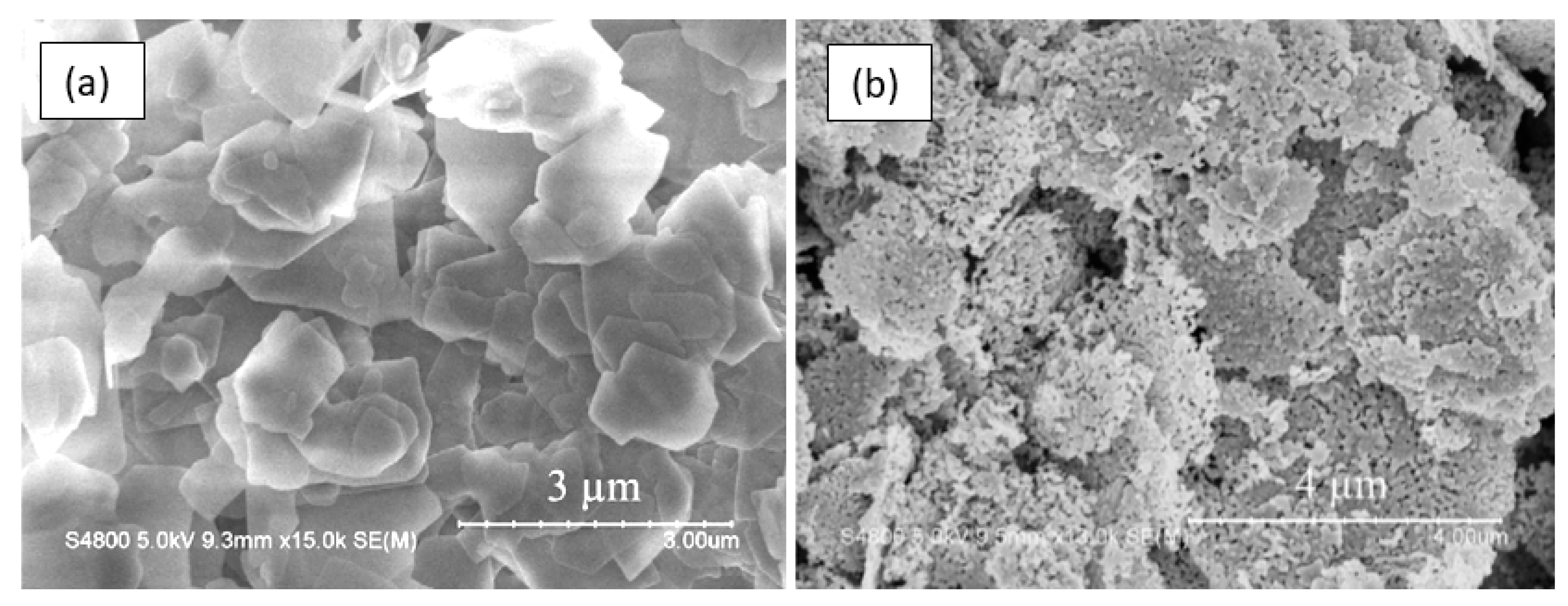
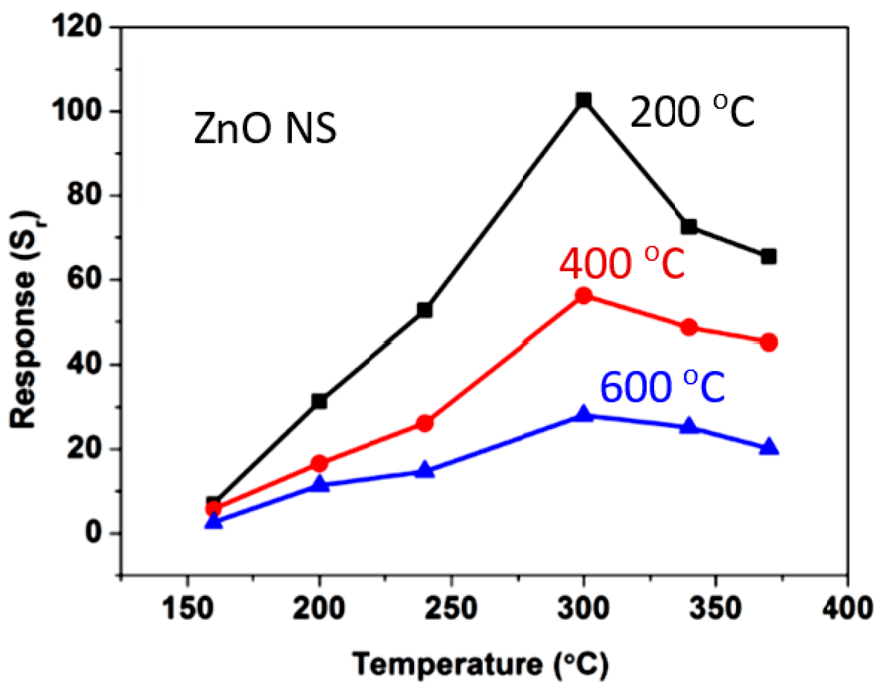
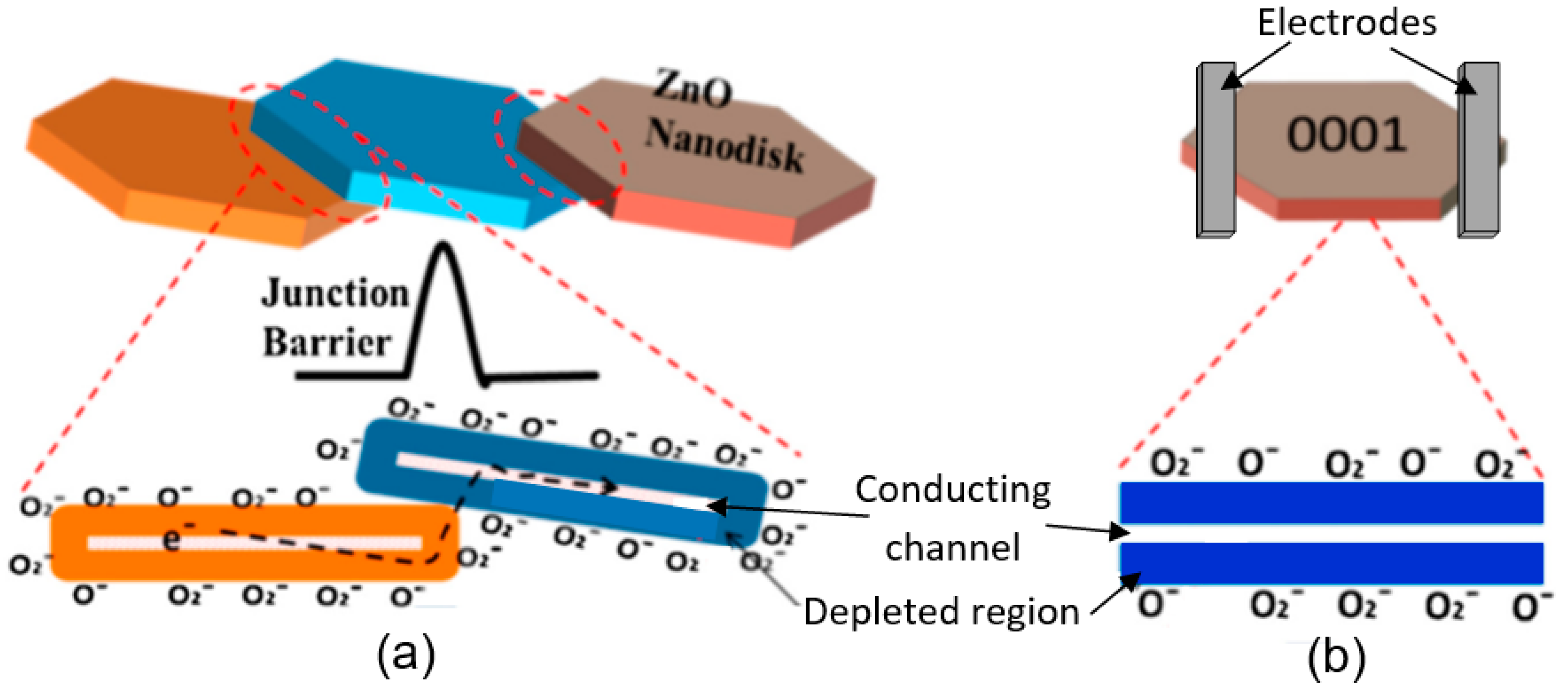
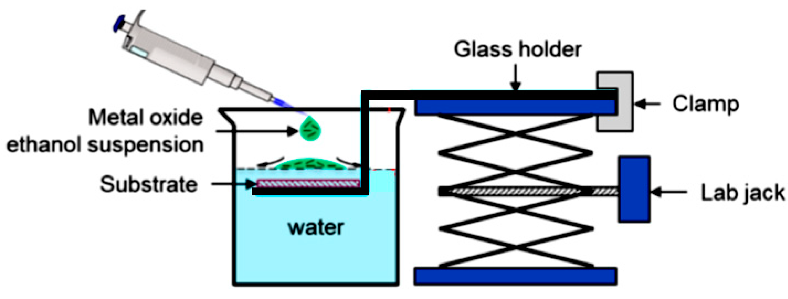
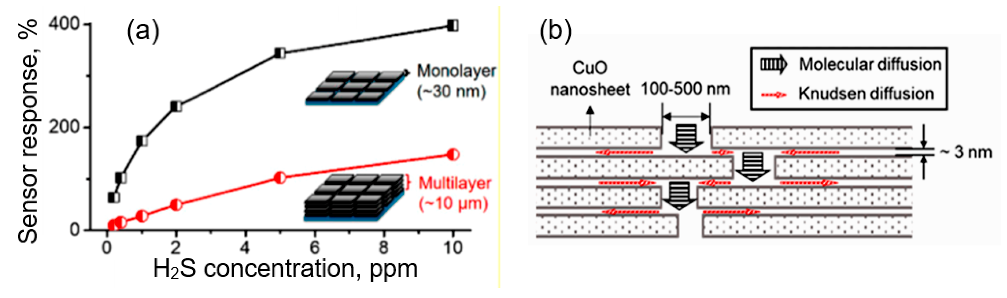
| Gas | Material | D, nm | Sensor Type | Toper, °C | DL, ppm | Response | τres, s | Ref. |
|---|---|---|---|---|---|---|---|---|
| NO2 | SnO2 (NWs) | 35–45 | R | 25 (UV) | <0.1 | 2 @ 5 ppm | ~60 | [152] |
| 175 | ~2 @ 10 ppm | |||||||
| SnO2 (NWs) | 30–100 | R | 240 | <0.01 | 500 @ 1 ppm | ~60 | [153] | |
| In2O3 (NWs) | ~10 | FET | 25 | 0.5 | 106 @ 100 ppm | 5–600 | [154] | |
| In2O3 (NWs) | ~10 | FET | 25 | 0.005 | ~1.6 @ 200 ppb | 50–1000 | [155] | |
| H2 | SnO2 (NWs) | 50–200 | R | 300 | <5.0 | 25 @ 50 ppm | <120 | [156] |
| CO | SnO2 (NBs) | 60 | R | 400 | ~5.0 | 70 @ 250 ppm | 30 | [157] |
| SnO2 (SNW) | 25–70 | R | 300 | <1.0 | 2.1 @ 200 ppm | N/A | [158,159] | |
| ZnO:Pd (NWs) | 60–70 | R | 20 | <0.1 | 1.2 @ 0.1 ppm | >240 | [160] | |
| H2S | SnO2:Cu (NWs) | 10–100 | R | 150 | <1.0 | ~107 @ 80 ppm | N/A | [161] |
| In2O3 (NWs) | 30–100 | FET | 120 | <1.0 | ~12 @ 20 ppm | >300 | [162] | |
| CuO (NWs) | 20–40 | R | 325 | ~0.01 | 4 @ 500 ppb | ~600 | [163] | |
| ZnO (NWs) | ~20 | R | 300 | 0.005 | ~2 @ 200 ppb | ~270 | [164] | |
| C2H5OH | ZnO:Mg (NWs) | ~120 | R | 350 | ~0.01 | 343 @ 5 ppm | ~20 s | [165] |
| SnO2 (NWs) | 30–100 | R | 300 | <1.0 | 100 @ 20 ppm | <20 s | [153] | |
| NH3 | WO3 (NWs) | ~5 | R | 25 | ~0.1 | 1.1 @ 5 ppm | ~ 50 s | [166] |
| SnO2 (SNW) | ~100 | R | 300 | ~0.1 | ~2 @ 100 ppm | ~ 25 s | [167] |
| Nanostructures | Crystal Structure | Growth Direction | Top Surface | Side Surface |
|---|---|---|---|---|
| ZnO-belt | Wurtzite | (0001)or (010) | ±(20) | ±(010) or ±(0001) |
| Ga2O3-belt | Monoclinic | (001) or (010) | ±(100) | ±(010) or ±(10) |
| Ga2O3-sheet | Monoclinic | (101) (normal) | ±(100) | ±(010) ±(10) and ±(21) |
| t-SnO2-belt | Rutile | (101) | ±(10) | ±(010) and ±(10) |
| SnO2-belt | Rutile | (100) | ±(001) | |
| t-SnO2-wire | Rutile | (101) | ±(10) | ±(010) |
| SnO2-belt (zigzag-initial) (zigzag-final) | Rutile Rutile | (101) (101) | ±(010) ±(010) | ±(10) and ±(100) ±(100) |
| α-SnO2-wire | Orthorhombic | (010) | ±(100) | ±(001) |
| SnO2-diskette | Tetragonel | ±(100) and ±(110) | ±(001) | ±(100) and ±(110) |
| SnO2-ribbon | Rutile | (101) | (10)/(01) | (010)/(0) |
| SnO2-ribbon (sandwich) | Rutile/orhorom | (110)o/(63)t | ±(100)o/±(231)t | ±(001)o/±(10)t |
| NW Assembly Technologies | Advantages | Disadvantages |
|---|---|---|
| Flow-assisted alignment in microchannels | (1) parallel and crossed NW arrays can be assembled; (2) compatible with both rigid and flexible substrates. | (1) area for NW assembly is limited by the size of fluidic microchannels; (2) difficult to achieve a very high density of NW arrays; (3) NW suspension needs to be prepared first. |
| Bubble-blown technique | (1) area for NW assembly is large; (2) compatible with both rigid and flexible substrates. | (1) it is difficult to achieve high-density NW arrays; (2) NW suspension needs to be prepared first. |
| Contact printing | (1) area for NW assembly is large; (2) high-density NW arrays can be achieved; (3) parallel and crossed NW arrays can be assembled; (4) direct transfer of NW from the growth substrate to the receiver substrate; (5) compatible with both rigid and flexible substrates; (6) NW assembly process is fast. | (1) the growth substrate needs to be planar; (2) the process works best for long NWs. |
| Differential roll printing | (1) area for NW assembly is large; (2) high-density NW arrays can be achieved; (3) direct transfer of the NW from the growth substrate to the receiver substrate; (4) compatible with both rigid and flexible substrates; (5) NW assembly process is fast. | (1) the growth substrate needs to be cylindrical; (2) the process works best for long NWs. |
| Langmuir-Blodgett technique | (1) area for NW assembly is large; (2) high-density NW arrays can be achieved; (3) parallel and crossed NW arrays can be assembled; (4) compatible with both rigid and flexible substrates. | (1) NWs typically need to be functionalized with the surfactant; (2) the assembly process is slow and has to be carefully controlled; (3) NW suspension needs to be prepared first. |
| Electric field-assisted orientation | (1) NWs can be placed at a specific location; (2) compatible with both rigid and flexible substrates; (3) NW assembly process is fast. | (1) patterned electrode arrays are needed; (2) area for NW assembly is limited by the electrode patterning; (3) NW density is limited; (4) it works the best for conductive NWs; (5) NW suspension needs to be prepared first. |
| Nanosheets (Technology) | DT, nm | Response a),b) | DL, ppm | Target Gas | τres/τrec s | Toper, °C | Ref. |
|---|---|---|---|---|---|---|---|
| ZnO (ST) | 30 | ~11a)@100 ppm | 5.0 | CO | 25/36 | 300 | [63] |
| P ZnO (HT) | ~100 | ~84a)@50 ppm | 1.0 | C2H5OH | 15/12 | 330 | [200] |
| MP ZnO (HT) | ~18 | 101a)@100 ppm | 1.0 | C2H2 | 11/5 | 400 | [364] |
| ZnO (FP) | ~20 | 106a)@200 ppm | <1.0 | CH3COCH3 | 19/14 | 300 | [374] |
| ZnO (SC) | 10–60 | ~75%b)@1 ppm | 0.05 | HCHO, CH3CHO | 10/62 | 220 | [375] |
| ZnO:Sn-Rh (HT) | - | 15a)@100 ppm | 5.0 | C2H5OH | 3/10 | 300 | [378] |
| SnO2 (HT) | ~15 | 40a)@100 ppm | 5.0 | C2H5OH | 1/9 | 300 | [366] |
| SnO2 (HT) | ~20 | ~70a)@100 ppm | 100 | CO | 9/18 | 300 | [367] |
| SnO2 (HT) | ~10 | ~70a)@100 ppm | <5.0 | C2H5OH | - | 250 | [382] |
| ~10a)@500 ppm | <50 | CO | 1/3 | 300 | |||
| WO3 (HT) | ~10 | ~6a)@50 ppb | 0.05 | NO2 | 140/75 | 140 | [368] |
| WO3 (HTA) | 10–50 | 80%b)@ ppm | 600 | H2 | 120/235 | 250 | [383] |
| WO3/SnO2 (HT) | 30–90 | 45a)@100 ppm | ~1.0 | C3H6O | 2/30–60 | 260 | [379] |
| CuO (FHT) | ~19 | ~9a)@100 ppm | 10 | C2H5OH | 15/11 | 370 | [369] |
| CuO (FHT) | ~63 | ~10a)@100 ppb | <0.01 | H2S | 234/76 | RT | [384] |
| P NiO (HT) | ~14 | 13a)@10 ppm | 0.001 | H2S | 100/79 | 92 | [385] |
| NiO (ACD) | ~100 | ~650%b)@8 ppm | 0.008 | HCHO | 120/120 | 150 | [386] |
| Co3O4 (FHT) | 20–50 | ~14a)@100 ppm | 10 | C2H5OH | N/A | 160 | [387] |
| Co3O4 (FHT) | ~40 | 9a)@100 ppm | 0.2 | NH3 | 9/134 | RT | [371] |
| In2O3 (FTSS) | ~3.5 | 213a)@10 ppm | 0.01 | NOx | 4/9 | 120 | [372] |
| In2O3/WO3 (4wt%) (IM) | ~2.5 | 25a)@100 ppm | 0.1 | HCHO | 1/67 | 170 | [380] |
| V2O5·0.76H2O (MOA) | 1.5–2.6 | 2%b)@10 ppm | 10 | H2 | – | 250 | [373] |
| RuO2 (LPE) | ~1.3 | 1.1%b)@20 ppm | 5 | NO2 | – | 80 | [388] |
| Method | Cleanness | Easiness | Speed | Notes |
|---|---|---|---|---|
| PMMA carrier layer | *** | *** | *** | Spin-coating is needed, direct contact with the polymer, it can transfer large-area flakes. |
| Elvacite sacrificial layer | * | *** | *** | Capillary forces, spin-coating is needed, direct contact with the polymer. |
| Wedging | * | ** | *** | Capillary forces, dip-coating is needed, difficult alignment, direct contact with the polymer, transfer over curved or uneven surfaces is possible. |
| PDMS dry transfer | *** | ***** | ***** | Direct contact with the polymer. |
| Van der Waals pick-up | ***** | * | ** | Spin-coating is needed, several steps involved, only works to transfer heterostructures, direct contact with the polymer only for the topmost layer. |
© 2020 by the author. Licensee MDPI, Basel, Switzerland. This article is an open access article distributed under the terms and conditions of the Creative Commons Attribution (CC BY) license (http://creativecommons.org/licenses/by/4.0/).
Share and Cite
Korotcenkov, G. Current Trends in Nanomaterials for Metal Oxide-Based Conductometric Gas Sensors: Advantages and Limitations. Part 1: 1D and 2D Nanostructures. Nanomaterials 2020, 10, 1392. https://0-doi-org.brum.beds.ac.uk/10.3390/nano10071392
Korotcenkov G. Current Trends in Nanomaterials for Metal Oxide-Based Conductometric Gas Sensors: Advantages and Limitations. Part 1: 1D and 2D Nanostructures. Nanomaterials. 2020; 10(7):1392. https://0-doi-org.brum.beds.ac.uk/10.3390/nano10071392
Chicago/Turabian StyleKorotcenkov, Ghenadii. 2020. "Current Trends in Nanomaterials for Metal Oxide-Based Conductometric Gas Sensors: Advantages and Limitations. Part 1: 1D and 2D Nanostructures" Nanomaterials 10, no. 7: 1392. https://0-doi-org.brum.beds.ac.uk/10.3390/nano10071392