High-Performance Top-Gate Thin-Film Transistor with an Ultra-Thin Channel Layer

1
Department of Electronics Engineering, National Chiao Tung University, Hsinchu 300, Taiwan
2
Rzhanov Institute of Semiconductor Physics, Siberian Branch, Russian Academy of Sciences, 630090 Novosibirsk, Russia
3
Novosibirsk State University, 630090 Novosobirsk, Russia
4
Novosibirsk State Technical University, 630020 Novosibirsk, Russia
*
Author to whom correspondence should be addressed.
Nanomaterials 2020, 10(11), 2145; https://0-doi-org.brum.beds.ac.uk/10.3390/nano10112145
Submission received: 3 October 2020
/
Revised: 24 October 2020
/
Accepted: 24 October 2020
/
Published: 28 October 2020
(This article belongs to the Special Issue Nanoscience and Nanotechnology for Electronics)
Abstract
:Metal-oxide thin-film transistors (TFTs) have been implanted for a display panel, but further mobility improvement is required for future applications. In this study, excellent performance was observed for top-gate coplanar binary SnO2 TFTs, with a high field-effect mobility (μFE) of 136 cm2/Vs, a large on-current/off-current (ION/IOFF) of 1.5 × 10⁸, and steep subthreshold slopes of 108 mV/dec. Here, μFE represents the maximum among the top-gate TFTs made on an amorphous SiO2 substrate, with a maximum process temperature of ≤ 400 °C. In contrast to a bottom-gate device, a top-gate device is the standard structure for monolithic integrated circuits (ICs). Such a superb device integrity was achieved by using an ultra-thin SnO2 channel layer of 4.5 nm and an HfO2 gate dielectric with a 3 nm SiO2 interfacial layer between the SnO2 and HfO2. The inserted SiO2 layer is crucial for decreasing the charged defect scattering in the HfO2 and HfO2/SnO2 interfaces to increase the mobility. Such high μFE, large ION, and low IOFF top-gate SnO2 devices with a coplanar structure are important for display, dynamic random-access memory, and monolithic three-dimensional ICs.
1. Introduction
The development of high-performance transistors has been continuously pursued for more than seven decades, since the transistor was invented in 1947. The metal-oxide thin-film transistor (TFT) was invented in 1964 [1], and had the important merits of low-temperature fabrication, a simple process for mass production, and visible light transparency [1,2,3,4,5,6,7,8,9,10,11,12,13,14,15,16,17,18,19,20,21,22,23,24,25,26]. Moreover, metal-oxide TFTs have widely diverse applications, such as in active matrix organic light emitting diodes [2,3], flexible electronics [4,5,6,7], and gas sensors [8,9,10]. By applying a high-mobility channel material and high-dielectric-constant (high-κ) gate dielectric, metal-oxide TFT can also be used in high-speed low-power monolithic three-dimensional (3D) integrated circuits (ICs) [11,12,13,14,15,16]. Furthermore, the wide energy bandgap, excellent field-effect mobility (μFE) at high temperatures, and low leakage current of metal-oxide TFTs are especially important for high-temperature electronics [17] and dynamic random-access memory (DRAM) access transistors. In this paper, we report a top-gate SnO2 TFT that uses a combined HfO2 and SiO2 stack as a gate dielectric layer and an SnO2 channel layer. The top-gate TFT structure is more favorable than the bottom-gate device, owing to its high performance and easy integration in forming an IC. This top-gate device, with an SiO2 interfacial layer between HfO2 and SnO2, exhibited an excellent device performance, with a remarkably high μFE of 136 cm2/Vs, a large on-/off-current (ION/IOFF) of 1.5 × 10⁸, a sharp subthreshold slope (SS) of 108 mV/dec, and a much better resistance to moisture than the bottom-gate SnO2 TFT. Here, the SiO2 interfacial layer with a thickness of 3 nm is the key factor in decreasing the charged defect scattering inside HfO2 and increasing the μFE. Such high-performance TFTs are crucial for future-generation high-resolution displays, DRAM access transistors, high interconnect-density monolithic 3D ICs, and 3D brain-mimicking ICs [11,12,13], where the down-scaling of silicon ICs is expected to be ended at an equivalent node around 1 nm within ten years.
2. Materials and Methods
P-type silicon wafers with ~10 ohmic-cm resistivity were used as substrates. A standard IC cleaning process was applied to remove the particles and native oxide from the silicon substrate. Then, an SiO2 layer with a thickness of 300 nm was formed on the substrate, and was used as an inter-metal-dielectric layer of the IC. Thereafter, a 4.5 nm SnO2 layer was deposited through reactive sputtering with a Sn target under a pressure of 7.6 × 10⁻³ torr, a mixture of O2/Ar gas flow at 20/24 sccm, and a DC power of 50 W. The deposited SnO2 layer was subjected to post-annealing at 350 °C in ambient air for 30 min. Next, 30 nm low work function aluminum Schottky source and drain electrodes [27,28] were deposited and patterned. Subsequently, a 3 nm SiO2 layer and a 50 nm high-κ HfO2 gate dielectric were deposited on the SnO2 layer through physical vapor deposition. Finally, a 30 nm Ni top-gate electrode was created using electron-beam evaporation and patterning. The gate length and width are 50 and 400 μm, respectively. Material analyses through X-ray photoelectron spectroscopy (XPS), secondary ion mass spectrometry (SIMS), and high-resolution transmission electron microscopy (TEM) were performed using Thermo Nexsa (Thermo Fisher Scientific Inc., Waltham, MA, USA), CAMECA IMS-6fE7 (CAMECA, Gennevilliers, France), and FEI Talos F200X (FEI company, Hillsboro, OR, USA), respectively. The electrical characterization of the device was measured using the HP4155B semiconductor parameter analyzer (HP, Englewood, CO, USA) and a probe station.
3. Results and Discussion
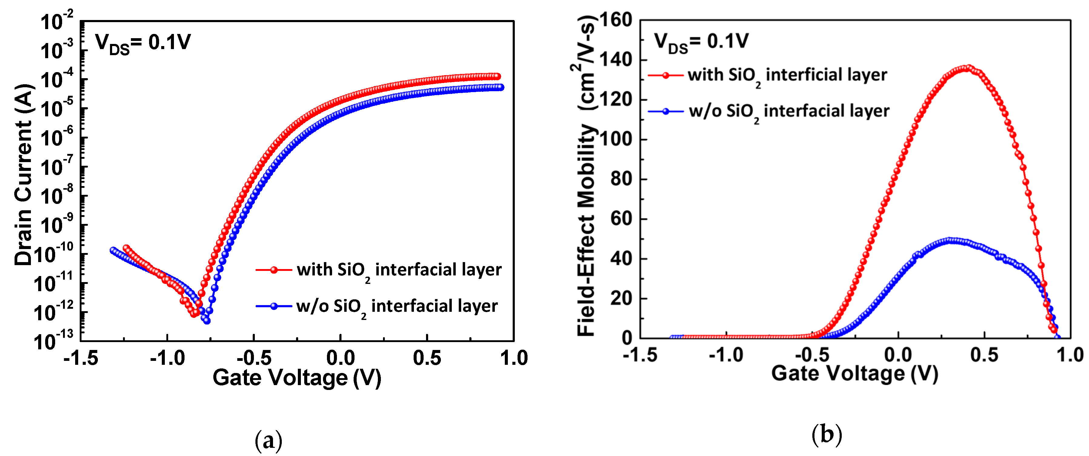
Figure 1a presents the drain-source current versus gate-source voltage (IDS-VGS) characteristics of the top-gate TFTs with and without the SiO2 interfacial layer between the SnO2 channel and the HfO2 gate dielectric. The devices, with and without the ultra-thin SiO2, exhibit good ION/IOFFs of 1.5 × 10⁸ and 1 × 10⁸, respectively, and sharp turn-on SS values of 108 and 117 mV/dec, respectively. The interface trap density (Dit) can be calculated from SS [29,30]:
where Cdep is the depletion capacitance. A Dit of 5.5 × 10¹² eV−1cm−2 is obtained, which is higher than the high-κ/silicon transistor. Further interface improvement can increase the SS and μFE.
Figure 1b depicts the μFE-VGS characteristics of these devices. The μFE was obtained by a standard method used in silicon IC from the trans-conductance (gm) at a small VDS of 0.1 V:
where WG, LG, and Cox are the gate width, gate length, and oxide capacitance, respectively. The Cox was obtained from the measured C-V characteristics divided by the area of the Ni/HfO2/SiO2/Al MIM device on the same chip. The SnO2 TFT with an SiO2 interfacial layer has a μFE as high as 136 cm2/Vs, which is significantly higher than the 49.3 cm2/Vs for the device without the SiO2 layer. This is the highest μFE value for top-gate TFTs made on an amorphous SiO2 substrate and processed at a temperature of ≤ 400 °C [21,22,23,24,25].
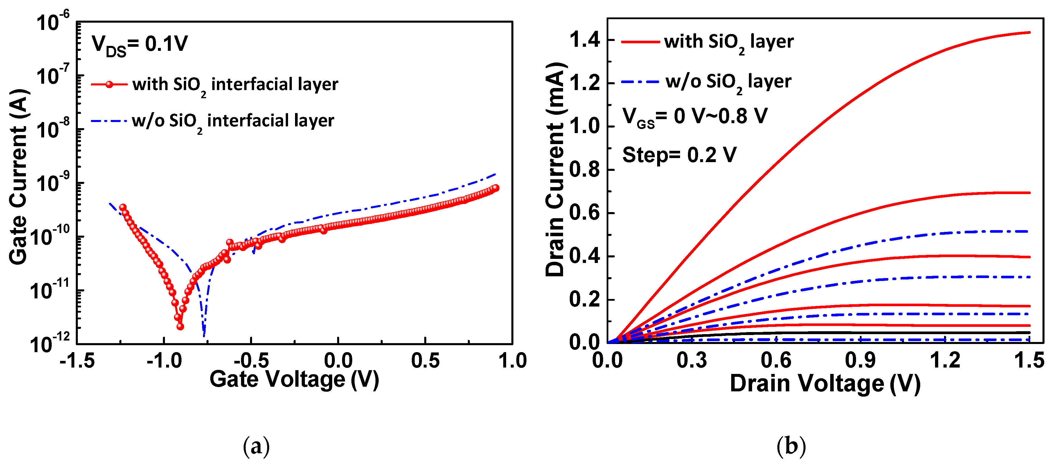
To understand the significantly better the IDS and μFE data for TFTs with an ultra-thin SiO2 layer, we further measured the gate-source current versus gate-source voltage (IGS-VGS) characteristics. As shown in Figure 2a, the gate leakage current does not demonstrate a significant difference between these two devices because the interfacial SiO2 layer was only 3 nm thick, and much thinner than the high-κ HfO2, which had a thickness of 50 nm. The IDS versus the drain-source voltage (IDS-VDS) characteristics are presented in Figure 2b. The TFT device with the ultra-thin SiO2 layer exhibits a higher IDS than the TFT without it, which is consistent with the IDS-VGS and μFE-VGS data presented in Figure 1a,b, because the higher IDS leads to a higher μFE value.
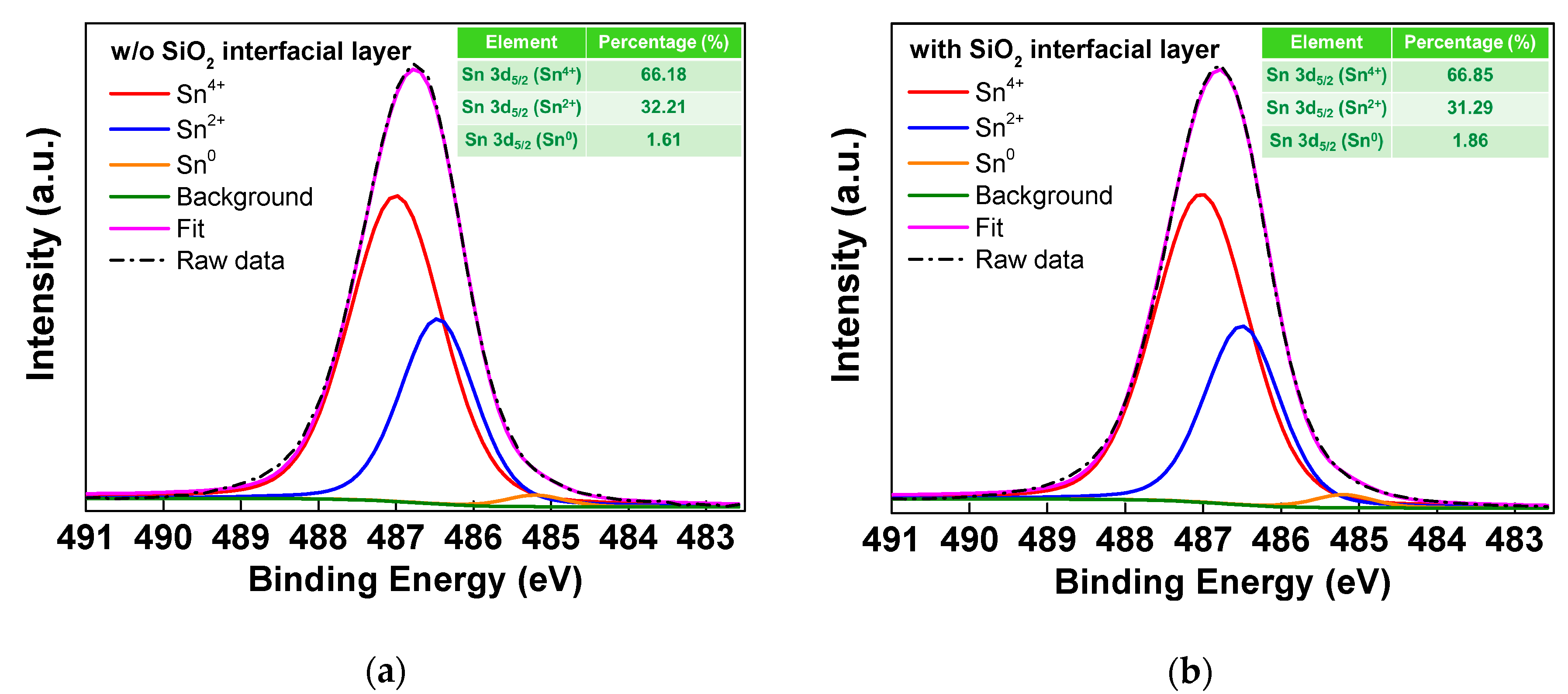
An XPS analysis was performed on both the HfO2/SiO2/SnO2 and the HfO2/SnO2 stacks. Before the analysis, both samples were sputter-etched from HfO2 to SnO2 at a slow rate of 0.1 nm/s. As shown in Figure 3, the Sn 3d5/2 spectrum of the SnOx layer is split into three peaks: Sn4+, Sn2+, and Sn0. The binding energies of the Sn4+, Sn2+, and Sn0 peaks were 487, 486.5, and 485.2 eV, respectively. The intensity of Sn2+ is related to the p-type SnO TFT [18]. By contrast, Sn4+ conducts electrons for n-type TFTs [11,12,13,14,15,16]. As the results obtained using XPS analysis do not indicate obvious differences between these two samples, the inserted SiO2 interfacial layer has little effect on the chemical composition of the SnOx channel layer.
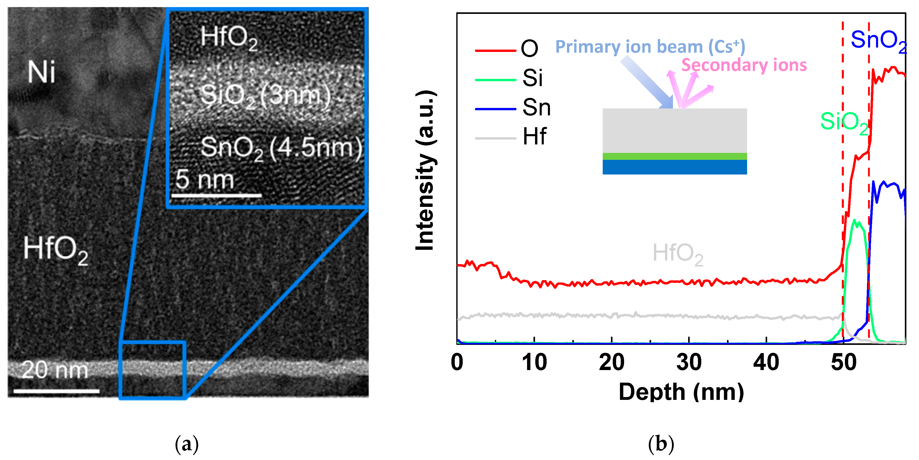
We further investigated the HfO2/SiO2/SnO2 stack through TEM and SIMS measurements. Figure 4a displays the cross-sectional TEM image of the SnO2 TFT with an SiO2 interfacial layer, where the thicknesses of HfO2, SiO2, and SnO2 were 50, 3, and 4.5 nm, respectively. The distributions of the Sn, Si, Hf, and O atoms in the gate stack and channel layer are depicted from the SIMS depth profiles in Figure 4b. An SiO2 interfacial layer was clearly observed in both the TEM and SIMS analyses.
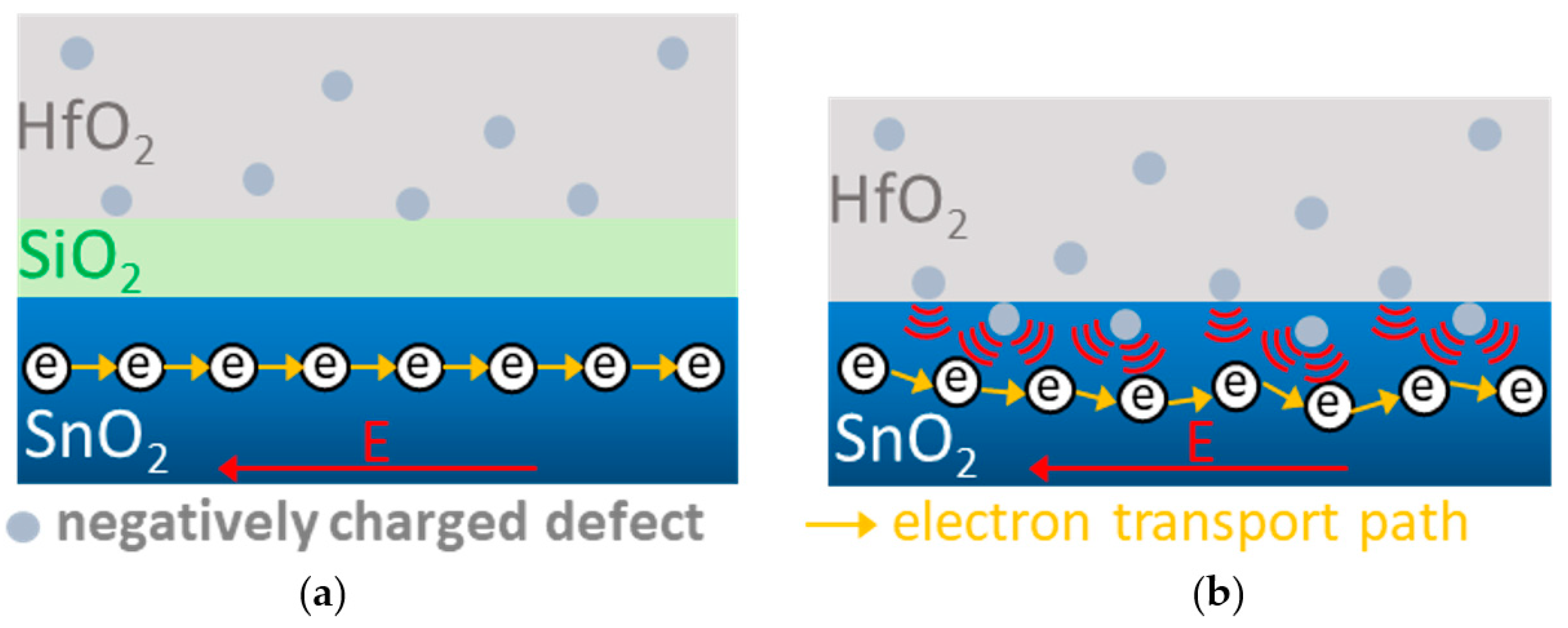
It is important to note that the extra SiO2 interfacial layer will increase the thickness of the gate dielectric slightly and theoretically lead to a slightly higher transistor threshold voltage (VTH) than the device without the SiO2 layer. However, the IDS-VGS characteristics of the SnO2 devices in Figure 1a display a contrary result. Thus, the increased VTH for the device without the interfacial SiO2 layer is due to the extra negative charges formed in HfO2. These negative charges may also exist in the HfO2/SnO2 interface because the interface charges are strongly related to SS [22], which improves with the extra SiO2 interfacial layer, as shown in Figure 1a. Further, such negative charges in the HfO2 and HfO2/SnO2 interfaces can cause electron scattering and degrade the mobility [31,32], as shown in Figure 1b. It is known that the high-κ gate dielectric has defects, especially when formed at low temperatures. The negative charges formed in the HfO2 and HfO2/SnO2 interfaces cause channel electron scattering and mobility degradation, which can be observed in the schematic diagrams illustrated in Figure 5a,b. The device with the SiO2 interfacial layer has less negative charge scattering in HfO2 and the interface because of the separation of the SiO2 layer, which results in a higher mobility and IDS.
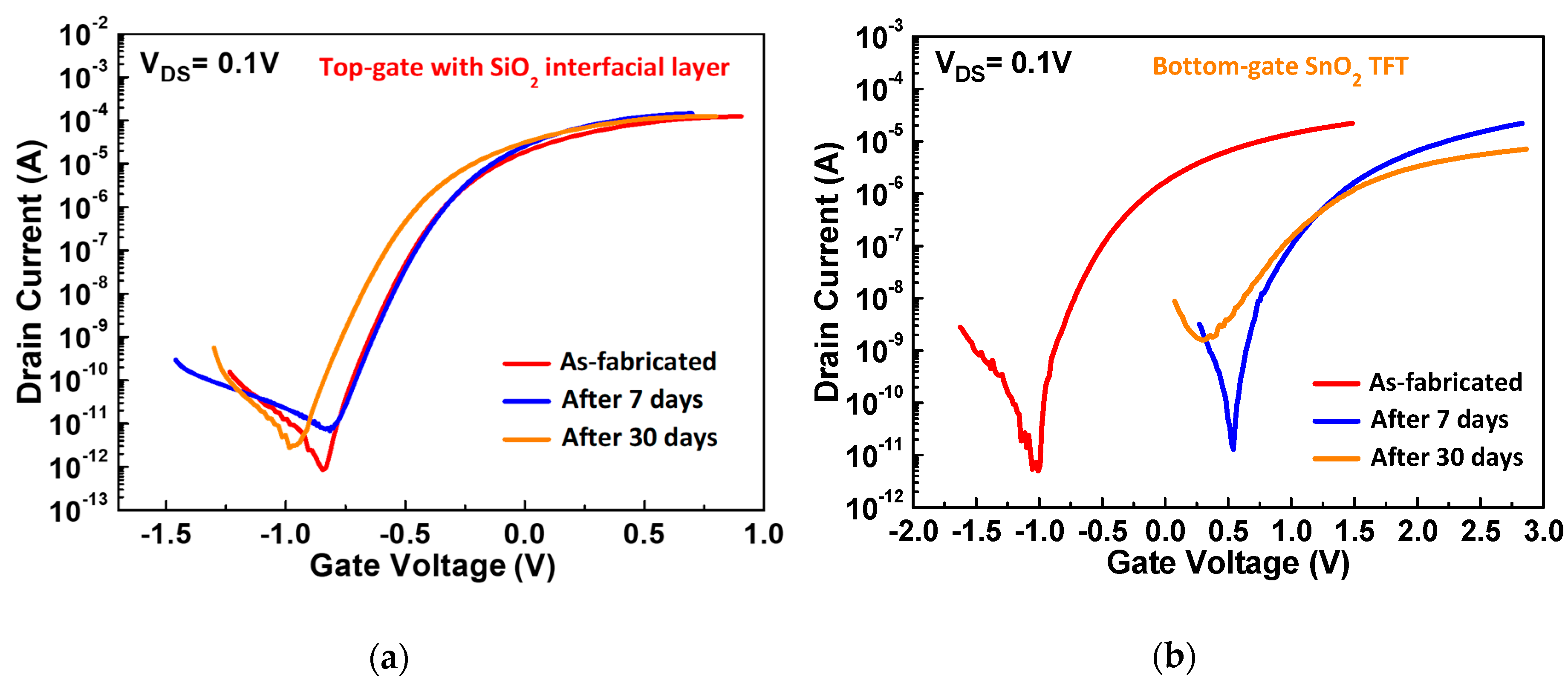
The moisture degradation of TFT devices is a significant issue for an IC. Figure 6 illustrates the IDS-VGS characteristics for the as-fabricated top-gate coplanar and bottom-gate staggered SnO2 TFTs in ambient air after 7 days and 30 days of exposure to air. The IDS-VGS characteristics of the bottom-gate SnO2 TFT are shifted as high as 1.5 V after 7 days of exposure, and the IOFF, SS, and ION further degrade significantly after 30 days of exposure to air. This is because the top SnO2 layer can react with H2O molecules in the air and form Sn-OH bonds [14,19,20], resulting in charged defects that lower the IDS and μFE. The penetration of OH- into the SnO2 could also form defects and lead to a higher IOFF by defect conduction [26]. In sharp contrast, only a slight VTH shift of −0.09 V was observed in the top-gate device because the gate dielectric HfO2 layer can behave as a passivation layer on the SnO2 channel layer. The slight VTH shift might be attributed to the intrinsic defects of the HfO2 layer and the charge trapping and de-trapping phenomena of those defects [33,34].
In Table 1, we summarize the important device characteristics and compare them with the published data on top-gate TFTs made on amorphous SiO2 substrates [21,22,23,24,25]. Our device with an ultra-thin channel thickness of 4.5 nm exhibits the highest μFE, a sharp SS for low-voltage operation, and a sufficiently large ION/IOFF, which are crucial for display, low-leakage DRAM access transistors, and monolithic 3D IC applications. Further improvement of μFE and SS may be reachable by using a thicker SnO2 layer than the 4.5 nm thickness and a Fin Field-Effect Transistor (FinFET) or gate-all-around structure, respectively.
4. Conclusions
An excellent device integrity was achieved for a top-gate TFT made on an amorphous SiO2 substrate using a low process temperature of 350 °C with a high μFE of 136 cm2/Vs, a sharp SS of 108 mV/dec for low-voltage operations, and a sufficiently large ION/IOFF of 1.5 × 10⁸. Such a top-gate structure is preferred for monolithic IC as compared to bottom-gate devices. In addition, a much better resistance to moisture can be achieved than in the bottom-gate device without passivation. Such a superb device performance is strongly related to the inserted ultra-thin SiO2 layer between the HfO2 and SnO2. The outstanding device performance with top-gate structure is a crucial technology for future-generation high-resolution displays, low-leakage DRAM access transistors, and monolithic 3D brain-mimicking ICs.
Author Contributions
Conceptualization, T.J.Y. and A.C.; supervision, A.C.; co-supervision, V.G. All authors have read and agreed to the published version of the manuscript.
Funding
This research was funded by Ministry of Science and Technology of Taiwan, project no. 107-2221-E-009-092-MY3.
Acknowledgments
We would also like to thank S.F. Liu for assisting with the device fabrication during his Master’s degree study.
Conflicts of Interest
The authors declare no conflict of interest.
References
- Klasens, H.A.; Koelmans, H. A tin oxide field-effect transistor. Solid State Electron. 1964, 7, 701–702. [Google Scholar] [CrossRef]
- Kwon, J.Y.; Son, K.S.; Jung, J.S.; Kim, T.S.; Ryu, A.K.; Park, K.B.; Yoo, B.W.; Kim, J.W.; Lee, Y.G.; Park, K.C.; et al. Bottom-gate Gallium Indium Zinc Oxide thin-film transistor array for high-resolution AMOLED display. IEEE Electron. Device Lett. 2008, 29, 1309–1311. [Google Scholar] [CrossRef]
- Xu, H.; Luo, D.; Li, M.; Xu, M.; Zou, J.; Tao, H.; Lan, L.; Wang, L.; Peng, J.; Cao, Y. A flexible AMOLED display on the PEN substrate driven by oxide thin-film transistors using anodized aluminium oxide as dielectric. J. Mater. Chem. C 2014, 2, 1255–1259. [Google Scholar] [CrossRef]
- Fortunato, E.; Barquinha, P.; Martins, R. Oxide semiconductor thin-film transistors: A review of recent advances. Adv. Mater. 2012, 24, 2945–2986. [Google Scholar] [CrossRef]
- Nomura, K.; Ohta, H.; Takagi, A.; Kamiya, T.; Hirano, M.; Hosono, H. Room-temperature fabrication of transparent flexible thin-film transistors using amorphous oxide semiconductors. Nature 2004, 432, 488–492. [Google Scholar] [CrossRef]
- Sekitani, T.; Zschieschang, U.; Klauk, H.; Someya, T. Flexible organic transistors and circuits with extreme bending stability. Nat. Mater. 2010, 9, 1015–1022. [Google Scholar] [CrossRef]
- Su, N.C.; Wang, S.J.; Huang, C.C.; Chen, Y.H.; Huang, H.Y.; Chiang, C.K.; Chin, A. Low-voltage-driven flexible InGaZnO thin-film transistor with small subthreshold swing. IEEE Electron. Device Lett. 2010, 31, 680–682. [Google Scholar]
- Zan, H.W.; Li, C.H.; Yeh, C.C.; Dai, M.Z.; Meng, H.F.; Tsai, C.C. Room-temperature-operated sensitive hybrid gas sensor based on amorphous indium gallium zinc oxide thin-film transistors. Appl. Phys. Lett. 2011, 98, 253503. [Google Scholar] [CrossRef] [Green Version]
- Kim, K.S.; Ahn, C.H.; Jung, S.H.; Cho, S.W.; Cho, H.K. Toward adequate operation of amorphous oxide thin-film transistors for low-concentration gas detection. ACS Appl. Mater. Interfaces 2018, 10, 10185–10193. [Google Scholar] [CrossRef]
- Liao, L.; Zhang, Z.; Yan, B.; Zheng, Z.; Bao, Q.L.; Wu, T.; Li, C.M.; Shen, Z.X.; Zhang, J.X.; Gong, H.; et al. Multifunctional CuO nanowire devices: P-type field effect transistors and CO gas sensors. Nanotechnology 2009, 20, 085203. [Google Scholar] [CrossRef] [Green Version]
- Shih, C.W.; Chin, A.; Lu, C.F.; Yi, S.H. Extremely high mobility ultra-thin metal-oxide with ns2np2 configuration. Int. Electron. Devices Meeting (IEDM) Technol. Dig. 2015, 145–148. [Google Scholar] [CrossRef]
- Chin, A.; Yen, T.J.; Shih, C.W.; Chen, Y.D. High mobility metal-oxide devices for display SoP and 3D brain-mimicking IC. Proc. Int. Disp. Workshops 2019, 26, 455–457. [Google Scholar] [CrossRef]
- Chin, A.; Chen, Y.D. Technologies toward three-dimensional brain-mimicking IC architecture. In Proceedings of the 2019 Electron Devices Technology and Manufacturing Conference (EDTM), Singapore, 12–15 March 2019; pp. 472–474. [Google Scholar]
- Shih, C.W.; Chin, A. Remarkably High mobility thin-film transistor on flexible substrate by novel passivation material. Sci. Rep. 2017, 7, 1147. [Google Scholar] [CrossRef] [PubMed] [Green Version]
- Shih, C.W.; Chin, A.; Lu, C.F.; Su, W.F. Remarkably high mobility ultra-thin-film metal-oxide transistor with strongly overlapped orbitals. Sci. Rep. 2016, 6, 19023. [Google Scholar] [CrossRef] [Green Version]
- Shih, C.W.; Yen, T.J.; Chin, A.; Lu, C.F.; Su, W.F. Low-temperature processed tin oxide transistor with ultraviolet irradiation. IEEE Electron Device Lett. 2019, 40, 909–912. [Google Scholar] [CrossRef]
- Shih, C.W.; Chin, A. New material transistor with record-high field-effect mobility among wide-band-gap semiconductors. ACS Appl. Mater. Interfaces 2016, 8, 19187–19191. [Google Scholar] [CrossRef] [PubMed] [Green Version]
- Shih, C.W.; Chin, A.; Lu, C.F.; Su, W.F. Remarkably high hole mobility metal-oxide thin-film transistors. Sci. Rep. 2018, 8, 889. [Google Scholar] [CrossRef] [Green Version]
- Yoo, D.Y.; Chong, E.; Kim, D.H.; Ju, B.K.; Lee, S.Y. Effect of magnesium oxide passivation on the performance of amorphous indium–gallium–zinc-oxide thin film transistors. Thin Solid Film 2012, 520, 3783–3786. [Google Scholar] [CrossRef]
- Chowdhury, M.D.H.; Mativenga, M.; Um, J.G.; Mruthyunjaya, R.K.; Heiler, G.N.; Tredwell, T.J.; Jang, J. Effect of SiO2 and SiO2/SiNx passivation on the stability of amorphous indium–gallium zinc-oxide thin-film transistors under high humidity. IEEE Trans. Electron Devices 2015, 62, 869–874. [Google Scholar] [CrossRef]
- Han, L.; Huang, Y.; Sturm, J.C.; Wagner, S. Self-aligned top-gate coplanar a-Si:H thin-film transistors with a SiO2–Silicone hybrid gate dielectric. IEEE Electron Device Lett. 2011, 32, 36–38. [Google Scholar] [CrossRef]
- Hung, B.F.; Chiang, K.C.; Huang, C.C.; Chin, A.; McAlister, S.P. High-performance poly-silicon TFTs incorporating LaAlO3 as the gate dielectric. IEEE Electron Device Lett. 2005, 26, 384–386. [Google Scholar] [CrossRef]
- Zhang, S.; Shao, Y. Technology issues for self-aligned top-gate amorphous metal oxide thin-film transistors. In Proceedings of the IEEE International Conference on Electron Devices and Solid State Circuits, Shenzhen, China, 6–8 June 2018. [Google Scholar]
- Deng, S. Gate Insulator engineering in top-gated indium-tin-oxide-stabilized ZnO thin-film transistors. IEEE Electron. Device Lett. 2019, 40, 1104–1107. [Google Scholar] [CrossRef]
- Lim, D.; Jeon, Y.; Kim, M.; Kim, Y.; Kim, S. Electrical characteristics of SnO2 thin-film transistors fabricated on bendable substrates using reactive magnetron sputtering. J. Nanosci. Nanotechnol. 2016, 16, 11697–11700. [Google Scholar] [CrossRef]
- Saha, J.K.; Bukke, R.N.; Mude, N.N.; Jang, J. Remarkable Stability Improvement of ZnO TFT with Al2O3 Gate Insulator by Yttrium Passivation with Spray Pyrolysis. Nanomaterials 2020, 10, 976. [Google Scholar] [CrossRef]
- Zhu, S.; Chen, J.; Li, M.-F.; Lee, S.J.; Singh, J.; Zhu, C.X.; Du, A.; Tung, C.H.; Chin, A.; Kwong, D.L. N-type Schottky barrier source/drain MOSFET using ytterbium silicide. IEEE Electron Device Lett. 2004, 25, 565–567. [Google Scholar] [CrossRef]
- Zhu, S.; Yu, H.Y.; Whang, S.J.; Chen, J.H.; Shen, C.; Zhu, C.; Lee, S.J.; Li, M.F.; Chan, D.S.H.; Yoo, W.J.; et al. Schottky-barrier S/D MOSFETs with high-k gate dielectrics and metal gate electrode. IEEE Electron Device Lett. 2004, 25, 268–270. [Google Scholar] [CrossRef]
- Chang, M.F.; Lee, P.T.; McAlister, S.P.; Chin, A. Low sub-threshold swing HfLaO/Pentacene organic thin film transistors. IEEE Electron Device Lett. 2008, 29, 215–217. [Google Scholar] [CrossRef]
- Kim, M.S.; Kim, H.T.; Chi, S.S.; Kim, T.E.; Shin, H.T.; Kang, K.W.; Park, H.S.; Kim, D.J.; Min, K.S.; Kang, D.W.; et al. Distribution of interface states in MOS systems extracted by the subthreshold current in MOSFETs under optical illumination. J. Korean Phys. Soc. 2003, 43, 873–878. [Google Scholar] [CrossRef]
- Fischetti, M.V.; Neumayer, D.A.; Cartier, E.A. Effective electron mobility in Si inversion layers in metal-oxide-semiconductor systems with a high-kappa insulator: The role of remote phonon scattering. J. Appl. Phys. 2001, 90, 4587–4608. [Google Scholar] [CrossRef]
- Maitra, K. Impact of metal gates on remote phonon scattering in titanium nitride/hafnium dioxide n-channel metal–oxide–semiconductor field effect transistors–low temperature electron mobility study. J. Appl. Phys. 2007, 102, 114507. [Google Scholar] [CrossRef]
- Zafar, S.; Callegari, A.; Gusev, E.; Fischetti, M.V. Charge trapping related threshold voltage instabilities in high permittivity gate dielectric stacks. J. Appl. Phys. 2003, 93, 9298–9303. [Google Scholar] [CrossRef]
- Lee, B.H. Intrinsic characteristics of high-k devices and implications of fast transient charging effects (FTCE). In Proceedings of the IEDM Technical Digest. IEEE International Electron Devices Meeting, San Francisco, CA, USA, 13–15 December 2004; pp. 859–862. [Google Scholar]
Figure 1.
(a) IDS-VGS and (b) μFE-VGS characteristics of the top-gate SnO2 TFTs with and without an SiO2 interfacial layer.
Figure 1.
(a) IDS-VGS and (b) μFE-VGS characteristics of the top-gate SnO2 TFTs with and without an SiO2 interfacial layer.

Figure 2.
(a) IGS-VGS and (b) IDS-VDS characteristics of the top-gate SnO2 with and without an SiO2 interfacial layer.
Figure 2.
(a) IGS-VGS and (b) IDS-VDS characteristics of the top-gate SnO2 with and without an SiO2 interfacial layer.

Figure 3.
The XPS spectra of Sn 3d5/2 in the SnO2 layer of the TFT devices (a) without and (b) with an SiO2 interfacial layer.
Figure 3.
The XPS spectra of Sn 3d5/2 in the SnO2 layer of the TFT devices (a) without and (b) with an SiO2 interfacial layer.

Figure 4.
(a) The cross-sectional TEM image and (b) SIMS depth profiles of the SnO2 TFT with an SiO2 interfacial layer.
Figure 4.
(a) The cross-sectional TEM image and (b) SIMS depth profiles of the SnO2 TFT with an SiO2 interfacial layer.

Figure 5.
The schematic diagrams for electron transport in (a) with (b) without an SiO2 interfacial layer. Negative charges formed in HfO2 for a device without an SiO2 layer will increase the electron scattering and lower the mobility.
Figure 5.
The schematic diagrams for electron transport in (a) with (b) without an SiO2 interfacial layer. Negative charges formed in HfO2 for a device without an SiO2 layer will increase the electron scattering and lower the mobility.

Figure 6.
The IDS-VGS characteristics of the (a) top-gate and (b) bottom-gate SnO2 TFT devices measured as-fabricated after 7 days and after 30 days of exposure to ambient air.
Figure 6.
The IDS-VGS characteristics of the (a) top-gate and (b) bottom-gate SnO2 TFT devices measured as-fabricated after 7 days and after 30 days of exposure to ambient air.


Table 1.
Important device performance comparison of various top-gate TFT devices on SiO2 substrate.
| Channel Materials | Channel Thickness (nm) | μFE (cm2/V·s) @VDS(V) | ION/IOFF | SS (mV/Decade) |
|---|---|---|---|---|
| a-Si [21] | 100 | 0.9 @ 0.1 | 105 | 380 |
| Poly-Si [22] | 100 | 40 @ 0.1 | 1.5 × 10⁶ | 310 |
| IGZO [23] | 40 | 11.44 @ 10 | 108 | 360 |
| ZnO [24] | 50 | 16.8 @ 0.1 | 2.4 × 10⁹ | 102 |
| SnO2 [25] | 30 | 4.43 @ 1 | 4.19 × 10⁶ | 300 |
| SnO2 this work | 4.5 | 136 @ 0.1 | 1.5 × 10⁸ | 108 |
Publisher’s Note: MDPI stays neutral with regard to jurisdictional claims in published maps and institutional affiliations. |
© 2020 by the authors. Licensee MDPI, Basel, Switzerland. This article is an open access article distributed under the terms and conditions of the Creative Commons Attribution (CC BY) license (http://creativecommons.org/licenses/by/4.0/).
Share and Cite
MDPI and ACS Style
Yen, T.J.; Chin, A.; Gritsenko, V. High-Performance Top-Gate Thin-Film Transistor with an Ultra-Thin Channel Layer. Nanomaterials 2020, 10, 2145. https://0-doi-org.brum.beds.ac.uk/10.3390/nano10112145
AMA Style
Yen TJ, Chin A, Gritsenko V. High-Performance Top-Gate Thin-Film Transistor with an Ultra-Thin Channel Layer. Nanomaterials. 2020; 10(11):2145. https://0-doi-org.brum.beds.ac.uk/10.3390/nano10112145
Chicago/Turabian StyleYen, Te Jui, Albert Chin, and Vladimir Gritsenko. 2020. "High-Performance Top-Gate Thin-Film Transistor with an Ultra-Thin Channel Layer" Nanomaterials 10, no. 11: 2145. https://0-doi-org.brum.beds.ac.uk/10.3390/nano10112145
Note that from the first issue of 2016, this journal uses article numbers instead of page numbers. See further details here.