Stable and Multilevel Data Storage Resistive Switching of Organic Bulk Heterojunction


 and
and 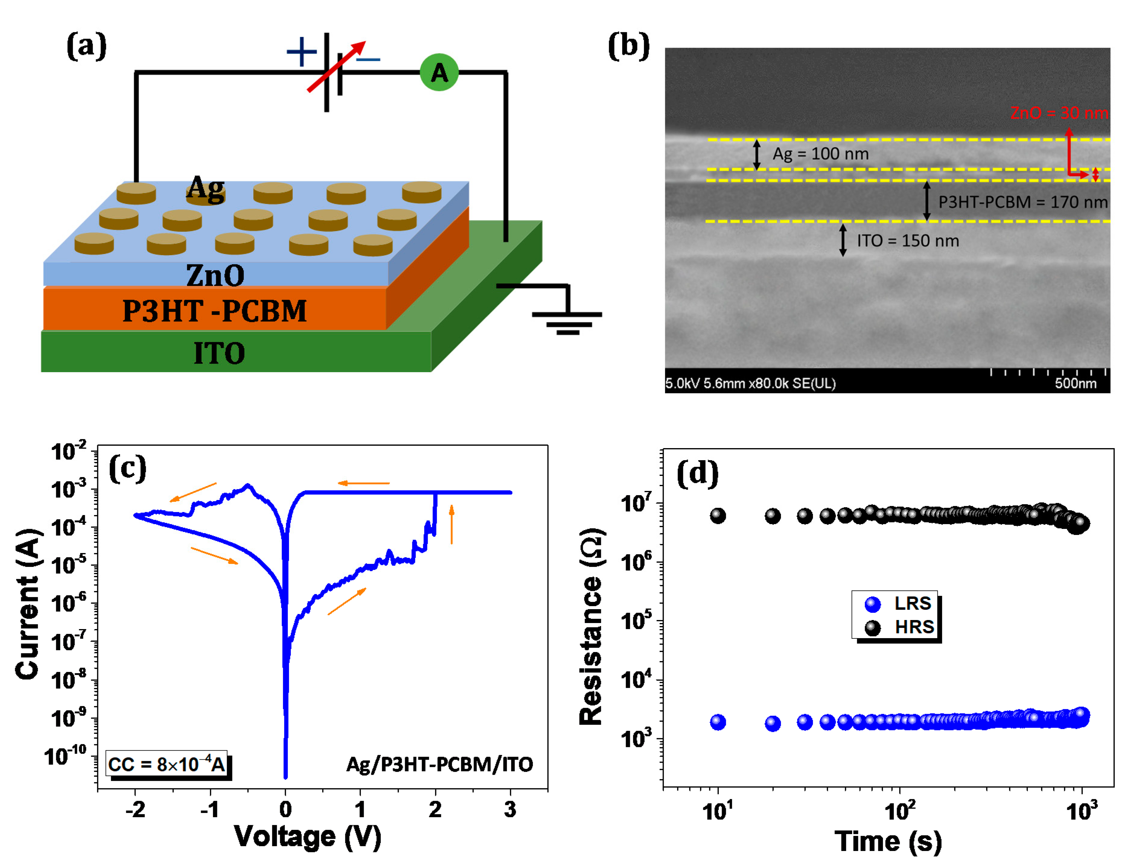
Abstract
:1. Introduction
2. Materials and Methods
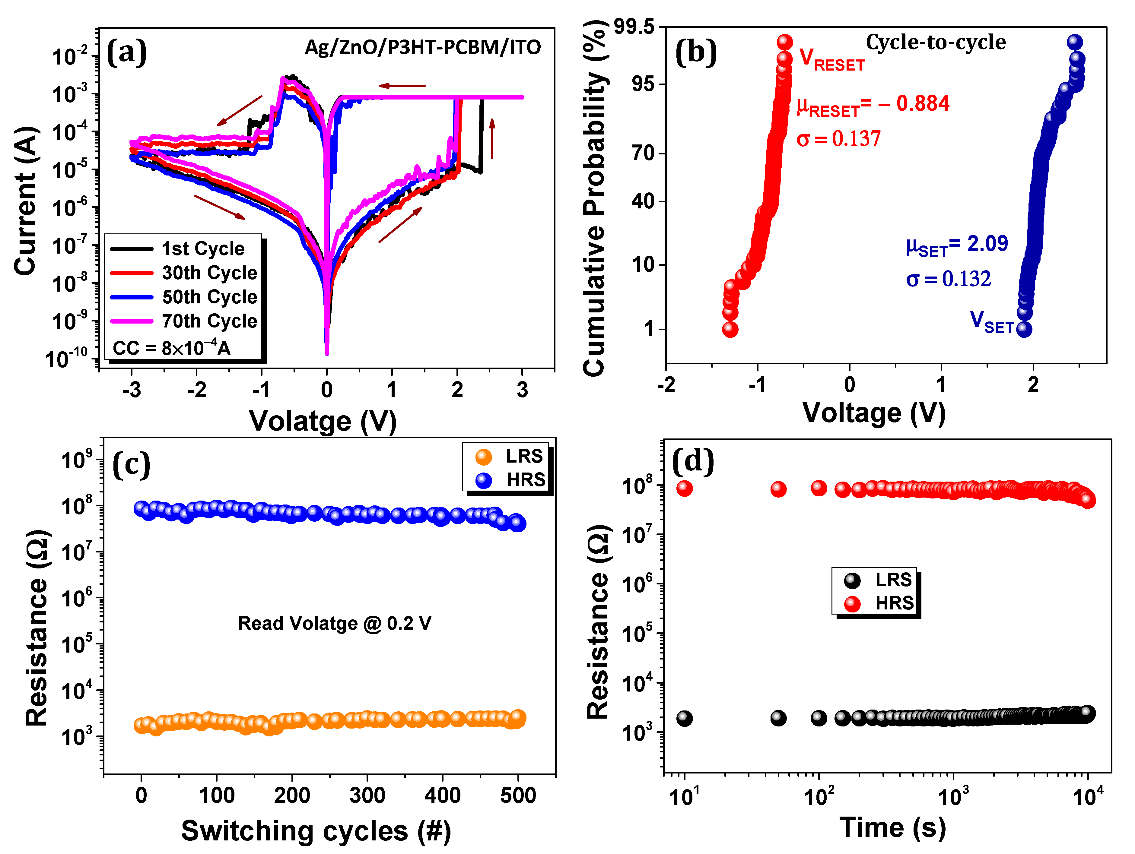
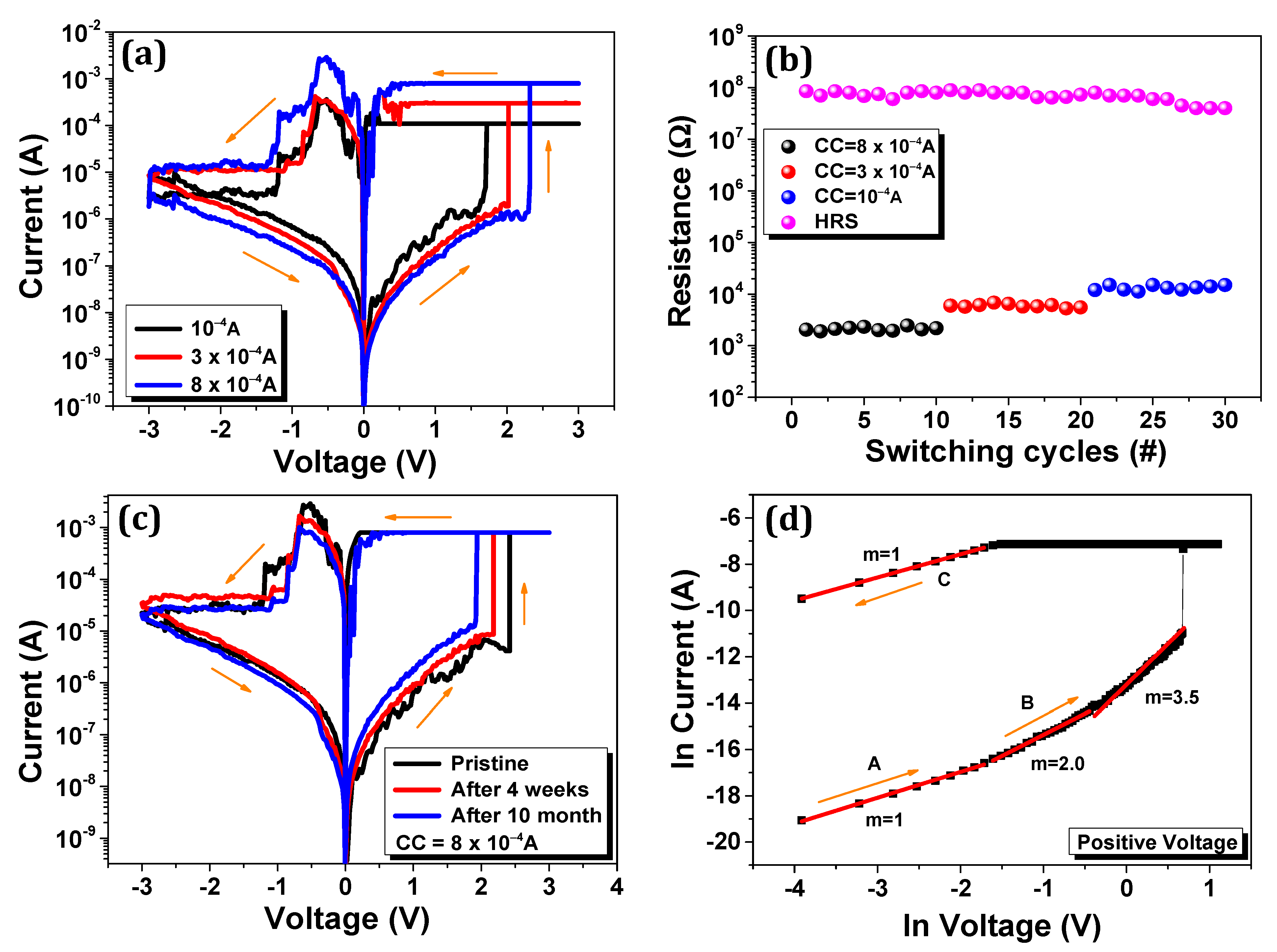
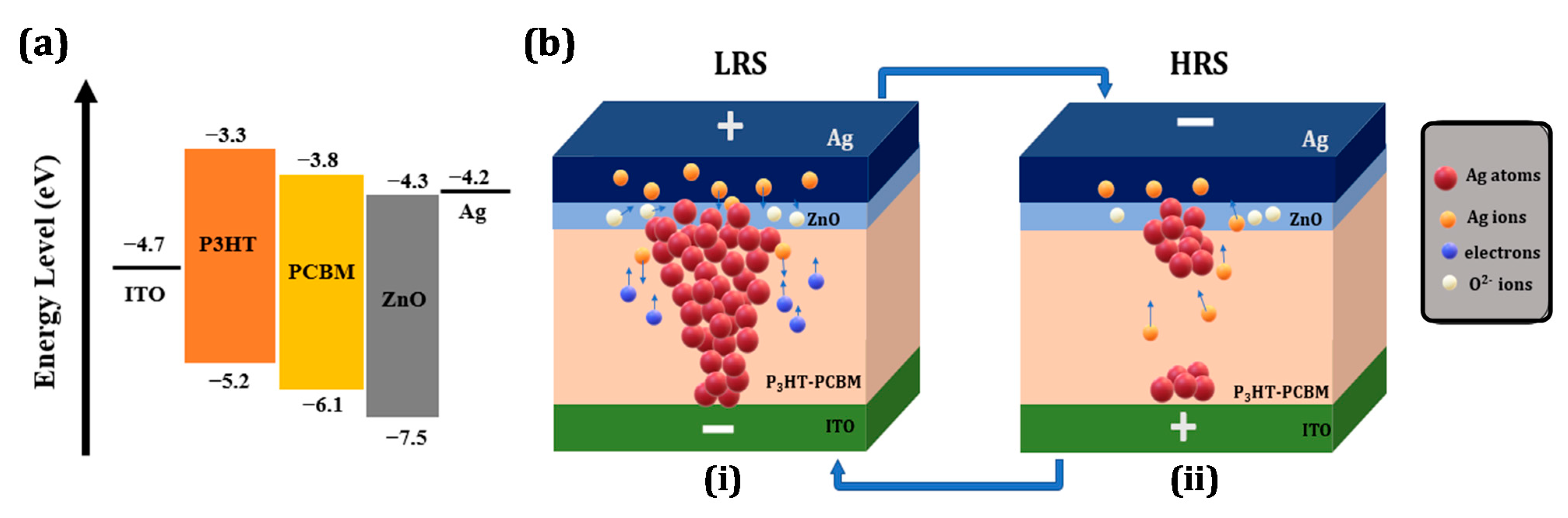
3. Results and Discussion
4. Conclusions
Supplementary Materials
Author Contributions
Funding
Data Availability Statement
Acknowledgments
Conflicts of Interest
References
- Cho, B.; Song, S.; Ji, Y.; Choi, H.-G.; Ko, H.C.; Lee, J.-S.; Jung, G.-Y.; Lee, T. Demonstration of Addressable Organic Resistive Memory Utilizing a PC-Interface Memory Cell Tester. IEEE Electron Device Lett. 2012, 34, 51–53. [Google Scholar] [CrossRef]
- Kim, Y.; Yoo, D.; Jang, J.; Song, Y.; Jeong, H.; Cho, K.; Hwang, W.-T.; Lee, W.; Kim, T.-W.; Lee, T. Characterization of PI:PCBM organic nonvolatile resistive memory devices under thermal stress. Org. Electron. 2016, 33, 48–54. [Google Scholar] [CrossRef]
- Kim, H.; Kumar, S.; Kim, O.J.; Iyer, S.S.K.; Kim, D.-K. Ag back electrode bonding process for inverted organic solar cells. J. Alloy. Compd. 2019, 777, 294–301. [Google Scholar] [CrossRef]
- Rehman, S.; Kim, H.; Khan, M.F.; Hur, J.-H.; Eom, J.; Kim, D.-K. Tunable resistive switching of vertical ReSe2/graphene hetero-structure enabled by Schottky barrier height and DUV light. J. Alloys Compd. 2020, 855, 157310. [Google Scholar] [CrossRef]
- Sun, Y.; Wen, D.; Sun, F. Influence of blending ratio on resistive switching effect in donor-acceptor type composite of PCBM and PVK-based memory devices. Org. Electron. 2019, 65, 141–149. [Google Scholar] [CrossRef]
- Lian, S.-L.; Liu, C.; Chen, W.-C. Conjugated Fluorene Based Rod–Coil Block Copolymers and Their PCBM Composites for Resistive Memory Switching Devices. ACS Appl. Mater. Interfaces 2011, 3, 4504–4511. [Google Scholar] [CrossRef] [PubMed]
- Song, S.; Cho, B.; Kim, T.-W.; Ji, Y.; Jo, M.; Wang, G.; Choe, M.; Kahng, Y.H.; Hwang, H.; Lee, T. Three-Dimensional Integration of Organic Resistive Memory Devices. Adv. Mater. 2010, 22, 5048–5052. [Google Scholar] [CrossRef] [PubMed]
- Rehman, S.; Kim, H.; Khan, M.F.; Hur, J.-H.; Lee, A.D.; Kim, D.-K. Tuning of ionic mobility to improve the resistive switching behavior of Zn-doped CeO2. Sci. Rep. 2019, 9, 1–10. [Google Scholar] [CrossRef] [PubMed] [Green Version]
- Sun, Y.; Wen, D.; Bai, X. Nonvolatile ternary resistive switching memory devices based on the polymer composites containing zinc oxide nanoparticles. Phys. Chem. Chem. Phys. 2018, 20, 5771–5779. [Google Scholar] [CrossRef]
- Lv, W.; Wang, H.; Jia, L.; Tang, X.; Lin, C.; Yuwen, L. Tunable nonvolatile memory behaviors of PCBM–MoS2 2D nanocomposites through Surface deposition ratio control. ACS Appl. Mater. Interfaces 2018, 10, 6552–6559. [Google Scholar] [CrossRef]
- Huang, R.; Cai, Y.; Liu, Y.; Bai, W.; Kuang, Y.; Wang, Y. Resistive switching in organic memory devices for flexible applications. In Proceedings of the Book Resistive switching in Organic Memory Devices for Flexible Applications, Melbourne, Australia, 1–5 June 2014; pp. 838–841. [Google Scholar]
- Ali, S.; Bae, J.; Lee, C.H.; Shin, S.; Kobayashi, N.P. Ultra-low power non-volatile resistive crossbar memory based on pull up resistors. Org. Electron. 2017, 41, 73–78. [Google Scholar] [CrossRef]
- Quinteros, C.; Zazpe, R.; Marlasca, F.; Golmar, F.; Casanova, F.; Stoliar, P. HfO2 based memory devices with rectifying capabilities. J. Appl. Phys. 2014, 115, 024501. [Google Scholar] [CrossRef] [Green Version]
- Minnekhanov, A.; Emelyanov, A.; Lapkin, D.A.; Nikiruy, K.E.; Shvetsov, B.S.; Nesmelov, A.A.; Rylkov, V.V.; Demin, V.A.; Erokhin, V. Parylene based memristive devices with multilevel resistive switching for neuromorphic applications. Sci. Rep. 2019, 9, 1–9. [Google Scholar] [CrossRef] [PubMed]
- Matsukatova, A.N.; Emelyanov, A.V.; Minnekhanov, A.A.; Demin, V.A.; Rylkov, V.V.; Forsh, P.A.; Kashkarov, P.K. Second-Order Nanoscale Thermal Effects in Memristive Structures Based on Poly-p-Xylylene. JETP Lett. 2020, 112, 357–363. [Google Scholar] [CrossRef]
- Wu, C.; Kim, T.W.; Choi, H.Y.; Strukov, D.B.; Yang, J.J. Flexible three-dimensional artificial synapse networks with correlated learning and trainable memory capability. Nat. Commun. 2017, 8, 1–9. [Google Scholar] [CrossRef] [PubMed] [Green Version]
- Chen, Q.; Lin, M.; Wang, Z.; Zhao, X.; Cai, Y.; Qi, L.; Fang, Y.; Yang, Y.; He, M.; Huang, R. Low Power Parylene-Based Memristors with a Graphene Barrier Layer for Flexible Electronics Applications. Adv. Electron. Mater. 2019, 5, 1800852. [Google Scholar] [CrossRef]
- Zhang, H.; Zhao, X.; Huang, J.; Bai, J.; Hou, Y.; Wang, C. Bistable non-volatile resistive memory devices based on ZnO nanoparticles embedded in polyvinylpyrrolidone. RSC Adv. 2020, 10, 14662–14669. [Google Scholar] [CrossRef]
- Varun, I.; Bharti, D.; Mahato, A.K.; Raghuwanshi, V.; Tiwari, S.P. High-Performance Flexible Resistive RAM With PVP:GO Composite and Ultrathin HfO x Hybrid Bilayer. IEEE Trans. Electron Devices 2020, 67, 949–954. [Google Scholar] [CrossRef]
- Zhao, Y.; Sun, W.; Wang, M.; He, J.; Lu, J. Flexible Ternary Resistive Memory from Organic Bulk Heterojunction. Adv. Mater. Technol. 2019, 5, 1900681. [Google Scholar] [CrossRef]
- Gao, S.; Song, C.; Chen, C.; Zeng, F.; Pan, F. Dynamic Processes of Resistive Switching in Metallic Filament-Based Organic Memory Devices. J. Phys. Chem. C 2012, 116, 17955–17959. [Google Scholar] [CrossRef]
- Pawar, K.K.; Desai, D.V.; Bodake, S.M.; Patil, H.S.; More, S.M.; Nimbalkar, A.S.; Mali, S.S.; Hong, C.K.; Kim, S.; Patil, P.S.; et al. Highly reliable multilevel resistive switching in a nanoparticulated In2O3 thin-film memristive device. J. Phys. D: Appl. Phys. 2019, 52, 175306. [Google Scholar] [CrossRef]
- Deshpande, S.; Nair, V.V. Resistive switching of Al/Sol-Gel ZnO/Al devices for resistive random access memory applications. In Proceedings of the Book Resistive switching of Al/Sol-Gel ZnO/Al devices for resistive random access memory applications, Trivandrum, Kerala, India, 28–29 December 2009; pp. 471–473. [Google Scholar]
- Ren, S.; Dong, W.; Tang, H.; Tang, L.; Li, Z.; Sun, Q.; Yang, H.; Yang, Z.; Zhao, J. High-efficiency magnetic modulation in Ti/ZnO/Pt resistive random-access memory devices using amorphous zinc oxide film. Appl. Surf. Sci. 2019, 488, 92–97. [Google Scholar] [CrossRef]
- Ismail, M.; Talib, I.; Rana, A.M.; Akbar, T.; Jabeen, S.; Lee, J.; Kim, S. Effect of Bilayer CeO2−x/ZnO and ZnO/CeO2−x Heterostructures and Electroforming Polarity on Switching Properties of Non-volatile Memory. Nanoscale Res. Lett. 2018, 13, 318. [Google Scholar] [CrossRef] [PubMed]
- Wang, H.; Meng, F.; Cai, Y.; Zheng, L.; Li, Y.; Liu, Y.; Jiang, Y.; Wang, X.; Chen, X. Sericin for Resistance Switching Device with Multilevel Nonvolatile Memory. Adv. Mater. 2013, 25, 5498–5503. [Google Scholar] [CrossRef]
- Verbakel, F.; Meskers, S.C.J.; Janssen, R.A.J.; Gomes, H.L.; Cölle, M.; Büchel, M.; De Leeuw, D.M. Reproducible resistive switching in nonvolatile organic memories. Appl. Phys. Lett. 2007, 91, 192103. [Google Scholar] [CrossRef] [Green Version]
- Lee, W.; Kim, Y.; Song, Y.; Cho, K.; Yoo, D.; Ahn, H.; Kang, K.; Lee, T. Investigation of Time-Dependent Resistive Switching Behaviors of Unipolar Nonvolatile Organic Memory Devices. Adv. Funct. Mater. 2018, 28, 1801162. [Google Scholar] [CrossRef]
- Wu, Y.; Wei, Y.; Huang, Y.; Cao, F.; Yu, D.; Li, X.; Zeng, H. Capping CsPbBr3 with ZnO to improve performance and stability of perovskite memristors. Nano Res. 2017, 10, 1584–1594. [Google Scholar] [CrossRef]
- Rehman, M.M.; Yang, B.-S.; Yang, Y.-J.; Karimov, K.S.; Choi, K.H. Effect of device structure on the resistive switching characteristics of organic polymers fabricated through all printed technology. Curr. Appl. Phys. 2017, 17, 533–540. [Google Scholar] [CrossRef]
- Wang, T.Y.; Meng, J.L.; He, Z.Y.; Chen, L.; Zhu, H.; Sun, Q.Q.; Ding, S.J.; Zhang, D.W. Atomic layer deposited Hf0.5Zr0.5O2-based flexible memristor with short/long-term synaptic plasticity. Nanoscale Res. Lett. 2019, 14, 102. [Google Scholar] [CrossRef] [Green Version]
- Ji, Y.; Zeigler, D.F.; Lee, D.S.; Choi, H.; Jen, A.K.-Y.; Ko, H.C.; Kim, T.-W. Flexible and twistable non-volatile memory cell array with all-organic one diode–one resistor architecture. Nat. Commun. 2013, 4, 2707. [Google Scholar] [CrossRef] [Green Version]
- Gao, S.; Zeng, F.; Chen, C.; Tang, G.; Lin, Y.; Zheng, Z.; Song, C.; Pan, F. Conductance quantization in a Ag filament-based polymer resistive memory. Nanotechnology 2013, 24, 335201. [Google Scholar] [CrossRef] [PubMed]
- Liu, J.; Yin, Z.; Cao, X.; Zhao, F.; Lin, A.; Xie, L.; Fan, Q.; Boey, F.; Zhang, H.; Li, Y.-H. Bulk Heterojunction Polymer Memory Devices with Reduced Graphene Oxide as Electrodes. ACS Nano 2010, 4, 3987–3992. [Google Scholar] [CrossRef] [PubMed]
- Jin, Z.; Liu, G.; Wang, J. Organic nonvolatile resistive memory devices based on thermally deposited Au nanoparticle. AIP Adv. 2013, 3, 052113. [Google Scholar] [CrossRef]
- Khan, M.U.; Hassan, G.; Raza, M.A.; Bae, J.; Kobayashi, N.P. Schottky diode based resistive switching device based on ZnO/PEDOT: PSS heterojunction to reduce sneak current problem. J. Mater. Sci. Mater. Electron. 2019, 30, 4607–4617. [Google Scholar] [CrossRef]
- Oh, S.H.; Heo, S.J.; Yang, J.S.; Kim, H.J. Effects of ZnO nanoparticles on P3HT: PCBM organic solar cells with DMF-modulated PEDOT: PSS buffer layers. ACS Appl. Mater. Interfaces 2013, 5, 11530–11534. [Google Scholar] [CrossRef] [PubMed]
- Bejtka, K.; Milano, G.; Ricciardi, C.; Pirri, C.F.; Porro, S. TEM nano-structural investigation of Ag conductive filaments in polycrystalline ZnO-based resistive switching devices. ACS Appl. Mater. Interfaces 2020, 12, 29451–29460. [Google Scholar] [PubMed]
- Aziz, J.; Kim, H.; Rehman, S.; Khan, M.F.; Kim, D.-K. Chemical Nature of Electrode and the Switching Response of RF-Sputtered NbOx Films. Nanomaterials 2020, 10, 2164. [Google Scholar] [CrossRef]


Publisher’s Note: MDPI stays neutral with regard to jurisdictional claims in published maps and institutional affiliations. |
© 2021 by the authors. Licensee MDPI, Basel, Switzerland. This article is an open access article distributed under the terms and conditions of the Creative Commons Attribution (CC BY) license (http://creativecommons.org/licenses/by/4.0/).
Share and Cite
Patil, H.; Kim, H.; Rehman, S.; Kadam, K.D.; Aziz, J.; Khan, M.F.; Kim, D.-k. Stable and Multilevel Data Storage Resistive Switching of Organic Bulk Heterojunction. Nanomaterials 2021, 11, 359. https://0-doi-org.brum.beds.ac.uk/10.3390/nano11020359
Patil H, Kim H, Rehman S, Kadam KD, Aziz J, Khan MF, Kim D-k. Stable and Multilevel Data Storage Resistive Switching of Organic Bulk Heterojunction. Nanomaterials. 2021; 11(2):359. https://0-doi-org.brum.beds.ac.uk/10.3390/nano11020359
Chicago/Turabian StylePatil, Harshada, Honggyun Kim, Shania Rehman, Kalyani D. Kadam, Jamal Aziz, Muhammad Farooq Khan, and Deok-kee Kim. 2021. "Stable and Multilevel Data Storage Resistive Switching of Organic Bulk Heterojunction" Nanomaterials 11, no. 2: 359. https://0-doi-org.brum.beds.ac.uk/10.3390/nano11020359