
Plasma Assisted Reduction of Graphene Oxide Films

Institute of High-Frequency and Semiconductor System Technologies, Technische Universität Berlin, HFT 5-2, Einsteinufer 25, 10587 Berlin, Germany
*
Author to whom correspondence should be addressed.
Nanomaterials 2021, 11(2), 382; https://0-doi-org.brum.beds.ac.uk/10.3390/nano11020382
Submission received: 8 January 2021
/
Revised: 25 January 2021
/
Accepted: 28 January 2021
/
Published: 3 February 2021
(This article belongs to the Special Issue Physics and Chemistry of Graphene: From Fundamentals to Applications)
Abstract
:The past decade has seen enormous efforts in the investigation and development of reduced graphene oxide (GO) and its applications. Reduced graphene oxide (rGO) derived from GO is known to have relatively inferior electronic characteristics when compared to pristine graphene. Yet, it has its significance attributed to high-yield production from inexpensive graphite, ease of fabrication with solution processing, and thus a high potential for large-scale applications and commercialization. Amongst several available approaches for GO reduction, the mature use of plasma technologies is noteworthy. Plasma technologies credited with unique merits are well established in the field of nanotechnology and find applications across several fields. The use of plasma techniques for GO development could speed up the pathway to commercialization. In this report, we review the state-of-the-art status of plasma techniques used for the reduction of GO-films. The strength of various techniques is highlighted with a summary of the main findings in the literature. An analysis is included through the prism of chemistry and plasma physics.
1. Introduction
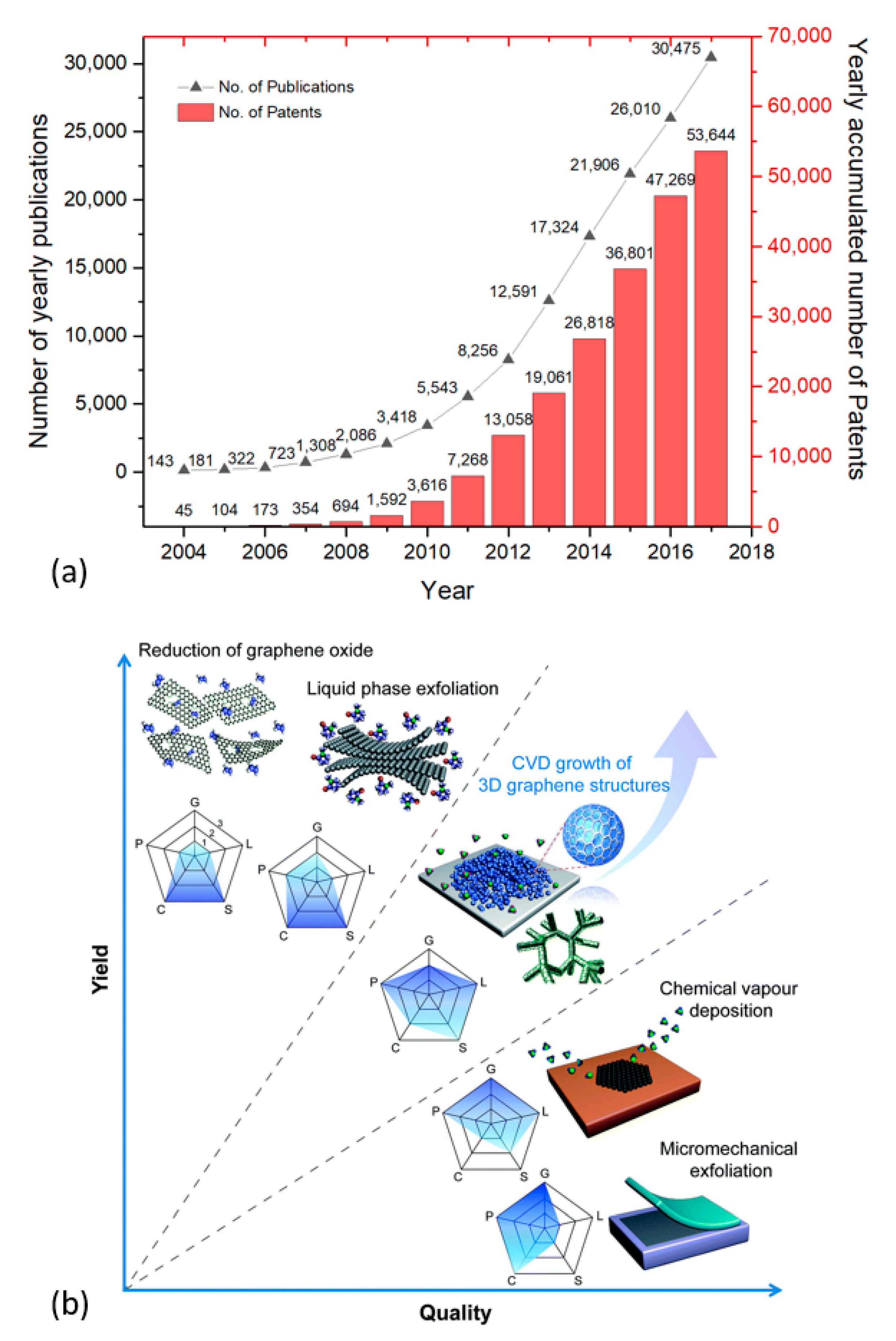
The term “graphene” was coined by Boehm et al. in 1985, which refers to a two-dimensional single layer of carbon atoms in a honeycomb lattice [1]. A. Geim and K. Novoselov exfoliated graphene for the first time in the year 2004, which consequently earned them a Physics Nobel prize in 2010. Even before its discovery and eventually gaining the “wonder material” nickname [2], graphene was known to scientists and used in theoretical studies dating back to 1947 [3,4,5,6,7,8,9]. Following the discovery, graphene has gained a lot of attention from the scientific community across various disciplines (Figure 1a). This can be credited to its remarkable electrical, optical, thermal, and mechanical properties [9,10,11]. Additionally, it possesses complete non-permeability to all standard gases [12] and the ability to be chemically functionalized [13,14].
Figure 1b presents schematic illustrations of the common production methods of graphene. A detailed account of various production and processing techniques of graphene and related materials can be found in the literature [15,16,17,18]. Methods such as mechanical exfoliation [19,20], epitaxial synthesis [20,21], and bottom-up synthesis from structurally defined organic precursors [20] restrict the use of graphene to fundamental research and niche applications, owing to limited scalability and high production costs. Graphene layers can be also obtained by chemical vapor deposition (CVD), a well-established technique in the industry [22,23]. The downside to this technique is that it requires suitable substrates (which are limited), a high temperature, and vacuum environment. Additionally, it involves the laborious transfer of the grown layers onto desired application substrates [23]. In liquid-phase exfoliation (LPE), pristine or expanded graphite particles (thermally expanded graphite intercalation compounds) are first dispersed in a solvent to weaken van der Waals attraction between the graphene layers. High-quality graphene sheets are then obtained by following ultrasonication [24], electric field [25], shearing [26], and microfluidization [27] to induce exfoliation of graphite layers. Chemical additives (surfactants) are often needed to keep the suspensions stable for a long period, and the removal of solvent may cause restacking of the graphene platelets due to van der Waal’s forces [17]. Some solvents, such as the N-methyl-pyrrolidone (NMP), are toxic and expensive with a high boiling point mandating special treatment and handling [28].
Compared to other techniques, the reduction techniques of GO yield relatively lower product quality but provide some interesting characteristics. GO itself is highly hydrophilic and can form stable monolayers in aqueous colloids [31,32]. GO and rGO can be chemically functionalized through covalent and non-covalent bonds to enhance their properties and functionalities. In the non-covalent approach, they can be modified with metals, metal oxides, and polymers through non-covalent interactions like van der Waal’s forces, π–π stacking, hydrogen bonding, hydrophobic interactions, and ionic crosslinking [33]. In applications such as sensors, energy storage, electrochemical systems, catalysis, etc., the superior properties arise from the reactivity of the intrinsic defects and dangling bonds in GO [34].
Numerous review-articles on synthesis, structure and properties, fabrication techniques, chemical modifications, and applications of GO are available [13,16,35,36,37,38,39,40,41]. On the reduction front, specific methods (such as chemical, thermal, eco-friendly, microwave methods, etc.), as well as an overview of several reduction approaches have been examined [42,43,44,45,46,47,48,49,50,51,52,53,54]. Amongst these, some reviews have only outlined the plasma method along with other techniques [49,51]. The use of plasma for GO modification and functionalization also has been reported [14,55]. This article aims to review the application of plasma exclusively from the perspective of GO reduction, presenting an up-to-date analysis. The primary objective here is to elucidate the reduction of GO-films with various plasma and to highlight the potential of plasma technologies in this topic. GO in the form of monolayers, thin-films, and paper (a few μm-thick interlocked layered-structure consisting of micrometer-sized graphene crystals [56,57]) is covered here apart from GO-composites [58] and powders [59,60]. The fundamentals, principles, configurations, and applications of plasma are not covered, as they are available in literatures [61,62,63,64,65,66,67]. A table is included in the Appendix A (Table A1) with a non-exhaustive list of relevant publications for easy referencing. It incorporates various plasma generation techniques and active gases employed, briefing the important experimental parameters, application, and results.
2. GO/rGO: Properties, Reduction Methods, and Characterization
In this chapter, the structure, properties, and applications of GO/rGO are briefly discussed first. It is then followed by a short overview of common reduction techniques highlighting the advantages of plasma methods. Finally, the basic characterization techniques needed to evaluate the reduction degree in rGO-films are introduced.
2.1. Structure and Properties of GO/rGO
GO is strictly a single-layered material that is obtained by exfoliation of oxidized graphite [68]. Oxidized graphite depicts a berthollide layered solid produced by treating graphite with strong oxidants where the graphite surface and edges undergo covalent chemical oxidation [68]. This technique dates back to 1859 when the chemist Benjamin Brodie performed a similar treatment to elucidate the structure of graphite oxide [69]. As a result of chemical exfoliation, GO incorporates many oxygen-containing functional groups where domains of sp2- and sp3-hybridized carbon atoms exist [70].
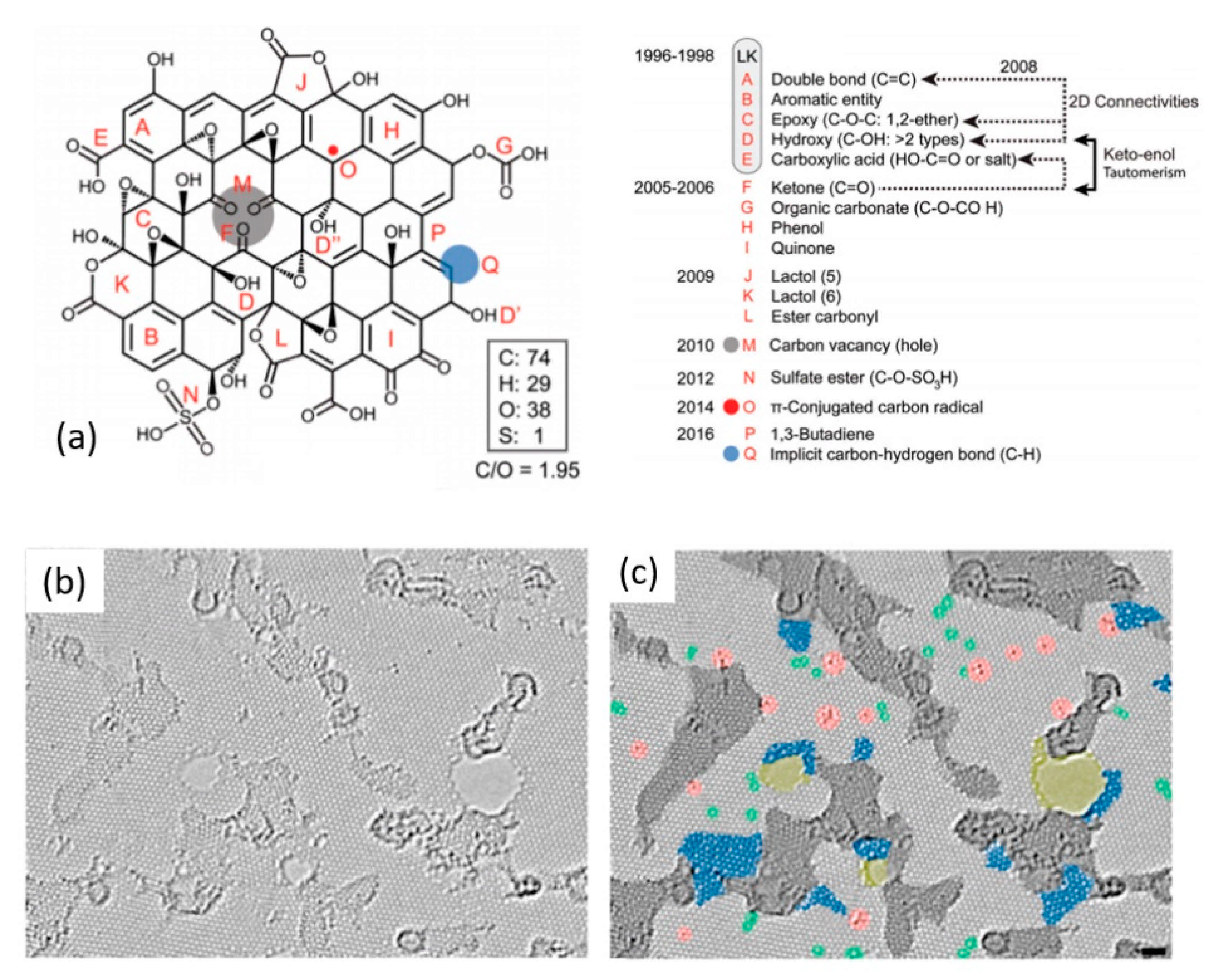
Until today, some ambiguity persists on the precise chemical structure of GO, and several different models describe the same [52,71,72]. The most widely accepted model is the one proposed in 1996 by Lerf and Klinowski (LK) [73,74], originally describing graphite oxide. In the past two decades, various researchers have claimed additional structural changes [75,76]. In a recent review, Brisebois et al. [76] presented a representative structure of GO based on historic and modern models including recently suggested adjustments in the literature (Figure 2a). As shown in Figure 2a, features A–E account for the LK model. The monolayer surface gets its nearly flat carbon-grid from double bonds (A), aromatic entities (B), and epoxide groups (C). Hydroxyl group-containing carbon results in wrinkling of the monolayer. A large number of oxygen-containing groups (C, D, D’, and D”) lie above and below the carbon-grid. Hydroxyl groups (D’) and carboxylic groups (E) terminate the structure of GO. Features such as F, G, H, and I are aspects of the Dékány model [76]. According to Brisebois et al. [76], the complete chemistry of GO is not yet fully understood, and the general LK model should be updated with recently made observations such as carbon vacancies (M), sulfate esters (N), carbon radicals (O), 1,3 butadiene systems (P), and C–H bonds (Q).
The mainly present oxygen-functional groups in GO are epoxides (C-O-C), hydroxyls (-OH), carboxylic (-COOH), and ketone (C=O) ones [77]. The presence of polar groups makes GO hydrophilic and facilitates its exfoliation in aqueous media [78]. The incorporated functional groups cause an increased interlayer distance of >0.625 nm in GO from 0.335 nm in graphite [79,80]. GO has a heterogeneous chemical and electronic structure, and the presence of oxygen-containing groups make it an insulator [35,81]. The sp2 network of carbon atoms, and thus the electrical conductivity, can be substantially restored by various reduction strategies. Figure 2b presents high-resolution imaging of rGO monolayer reduced with H2-plasma [82]. A large portion of crystallized graphene regions with hexagonal lattice (light gray) is observed. The average graphene-like regions here range from 3–6 nm covering 60% of the surface. Carbonaceous adsorbates and trapped contaminants are also observed (dark gray). Other visible features include topological defects (blue and green), individual ad-atoms or substitutions (red), and holes (yellow). Such heterogeneous structure gives rise to properties that are different from pristine graphene. Some of the important properties of GO/rGO are summarized against CVD-graphene in Table 1.
The opportunity for tailoring the optoelectronic properties of GO arises from the ability to manipulate its shape, size, and the fraction of sp2/sp3 hybridized carbon domains by controlled reduction [35,106]. Finally, GO and r-GO serve as a tunable platform for several applications. Table 2 summarizes some of the features and properties of GO/rGO exploited in a wide range of science and technology topics. In optoelectronics, under the field of solar-cells alone, rGO has contributed to the progress of perovskite, perovskite-silicon tandem, dye-sensitized, and organic technologies [107,108,109]. Graphene materials have not been widely utilized for CIGSe as in the case of other solar cell technologies. Nevertheless, CVD–graphene has been incorporated into CIGSe, which includes a demonstration of flexible solar cell [110,111,112]. It is emphasized that GO/rGO can serve as hole-selective contacts and intermediate tunnel junction layer in monolithic CIGSe–Perovskite tandem solar cell applications, which is yet to be reported [113]. Factors such as precursor material-form (powder, dispersion, films, paper, etc.), quality, properties, and application of rGO can influence the choice of reduction method adopted, which is discussed in the following section.
2.2. Reduction Methods for GO
Table 3 lists and summarizes commonly employed reduction methods and some of their important features along with those of the plasma method. Generally, the reduction strategies use either a reductant (chemical, microbial, solvothermal) and/or a thermal, electrical (voltage-induced), radiative (photocatalytic, microwave, plasma), and electrochemical impact [49,119]. Chemical reagents are either used in liquid- or gas-phase for reduction [32,120]. Typically used reagents are fairly hazardous: hydrazine [94], hydrazine hydrate [121], sodium borohydride [122], sodium hydrosulfite [122], and hydrohalic acids [121]. Hydrazine is known to be one of the most powerful reducing agents. However, high toxicity and environmental hazard make it unpopular [123]. By comparing various reducing agents, a study suggested that a reducing agent in combination with acid is beneficial in terms of preserving the rGO surface quality [124]. The processing time in the chemical techniques is relatively longer. In certain cases, the reduction process can consume a day to a week’s time [94,120].
The solvothermal method can yield a stable dispersion of r-GO without the use of additional reductants [131]. However, the C/O atomic ratio and electrical conductivity obtained are inferior to the chemical methods [42,52]. Microbes such as Shewanella [132], E. coli [133], yeast [134], and Azotobacter chroococcum [135] can also reduce GO in the forms of dispersion or film. Though such biological agents are attractive with low-negative environmental impact, they are limited in terms of the need for sensitive culture procedure and prolonged reaction time [49].
High-temperature annealing (up to 1100 °C) aids the removal of oxygenated groups and significantly improves the conductivity of GO-films [136]. This approach is not applicable for temperature-sensitive substrates, like glass or flexible ones. When the preheating and cooling of chambers with active/inert gases or vacuum environment are considered, a substantial amount of energy is consumed, leading to poor energy efficiency. Another significant drawback of the thermal method is the creation of carbon vacancies and other structural defects in the GO plane due to the active diffusion of epoxide groups already at 200 °C [137,138]. Thermogravimetric analysis reveals up to ~70% final mass loss caused by the release of CO and CO2 gases [137]. The photocatalytic reduction of GO heavily relies on the presence of photoactive materials under UV radiation. This makes it suitable only for hybrid nanocomposites [46]. Electrochemical reduction offers a faster, and safer route compared to the previously noticed methods. However, it is not viable for large-scale production, and its degree of reduction is incomparably lower than in the case of the chemical or thermal method [139].
Microwave-assisted reduction of GO can be realized by three routes: (i) chemical reduction, (ii) thermal reduction, and (iii) simultaneous exfoliation and reduction [127]. Microwaves are effectively absorbed by π-electrons that cause very rapid warming of GO (several hundreds of degrees in few seconds) that results in the breaking of weakest bonds [127]. According to this principle, r-GO domains with sp2 carbon network and free π-electrons heat faster than GO-ones that minimize the efficiency of this method [128,129]. When chemically reduced or simultaneously exfoliated and reduced, the quality of r-GO is low and oxygen content is as high as in the case of the conventional thermal method [54,127]. Laser irradiation can also induce local heating in light-absorbing domains of GO and thus be utilized for reduction. The local temperatures can reach 1400 K in this case [140]. In the case of GO films the heat absorbed dissipates to underlying layers and substrate, yielding additional issues. The photothermal reduction (such as the laser and flash techniques) can provide moderate to high atomic C/O ratio (~10 and ~15, respectively) but creates pores, cracks, and voids in GO-films, which could limit its applications [141].
Compared to the previously discussed methods, plasma-assisted reduction techniques are much more attractive for films due to the following reasons. Plasma processes are established and well-controlled, which offers ease of operation also on the industrial scale. Despite relatively expensive equipment, the versatility of plasma processes today forms a vital part of production in various technological fields [67]. Different power generation techniques extended by a wide range of operating pressures including the atmospheric one, as well as the applicability of various active gases, make this approach multidimensional. It opens the way to control the energy of the acting species and tune the chemical footprint of plasma. Moreover, the thermal impact of plasma and the depth of penetrating damage can be also restricted. For attaining graphene-like properties in rGO, significant restoration of the graphitic structure by defect repair is essential. Amongst the available techniques to realize this, the plasma method is one of them, others being the thermally assisted CVD method (>1073 K) and sequential chemical reduction followed by high-temperature graphitization (~2073 K) [48,142]. From environmental, health, and safety aspects, plasma technology has remarkable advantages over chemical and thermal processes [143]. Owing to their advantages, plasmas have demonstrated their attractiveness in the synthesis of graphene and related materials [130,144,145,146].
2.3. Characterization of rGO
The effectiveness of GO reduction is widely assessed based on (i) surface atomic carbon/oxygen ratio (RC/O) and (ii) electrical properties: hole/electron mobility (μ), sheet resistance (RSH), and conductivity (σ). Detailed reports on various GO characterization techniques generally utilized are available in the literature [18,147,148]. When comparing the electrical parameters of various r-GO films, one should consider that monolayers, bi-layers, and tri-layers of r-GO may not differ proportionally. For instance, according to Sinitskii et al. [149], the corresponding conductivities of reduced GO-nanoribbons were found to be 35, 115, and 210 S/cm. In certain cases, such a difference between mono-layers and bi-layers was attributed to the interaction between r-GO and the underlying substrate [150,151]. The RC/O values determined by a surface-sensitive X-ray Photoelectron Spectroscopy (XPS) indicate a degree of reduction. In the case of the layers thicker than 10 nm, XPS is unable to validate the reduction degree in the bulk [152,153].
It is worth noticing characterization of graphene films by Raman spectroscopy, as it provides vital insights. Graphitic materials have Raman features at ~1584 cm−1 (G-band), ~2700 cm−1 (G’-or 2D-band), and ~1350 cm−1 (D-band). The G-band arises from the first-order scattering of E2g phonons of the sp2 carbon atoms in the ring structure, while the D-band appears from the breathing mode of sp2 carbon atoms due to defects [154,155]. The G’-band, unlike the D-band, is not induced by defects and is more prominent in graphene [155]. In graphene, the integrated intensity ratio of G’- and G-band is used to determine the number of layers [22,156]. The G’-band intensity declines, and its full width at half maximum (FWHM) broadens with increasing density of defects [157]. The integrated intensity ratio of D-band and G-band (ID/IG) is widely used for characterizing the defects’ quantity in graphene and related materials. The Tuinstra–Koenig empirical relation [158] based on the ID/IG is used to calculate the in-plane sp2 carbon crystallite size (La). The average distance between point defects (LD) can also be derived from the ID/IG value and the FWHM of the G-band [124,157,159]. Wróblewska et al. [160] highlighted the difficulty in comparison of materials with widely varied ID/IG ratios reported in the literature. For instance, inhomogeneity of GO/r-GO may cause a difference in values measured at distances of a dozen of μm. Additionally, the ratio in question also depends on the laser wavelength used [160]. To reduce uncertainty, a statistical approach (Raman mapping) instead of using single-point measurement should be taken [124,160]. This is unfortunately not the case in every investigation.
Fourier-transform infrared spectroscopy (FTIR) is also a useful tool to investigate the effectiveness of GO-reduction. The presence of various oxygen-containing groups can be recognized in GO/rGO, and thus their removal can be examined [161,162]. The configurations that can be identified with FTIR are [163]:
- epoxide (C-O-C): 1230–1320 cm−1, asymmetric stretching; ~850 cm−1 bending motion,
- sp2-hybridized C=C: 1500–1600 cm−1, in-plane vibrations,
- carboxyl (COOH): 1650–1750 cm−1 (including C-OH vibrations at 3530 and 1080 cm−1),
- ketonic species (C=O): 1600–1650 and 1750–1850cm−1, and
- hydroxyl (namely phenol, C-OH): 3050–3800 and 1070 cm−1) with all C-OH vibrations from COOH and H2O.
3. Plasma-Assisted Reduction of GO
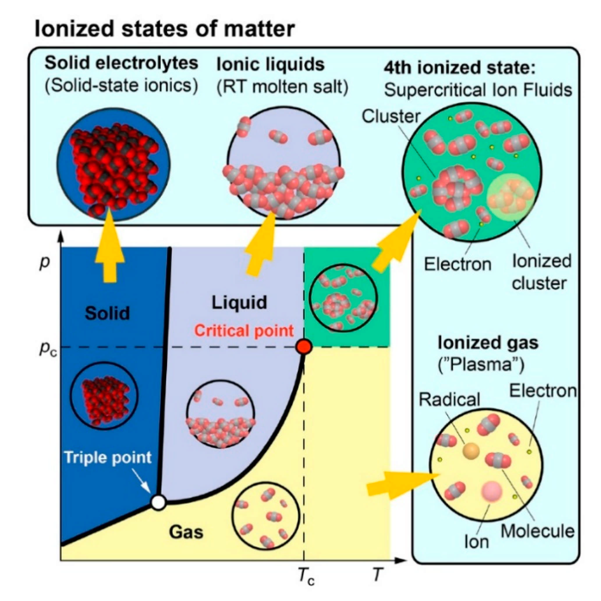
Chemist Irving Langmuir coined the term “plasma” in 1928 [164], which often denotes the fourth state of matter (see Figure 3). In the visible universe, more than 99% of constituents are expected to be in a plasma state (center of active stars, corona flares and sunspots, magnetospheres of the earth, comet-tails, inter-stellar and inter-galactic media, and in the accretion disks around black holes) as opposed to the condensed matter (solids, liquids, and gases) in the form of comets, planets, and cold stars [165,166,167]. Plasma is the ionized form of gases containing energetic ions, free electrons, highly reactive radicals, and photons. The extent of ionization can range from very low values (ionized fraction in the order of 10−4–10−6) up to full ionization [65]. If all species in plasma have the same temperature (or energy), one deals with an equilibrium plasma state. In non-equilibrium plasmas, electrons have higher temperatures than the remaining species. Besides that, laboratory plasma can be divided into high-temperature plasma (or fusion plasma, e.g., in tokamaks, z-pinch system, etc.) and low-temperature plasma (or gas discharge) [65]. The latter is relevant for us, and according to Szabó et al. [168], it can be further classified as follows:
- operating pressure:
- o
- low-pressure plasma
- o
- atmospheric pressure plasma
- temperature:
- o
- low-temperature plasma (Tgas < 2000 K)
- o
- high-temperature plasma (Tgas > 2000 K)
- thermodynamics:
- o
- thermal plasma/equilibrium plasma (Telectron ≈ Tion ≈ Tgas)
- o
- non-thermal plasma/non-equilibrium plasma (Telectron ≫ Tion ≈ Tgas)
- type of coupling:
- o
- inductive coupling
- o
- capacitive coupling
- plasma generation:
- o
- microwave discharge (300 MHz ≤ f ≤ 300 GHz)
- o
- radiofrequency (RF) discharge (ideally 13.56 MHz):
- o
- direct current (DC) discharge
- o
- dielectric barrier discharge (DBD)
- o
- corona discharge
- o
- electric arc
- o
- hollow cathode discharge
- o
- electron beam discharge (EB)
- o
- plasma torch
- o
- alternating current.
Based on the operating pressure, the low-temperature plasmas can be broadly classified into low pressure and atmospheric pressure plasma. Traditional sources of atmospheric plasma include the transferred arcs, plasma torches, corona discharges, dielectric barrier discharges (DBD), and atmospheric-pressure plasma jet (APPJ) [63]. The classical arc torches (ones with local thermal equilibrium) are characterized with high gas temperatures and have been used in applications such as welding, cutting, spraying, etc., where heat is required [169]. Relatively modern low-powered homogeneous arc plasma, generating less heat, is well implanted in the production lines of automobiles, textiles, and packaging, etc. [169]. Corona discharges are spatially non-uniform and are formed on sharp-points, edges, or on thin-wires where the electric field is very large [170]. As the active volume is limited, they are not well suited for the industrial production of large quantities of chemical species [61].
The DBD was developed to overcome disadvantages of the corona discharge [169]. Amongst the atmospheric plasmas, the DBD is better suited for the applications needing volume plasma chemistry, as it caters to large volume excitation with energetic electrons for excitation of atomic and molecular species breaking chemical bonds [61]. The APPJ plasma shares a similar plasma density as the low-pressure plasma but with lower breakdown voltage and electron temperatures than the rest of the plasmas. However, the population of electrons is considered high enough to dissociate many molecules including O2 and N2 [63]. The main disadvantage of the APPJs is the small area that can be treated or coated, which can be circumvented with approaches such as scanning of surface area, using an array of APPJs, and rotating arc root plasma jet process [171]. In a recent review [14], the APPJ-plasma was emphasized to be a promising candidate for large-scale roll-to-roll functionalization of graphene and GO.
The low-pressure plasma emerges from the field of material processing and is a key player in the semiconductor industry [172,173]. Low-pressure plasma treatment of electronic devices, printed circuit boards, and semiconductors are state of the art. Uniform treatment of oxidation-sensitive and three-dimensional objects can be carried out, including cavities that can be processed in large chambers (up to 12,000 L in volume) [174]. They feature some distinctive benefits: (1) uniform glow over large areas, (2) high concentration of reactive species (able to etch or deposit at the rate of up to 10 μm/min), (3) lower breakdown voltages, (4) stable operating window, and (5) sufficient electron temperatures to dissociate molecules with lower gas temperature [63]. On the downside, the vacuum systems are relatively expensive in assembly and maintenance. Furthermore, the processing is limited by batching and transferring materials in and out of the vacuum system. Some of the plasma parameters of low-pressure and atmospheric-pressure plasma are summarized in Table 4.
The plasma-assisted GO-reduction can be regarded analogically to the plasma etching process in a way [66]. It should selectively remove oxygen-containing groups, leaving the carbon network unaffected. On a solid surface exposed to the plasma, two processes track simultaneously: (i) deposition of material and (ii) ablation leading to its removal. Both are determined by the discharge gas and conditions [175]. The ablation of the treated surface can involve sputtering, chemical etching, ion-enhanced energetic etching, and ion-enhanced protective etching [66,175]. In the case of the plasma-assisted chemical etching, the plasma species are excited and become chemically more reactive. In case of the ion-induced etching, plasma activates surface atoms that increase their ability to release under certain pressure and chemical conditions [176,177]. Admixing the inhibitor species into the gas phase results in an isotropic inert coverage of the treated surface, preventing further etching. In sputtering, a bombardment of the surface by the ions with sufficient kinetic energy can break chemical bonds in the solid and eject atoms into a gas phase. Plasma process is quite complex and dynamic where several processes occur simultaneously being subjected to the plasma generation conditions.
The first use of a plasma process for GO reduction was reported in the year 2007 [150], two years following the first report on GO solution processing [31]. Since then, in the last 13 years, several kinds of plasma-assisted reduction processes were developed. To name some ways plasma generation is utilized: radio-frequency (RF) plasma [150,162,178,179,180,181,182,183,184,185,186,187,188,189,190,191,192,193,194,195,196,197], low-pressure direct current (DC) plasma [198,199,200,201], micro-DC plasma [202], atmospheric pressure glow discharge (AGD) plasma [56], electron beam (EB) plasma [203], active screen (AS) plasma [204], atmospheric pressure plasma jet (APPJ) [205] and μ-APPJ [206], and dielectric barrier discharge (DBD) plasma [207,208]. In the following sections, the reduction processes classified according to the discharge gas will be discussed in detail.
3.1. Inert-Gas (He and Ar) Plasma
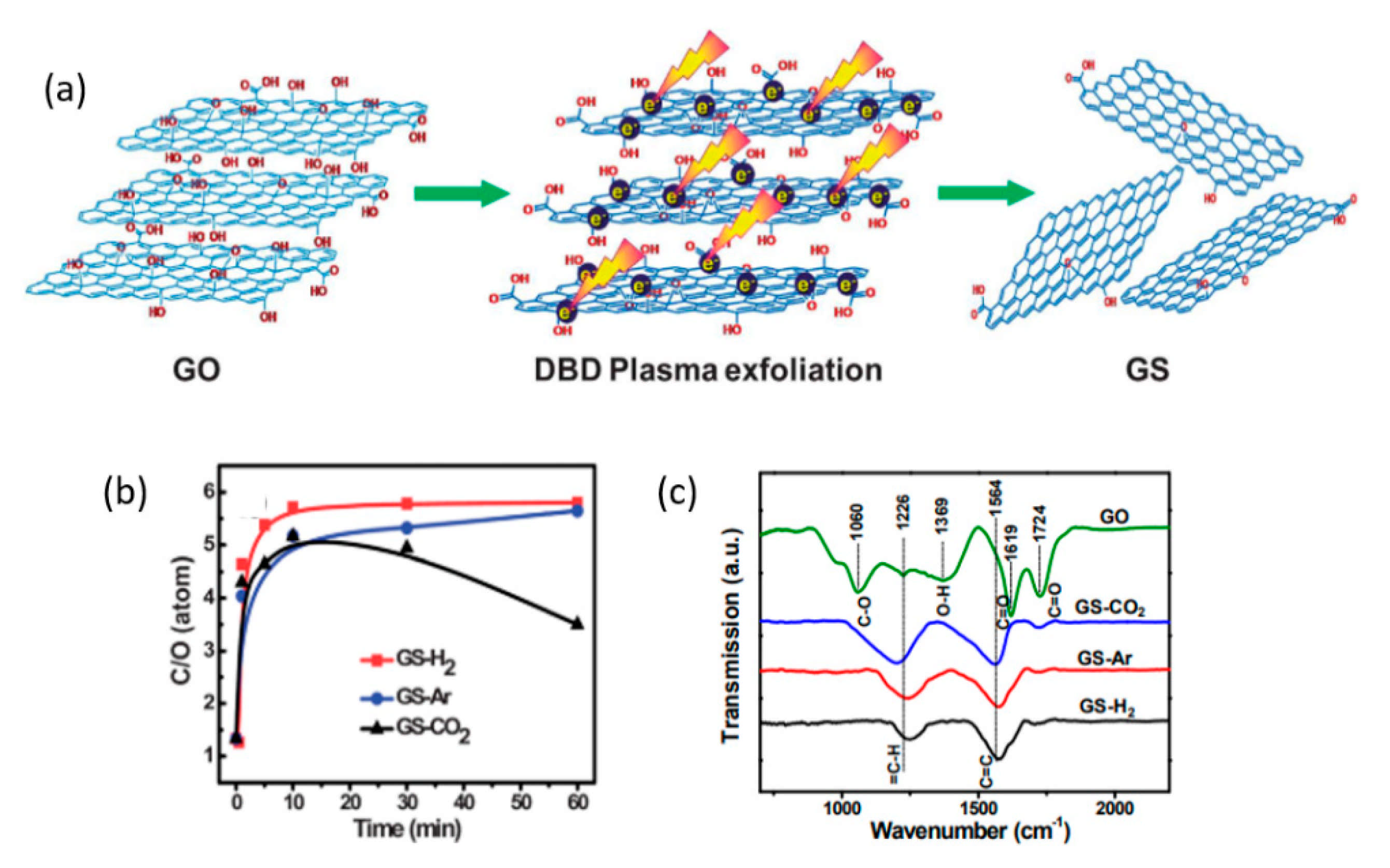
Zhou et al. [209] used a 60 W (AC) DBD plasma with several discharge gases (Ar, H2, and CO2) for simultaneous exfoliation and reduction of GO powder. The plasma treatment mechanism suggested dictates similar for the GO-films. According to this work, the alternating electric field distorts polar bonds in oxygen-containing groups. Furthermore, high-energy electrons and ions of plasma bombard GO surface, rupturing the bonds of oxygen-containing groups within nanoseconds. Jin et al. [210] have shown by first-principle calculations that provision of an electron to the hydroxyl group favors its desorption from the GO surface. The plasmas in general have a high density of electrons (see Table 3); therefore, desorption of hydroxyl groups must be a frequent event. Zhou et al. demonstrated that the deoxygenation of GO was strongly influenced by the discharge gas (see Figure 4). When Ar was employed, deoxygenation occurred primarily through the bombardment of energetic ions and electrons, unlike the H2-plasma, which could also provide chemically reactive plasma species (H, H+, H2+, and H3+ [211]). Other authors have reported that a combination of inert gases and a reactive gas can be more effective in reduction compared to pure inert or reactive gas plasma; this will be discussed in the following sections.
Cardinali et al. [188] used a 25 W RF plasma with Ar for simultaneous thinning and reduction of the bulk GO platelets. Starting from the thickness of ~600 nm, the authors etched samples for 40 min down to 5–6 nm thick multi-layered film with over two orders lower surface electrical resistivity. Although an inert gas plasma does not provide chemically reactive species that can act as reductant, the bombardment by energetic inert ions and electrons have proven to be adequate for deoxygenation in some reports. Bo et al. [200] used an instantaneous 2-s atmospheric-pressure glow discharge process with helium for preparing rGO-paper. The plasma-treated rGO-paper (σ: 59 S/cm; RC/O: 7.6) was on par with the one reduced chemically by hydrazine hydrate (σ: 65 S/cm; RC/O: 8.5). The authors attributed instantaneous deoxygenation with their plasma to the synergy of high-density electrons and heating. The electron density and the neutral gas temperature were determined to be 1.03 × 1016 cm−3 and ~800 K, respectively. Herewith, no damage to the graphitic structure was found by Raman spectroscopy. The r-GO layers reduced by inert-gas plasma have been demonstrated in supercapacitors [200] and H2O2 chemical sensors [162].
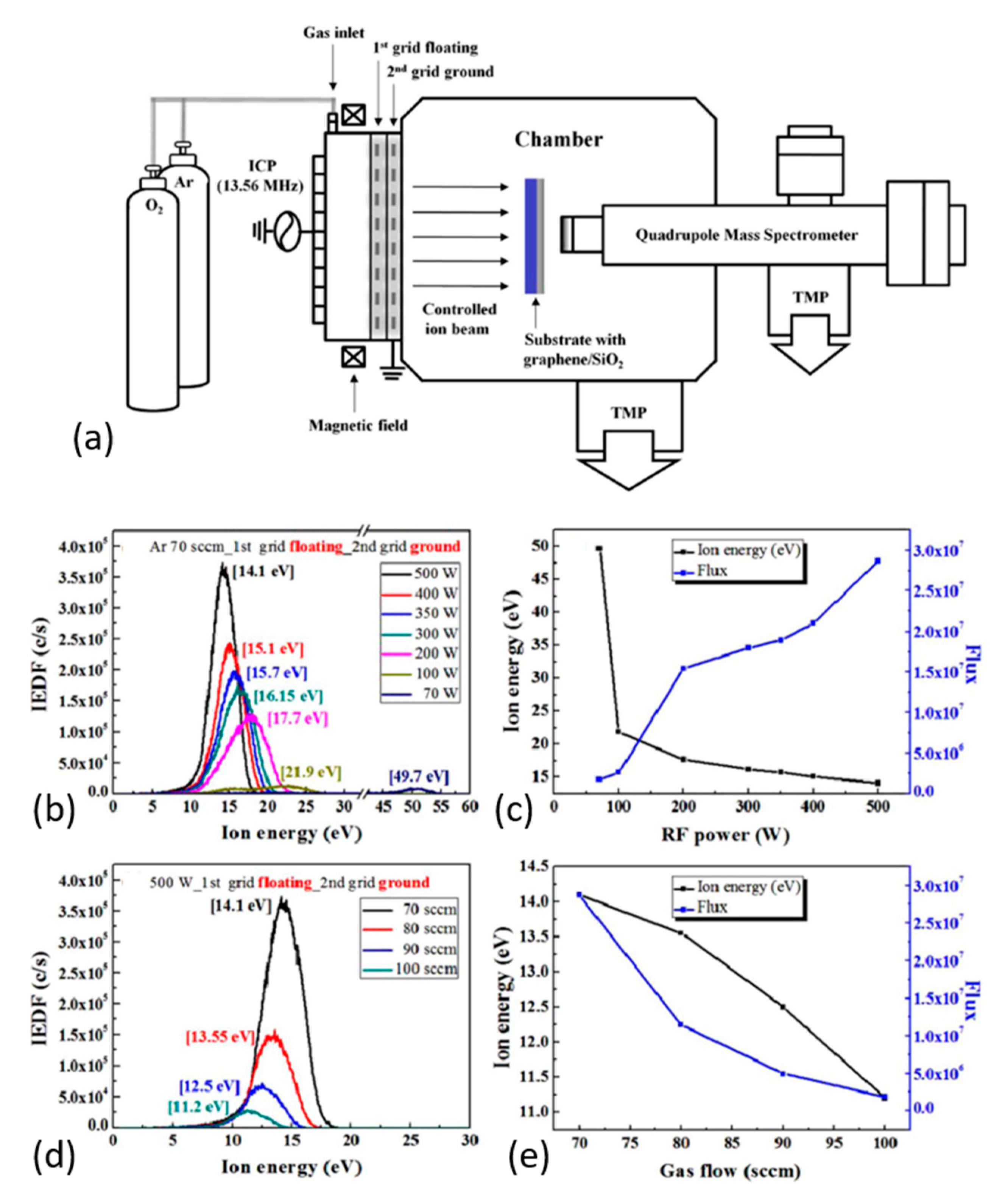
Kim et al. [212] accomplished selectively etching an atomic-layer of graphene without damaging the underneath layers using an inductively-coupled plasma-type ion beam system (see Figure 5a). The cyclic etching process used consisted of chemical adsorption of low-energy oxygen-ions: O2+ and O+ (0–20 eV) followed by physical desorption of oxidized species by Ar+-ions (11.2 eV). To control the energy of ions, the authors applied floated and grounded grids with an axial magnetic field. This approach helped to optimize the process based on ion energy distribution for various power and gas-flows in the system (see Figure 5b–e). This cyclic etch-process exploited the fact that the binding energy of the surface C-atoms decreases from ~6.1 to ~3.9 eV with chemisorption of oxygen ions. At the same time, the C–C binding energy in the underneath layer remains almost unchanged (~0.1 eV). Exactly this fact in combination with controlled energy of Ar+-ions has allowed etching of the top layer selectively. This experience opens the way to combine the chemical and energetic impacts of plasma species for effective and controlled GO reduction.
3.2. Hydrogen Plasma
A hydrogen gas discharge can constitute free electrons, neutrals (molecular H2, atomic H), and charged ions (H+, H−, H2+, H3+) interacting through a set of numerous reactions [213]. A bombardment by H, H+, H2+, and H3+ species with energies varying from 10 eV to few hundred of eV is known to result in the etching of graphene [214,215,216]. The impact of hydrogen plasma on GO is similar to the etching effect and removal of oxygen-containing groups [193,194,208]. A molecular dynamics study [215] on graphene suggested that surface reaction strongly varies with incident atomic H energy: (i) atomic H with few tenths of eV can adsorb on the basal plane of surface-clean graphene, (ii) H energies 0.025–0.3 can selectively etch edges without damaging the basal plane, (iii) H energies in the range 0.3–10 eV hydrogenates basal plane without irreversibly damaging graphene (hydrogenation is reversible), (iv) H energies in the range 10–100 eV are suitable for patterning multi-layer graphene, and (iv) 10 eV H+ ions can etch graphene vertically and the hydrogen plasma containing more molecular (H2+ and H3+) than atomic (H+) ions may induce less subsurface damage in multi-layered graphene. Such detailed studies are yet to be reported for GO materials.
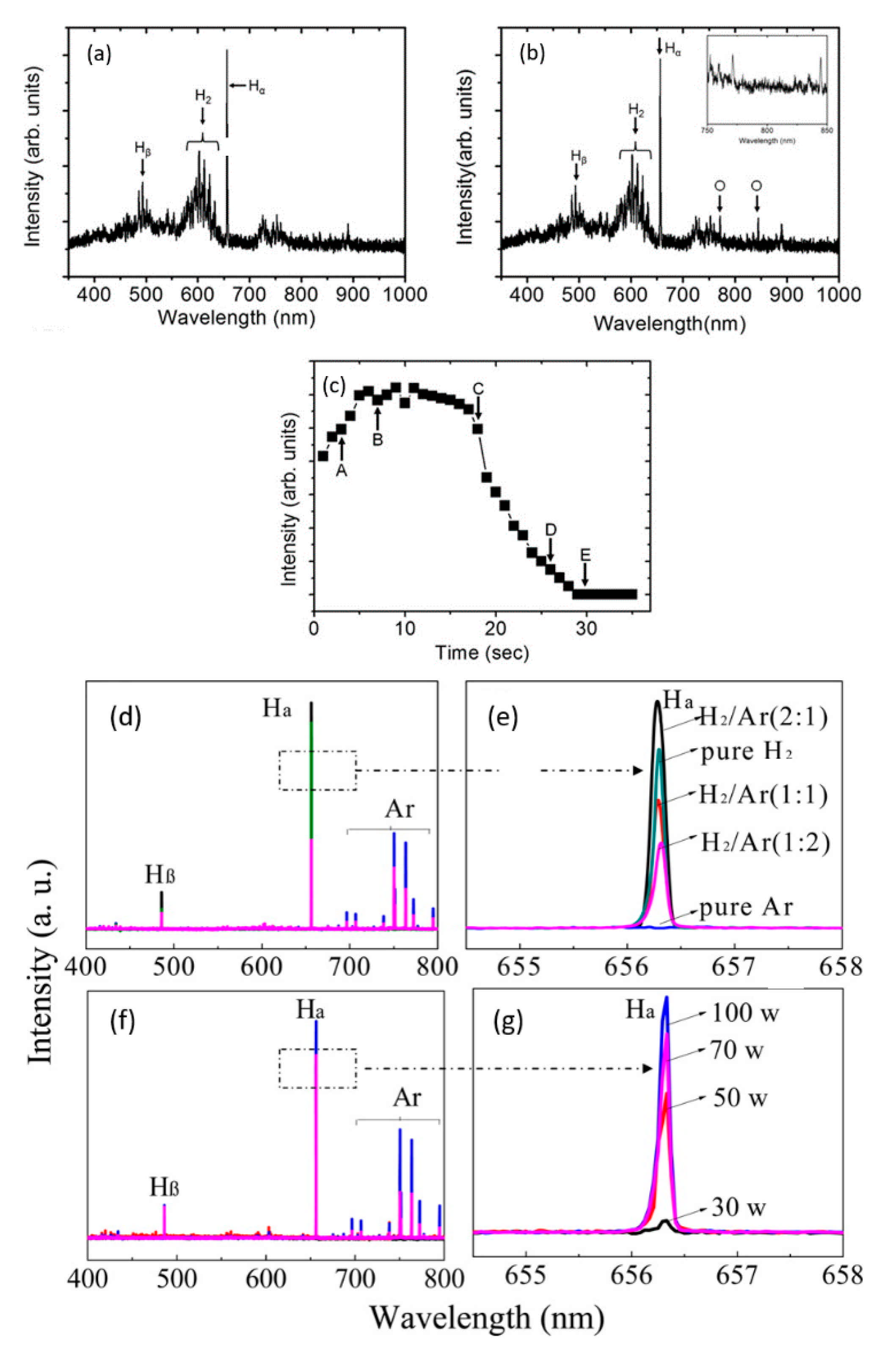
Kim et al. [193] applied optical emission spectroscopy (OES) to determine the optimum process point for GO-reduction to avoid the degradation of electrical characteristics with excess plasma exposure. The emission corresponding to the oxygen radicals released from GO was used as an indicator of the reduction progress (see Figure 6a–c). As observed in Figure 6c, at point C (~18 s after the start of the reduction process), the intensity of the OES oxygen-line begins to decline, indicating the end of reduction. A crucial application of the OES lies in the determination of the excited states of species in the plasma. Li et al. [190] studied with this method the effect of variable plasma power and different gas mixtures (Ar/H2) on the reduction of GO. The emission corresponding to atomic hydrogen (in OES spectra, Figure 6d–g) was found to increase with increasing discharge power and reached an overall maximum for the H2/Ar ratio 2:1. The inclusion of Ar assisted in the enhanced dissociation of H2 due to the penning ionization. The GO (RC/O: 1.1) on reduction with a pure Ar and H2 plasma yielded rGO with RC/O of 1.2 and 1.7, respectively. However, the rGO obtained with a more populous H2/Ar plasma (2:1) resulted in a RC/O up to 6.9. Furthermore, the electrochemical performance of the fabricated rGO was demonstrated as an electrode (in KOH aqueous electrolyte), achieving a specific capacitance of 185.2 F/g. The performance was higher than several graphene-based electrodes in literature.
3.3. Methane Plasma
To obtain graphene-like quality with GO as precursors, numerous investigations into reduction with healing (or repair) of defects has been carried out. By incorporating C-atoms into structural defects of GO, the sp2-hybridized graphene domains are restored. Various strategies employed include thermal-CVD [92,217,218,219] and high-temperature graphitization [142,220]. In a recent review, De Silva et al. [48] addressed the defect repair of GO mostly with thermal methods. This section is devoted to the plasma-enhanced CVD approach, which is more attractive in terms of large-scale applications than the others mentioned.
Methane plasma is a popular choice for the defect repair and reduction of GO. Pure discharge of CH4 [93], as well as in combination with Ar [180,185,203] or H2 [179,184,189,207,221], has been utilized. Cheng et al. [93] treated GO-monolayers on Si/SiO2 substrates with CH4-plasma (100 W, RF, ~575 °C, 10 min) that resulted in a decrease of the ID/IG ratio from 1.03 to 0.53, indicating healing of defects and increasing conversion of sp2 C-atoms. They reported one of the highest conductivities (1590 S/cm) for rGO. Baraket et al. [203] used plasma generated in a CH4 (0–20%)/Ar gas mixture by electron-beam, resulting in the energy of electrons and dissociated ions <0.5 eV and <3 eV, respectively. By varying plasma duty factor, methane concentration, gas pressure, and treatment time, they showed that oxygen concentration in rGO can be controlled in the range 5–43 at.%. Correlating Raman, XPS, and AFM investigations, the authors concluded that the defects originating from deoxygenation were healed by the CHn species. Thus, amorphous carbon was selectively rather than uniformly deposited on rGO. In a mixed gas discharge, the compositional ratio of gases is one of the important parameters to optimize. Yang et al. studied the effect of RF plasma in CH4/Ar mixture (100 W, no substrate heating) on GO-monolayers. They determined that the methane-rich environment (CH4/Ar—2:1) was the most effective for reduction.
Using the CH4 + H2 plasma can be beneficial for the following reasons: (i) the amount of reactive species is surplus for reduction of oxygen-functional groups compared to a pure CH4 plasma [221]; (ii) many defects and distortions of a graphitic network are bound and eliminated by the hydrogen active species and serve at once as active sites for carbon species from plasma to react [179,184], and (iii) the etching nature of H2 plasma restricts deposition of sp3 amorphous carbon from radicals of dissociated CH4 molecules [179,189]. The substrate temperature, CH4/H2 ratio, other plasma conditions, and treatment runtime sensitively influence the relative rates of etching and carbonization (defect restoration). Bodik et al. [207] used an instantaneous DBSCD plasma reduction (100 W/cm3 equimolecular CH4/H2 ratio, atmospheric pressure, 5 s) of the unheated GO films, and observed that this treatment was effective in the removal of oxygen-functional groups but not in sp2-C restoration. Nevertheless, such a plasma process can promote application on temperature-sensitive flexible substrates. Chiang et al. [221] performed a reduction of GO-nanoribbons films with an RF CH4/H2 plasma at 230 °C. Impressively, even at this moderate temperature, the removal of all kinds of oxygen-containing groups (C-O, C=O, and COOH) down to < 1–1.2 at.% surface concentration was determined by XPS analysis. The ID/IG ratio remained however quite high: 0.83.
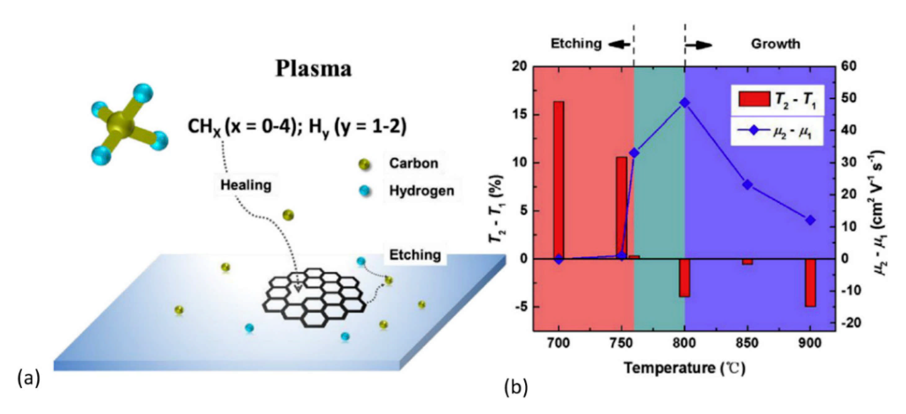
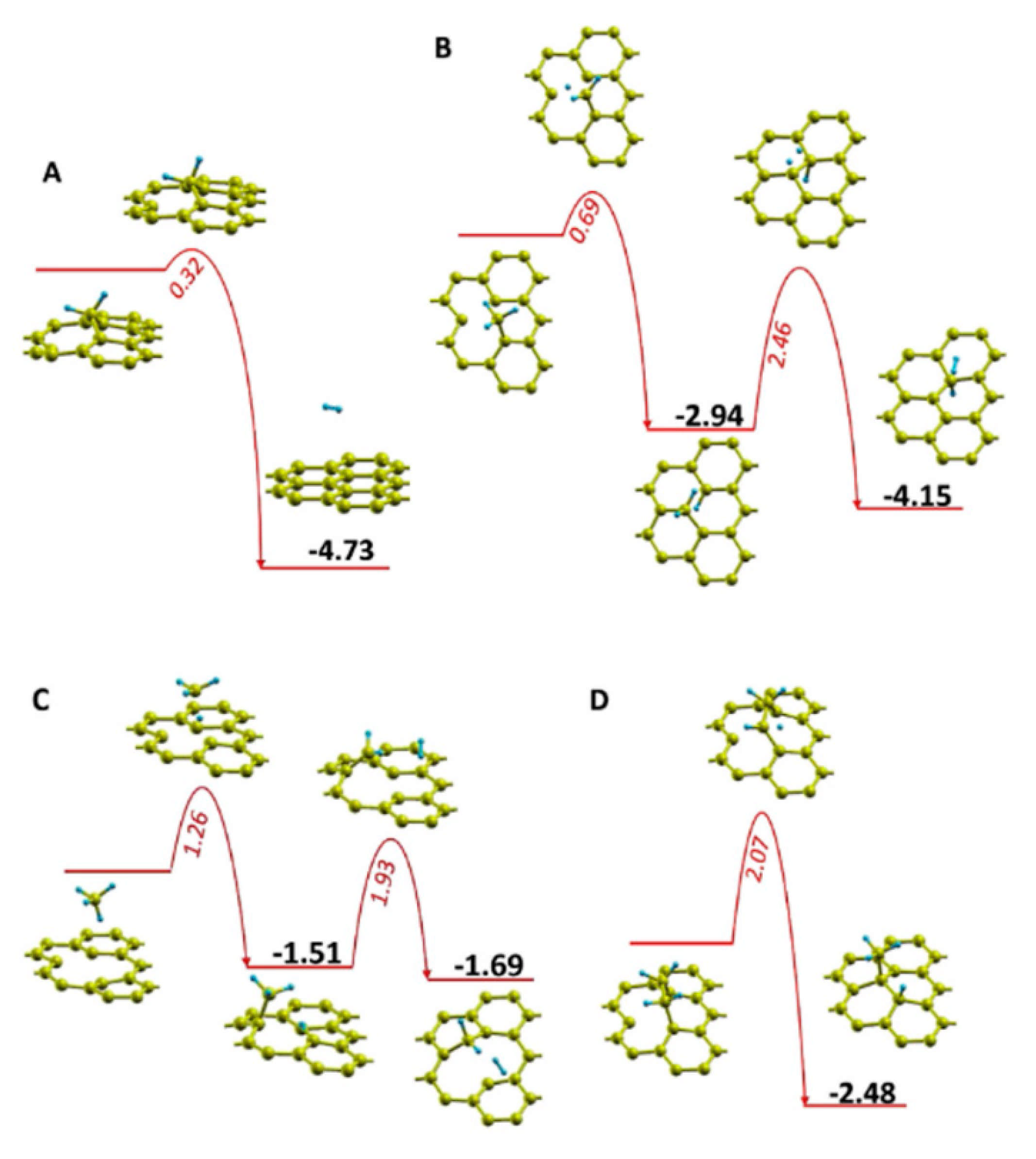
The work of Zhu et al. [179] sheds more light on the influence of temperature in defect healing and its mechanism. Figure 7a presents a schematic where the CHx (x < 4) species (from dissociated CH4) and Hy (y < 2) species (from dissociated H2) are simultaneously involved in the healing and etching process in GO, respectively. As one can see in Figure 7b, the etching by hydrogen plasma interchanges with growing by methane plasma at ~760 °C. After plasma treatment at 800 °C for 40 s, nearly graphene-like films were obtained from GO-sheets. Additionally, Zhu et al. [179] performed density functional theory (DFT) calculations to elucidate different repairing events during thermal annealing in the plasma environment. Migration paths and their associated energy barriers for repairing a carbon mono-vacancy were presented for various derivatives of dissociated CH4 molecule (see Figure 8). As shown in Figure 8, the CH2 species possessed a relatively small energy barrier (0.32 eV) compared to CH3 (0.69 eV), CH4 (1.26 eV), and C2H4 (2.07 eV) species, indicating that the former species dominate in the repair of the carbon mono-vacancies. The authors also suggested that a CH radical could directly fill a mono-vacancy, but a hydrogen atom should simultaneously be taken away by another radical. To our knowledge, there are no other fundamental reports discussing plasma-assisted reduction and repair of GO yet. However, conventional thermal and chemical reduction methods have been relatively well studied and understood [126,210,222,223,224,225].
An interesting question to be understood is whether the reduction and defect healing can be extended to the multi-layered GO, namely, deeper layers that are not directly exposed to plasma. Obata et al. [184,189] demonstrated RF CH4/Ar plasma (10 W, 550 °C) reduced GO-monolayers with electron mobility of 460–900 cm2/V·s and contributed detailed experimental investigations. On the downside, the process needed a remote Cu-film in the vicinity of GO (up to 8 mm distance) to catalyze the reduction and restoration. The authors characterized the plasma effect on mono-, bi-, and tri-layered GO by Raman spectroscopy [184]. As the number of layers increased, the spectra deviated from graphene-like ones and resembled like rGO (larger ID/IG, smaller I2D/IG, wider G-band). This indicated that while the topmost surface changed to restored graphene the deeper layers changed to rGO only. The latter transformation was supposedly driven by the heat of plasma, while the penetration of the dissociated CH4 species was apparently restricted to the top surface layer. Obata et al. [184] attributed this to the selective permeability of graphene and GO, which is in turn dependent on the kinetic diameters of the involved species [226,227]. The defect repair by plasma method thus has a limitation to GO-monolayers [48].
3.4. Nitrogen and Ammonia Plasma
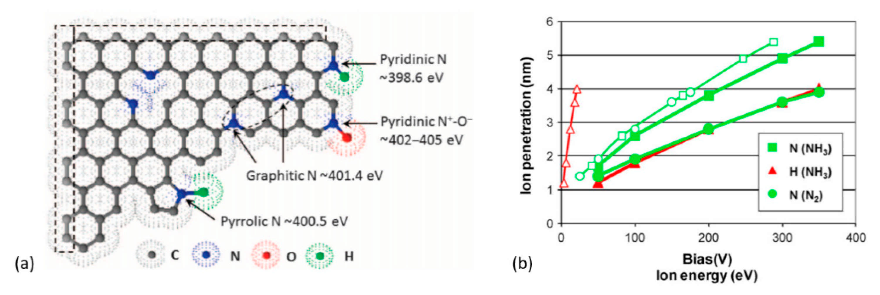
Using the N2 or NH3 plasma treatment is a way to dope graphene by nitrogen [14,228,229]. Amongst various doping techniques available, the plasma-assisted methods yield higher N-atomic concentrations [230]. In the case of GO, plasma treatment not only results in N-doping, but also provokes simultaneous deoxygenation/reduction. The N-atom incorporated into the graphitic network may be pyridine-like, pyrrole-like, or graphite-/quaternary-like (see Figure 9a) [231,232]. The doping of graphene and GO by heteroatoms (boron, nitrogen, phosphorus, sulfur, halogens, etc.) was thoroughly discussed by Wang et al. [233]. Briefly, the quaternary-N defects donate to the graphene lattice ~0.5 free electrons per site [234,235]. In contrast, the pyridinic-N and pyrrolic-N are acceptor defects [235]. However, on hydrogenation, the pyridinic-N doping transforms from p- to n-type [235]. The pyridinic-N and pyrrolic-N sites were suggested to promote electrocatalytic properties [236,237]. N-doped GO materials also have potential for use in fuel-cells [238], water-splitting [239], batteries [240], supercapacitors [241,242], and perovskite solar cells [243].
The dissociation energy of N2 is higher than NH3; therefore, N2 plasma ensures less density of active species than a NH3 plasma for the same given conditions [244]. Additionally, a N2 gas discharge constitutes excited species such as N, N+, N2+, etc. [245], whereas an NH3 plasma can constitute H, N, N2, NH, NH2, N2H2, N2H, NH2+, NH3+, and NH4+ excited species [246,247,248,249]. Well-known reducing agent hydrazine (N2H4) has also been observed at certain conditions in NH3 plasma [250,251]. Thus, more active and reductive NH3 plasma should be more effective than a pure N2 plasma. Charged radicals NxHy (from dissociated NH3, mostly N2H radicals) were suggested to reduce isolated epoxide groups in GO [252], while -NH2 groups were suggested to substitute hydroxyl groups [210]. Mohai et al. [181] subjected GO-films to N2 and NH3 plasma, biasing the sample’s potential to accelerate ions towards the GO-surface. The authors found by XPS that the NH3 plasma effectively reduced the amount of oxygen on the GO surface. The penetration depth of bombarding ions was also computed in this work that revealed the following: (a) biased substrate potential makes penetration depth of N-ions greater than that of H-ions; (b) N-atoms from NH3 could penetrate deeper than those from N2 for a given biasing energy (see Figure 9b).
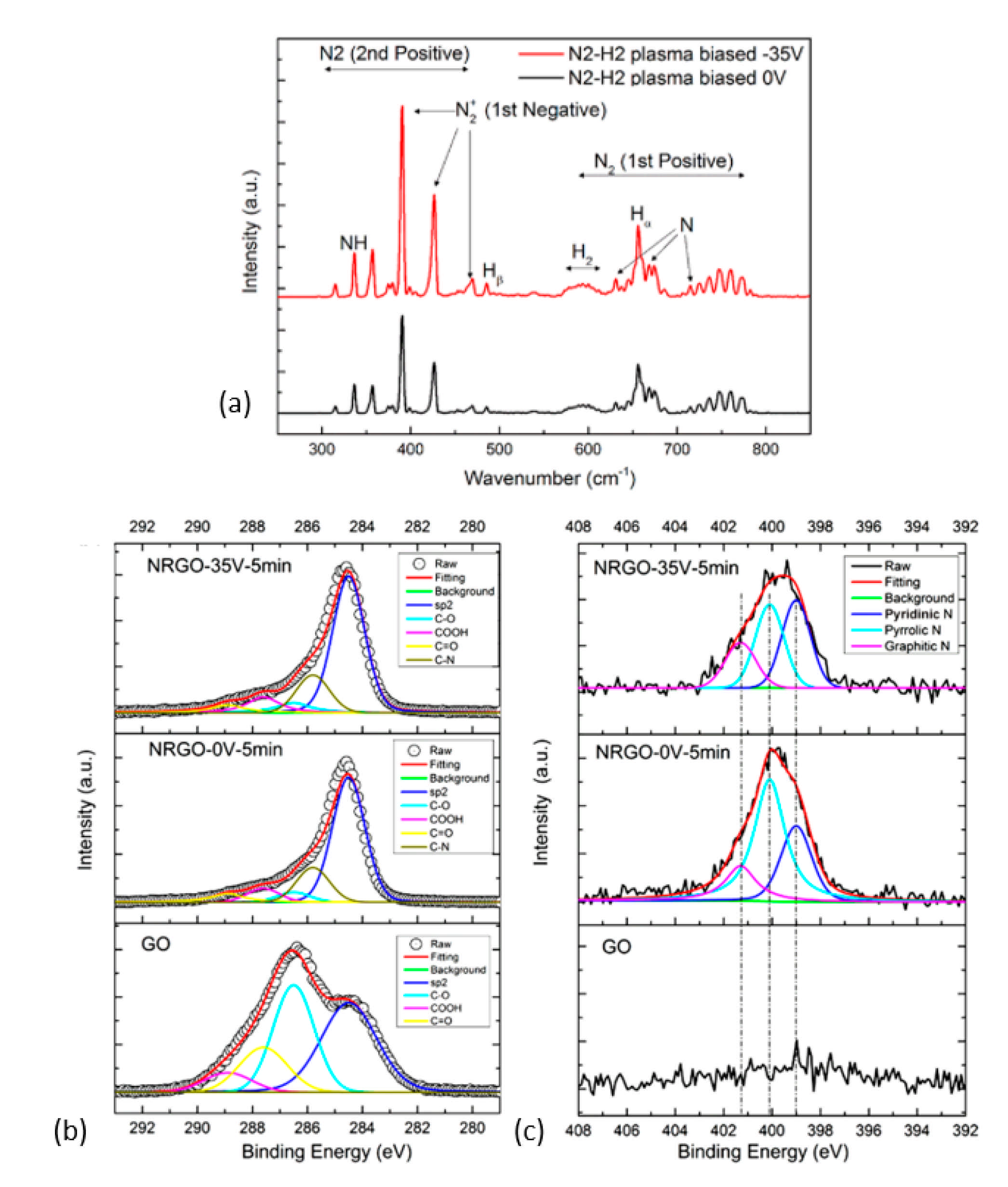
The use of an N2 plasma can be effective when H2 gas is admixed. Zhou et al. [187] used this combination (N2/H2: 40/10 sccm, 1400 W, ICP (~370 kHz)) along with negative-voltage sample biasing (−35 V) to direct and accelerate the positive ions towards the sample surface. The OES data (Figure 10a) confirmed the existence of several radicals from the dissociation of N2 and H2 molecules where the N2+ species dominated. The electron temperature (Te) in plasma increased from 0.55 eV when no bias voltage was used to 0.79 eV in the opposite case. The increase in Te in turn activated more N2 molecules. The •NH radical was attributed to the removal of isolated epoxide groups, while the reactive H-ions was attributed to removal of hydroxyl groups. Using bias voltage also increased the share of graphitic-N sites from 16.88% to 21.11% and pyridinic-N from 27.55% to 38.70% (Figure 10b,c) in the total N-content.
The share of pyridinic, pyrrolic, and graphitic sites in the N-doped rGO varies from report to report based on experimental conditions. A majority of the considered reviews reported that the share of pyrrolic-N was the maximum according to XPS [187,192,195,197,254]. Graphitic-N possessed a high share when processed at higher temperatures [186]. There has been an instance where the graphitic-N share was the highest even after treatment at room temperature [198]. Calculation of formation energies suggested that the substitutional N-doping (graphitic-N) is the most favorable among other configurations [255]. In a presence of carbon vacancy, however, the pyridine-N becomes energetically favorable. Another study pointed out the preference of graphitic-N to appear at carbon atoms near other defects [256]. This study also concluded that pyridine- and pyrrolic-like configurations mostly realized on mono- and di-vacancies. The N-configurations were observed to vary in graphene depending on N2+-ion beam energy and irradiation time [257]. Similarly, sputtering GO with 220 eV N2+-ions for a variable time resulted in different N-configurations and deoxygenation extents [258]. More research must be done in this context for applications where specific N-configuration on GO needs to be tailored.
Lee et al. [197] carried out reduction and nitridation of the 10 nm thick GO-films in the bulk and sheath regions of an NH3 RF plasma (1000 W/m2 power density). The sheath region is characterized by a much stronger electric field than in the glow discharge region that provides domination of ion bombardment [197]. Chemical reactions dominate in-turn in the glowing volume. The XPS investigation revealed that even when placed in a sheath, the GO sample partially lost oxygen and gathered nitrogen, but not as effectively as when treated in a chemically active glow. The samples placed in the sheath were not conductive, which was expected to result from ion bombardment breaking the graphitic network. The authors proposed the following reactions by radicals or ions to be responsible for the reduction of GO in a glowing region of plasma:
where Cg is a carbon atom on the regular graphene site. Equations (1) and (2) explain the reduction of epoxide groups, Equation (3) corresponds to a reduction of the hydroxyl group, and Equations (4) and (5) correspond to that of carboxyl groups on the GO-film.
NH2 + H + Cg-O-Cg → Cg-NH2 + Cg-OH
NH + H2 + Cg-O-Cg → Cg-NH-Cg + H2O
NH2 + H + Cg-OH → Cg-NH2 + H2O
NH2 + H + Cg-COOH → Cg-CO-NH2 + H2O
NH2 + H + Cg-COOH → Cg-NH2 + H2O + CO + H2O
3.5. Acetylene Plasma
An acetylene discharge is also a source of carbon species assisting the healing of GO. To our knowledge, there are only two reports on this topic [186,259]. In both cases, the GO films were annealed in a vacuum (up to 6 h long) before plasma treatment. Such pretreatment could have caused deoxygenation and formation of carbon vacancies, which are active sites for repair. In one of those works, Ooi et al. [259] successfully replaced indium–tin–-oxide (ITO) with C2H2/H2 plasma reduced rGO for an application in a memory device. Before plasma treatment (20 W, 700 °C, 2 min), the GO was thermally annealed at 700 °C for 6 h. Thus, the obtained ~5.12 nm thick rGO film exhibited ~90 cm2/V·s and sheet resistance of ~510 Ω/sq. From the reported thickness and sheet resistance, we estimate the conductivity to be ~3830 S/cm, which is one of the highest reported values for rGO.
Similarly, Haniff et al. [186] prepared rGO on eight-inch Si/SiO2 wafer using C2H2/NH3 plasma (20 W, 700 °C, 3 min) for photodetector application. Before plasma treatment, the films were also annealed in a vacuum (700 °C, 30 min). Since NH3 was added to the discharge gas, the films became N-doped. From the point of the mechanism, it was suggested that active hydrogen species react with oxygen groups at first and eliminate them creating active sites (e.g., point defects and vacancies) for the following N-doping. Simultaneously, the dissociated CxHx (x < 2) and NHx (x < 3) radicals interact with active sites restoring graphitic plane with C- and N-atoms. The photodetectors obtained in this work revealed a photoresponsivity of 0.68 AW−1 at 1.0 V, outperforming graphene-based photoconductor by ~2 orders of magnitude. Although impressive applications have been demonstrated, acetylene (and other carbonaceous gases) has not been studied to the same extent as methane for plasma-assisted defect healing in GO. Theoretical and experimental research is needed to identify which mechanisms and carbonaceous gas discharge are chemically advantageous for low-temperature defect healing. Gong et al. [260] have investigated the defect repair of GO in the presence of water, methanol, and ethanol and concluded that ethanol can contribute better to reduction with increased defect repair in GO.
3.6. Air Plasma
GO-reduction using air as the discharge gas in APPJ-plasma has been demonstrated [205,261]. The APPJ-plasma is created either with a noble gas or air, and the reactive species are generated within the plasma (e.g., He + O2 admixture) or its interaction with the surrounding (air: mostly N2, O2, and H2O vapor) [262]. Thus, various atoms, radicals, ions, and excited molecular species such as: O, O3, 1O2, •OH, N2, N2+, O2•−/•OOH, •NO, ONOO−, OONOO−, H2O2, NO2−, and NO3− are produced [262,263,264] (an example, Figure 11). In an air plasma, active oxygen species stipulate its highly oxidative impact, which is used to remove ad- and chemisorbed organics from the treated surface [265,266,267].
An RF air-plasma (7 W, 49 mL/min, 30 s) has been used to eliminate polymer residues from the surface of transferred CVD-graphene without damaging the graphitic network [268]. Huang et al. [261] treated the surface of the CVD-graphene monolayer with an APPJ-He-plasma (10.7 kV and 14 mA at the electrode, 100 μs short pulses at 1.5 kHz frequency) in ambient air. They observed that as the treatment time progressed from 0–60 s, the concentration of oxygen-containing groups increased from ~10% to ~40%. At longer treatment (>60 s), GO (oxidized CVD-graphene) started losing oxygen together with carbon. The authors suggested that the epoxide groups are unstable under APPJ conditions due to the intensive bombardment by electrons. At C-O-C dissociation, highly reactive radicals like (C-O•) are formed. After activation of epoxide, the transient surface atomic oxygen is captured by surrounding oxygen, forming a di-oxygen molecule as product. The authors suggested that for graphene with high C-O-C coverage, the rate of reduction exceeded that of oxidation.
Alotaibi et al. [205] performed a room-temperature reduction process on GO-films with a scanning atmospheric plasma. Air was used as discharge gas, and a high potential of ~10 kV was applied between the electrodes (300 W, 20 kHz power supply) to generate an arc discharge. The reduced GO realized by the APPJ process was demonstrated in a supercapacitor with a volumetric capacity of 536.55 F/cm3 at a current density of 1 A/g. By combining the plasma jet with software-controlled scanning devices, they were able to demonstrate rapid and controlled GO reduction on several substrates such as glass, plastic, and textile with various shapes and size patterns.
According to the authors, negatively charged oxygen ions participate in bond-breaking, displacement of atoms on the surface, and charge accumulation. Through inelastic collisions, the ions with low kinetic energy bombard the GO-surface, causing rupture of oxygen-containing groups and release of oxygen ions. As a result, the ions O2− and O2− transfer free electrons to the GO-surface and charge it. The formation of nitric oxide (NO) in plasma was also suggested. It can take part in reaction with such groups as -COOH, -CO-, and -OH, converting itself into NO2. On a free-standing 25 μm thick GO film, the reduction process in question produced the exposed to plasma rGO surface with sheet-resistance of 186 Ω/sq in case of 1 min treatment and 160 Ω/sq in case of 2 min treatment. The back rGO side also revealed some reduction extent: Rsh = 680 Ω/sq (1 min) and 560 Ω/sq (2 min), indicating the penetration effect of plasma. To exclude the heating effect of the plasma beam, the authors performed a control experiment by annealing GO in a convection oven for 2–20 min. Fourier transformed infrared spectroscopy analysis revealed that a min of 20-min thermal annealing was required to achieve a comparable reduction degree with a 10 s plasma reduction. Thus, a major impact of plasma by heating was ruled out.
4. Summary and Conclusions
The plasma environment with free-electrons and reactive species reduces GO. In the case of a controlled potential difference between plasma and GO surface, energetic ions bombard the surface, distorting and breaking various chemical bonds. Oxygen-containing groups escape upon further bombardment of plasma species that finally results in GO reduction. Plasma, especially in its equilibrium state, and plasma irradiation generate heat in a treated solid. In that sense, the mechanism of GO reduction by plasma involves dynamic events typical for established thermal reduction. However, plasma processes offer additional parameters to tune: pressure and chemistry of the discharge gas, type and frequency of power generation, and exact treatment time. The set of different types of species (ions, excited atoms or molecules, and electrons) and their relative energy and chemical activity defines the penetration depth and the chemical impact.
Within the scope of reviewed literature here, three main missions of plasma reduction can be distinguished: (I) reduction for improved electrical conductivity (and higher RC/O than initially), which is the general case, (II) reduction with simultaneous doping (mostly by nitrogen), and (III) restoration of graphitic network with mostly sp2-carbon hybridization that means healing of lattice defects. In the general case, all plasma treatments, i.e., based on inert gases (Ar and He) or reactive ones (H2, N2, NH3, CH4, and C2H2) or a combination of them, serve the purpose of reduction. For the second task, plasma needs to contain dopant species (dissociated N2 or NH3) for insertion into the carbon lattice along with reduction. The third task requires the presence of carbon species in plasma for assisting in the healing of GO-defects and increasing sp2-carbon domain size. The corresponding discharge processes are based on a carbonaceous gas (like CH4 and C2H2) and moderate- to high-substrate temperature (230–800 °C). The defect restoration is however limited to monolayers that are nonetheless attractive for the realization of graphene-like electrical properties. Using this approach has already demonstrated conductivities in the order of ~103 (S/cm) and electron mobility ~900 cm2/V.s. To compare, a monolayer film of CVD-graphene has electrical conductivity in the order of 104 S/cm [270,271] and an RC/O of 20 [272]. Certain plasma reduced rGO have attained conductivities in the same magnitude as that of certain highest reported for other techniques such as chemical assisted thermal annealing (acetylene, 1000 °C, 2 h, 1425 S/cm) [273], joule-heating (>2000 K, 1500 S/cm) [274], and two-step treatments: thermal annealing (Ar, 1000 K, 1 h) and joule heating (3000 K, 6300 S/cm), and chemical reduction (hydrazine monohydrate) and graphitization (2700 °C, 5770 S/cm) [220]. These techniques compared to the plasma methods are inferior for large-scale applications. In the case of reduction at a lower temperature regime, which is particularly interesting for flexible applications, the rGO obtained from the plasma method has demonstrated to be superior to those obtained from the thermal method and is comparable to ones obtained from the chemical method [56,162,202].
In certain cases, a mixture of gases can enhance the reduction efficiency of plasma. For instance, in a mixture of inert and reactive gases, active species of the former enhance the dissociation degree of molecules of the reactive gas through penning ionization. Another example: the dissociated hydrogen species (from hydrogen) carry out etching of GO, while the carbon-containing active species (from methane) perform carbon deposition. To optimize such plasma processes, it is crucial to find the right combination of the discharge regime and the ratio of constituent gases for the best cooperative effect. Finally, it is challenging to formulate a single optimal strategy for plasma-assisted reduction of GO just based on the reviewed literature. This arises from the variations (thickness, initial RC/O, the density of defects) of GO-precursors used, different plasma instrumentation and conditions, diversity of measurements, etc. Nevertheless, we collected in this work the factual material, which is crucial for understanding the principles of plasma reduction of graphene oxide.
5. Outlook
As Eigler et al. [124] pointed out, the quality or defectiveness of precursor-GO material influenced by the preparation conditions limits the potential of reduction. The use of large-sized (>10 μm) GO flakes is beneficial over smaller ones due to reduced defect density and improved electrical, thermal, and mechanical properties [54,275]. Additionally, theoretical studies have shown that the proportion between hydroxyl- and epoxide-groups and the total oxygen coverage of initial GO affect the outcome of a reduction process [222,276]. Therefore, improved control of the state-of-the-art GO syntheses and further processing techniques will certainly improve the effectiveness of the subsequent plasma reduction process. Independently, a basic understanding of the reaction mechanisms in plasma and therefore control of its energetic and chemical footprint will allow mastering the GO reduction. This is valid and even more essential for the simultaneous reduction and doping, as well as for the defect healing with sp2-carbon restoration.
A vast majority of the reports are based on low-pressure plasma processes. Breakthroughs with low-temperature and atmospheric-pressure plasma for the same purpose will not just present an opportunity to lower associated costs but importantly facilitate integration with roll-to-roll processing. Low-temperature plasma reduction also will enable novel and niche applications (e.g., in monolithic CIGSe–Perovskite tandem solar cell, as mentioned earlier). Graphene materials are emerging in commercial products, breaking their confinement to academic and research prototypes [277]. Among the graphene-related materials, GO has its significance. According to a 2019 report [278], GO occupies 38% of the market fraction (graphene nanoflakes—52%; CVD-films 10%) with the global production capacity (~784 tons/year in 2017) displaying an increasing trend over the past decade. The global reserve of recoverable graphite exceeds 800 million metric tons as per the 2020 U.S. geological survey [279]. The abundance of raw material reserves along with low-cost and scalable production is encouraging to explore GO/rGO based applications. The amount of scientific research dedicated to plasma technologies has been tremendous over the past decades. However, plasma for GO-reduction has not gained as much substantial attention as the chemical and thermal methods. In today’s material processing world, plasma technology is at the forefront. If backed by persistent research, it is a strong contender for facilitating large-scale applications of rGO.
Author Contributions
Conceptualization and writing—original draft preparation: S.H.B.V.K. and R.M.; writing—review and editing: S.H.B.V.K., R.M. and B.S.; supervision and funding acquisition: B.S. and R.M. All authors have read and agreed to the published version of the manuscript.
Funding
This research was funded by the German Federal Ministry for Economic Affairs and Energy (BMWi) under contract number 0324095H (speedCIGS). The authors acknowledge support by the German Research Foundation and the Open Access Publication Fund of Technische Universität Berlin.
Conflicts of Interest
The authors declare no conflict of interest.
Abbreviations
| 2D | two dimensional |
| σ | conductivity |
| μ-APPJ | micro atmospheric pressure plasma jet |
| A | ampere |
| AC | alternating current |
| AGD | atmospheric-pressure glow discharge plasma |
| APPJ | atmospheric pressure plasma jet |
| AS | active screen |
| CCP | capacitively coupled plasma |
| CIGSe | Cu(In, Ga)(Se, S)2 solar cell |
| CVD | chemical vapor deposition |
| DBD | dielectric barrier discharge |
| DC | direct current |
| FET | field effect transistor |
| GO | graphene oxide |
| hr | hour |
| ICP | inductively coupled plasma |
| kΩ | kilo-Ohm |
| min | minute |
| mTorr | milli-Torr |
| MΩ | mega-Ohm |
| MW | microwave |
| RF | radio frequency |
| rGO | reduced graphene oxide |
| s | second |
| sq | square |
| V | volt |
| V/V | volume/volume |
| W | watt |
Appendix A

Table A1.
Overview of various plasma used for the reduction of GO. Temperature in the “Parameters” column denotes auxiliary heated substrate temperature, when a temperature is not specified no external heating was used. In the “Characteristic changes” column, time indicated in brackets correspond to the reduction duration.
| Serial No. | Year & Reference | Plasma | Characteristic Changes | Application | |||
|---|---|---|---|---|---|---|---|
| Discharge Gas | Generation | Time | Parameters | ||||
| 1 | 2007 [150] | H2 | -- | 5 s | 30 W, 0.8 mbar | σ: 0.05–2 S/cm, ambipolar charge transport | FET |
| 2 | 2010 [203] | 10% CH4 + Ar | Electron beam | 30 s | −2 kV pulse at linear hollow cathode with 150 G Helmholtz coil, 90 mTorr | Controlled reduction with atomic oxygen varied between 43% and 5% | -- |
| 3 | 2011 [188] | Ar | RF | 5–40 min | 25 W, 0.02 mbar, 20 sccm | >2 orders lower surface resistivity. Etching effect with prolonged duration | -- |
| 4 | 2012 [93] | CH4 | RF | 10 min | 100 W, 0.20 Torr, ~575 °C | σ: 1590 S/cm, ID/IG: ~0.53 | -- |
| 5 | 2012 [202] | Ar/H2 (1:1) | DC | 30 min | ~2 kV, 10 mA discharge current, atm. pressure, 150 °C | Sheet resistance 47.7 kΩ/sq (~6 μm), C/O ratio 6.95 | -- |
| 6 | 2013 [192] | NH3 | RF | 3 min | 200W, 500 mTorr, 150 °C, 400 sccm | ~6% N-doped r-GO, σ: 7.4 S/cm, C/O ratio ~9.4 ID/IG: 0.98 (GO:1.09) | -- |
| 7 | 2013 [193] | H2 | RF | <30 s | 200W, 20 mTorr, 150 °C, 300 sccm | σ: 2 S/cm (18 s) and C/O ratio of ~14 (30 s), >18 s exposure causes trade-off between σ & reduction | -- |
| 8 | 2013 [280] | H2 | -- | <10 min | 2 W, 1 Torr | Reduction in sheet resistance by 3~4 orders of magnitude that could be restricted to uppermost layers on short exposure | FET |
| 9 | 2013 [198] | NH3 | DC | 1–20 min | 10–30 W, ~1 Pa | C/O ratio: ~ 6.66, N/C ratio: 15%, work-function change from 4.4 to 3.4 eV, σ: 1–80 S/cm (5 min) | -- |
| 10 | 2013 [191] | (a) NH3 (b) H2 + 10% Ar | - | (a) 4.5–10 min (b) 8.5 min | 160 W, 8 sccm | (a) μe: 5.41 cm2/V.s (8.5 min) and μh: 2.1 cm2/V.s (5.5 min) (b) σ: 630 S/cm for (8.5 min) | FET |
| 11 | 2014 [194] | H2 | RF | 40 s | 10 W, 0.3 mbar, 20 sccm | C/O ratio ~7.9, ID/IG: 0.81 (GO: 0.94), 71% (15%) response at 1500 ppm in N2 (in air) | CO2 gas-sensor |
| 12 | 2014 [199] | H2 | DC | 10 s–5 min | 15 & 30 W, working pressure ~50 Pa, 50–120 °C | σ: 0.2–31 S/cm & μh: 0.1–6 cm2/V.s (15 W, 50 °C, 30 s) | FET |
| 13 | 2014 [195] | NH3 | RF | 30 min | 10 W, 100 mTorr | σ: 1666 S/m, C/O ratio ~4.16 and N/C ratio 9.3%, ID/IG: 1.84 (GO: 2.22) | -- |
| 14 | 2014 [56] | He | AGD | 2 s | −10 kV, discharge current ~1.5–1.9 mA, atmospheric pressure (positive-column plasma) | σ: 5900 S/m, C/O ratio 7.6, surface area: 371 m2/g, specific capacitance 161.6 F/g (1 A/g) | Supercapacitor |
| 15 | 2014 [190] | H2/Ar (various ratio) | RF | 3–10 min | 20–100 W, 4.7 Pa | C/O ratio: 9.6 (100 W, H2/Ar-2:1, 5 min), specific capacitance 185.2 F/g (100 mV/s) for 70 W, H2/Ar-2:1, 5min (C/O ratio 4.2) | Supercapacitor |
| 16 | 2015 [200] | Ar | DC | 4 min | ~10 kV at cathode, 240 mTorr | C/O ratio ~7.9, ID/IG: 0.85, specific capacitance of 190 F/g (10 mV/s) | Supercapacitor |
| 17 | 2015 [196] | H2 | RF | 30 min | 60 W | σ: 3.1 S/cm, μ: 37.5 cm2/V.s | -- |
| 18 | 2015 [204] | 25% N2 + H2 | AS | 60 min | 4 mbar in a traditional 40 kW plasma nitriding unit, 100–200 °C | Doping of N from gas discharge and Fe, Cr, and Mo elements from steel mesh, reduction in resistance from 12.6 MΩ to 50 kΩ (200 °C) | -- |
| 19 | 2015 [197] | NH3 | RF | 1–40 min | 1 kW/m2, 500 mTorr | C/O ratio ~2.7 and N/C ratio ~17% (30 min), σ: 80 S/m (30 min) | -- |
| 20 | 2016 [221] | H2 + CH4 | RF | 5–30 min | 100 W, 240 °C | All oxygen containing groups were removed except ~1.2%, ID/IG: 0.83, RSH: 15 k Ω/sq | -- |
| 21 | 2016 [178] | (a) Ar (b) N2 | RF | 10 min | 100 W, 0.3 Pa, sample biased at 0 V and sample bias from −50 to −300 V | N2-plasma was more effective in reduction (at all sample bias) with relatively higher ion penetration depth | -- |
| 22 | 2017 [207] | H2, CH4, & H2/CH4 (1:1) | DBD | 1–10 s | 1.9 W/cm2, each gas-flow at 0.2 mL/min | ~40% sp2—Carbon restored. Oxidation level in GO reduced from ~50% to ~10% (H2/CH4) | -- |
| 23 | 2017 [179] | 10% CH4 + H2 | RF | ~1 min | Thermal annealing (Ar, 1000 °C, 30 min) followed by plasma treatment: 200 W, 0.34 Torr, 700–900 °C | improvement in μ from 0.01–1 cm2/V.s to 50 cm2/V.s., ID/IG: 0.56 (GO:1.04) | -- |
| 24 | 2017 [259] | 20% H2 + C2H2 | - | 2 min | Thermal annealing (vacuum, 700 °C, 7 hrs.) followed by plasma treatment: 20 W, 50 sccm total flow | μhall: ~90 cm2/V.s, RSH: 510 Ω/sq (5 nm), C/O ratio 10.9, ID/IG: 1.33 (GO:0.97) | Memory device |
| 25 | 2017 [180] | 5% CH4 + Ar | RF | 1–20 min | 700 W/m2, 500 mTorr | transmittance from 91.9% to ~94% at 600 nm & 8.13 MΩ/sq (10 min) | -- |
| 26 | 2018 [181] | (a) NH3 (b) N2 | RF | 10 min | 100 W, 0.3 Pa, sample biased at 0 V and −50 to −350 V | Both plasmas incorporated N into GO, NH3 was more effective in reduction of O-groups | -- |
| 27 | 2018 [208] | H2 | DBD | 1–64 s | 40 W/cm3, atm. pressure | Resistance reduced to 2 MΩ/sq, C/O ratio of ~4.76 (16 s) | -- |
| 28 | 2018 [205] | Air | RF | 10–120 s | 300 W, 20 kHz, ~10 kV (APPJ plasma) | RSH: 186 Ω/sq (25μm), vol. capacitance 536.55 F/cm3 (1 A/g) | Supercapacitor |
| 29 | 2018 [184] | H2/CH4 (1:1) | RF | 10–120 min | 10 W, 9.7–9.8 Pa, H2 & CH4: each at 35 sccm flow, 550–650 °C with Cu catalyst | σ: 930 S/cm, μe: 480 cm2/V.s, ID/IG: ~0.4 | FET |
| 30 | 2018 [183] | H2 | RF | 30 min | 20–60 W | Rise in optical bandgap energy with increase in O-vacancy | -- |
| 31 | 2018 [201] | H2 | DC | 1 min | 15 W, ~0.3 Torr | Threshold of device reduced from 2.6 to 1.8 V, On/Off ratio improved from ~80 to ~103 | Memory device |
| 32 | 2018 [185] | CH4/Ar (1:2 to 2:1) | RF | 1–10 min | 100 W, 50 mTorr, total gas flow 30 sccm | C/O ratio improved from 2.2 to 10.6 & σ: 264 S/m (5 min) | -- |
| 33 | 2019 [189] | H2/CH4 (35:1 to 1:35) | RF | ~0.16–9 hrs | 10 W, 9.7–9.8 Pa, total flow 350 sccm, 550 °C with Cu catalyst | Moderate restored r-GO in ~15 min for CH4 rich condition, high crystallinity for H2 rich condition: μe: 900 cm2/V.s, ID/IG: 0.17 | -- |
| 34 | 2019 [186] | 20% C2H2 + NH3 | - | 3 min | annealing at 700 °C (30 min, 10−4 mbar); followed by 3 min plasma: 20 W, 2 mbar, 50 sccm total flow | C/O ratio 8.34, μe: 60–80 cm2/V.s, photoresponsivity of 0.68 A/W at 1 V | Photodetector |
| 35 | 2019 [187] | 20% H2 + N2 | RF | 5–80 min | 1400 W at ~370 kHz, 50 sccm total flow, sample with 0 and −35 V bias | DC bias contributed to efficient reduction and recovery of GO (lowest ID/IG ratio). Resistance change between ~425–570 kΩ for 0–1.5% strain | Stress sensor |
| 36 | 2019 [162] | Ar | RF | 30–120 min | 300 W, 650 mTorr | resistance of 2 kΩ/sq (120 min), mean sensor sensitivity of 277 ± 80 µA/mM.cm2; Pt reference 5.2 ± 0.51 µA/mM.cm2 | H2O2 sensor |
| 37 | 2020 [206] | 1% He + N2 & He + H2 | RF | 5 s–3 min | 4 W, flow: 2000 sccm N2 & 16 sccm He (µAPPJ plasma) | Sheet resistance: ~4 MΩ/sq (He + N2), ~0.24 MΩ/sq (He + H2); GO ~138 MΩ/sq | -- |
References
- Boehm, H.P.; Setton, R.; Stumpp, E. Nomenclature and terminology of graphite intercalation compounds. Synth. Metals 1985, 11, 363–371. [Google Scholar] [CrossRef]
- Larousserie, D. Graphene—The New Wonder Material. Available online: https://www.theguardian.com/science/2013/nov/26/graphene-molecule-potential-wonder-material (accessed on 8 June 2020).
- Wallace, P.R. The Band Theory of Graphite. Phys. Rev. 1947, 71, 622. [Google Scholar] [CrossRef]
- McClure, J.W. Diamagnetism of Graphite. Phys. Rev. 1956, 104, 666–671. [Google Scholar] [CrossRef]
- Slonczewski, J.C.; Weiss, P.R. Band Structure of Graphite. Phys. Rev. 1958, 109, 272–279. [Google Scholar] [CrossRef]
- Semenoff, G.W. Condensed-Matter Simulation of a Three-Dimensional Anomaly. Phys. Rev. Lett. 1984, 53, 2449–2452. [Google Scholar] [CrossRef]
- Fradkin, E. Critical behavior of disordered degenerate semiconductors. II. Spectrum and transport properties in mean-field theory. Phys. Rev. B 1986, 33, 3263–3268. [Google Scholar] [CrossRef]
- Haldane, F.D.M. Model for a Quantum Hall Effect without Landau Levels: Condensed-Matter Realization of the “Parity Anomaly”. Phys. Rev. Lett. 1988, 61, 2015–2018. [Google Scholar] [CrossRef]
- Geim, A.K.; Novoselov, K.S. The rise of graphene. Nat. Mater. 2007, 6, 183–191. [Google Scholar] [CrossRef]
- Warner, J.H.; Schäffel, F.; Bachmatiuk, A.; Rümmeli, M.H. Properties of Graphene. In Graphene; Elsevier: Amsterdam, The Netherlands, 2013; pp. 61–127. [Google Scholar]
- Novoselov, K.S.; Fal, V.I.; Colombo, L.; Gellert, P.R.; Schwab, M.G.; Kim, K. A roadmap for graphene. Nature 2012, 490, 192–200. [Google Scholar] [CrossRef]
- Scott Bunch, J.; Verbridge, S.S.; Alden, J.S.; van der Zande, A.M.; Parpia, J.M.; Craighead, H.G.; McEuen, P.L. Impermeable Atomic Membranes from Graphene Sheets. Nano Lett. 2008, 8, 2458–2462. [Google Scholar] [CrossRef] [Green Version]
- Garg, R.; Dutta, N.; Choudhury, N. Work Function Engineering of Graphene. Nanomaterials 2014, 4, 267–300. [Google Scholar] [CrossRef] [PubMed] [Green Version]
- Dey, A.; Chroneos, A.; Braithwaite, N.S.J.; Gandhiraman, R.P.; Krishnamurthy, S. Plasma engineering of graphene. Appl. Phys. Rev. 2016, 3, 021301. [Google Scholar] [CrossRef] [Green Version]
- Bonaccorso, F.; Lombardo, A.; Hasan, T.; Sun, Z.; Colombo, L.; Ferrari, A.C. Production and processing of graphene and 2d crystals. Mater. Today 2012, 15, 564–589. [Google Scholar] [CrossRef]
- Raccichini, R.; Varzi, A.; Passerini, S.; Scrosati, B. The role of graphene for electrochemical energy storage. Nat. Mater. 2015, 14, 271–279. [Google Scholar] [CrossRef] [PubMed]
- Zhu, Y.; Ji, H.; Cheng, H.M.; Ruoff, R.S. Mass production and industrial applications of graphene materials. Natl. Sci. Rev. 2018, 5, 90–101. [Google Scholar] [CrossRef] [Green Version]
- Backes, C.; Abdelkader, A.M.; Alonso, C.; Andrieux-Ledier, A.; Arenal, R.; Azpeitia, J.; Balakrishnan, N.; Banszerus, L.; Barjon, J.; Bartali, R.; et al. Production and processing of graphene and related materials. 2D Mater. 2020, 7, 022001. [Google Scholar] [CrossRef]
- Novoselov, K.S.; Geim, A.K.; Morozov, S.V.; Jiang, D.; Zhang, Y.; Dubonos, S.V.; Grigorieva, I.V.; Firsov, A.A. Electric Field Effect in Atomically Thin Carbon Films. Science 2004, 306, 666–670. [Google Scholar] [CrossRef] [Green Version]
- Warner, J.H.; Schäffel, F.; Bachmatiuk, A.; Rümmeli, M.H.; Ibrahim, I. Chapter 4: Methods for Obtaining Graphene. In Graphene: Fundamentals and Emergent Applications; Elsevier: Waltham, MA, USA, 2013; pp. 129–228. [Google Scholar]
- Lin, Y.M.; Dimitrakopoulos, C.; Jenkins, K.A.; Farmer, D.B.; Chiu, H.Y.; Grill, A.; Avouris, P. 100-GHz Transistors from Wafer-Scale Epitaxial Graphene. Science 2010, 327, 662. [Google Scholar] [CrossRef] [Green Version]
- Li, X.; Cai, W.; An, J.; Kim, S.; Nah, J.; Yang, D.; Piner, R.; Velamakanni, A.; Jung, I.; Tutuc, E.; et al. Large-Area Synthesis of High-Quality and Uniform Graphene Films on Copper Foils. Science 2009, 324, 1312–1314. [Google Scholar] [CrossRef] [Green Version]
- Mattevi, C.; Kim, H.; Chhowalla, M. A review of chemical vapour deposition of graphene on copper. J. Mater. Chem. 2011, 21, 3324–3334. [Google Scholar] [CrossRef]
- Hernandez, Y.; Nicolosi, V.; Lotya, M.; Blighe, F.M.; Sun, Z.; De, S.; McGovern, I.T.; Holland, B.; Byrne, M.; Gun’Ko, Y.K.; et al. High-yield production of graphene by liquid-phase exfoliation of graphite. Nat. Nanotechnol. 2008, 3, 563–568. [Google Scholar] [CrossRef] [PubMed] [Green Version]
- Wei, D.; Grande, L.; Chundi, V.; White, R.; Bower, C.; Andrew, P.; Ryhänen, T. Graphene from electrochemical exfoliation and its direct applications in enhanced energy storage devices. Chem. Commun. 2012, 48, 1239–1241. [Google Scholar] [CrossRef] [PubMed]
- Paton, K.R.; Varrla, E.; Backes, C.; Smith, R.J.; Khan, U.; O’Neill, A.; Boland, C.; Lotya, M.; Istrate, O.M.; King, P.; et al. Scalable production of large quantities of defect-free few-layer graphene by shear exfoliation in liquids. Nat. Mater. 2014, 13, 624–630. [Google Scholar] [CrossRef] [PubMed]
- Karagiannidis, P.G.; Hodge, S.A.; Lombardi, L.; Tomarchio, F.; Decorde, N.; Milana, S.; Goykhman, I.; Su, Y.; Mesite, S.V.; Johnstone, D.N.; et al. Microfluidization of Graphite and Formulation of Graphene-Based Conductive Inks. ACS Nano 2017, 11, 2742–2755. [Google Scholar] [CrossRef] [Green Version]
- Cui, X.; Zhang, C.; Hao, R.; Hou, Y. Liquid-phase exfoliation, functionalization and applications of graphene. Nanoscale 2011, 3, 2118–2126. [Google Scholar] [CrossRef]
- Yang, X.; Yu, X.; Liu, X. Obtaining a sustainable competitive advantage from patent information: A patent analysis of the graphene industry. Sustainability 2018, 10, 4800. [Google Scholar] [CrossRef] [Green Version]
- Chen, K.; Shi, L.; Zhang, Y.; Liu, Z. Scalable chemical-vapour-deposition growth of three-dimensional graphene materials towards energy-related applications. Chem. Soc. Rev. 2018, 47, 3018–3036. [Google Scholar] [CrossRef]
- Stankovich, S.; Piner, R.D.; Chen, X.; Wu, N.; Nguyen, T.; Ruoff, R.S. Stable aqueous dispersions of graphitic nanoplatelets via the reduction of exfoliated graphite oxide in the presence of poly (sodium 4-styrenesulfonate). J. Mater. Chem. 2006, 16, 155–158. [Google Scholar] [CrossRef]
- Stankovich, S.; Dikin, D.A.; Piner, R.D.; Kohlhaas, K.A.; Kleinhammes, A.; Jia, Y.; Wu, Y. Synthesis of graphene-based nanosheets via chemical reduction of exfoliated graphite oxide. Carbon 2007, 45, 1558–1565. [Google Scholar] [CrossRef]
- Yu, X.; Cheng, H.; Zhang, M.; Zhao, Y.; Qu, L.; Shi, G. Graphene-based smart materials. Nat. Rev. Mater. 2017, 2, 1–14. [Google Scholar] [CrossRef]
- Eftekhari, A.; Garcia, H. The necessity of structural irregularities for the chemical applications of graphene. Mater. Today Chem. 2017, 4, 1–16. [Google Scholar] [CrossRef]
- Loh, K.P.; Bao, Q.; Eda, G.; Chhowalla, M. Graphene oxide as a chemically tunable platform for optical applications. Nat. Chem. 2010, 2, 1015–1024. [Google Scholar] [CrossRef] [PubMed]
- Eda, G.; Chhowalla, M. Chemically derived graphene oxide: Towards large-area thin-film electronics and optoelectronics. Adv. Mater. 2010, 22, 2392–2415. [Google Scholar] [CrossRef] [PubMed]
- Yang, Y.; Han, C.; Jiang, B.; Iocozzia, J.; He, C.; Shi, D.; Jiang, T.; Lin, Z. Graphene-based materials with tailored nanostructures for energy conversion and storage. Mater. Sci. Eng. R Rep. 2016, 102, 1–72. [Google Scholar] [CrossRef]
- El-Kady, M.F.; Shao, Y.; Kaner, R.B. Graphene for batteries, supercapacitors and beyond. Nat. Rev. Mater. 2016, 1, 1–14. [Google Scholar] [CrossRef]
- Bahamonde, J.P.; Nguyen, H.N.; Fanourakis, S.K.; Rodrigues, D.F. Recent advances in graphene—Based biosensor technology with applications in life sciences. J. Nanobiotechnol. 2018, 16, 1–17. [Google Scholar] [CrossRef] [Green Version]
- Yadav, R.; Subhash, A.; Chemmenchery, N.; Kandasubramanian, B. Graphene and Graphene Oxide for Fuel Cell Technology. Ind. Eng. Chem. Res. 2018, 57, 9333–9350. [Google Scholar] [CrossRef]
- Yan, M.; Xiang, T.; Yu, X.; Xiao, J.; Li, W.; Ku, Z.; Huang, F.; Zhong, J.; Peng, Y.; Cheng, Y.-B. Room-temperature Sputtered NiOx for hysteresis-free and stable inverted Cs-FA mixed-cation perovskite solar cells. Mater. Sci. Semicond. Process. 2020, 115, 105129. [Google Scholar] [CrossRef]
- Thakur, S.; Karak, N. Alternative methods and nature-based reagents for the reduction of graphene oxide—A review. Carbon 2015, 94, 224–242. [Google Scholar] [CrossRef]
- Zhang, P.; Li, Z.; Zhang, S.; Shao, G. Recent Advances in Effective Reduction of Graphene Oxide for Highly Improved Performance Toward Electrochemical Energy Storage. Energy Environ. Mater. 2018, 1, 5–12. [Google Scholar] [CrossRef] [Green Version]
- Aunkor, M.T.H.; Mahbubul, I.M.; Saidur, R.; Metselaar, H.S.C. The green reduction of graphene oxide. RSC Adv. 2016, 6, 27807–27828. [Google Scholar] [CrossRef]
- De Silva, K.K.H.; Huang, H.-H.; Joshi, R.K.; Yoshimura, M. Chemical reduction of graphene oxide using green reductants. Carbon 2017, 119, 190–199. [Google Scholar] [CrossRef]
- Taniselass, S.; Md Arshad, M.K.; Gopinath, S.C.B. Current state of green reduction strategies: Solution-processed reduced graphene oxide for healthcare biodetection. Mater. Sci. Eng. C 2019, 96, 904–914. [Google Scholar] [CrossRef] [PubMed]
- Ismail, Z. Green reduction of graphene oxide by plant extracts: A short review. Ceram. Int. 2019, 45, 23857–23868. [Google Scholar] [CrossRef]
- De Silva, K.K.H.; Huang, H.-H.; Joshi, R.; Yoshimura, M. Restoration of the graphitic structure by defect repair during the thermal reduction of graphene oxide. Carbon 2020, 166, 74–90. [Google Scholar] [CrossRef]
- Feng, J.; Ye, Y.; Xiao, M.; Wu, G.; Ke, Y. Synthetic routes of the reduced graphene oxide. Chem. Pap. 2020, 74, 3767–3783. [Google Scholar] [CrossRef]
- Jakhar, R.; Yap, J.E.; Joshi, R. Microwave reduction of graphene oxide. Carbon 2020, 170, 277–293. [Google Scholar] [CrossRef]
- Agarwal, V.; Zetterlund, P.B. Strategies for reduction of graphene oxide—A comprehensive review. Chem. Eng. J. 2021, 405, 127018. [Google Scholar] [CrossRef]
- Pei, S.; Cheng, H. The reduction of graphene oxide. Carbon 2012, 50, 3210–3228. [Google Scholar] [CrossRef]
- Mao, S.; Pu, H.; Chen, J. Graphene oxide and its reduction: Modeling and experimental progress. RSC Adv. 2012, 2, 2643–2662. [Google Scholar] [CrossRef]
- Dong, L.; Yang, J.; Chhowalla, M.; Loh, K.P. Synthesis and reduction of large sized graphene oxide sheets. Chem. Soc. Rev. 2017, 46, 7306–7316. [Google Scholar] [CrossRef] [PubMed]
- Neustroev, E.P. Plasma Treatment of Graphene Oxide. In Graphene Oxide—Applications and Opportunities; Kamble, G., Ed.; IntechOpen: London, UK, 2018; pp. 7–24. [Google Scholar]
- Bo, Z.; Zhu, W.; Tu, X.; Yang, Y.; Mao, S.; He, Y.; Chen, J.; Yan, J.; Cen, K. Instantaneous Reduction of Graphene Oxide Paper for Supercapacitor Electrodes with Unimpeded Liquid Permeation. J. Phys. Chem. C 2014, 118, 13493–13502. [Google Scholar] [CrossRef]
- Nair, R.R.; Wu, H.A.; Jayaram, P.N.; Grigorieva, I.V.; Geim, A.K. Unimpeded Permeation of Water through Helium-Leak-Tight Graphene-Based Membranes. Science 2012, 335, 442–444. [Google Scholar] [CrossRef] [Green Version]
- Ma, Y.; Fang, S.; Wang, Q. The tunable plasma synthesis of Pt-reduced graphene oxide nanocomposites. AIP Adv. 2017, 7, 065118. [Google Scholar] [CrossRef]
- Ke, Z.; Ma, Y.; Zhu, Z.; Zhao, H.; Wang, Q.; Huang, Q. Non-thermal hydrogen plasma processing effectively increases the antibacterial activity of graphene oxide. Appl. Phys. Lett. 2018, 112, 013701. [Google Scholar] [CrossRef]
- Abdelkader-Fernández, V.K.; Melguizo, M.; Domingo-García, M.; López-Garzón, F.J.; Pérez-Mendoza, M. Hydrogen cold plasma for the effective reduction of graphene oxide. Appl. Surf. Sci. 2019, 464, 673–681. [Google Scholar] [CrossRef]
- Eliasson, B.; Kogelschatz, U. Nonequilibrium Volume Plasma Chemical Processing. IEEE Trans. Plasma Sci. 1991, 19, 1063–1077. [Google Scholar] [CrossRef]
- Hopwood, J. Review of inductively coupled plasmas for plasma processing. Plasma Sources Sci. Technol. 1992, 1, 109–116. [Google Scholar] [CrossRef]
- Schütze, A.; Jeong, J.Y.; Babayan, S.E.; Park, J.; Selwyn, G.S.; Hicks, R.F. The atmospheric-pressure plasma jet: A review and comparison to other plasma sources. IEEE Trans. Plasma Sci. 1998, 26, 1685–1694. [Google Scholar] [CrossRef] [Green Version]
- Conrads, H.; Schmidt, M. Plasma generation and plasma sources. Plasma Sour. Sci. Technol. 2000, 9, 441–454. [Google Scholar] [CrossRef] [Green Version]
- Bogaerts, A.; Neyts, E.; Gijbels, R.; Van der Mullen, J. Gas discharge plasmas and their applications. Spectrochim. Acta Part B At. Spectrosc. 2002, 57, 609–658. [Google Scholar] [CrossRef]
- Lieberman, M.A.; Lichtenberg, A.J. Principles of Plasma Discharges and Materials Processing, 2nd ed.; John Wiley & Sons: Hoboken, NJ, USA, 2005. [Google Scholar]
- Adamovich, I.; Baalrud, S.D.; Bogaerts, A.; Bruggeman, P.J.; Cappelli, M.; Colombo, V.; Czarnetzki, U.; Ebert, U.; Eden, J.G.; Favia, P.; et al. The 2017 Plasma Roadmap: Low temperature plasma science and technology. J. Phys. D Appl. Phys. 2017, 50, 323001. [Google Scholar] [CrossRef]
- Dreyer, D.R.; Ruoff, R.S.; Bielawski, C.W. From Conception to Realization: An Historial Account of Graphene and Some Perspectives for Its Future. Angew. Chemie Int. Ed. 2010, 49, 9336–9344. [Google Scholar] [CrossRef] [PubMed]
- Brodie, B.J., XIII. On the atomic weight of graphite. Phil. Trans. R. Soc. 1859, 149, 249–259. [Google Scholar] [CrossRef] [Green Version]
- Mkhoyan, K.A.; Contryman, A.W.; Silcox, J.; Stewart, D.A.; Eda, G.; Mattevi, C.; Miller, S.; Chhowalla, M. Atomic and Electronic Structure of Graphene-Oxide. Nano Lett. 2009, 9, 1058–1063. [Google Scholar] [CrossRef] [Green Version]
- Dreyer, D.R.; Park, S.; Bielawski, W.; Ruoff, R.S. The chemistry of graphene oxide. Chem. Soc. Rev. 2010, 39, 228–240. [Google Scholar] [CrossRef]
- Mouhat, F.; Coudert, F.-X.; Bocquet, M.-L. Structure and chemistry of graphene oxide in liquid water from first principles. Nat. Commun. 2020, 11, 1566. [Google Scholar] [CrossRef]
- He, H.; Klinowski, J.; Forster, M.; Lerf, A. A new structural model for graphite oxide. Chem. Phys. Lett. 1998, 287, 53–56. [Google Scholar] [CrossRef]
- Lerf, A.; He, H.; Forster, M.; Klinowski, J. Structure of Graphite Oxide Revisited. J. Phys. Chem. B 1998, 102, 4477–4482. [Google Scholar] [CrossRef]
- Sun, L. Structure and synthesis of graphene oxide. Chin. J. Chem. Eng. 2019, 27, 2251–2260. [Google Scholar] [CrossRef]
- Brisebois, P.P.; Siaj, M. Harvesting graphene oxide—Years 1859 to 2019: A review of its structure, synthesis, properties, and exfoliation. J. Mater. Chem. C 2020, 8, 1517–1547. [Google Scholar] [CrossRef]
- Aliyev, E.; Filiz, V.; Khan, M.M.; Lee, Y.J.; Abetz, C.; Abetz, V. Structural characterization of graphene oxide: Surface functional groups and fractionated oxidative debris. Nanomaterials 2019, 9, 1180. [Google Scholar] [CrossRef] [PubMed] [Green Version]
- Li, D.; Müller, M.B.; Gilje, S.; Kaner, R.B.; Wallace, G.G. Processable aqueous dispersions of graphene nanosheets. Nat. Nanotechnol. 2008, 3, 101–105. [Google Scholar] [CrossRef] [PubMed]
- Hontoria-Lucas, C.; López-Peinado, A.J.; López-González, J.d.D.; Rojas-Cervantes, M.L.; Martín-Aranda, R.M. Study of oxygen-containing groups in a series of graphite oxides: Physical and chemical characterization. Carbon 1995, 33, 1585–1592. [Google Scholar] [CrossRef]
- Marcano, D.C.; Kosynkin, D.V.; Berlin, J.M.; Sinitskii, A.; Sun, Z.; Slesarev, A.; Alemany, L.B.; Lu, W.; Tour, J.M. Improved synthesis of graphene oxide. ACS Nano 2010, 4, 4806–4814. [Google Scholar] [CrossRef]
- Babaev, A.A.; Zobov, M.E.; Kornilov, D.Y.; Tkachev, S.V.; Terukov, E.I.; Levitskii, V.S. Temperature Dependence of Electrical Resistance of Graphene Oxide. High Temp. 2019, 57, 198–202. [Google Scholar] [CrossRef]
- Gómez-Navarro, C.; Meyer, J.C.; Sundaram, R.S.; Chuvilin, A.; Kurasch, S.; Burghard, M.; Kern, K.; Kaiser, U. Atomic Structure of Reduced Graphene Oxide. Nano Lett. 2010, 10, 1144–1148. [Google Scholar] [CrossRef] [Green Version]
- Feng, B.; Xie, J.; Dong, C.; Zhang, S.; Cao, G.; Zhao, X. From graphite oxide to nitrogen and sulfur co-doped few-layered graphene by a green reduction route via Chinese medicinal herbs. RSC Adv. 2014, 4, 17902–17907. [Google Scholar] [CrossRef]
- Noorunnisa Khanam, P.; Hasan, A. Biosynthesis and characterization of graphene by using non-toxic reducing agent from Allium Cepa extract: Anti-bacterial properties. Int. J. Biol. Macromol. 2019, 126, 151–158. [Google Scholar] [CrossRef]
- Sharma, M.; Mondal, D.; Das, A.K.; Prasad, K. Production of partially reduced graphene oxide nanosheets using a seaweed sap. RSC Adv. 2014, 4, 64583–64588. [Google Scholar] [CrossRef]
- Pei, S.; Zhao, J.; Du, J.; Ren, W.; Cheng, H.M. Direct reduction of graphene oxide films into highly conductive and flexible graphene films by hydrohalic acids. Carbon 2010, 48, 4466–4474. [Google Scholar] [CrossRef]
- Nair, R.R.; Blake, P.; Grigorenko, A.N.; Novoselov, K.S.; Booth, T.J.; Stauber, T.; Peres, N.M.R.; Geim, A.K. Fine Structure Constant Defines Visual Transparency of Graphene. Science 2008, 320, 1308. [Google Scholar] [CrossRef] [PubMed] [Green Version]
- Eda, G.; Fanchini, G.; Chhowalla, M. Large-area ultrathin films of reduced graphene oxide as a transparent and flexible electronic material. Nat. Nanotechnol. 2008, 3, 270–274. [Google Scholar] [CrossRef] [PubMed]
- Wu, J.; Becerril, H.A.; Bao, Z.; Liu, Z.; Chen, Y.; Peumans, P. Organic solar cells with solution-processed graphene transparent electrodes. Appl. Phys. Lett. 2008, 92, 263302. [Google Scholar] [CrossRef] [Green Version]
- Liu, J.; Wang, T.; Xu, S.; Yuan, P.; Xu, X.; Wang, X. Thermal conductivity of giant mono- to few-layered CVD graphene supported on an organic substrate. Nanoscale 2016, 8, 10298–10309. [Google Scholar] [CrossRef]
- Ma, T.; Liu, Z.; Wen, J.; Gao, Y.; Ren, X.; Chen, H.; Jin, C.; Ma, X.-L.; Xu, N.; Cheng, H.-M.; et al. Tailoring the thermal and electrical transport properties of graphene films by grain size engineering. Nat. Commun. 2017, 8, 14486. [Google Scholar] [CrossRef]
- López, V.; Sundaram, R.S.; Gómez-Navarro, C.; Olea, D.; Burghard, M.; Gómez-Herrero, J.; Zamora, F.; Kern, K. Chemical Vapor Deposition Repair of Graphene Oxide: A Route to Highly-Conductive Graphene Monolayers. Adv. Mater. 2009, 21, 4683–4686. [Google Scholar] [CrossRef]
- Cheng, M.; Yang, R.; Zhang, L.; Shi, Z.; Yang, W.; Wang, D.; Xie, G.; Shi, D.; Zhang, G. Restoration of graphene from graphene oxide by defect repair. Carbon 2012, 50, 2581–2587. [Google Scholar] [CrossRef] [Green Version]
- Mathkar, A.; Tozier, D.; Cox, P.; Ong, P.; Galande, C.; Balakrishnan, K.; Leela Mohana Reddy, A.; Ajayan, P.M. Controlled, Stepwise Reduction and Band Gap Manipulation of Graphene Oxide. J. Phys. Chem. Lett. 2012, 3, 986–991. [Google Scholar] [CrossRef]
- Hunt, A.; Kurmaev, E.Z.; Moewes, A. Band gap engineering of graphene oxide by chemical modification. Carbon 2014, 75, 366–371. [Google Scholar] [CrossRef]
- Balandin, A.A.; Ghosh, S.; Bao, W.; Calizo, I.; Teweldebrhan, D.; Miao, F.; Lau, C.N. Superior thermal conductivity of single-layer graphene. Nano Lett. 2008, 8, 902–907. [Google Scholar] [CrossRef] [PubMed]
- Raja, S.N.; Osenberg, D.; Choi, K.; Park, H.G.; Poulikakos, D. Annealing and polycrystallinity effects on the thermal conductivity of supported CVD graphene monolayers. Nanoscale 2017, 9, 15515–15524. [Google Scholar] [CrossRef] [PubMed]
- Shen, X.; Lin, X.; Jia, J.; Wang, Z.; Li, Z.; Kim, J.-K. Tunable thermal conductivities of graphene oxide by functionalization and tensile loading. Carbon 2014, 80, 235–245. [Google Scholar] [CrossRef]
- Mu, X.; Wu, X.; Zhang, T.; Go, D.B.; Luo, T. Thermal transport in graphene oxide—From ballistic extreme to amorphous limit. Sci. Rep. 2015, 4, 1–10. [Google Scholar] [CrossRef] [PubMed] [Green Version]
- Guo, Y.; Dun, C.; Xu, J.; Mu, J.; Li, P.; Gu, L.; Hou, C.; Hewitt, C.A.; Zhang, Q.; Li, Y.; et al. Ultrathin, Washable, and Large-Area Graphene Papers for Personal Thermal Management. Small 2017, 13, 1702645. [Google Scholar] [CrossRef]
- Zeng, Y.; Li, T.; Yao, Y.; Li, T.; Hu, L.; Marconnet, A. Thermally Conductive Reduced Graphene Oxide Thin Films for Extreme Temperature Sensors. Adv. Funct. Mater. 2019, 29, 1–7. [Google Scholar] [CrossRef]
- Lee, C.; Wei, X.; Kysar, J.W.; Hone, J. Measurement of the Elastic Properties and Intrinsic Strength of Monolayer Graphene. Science 2008, 321, 385–388. [Google Scholar] [CrossRef]
- Liu, L.; Zhang, J.; Zhao, J.; Liu, F. Mechanical properties of graphene oxides. Nanoscale 2012, 4, 5910. [Google Scholar] [CrossRef]
- Gao, W.; Alemany, L.B.; Ci, L.; Ajayan, P.M. New insights into the structure and reduction of graphite oxide. Nat. Chem. 2009, 1, 403–408. [Google Scholar] [CrossRef]
- De Lima, B.S.; Bernardi, M.I.B.; Mastelaro, V.R. Wavelength effect of ns-pulsed radiation on the reduction of graphene oxide. Appl. Surf. Sci. 2020, 506, 144808. [Google Scholar] [CrossRef]
- Huang, X.-M.; Liu, L.-Z.; Zhou, S.; Zhao, J.-J. Physical properties and device applications of graphene oxide. Front. Phys. 2020, 15, 33301. [Google Scholar] [CrossRef] [Green Version]
- Milic, J.V.; Arora, N.; Dar, M.I.; Zakeeruddin, S.M.; Grätzel, M. Reduced Graphene Oxide as a Stabilizing Agent in Perovskite Solar Cells. Adv. Mater. Interfaces 2018, 5, 1800416. [Google Scholar] [CrossRef]
- Rosli, N.N.; Ibrahim, M.A.; Ahmad Ludin, N.; Mat Teridi, M.A.; Sopian, K. A review of graphene based transparent conducting films for use in solar photovoltaic applications. Renew. Sustain. Energy Rev. 2019, 99, 83–99. [Google Scholar] [CrossRef]
- Lamanna, E.; Tucci, M.; Lamanna, E.; Matteocci, F.; Calabro, E.; Serenelli, L.; Salza, E.; Martini, L.; Menchini, F.; Izzi, M.; et al. Mechanically Stacked, Two-Terminal Graphene-Based Perovskite/Silicon Tandem Solar Cell with Efficiency over 26%. Joule 2020, 4, 865–881. [Google Scholar] [CrossRef]
- Yin, L.; Zhang, K.; Luo, H.; Cheng, G.; Ma, X.; Xiong, Z.; Xiao, X. Highly efficient graphene-based Cu(In, Ga)Se2 solar cells with large active area. Nanoscale 2014, 6, 10879–10886. [Google Scholar] [CrossRef]
- Sim, J.K.; Kang, S.; Nandi, R.; Jo, J.Y.; Jeong, K.U.; Lee, C.R. Implementation of graphene as hole transport electrode in flexible CIGS solar cells fabricated on Cu foil. Sol. Energy 2018, 162, 357–363. [Google Scholar] [CrossRef]
- Alhammadi, S.; Reddy, V.R.M.; Gedi, S.; Park, H.; Sayed, M.S.; Shim, J.J.; Kim, W.K. Performance of graphene–cds hybrid nanocomposite thin film for applications in Cu(In, Ga)Se2 solar cell and h2 production. Nanomaterials 2020, 10. [Google Scholar] [CrossRef] [Green Version]
- Wang, Y.; Wenisch, R.; Schlatmann, R.; Lauermann, I. Inorganic Materials as Hole Selective Contacts and Intermediate Tunnel Junction Layer for Monolithic Perovskite-CIGSe Tandem Solar Cells. Adv. Energy Mater. 2018, 8, 1–18. [Google Scholar] [CrossRef]
- Chen, J.; Li, C.; Shi, G. Graphene materials for electrochemical capacitors. J. Phys. Chem. Lett. 2013, 4, 1244–1253. [Google Scholar] [CrossRef]
- Choi, S.; Kim, C.; Suh, J.M.; Jang, H.W. Reduced graphene oxide-based materials for electrochemical energy conversion reactions. Carbon Energy 2019, 1, 85–108. [Google Scholar] [CrossRef] [Green Version]
- Joshi, R.K.; Alwarappan, S.; Yoshimura, M.; Sahajwalla, V.; Nishina, Y. Graphene oxide: The new membrane material. Appl. Mater. Today 2015, 1, 1–12. [Google Scholar] [CrossRef] [Green Version]
- Yang, J.W.; Yu, Z.Y.; Cheng, S.J.; Chung, J.H.Y.; Liu, X.; Wu, C.Y.; Lin, S.F.; Chen, G.Y. Graphene oxide–based nanomaterials: An insight into retinal prosthesis. Int. J. Mol. Sci. 2020, 21, 2957. [Google Scholar] [CrossRef] [PubMed]
- Tarcan, R.; Todor-Boer, O.; Petrovai, I.; Leordean, C.; Astilean, S.; Botiz, I. Reduced graphene oxide today. J. Mater. Chem. C 2020, 8, 1198–1224. [Google Scholar] [CrossRef]
- Singh, R.K.; Kumar, R.; Singh, D.P. Graphene oxide: Strategies for synthesis, reduction and frontier applications. RSC Adv. 2016, 6, 64993–65011. [Google Scholar] [CrossRef]
- Yang, D.; Velamakanni, A.; Park, S.; Stoller, M.; Piner, R.D.; Stankovich, S.; Jung, I.; Field, D.A.; Ventrice, C.A.; Ruoff, R.S. Chemical analysis of graphene oxide films after heat and chemical treatments by X-ray photoelectron and Micro-Raman spectroscopy. Carbon 2009, 47, 145–152. [Google Scholar] [CrossRef]
- Mohan, V.B.; Brown, R.; Jayaraman, K.; Bhattacharyya, D. Characterisation of reduced graphene oxide: Effects of reduction variables on electrical conductivity. Mater. Sci. Eng. B 2015, 193, 49–60. [Google Scholar] [CrossRef]
- Shin, H.-J.; Kim, K.K.; Benayad, A.; Yoon, S.-M.; Park, H.K.; Jung, I.-S.; Jin, M.H.; Jeong, H.-K.; Kim, J.M.; Choi, J.-Y.; et al. Efficient Reduction of Graphite Oxide by Sodium Borohydride and Its Effect on Electrical Conductance. Adv. Funct. Mater. 2009, 19, 1987–1992. [Google Scholar] [CrossRef]
- Fadeel, B.; Bussy, C.; Merino, S.; Vázquez, E.; Flahaut, E.; Mouchet, F.; Evariste, L.; Gauthier, L.; Koivisto, A.J.; Vogel, U.; et al. Safety Assessment of Graphene-Based Materials: Focus on Human Health and the Environment. ACS Nano 2018, 12, 10582–10620. [Google Scholar] [CrossRef]
- Eigler, S.; Grimm, S.; Enzelberger-Heim, M.; Müller, P.; Hirscha, A. Graphene oxide: Efficiency of reducing agents. Chem. Commun. 2013, 49, 7391–7393. [Google Scholar] [CrossRef] [Green Version]
- Ray, S.C. Application and Uses of Graphene Oxide and Reduced Graphene Oxide. In Applications of Graphene and Graphene-Oxide Based Nanomaterials; Elsevier: Amsterdam, The Netherlands, 2015; pp. 39–55. [Google Scholar]
- Larciprete, R.; Fabris, S.; Sun, T.; Lacovig, P.; Baraldi, A.; Lizzit, S. Dual path mechanism in the thermal reduction of graphene oxide. J. Am. Chem. Soc. 2011, 133, 17315–17321. [Google Scholar] [CrossRef]
- Xie, X.; Zhou, Y.; Huang, K. Advances in Microwave-Assisted Production of Reduced Graphene Oxide. Front. Chem. 2019, 7, 355. [Google Scholar] [CrossRef] [PubMed] [Green Version]
- Hu, H.; Zhao, Z.; Zhou, Q.; Gogotsi, Y.; Qiu, J. The role of microwave absorption on formation of graphene from graphite oxide. Carbon 2012, 50, 3267–3273. [Google Scholar] [CrossRef]
- Tang, S.; Jin, S.; Zhang, R.; Liu, Y.; Wang, J.; Hu, Z.; Lu, W.; Yang, S.; Qiao, W.; Ling, L.; et al. Effective reduction of graphene oxide via a hybrid microwave heating method by using mildly reduced graphene oxide as a susceptor. Appl. Surf. Sci. 2019, 473, 222–229. [Google Scholar] [CrossRef]
- Levchenko, I.; Ostrikov, K.K.; Zheng, J.; Li, X.; Keidar, M.; Teo, K.B.K. Scalable graphene production: Perspectives and challenges of plasma applications. Nanoscale 2016, 8, 10511–10527. [Google Scholar] [CrossRef] [PubMed]
- Dubin, S.; Gilje, S.; Wang, K.; Tung, V.C.; Cha, K.; Hall, A.S.; Farrar, J.; Varshneya, R.; Yang, Y.; Kaner, R.B. A One-Step, Solvothermal Reduction Method for Producing Reduced Graphene Oxide Dispersions in Organic Solvents. ACS Nano 2010, 4, 3845–3852. [Google Scholar] [CrossRef] [PubMed] [Green Version]
- Salas, E.C.; Sun, Z.; Lüttge, A.; Tour, J.M. Reduction of Graphene Oxide via Bacterial Respiration. ACS Nano 2010, 4, 4852–4856. [Google Scholar] [CrossRef] [PubMed]
- Akhavan, O.; Ghaderi, E. Escherichia coli bacteria reduce graphene oxide to bactericidal graphene in a self-limiting manner. Carbon 2012, 50, 1853–1860. [Google Scholar] [CrossRef]
- Khanra, P.; Kuila, T.; Kim, N.H.; Bae, S.H.; Yu, D.-S.; Lee, J.H. Simultaneous bio-functionalization and reduction of graphene oxide by baker’s yeast. Chem. Eng. J. 2012, 183, 526–533. [Google Scholar] [CrossRef]
- Chen, Y.; Niu, Y.; Tian, T.; Zhang, J.; Wang, Y.; Li, Y.; Qin, L.C. Microbial reduction of graphene oxide by Azotobacter chroococcum. Chem. Phys. Lett. 2017, 677, 143–147. [Google Scholar] [CrossRef] [Green Version]
- Wang, X.; Zhi, L.; Müllen, K. Transparent, Conductive Graphene Electrodes for Dye-Sensitized Solar Cells. Nano Lett. 2008, 8, 323–327. [Google Scholar] [CrossRef]
- Becerril, H.A.; Mao, J.; Liu, Z.; Stoltenberg, R.M.; Bao, Z.; Chen, Y. Evaluation of solution-processed reduced graphene oxide films as transparent conductors. ACS Nano 2008, 2, 463–470. [Google Scholar] [CrossRef] [PubMed]
- Eigler, S.; Dotzer, C.; Hirsch, A.; Enzelberger, M.; Müller, P. Formation and decomposition of CO2 intercalated graphene oxide. Chem. Mater. 2012, 24, 1276–1282. [Google Scholar] [CrossRef]
- Kuila, T.; Mishra, A.K.; Khanra, P.; Kim, N.H.; Lee, J.H. Recent advances in the efficient reduction of graphene oxide and its application as energy storage electrode materials. Nanoscale 2013, 5, 52–71. [Google Scholar] [CrossRef] [PubMed]
- Trusovas, R.; Ratautas, K.; Raciukaitis, G.; Barkauskas, J.; Stankeviciene, I.; Niaura, G.; Mazeikiene, R. Reduction of graphite oxide to graphene with laser irradiation. Carbon 2012, 52, 574–582. [Google Scholar] [CrossRef]
- Mukherjee, R.; Thomas, A.V.; Krishnamurthy, A.; Koratkar, N. Photothermally Reduced Graphene as High-Power Anodes for Lithium-Ion Batteries. ACS Nano 2012, 6, 7867–7878. [Google Scholar] [CrossRef] [PubMed]
- Rozada, R.; Paredes, J.I.; López, M.J.; Villar-Rodil, S.; Cabria, I.; Alonso, J.A.; Martínez-Alonso, A.; Tascón, J.M.D. From graphene oxide to pristine graphene: Revealing the inner workings of the full structural restoration. Nanoscale 2015, 7, 2374–2390. [Google Scholar] [CrossRef] [Green Version]
- Han, Z.J.; Levchenko, I.; Kumar, S.; Yajadda, M.M.A.; Yick, S.; Seo, D.H.; Martin, P.J.; Peel, S.; Kuncic, Z.; Ostrikov, K. Plasma nanofabrication and nanomaterials safety. J. Phys. D Appl. Phys. 2011, 44, 174019. [Google Scholar] [CrossRef]
- Bo, Z.; Yang, Y.; Chen, J.; Yu, K.; Yan, J.; Cen, K. Plasma-enhanced chemical vapor deposition synthesis of vertically oriented graphene nanosheets. Nanoscale 2013, 5, 5180–5204. [Google Scholar] [CrossRef] [Green Version]
- Wang, Q.; Wang, X.; Chai, Z.; Hu, W. Low-temperature plasma synthesis of carbon nanotubes and graphene-based materials and their fuel cell applications. Chem. Soc. Rev. 2013, 42, 8821–8834. [Google Scholar] [CrossRef]
- Dato, A. Graphene synthesized in atmospheric plasmas—A review. J. Mater. Res. 2019, 34, 214. [Google Scholar] [CrossRef] [Green Version]
- Perrozzi, F.; Prezioso, S.; Ottaviano, L. Graphene oxide: From fundamentals to applications. J. Phys. Condens. Matter 2014, 27, 13002. [Google Scholar] [CrossRef] [Green Version]
- Zhang, Z.; Schniepp, H.C.; Adamson, D.H. Characterization of graphene oxide: Variations in reported approaches. Carbon 2019, 154, 510–521. [Google Scholar] [CrossRef]
- Sinitskii, A.; Dimiev, A.; Kosynkin, D.V.; Tour, J.M. Graphene nanoribbon devices produced by oxidative unzipping of carbon nanotubes. ACS Nano 2010, 4, 5405–5413. [Google Scholar] [CrossRef] [PubMed]
- Gomez-Navarro, C.; Weitz, R.T.; Bittner, A.M.; Scolari, M.; Mews, A.; Burghard, M.; Kern, K. Electronic Transport Properties of Individual Chemically Reduced Graphene Oxide Sheets. Nano Lett. 2007, 7, 3499–3503. [Google Scholar] [CrossRef] [PubMed]
- Chen, J.H.; Jang, C.; Xiao, S.; Ishigami, M.; Fuhrer, M.S. Intrinsic and extrinsic performance limits of graphene devices on SiO2. Nat. Nanotechnol. 2008, 3, 206–209. [Google Scholar] [CrossRef] [PubMed]
- Mather, R.R. Surface modification of textiles by plasma treatments. In Surface Modification of Textiles; Woodhead Publishing Limited: Cambridge, UK, 2009; pp. 296–317. [Google Scholar]
- Cui, Y.T.; Tougaard, S.; Oji, H.; Son, J.Y.; Sakamoto, Y.; Matsumoto, T.; Yang, A.; Sakata, O.; Song, H.; Hirosawa, I. Thickness and structure of thin films determined by background analysis in hard X-ray photoelectron spectroscopy. J. Appl. Phys. 2017, 121, 225307. [Google Scholar] [CrossRef] [Green Version]
- Pimenta, M.A.; Dresselhaus, G.; Dresselhaus, M.S.; Cançado, L.G.; Jorio, A.; Saito, R. Studying disorder in graphite-based systems by Raman spectroscopy. Phys. Chem. Chem. Phys. 2007, 9, 1276–1291. [Google Scholar] [CrossRef]
- Malard, L.M.; Pimenta, M.A.; Dresselhaus, G.; Dresselhaus, M.S. Raman spectroscopy in graphene. Phys. Rep. 2009, 473, 51–87. [Google Scholar] [CrossRef]
- Shan, C.; Tang, H.; Wong, T.; He, L.; Lee, S.T. Facile synthesis of a large quantity of graphene by chemical vapor deposition: An advanced catalyst carrier. Adv. Mater. 2012, 24, 2491–2495. [Google Scholar] [CrossRef]
- Cançado, L.G.; Jorio, A.; Ferreira, E.H.M.; Stavale, F.; Achete, C.A.; Capaz, R.B.; Moutinho, M.V.O.; Lombardo, A.; Kulmala, T.S.; Ferrari, A.C. Quantifying defects in graphene via Raman spectroscopy at different excitation energies. Nano Lett. 2011, 11, 3190–3196. [Google Scholar] [CrossRef] [Green Version]
- Tuinstra, F.; Koenig, J.L. Raman Spectrum of Graphite. J. Chem. Phys. 1970, 53, 1126–1130. [Google Scholar] [CrossRef] [Green Version]
- Eigler, S.; Dotzer, C.; Hirsch, A. Visualization of defect densities in reduced graphene oxide. Carbon 2012, 50, 3666–3673. [Google Scholar] [CrossRef]
- Wróblewska, A.; Dużyńska, A.; Judek, J.; Stobiński, L.; Zerańska, K.; Gertych, A.P.; Zdrojek, M. Statistical analysis of the reduction process of graphene oxide probed by Raman spectroscopy mapping. J. Phys. Condens. Matter 2017, 29, 475201. [Google Scholar] [CrossRef] [PubMed]
- Ng, L.W.T.; Hu, G.; Howe, R.C.T.; Zhu, X.; Yang, Z.; Jones, C.G.; Hasan, T. Printing of Graphene and Related 2D Materials; Springer: Cham, Switzerland, 2019. [Google Scholar]
- Sui, Y.; Hess-Dunning, A.; Wei, P.; Pentzer, E.; Sankaran, R.M.; Zorman, C.A. Electrically Conductive, Reduced Graphene Oxide Structures Fabricated by Inkjet Printing and Low Temperature Plasma Reduction. Adv. Mater. Technol. 2019, 4, 1–8. [Google Scholar] [CrossRef]
- Acik, M.; Lee, G.; Mattevi, C.; Chhowalla, M.; Cho, K.; Chabal, Y.J. Unusual infrared-absorption mechanism in thermally reduced graphene oxide. Nat. Mater. 2010, 9, 840–845. [Google Scholar] [CrossRef] [PubMed]
- Langmuir, I. Oscillations in ionized gases. Proc. Natl. Acad. Sci. USA 1928, 14, 627. [Google Scholar] [CrossRef] [Green Version]
- Department of Space and Climate Physics—University College London. What is Space Plasma? Available online: https://www.ucl.ac.uk/mssl/research/solar-system/space-plasma-physics/what-space-plasma (accessed on 4 December 2020).
- Harry, J.E. Introduction to Plasma Technology; Wiley: Weinheim, Germany, 2010. [Google Scholar]
- Fridman, A. Plasma Chemistry; Cambridge University Press: Cambridge, UK, 2008. [Google Scholar]
- Szabó, D.; Schlabach, S. Microwave Plasma Synthesis of Materials—From Physics and Chemistry to Nanoparticles: A Materials Scientist’s Viewpoint. Inorganics 2014, 2, 468–507. [Google Scholar] [CrossRef] [Green Version]
- Tendero, C.; Tixier, C.; Tristant, P.; Desmaison, J.; Leprince, P. Atmospheric pressure plasmas: A review. Spectrochim. Acta Part B At. Spectrosc. 2006, 61, 2–30. [Google Scholar] [CrossRef]
- Antao, D.S.; Staack, D.A.; Fridman, A.; Farouk, B. Atmospheric pressure dc corona discharges: Operating regimes and potential applications. Plasma Sources Sci. Technol. 2009, 18, 035016. [Google Scholar] [CrossRef]
- Penkov, O.V.; Khadem, M.; Lim, W.S.; Kim, D.E. A review of recent applications of atmospheric pressure plasma jets for materials processing. J. Coat. Technol. Res. 2015, 12, 225–235. [Google Scholar] [CrossRef]
- Graves, D.B. Plasma processing in microelectronics manufacturing. AIChE J. 1989, 35, 1–29. [Google Scholar] [CrossRef]
- Lee, C.G.N.; Kanarik, K.J.; Gottscho, R.A. The grand challenges of plasma etching: A manufacturing perspective. J. Phys. D Appl. Phys. 2014, 47, 273001. [Google Scholar] [CrossRef]
- Ebnesajjad, S. Surface Treatment of Fluoropolymers for Adhesion. In Fluoroplastics; Elsevier: Amsterdam, The Netherlands, 2015; Volume 2, pp. 564–588. [Google Scholar]
- Kan, C.W. Plasma surface treatments for smart textiles. In Active Coatings for Smart Textiles; Elsevier: Amsterdam, The Netherlands, 2016; pp. 221–241. [Google Scholar]
- Annen, A.; Jacob, W. Chemical erosion of amorphous hydrogenated boron films. Appl. Phys. Lett. 1997, 71, 1326–1328. [Google Scholar] [CrossRef]
- Hansen, T.A.R.; Weber, J.W.; Colsters, P.G.J.; Mestrom, D.M.H.G.; Van De Sanden, M.C.M.; Engeln, R. Synergistic etch rates during low-energetic plasma etching of hydrogenated amorphous carbon. J. Appl. Phys. 2012, 112. [Google Scholar] [CrossRef] [Green Version]
- Mohai, M.; Bertóti, I. Modification of graphene-oxide surface in nitrogen and argon glow discharge plasma. Surf. Interface Anal. 2016, 48, 461–464. [Google Scholar] [CrossRef] [Green Version]
- Zhu, D.; Pu, H.; Lv, P.; Zhu, Z.; Yang, C.; Zheng, R.; Wang, Z.; Liu, C.; Hu, E.; Zheng, J.; et al. Healing of reduced graphene oxide with methane + hydrogen plasma. Carbon 2017, 120, 274–280. [Google Scholar] [CrossRef]
- Lee, S.; Kim, S.; Kim, H.T.; Kim, C.; Lee, H.-R. The effects of capacitively coupled CH4 plasma on the reduction of the graphene oxide film. Mol. Cryst. Liq. Cryst. 2017, 651, 203–207. [Google Scholar] [CrossRef]
- Mohai, M.; László, K.; Bertóti, I. Reduction and covalent modification of graphene-oxide by nitrogen in glow discharge plasma. Surf. Interface Anal. 2018, 50, 1207–1212. [Google Scholar] [CrossRef]
- Neustroev, E.P.; Burtseva, E.K.; Soloviev, B.D.; Prokopiev, A.R.; Popov, V.I.; Timofeev, V.B. Modification of graphene oxide films by radiofrequency N2 plasma. Nanotechnology 2018, 29, 144002. [Google Scholar] [CrossRef]
- Banerjee, I.; Mahapatra, S.K.; Pal, C.; Sharma, A.K.; Ray, A.K. Effect of plasma power on reduction of printable graphene oxide thin films on flexible substrates. Mater. Res. Express 2018, 5, 056405. [Google Scholar] [CrossRef] [Green Version]
- Obata, S.; Sato, M.; Akada, K.; Saiki, K. High Degree Reduction and Restoration of Graphene Oxide on SiO2 at low temperature via remote Cu-assisted Plasma Treatment. Nanotechnology 2018, 29, 245603. [Google Scholar] [CrossRef] [PubMed]
- Yang, C.; Gong, J.; Zeng, P.; Yang, X.; Liang, R.; Ou, Q.; Zhang, S. Fast room-temperature reduction of graphene oxide by methane/argon plasma for flexible electronics. Appl. Surf. Sci. 2018, 452, 481–486. [Google Scholar] [CrossRef]
- Haniff, M.A.S.M.; Ariffin, N.H.Z.; Hafiz, S.M.; Ooi, P.C.; Syono, M.I.; Hashim, A.M. Wafer-Scale Fabrication of Nitrogen-Doped Reduced Graphene Oxide with Enhanced QuaternaryN for High-Performance Photodetection. ACS Appl. Mater. Interfaces 2019, 11, 4625–4636. [Google Scholar] [CrossRef] [PubMed]
- Zhou, H.P.; Ye, X.; Huang, W.; Wu, M.Q.; Mao, L.N.; Yu, B.; Xu, S.; Levchenko, I.; Bazaka, K. Wearable, Flexible, Disposable Plasma-Reduced Graphene Oxide Stress Sensors for Monitoring Activities in Austere Environments. ACS Appl. Mater. Interfaces 2019, 11, 15122–15132. [Google Scholar] [CrossRef] [PubMed]
- Cardinali, M.; Valentini, L.; Fabbri, P.; Kenny, J.M. Radiofrequency plasma assisted exfoliation and reduction of large-area graphene oxide platelets produced by a mechanical transfer process. Chem. Phys. Lett. 2011, 508, 285–288. [Google Scholar] [CrossRef]
- Obata, S.; Saiki, K. The effect of growth condition on graphene growth via Cu-assisted plasma reduction and restoration of graphene oxide. Jpn. J. Appl. Phys. 2019, 58, 015003. [Google Scholar] [CrossRef]
- Li, J.; Chen, C.; Wei, J.; Li, J.; Wang, X. Enhanced Electrochemical Performance of Reduced Graphene Oxides by H2/Ar Plasma Treatment. J. Phys. Chem. C 2014, 118, 28440–28447. [Google Scholar] [CrossRef]
- Zhu, H.; Ji, D.; Jiang, L.; Dong, H.; Hu, W. Tuning electrical properties of graphite oxide by plasma. Philos. Trans. R. Soc. A Math. Phys. Eng. Sci. 2013, 371. [Google Scholar] [CrossRef] [Green Version]
- Kim, M.J.; Jeong, Y.; Sohn, S.; Lee, S.Y.; Kim, Y.J.; Lee, K.; Kahng, Y.H.; Jang, J.-H. Fast and low-temperature reduction of graphene oxide films using ammonia plasma. AIP Adv. 2013, 3, 012117. [Google Scholar] [CrossRef] [Green Version]
- Kim, M.; Kahng, Y.H.; Kim, Y.J.; Prem, T.; Park, K.; Lee, K.; Jang, J. Optical endpoint detection for plasma reduction of graphene oxide. AIP Adv. 2013, 3, 032121. [Google Scholar] [CrossRef]
- Hafiz, S.M.; Ritikos, R.; Whitcher, T.J.; Razib, N.M.; Bien, D.C.S.; Chanlek, N.; Nakajima, H.; Saisopa, T.; Songsiriritthigul, P.; Huang, N.M.; et al. A practical carbon dioxide gas sensor using room-temperature hydrogen plasma reduced graphene oxide. Sens. Actuators B Chem. 2014, 193, 692–700. [Google Scholar] [CrossRef]
- Kim, H.T.; Kim, C.; Park, C. Reduction and nitridation of graphene oxide (GO) films at room temperature using inductively coupled NH3 plasma. Vacuum 2014, 108, 35–38. [Google Scholar] [CrossRef]
- Li, T.; Patel, T.; Banerjee, I.; Pearce-hill, R. Plasma treated graphene oxide films: Structural and electrical studies. J. Mater. Sci. Mater. Electron. 2015, 26, 4810–4815. [Google Scholar] [CrossRef] [Green Version]
- Lee, S.; Kim, C.; Kim, H.T. Difference in chemical reactions in bulk plasma and sheath regions during surface modification of graphene oxide film using capacitively coupled NH3 plasma. J. Appl. Phys. 2015, 118, 103303. [Google Scholar] [CrossRef]
- Singh, G.; Sutar, D.S.; Botcha, V.D.; Narayanam, P.K.; Talwar, S.S.; Srinivasa, R.S.; Major, S.S. Study of simultaneous reduction and nitrogen doping of graphene oxide Langmuir–Blodgett monolayer sheets by ammonia plasma treatment. Nanotechnology 2013, 24, 355704. [Google Scholar] [CrossRef]
- Singh, G.; Botcha, V.D.; Sutar, D.S.; Narayanam, P.K.; Talwar, S.S.; Srinivasa, R.S.; Major, S.S. Near room temperature reduction of graphene oxide Langmuir—Blodgett monolayers by hydrogen plasma. Phys. Chem. Chem. Phys. 2014, 16, 11708–11718. [Google Scholar] [CrossRef]
- Bo, Z.; Qian, J.; Han, Z.J.; Duan, L.; Qiu, K.; Ostrikov, K.K.; Yan, J.; Cen, K. Note: Rapid reduction of graphene oxide paper by glow discharge plasma. Rev. Sci. Instrum. 2015, 86, 056101. [Google Scholar] [CrossRef]
- Jesuraj, P.J.; Parameshwari, R.; Jeganathan, K. Improved performance of graphene oxide based resistive memory devices through hydrogen plasma. Mater. Lett. 2018, 232, 62–65. [Google Scholar] [CrossRef]
- Lee, S.W.; Mattevi, C.; Chhowalla, M.; Sankaran, R.M. Plasma-Assisted Reduction of Graphene Oxide at Low Temperature and Atmospheric Pressure for Flexible Conductor Applications. J. Phys. Chem. Lett. 2012, 3, 772–777. [Google Scholar] [CrossRef]
- Baraket, M.; Walton, S.G.; Wei, Z.; Lock, E.H.; Robinson, J.T.; Sheehan, P. Reduction of graphene oxide by electron beam generated plasmas produced in methane/argon mixtures. Carbon 2010, 48, 3382–3390. [Google Scholar] [CrossRef]
- Chen, J.; Shi, X.; Qi, S.; Mohai, M.; Bertoti, I.; Gao, Y.; Dong, H. Reducing and multiple-element doping of graphene oxide using active screen plasma treatments. Carbon 2015, 95, 338–346. [Google Scholar] [CrossRef]
- Alotaibi, F.; Tung, T.T.; Nine, M.J.; Kabiri, S.; Moussa, M.; Tran, D.N.H.H.; Losic, D.; Nine, J.; Kabiri, S.; Moussa, M.; et al. Scanning Atmospheric Plasma for Ultrafast Reduction of Graphene Oxide and Fabrication of Highly Conductive Graphene Films and Patterns. Carbon 2018, 127, 113–121. [Google Scholar] [CrossRef]
- Dey, A.; Ghosh, P.; Bowen, J.; Braithwaite, N.S.J.; Krishnamurthy, S. Engineering work function of graphene oxide from p to n type using a low power atmospheric pressure plasma jet. Phys. Chem. Chem. Phys. 2020, 22, 7685–7698. [Google Scholar] [CrossRef] [PubMed] [Green Version]
- Bodik, M.; Zahoranova, A.; Micusik, M.; Bugarova, N.; Spitalsky, Z.; Omastova, M.; Majkova, E.; Jergel, M.; Siffalovic, P. Fast low-temperature plasma reduction of monolayer graphene oxide at atmospheric pressure. Nanotechnology 2017, 28, 145601. [Google Scholar] [CrossRef] [PubMed]
- Homola, T.; Pospíšil, J.; Krumpolec, R.; Souček, P.; Dzik, P.; Weiter, M.; Černák, M. Atmospheric Dry Hydrogen Plasma Reduction of Inkjet-Printed Flexible Graphene Oxide Electrodes. ChemSusChem 2018, 11, 941–947. [Google Scholar] [CrossRef]
- Zhou, Q.; Zhao, Z.; Chen, Y.; Hu, H.; Qiu, J. Low temperature plasma-mediated synthesis of graphene nanosheets for supercapacitor electrodes. J. Mater. Chem. 2012, 22, 6061. [Google Scholar] [CrossRef]
- Jin, M.; Jiao, N.; Zhang, C.X.; Xiao, H.P.; Zhang, K.W.; Sun, L.Z. Reduction mechanism of hydroxyl group from graphene oxide with and without –NH2 agent. Phys. B Condens. Matter 2015, 477, 70–74. [Google Scholar] [CrossRef]
- Wang, A.; Qin, M.; Guan, J.; Wang, L.; Guo, H.; Li, X.; Wang, Y.; Prins, R.; Hu, Y. The Synthesis of Metal Phosphides: Reduction of Oxide Precursors in a Hydrogen Plasma. Angew. Chemie Int. Ed. 2008, 47, 6052–6054. [Google Scholar] [CrossRef]
- Kim, K.S.; Ji, Y.J.; Nam, Y.; Kim, K.H.; Singh, E.; Lee, J.Y.; Yeom, G.Y. Atomic layer etching of graphene through controlled ion beam for graphene-based electronics. Sci. Rep. 2017, 7, 1–9. [Google Scholar] [CrossRef]
- Kalache, B.; Novikova, T.; Fontcuberta i Morral, A.; Roca i Cabarrocas, P.; Morscheidt, W.; Hassouni, K. Investigation of coupling between chemistry and discharge dynamics in radio frequency hydrogen plasmas in the Torr regime. J. Phys. D Appl. Phys. 2004, 37, 1765–1773. [Google Scholar] [CrossRef]
- Despiau-Pujo, E.; Davydova, A.; Cunge, G.; Delfour, L.; Magaud, L.; Graves, D.B. Elementary processes of H2 plasma-graphene interaction: A combined molecular dynamics and density functional theory study. J. Appl. Phys. 2013, 113, 114302. [Google Scholar] [CrossRef]
- Despiau-Pujo, E.; Davydova, A.; Cunge, G.; Graves, D.B. Hydrogen Plasmas Processing of Graphene Surfaces. Plasma Chem. Plasma Process. 2016, 36, 213–229. [Google Scholar] [CrossRef]
- Davydova, A.; Despiau-Pujo, E.; Cunge, G.; Graves, D.B. H+ ion-induced damage and etching of multilayer graphene in H2 plasmas. J. Appl. Phys. 2017, 121. [Google Scholar] [CrossRef] [Green Version]
- Dai, B.; Fu, L.; Liao, L.; Liu, N.; Yan, K.; Chen, Y.; Liu, Z. High-quality single-layer graphene via reparative reduction of graphene oxide. Nano Res. 2011, 4, 434–439. [Google Scholar] [CrossRef]
- Grimm, S.; Schweiger, M.; Eigler, S.; Zaumseil, J. High-Quality Reduced Graphene Oxide by CVD-Assisted Annealing. J. Phys. Chem. C 2016, 120, 3036–3041. [Google Scholar] [CrossRef]
- Su, C.-Y.; Xu, Y.; Zhang, W.; Zhao, J.; Liu, A.; Tang, X.; Tsai, C.-H.; Huang, Y.; Li, L.-J. Highly Efficient Restoration of Graphitic Structure in Graphene Oxide Using Alcohol Vapors. ACS Nano 2010, 4, 5285–5292. [Google Scholar] [CrossRef] [PubMed]
- Rozada, R.; Paredes, J.I.; Villar-Rodil, S.; Martínez-Alonso, A.; Tascón, J.M.D. Towards full repair of defects in reduced graphene oxide films by two-step graphitization. Nano Res. 2013, 6, 216–233. [Google Scholar] [CrossRef]
- Chiang, W.; Lin, T.; Li, Y.; Yang, Y.; Pei, Z. Toward bandgap tunable graphene oxide nanoribbons by plasma-assisted reduction and defect restoration at low temperature. RSC Adv. 2016, 6, 2270–2278. [Google Scholar] [CrossRef]
- Bagri, A.; Mattevi, C.; Acik, M.; Chabal, Y.J.; Chhowalla, M.; Shenoy, V.B. Structural evolution during the reduction of chemically derived graphene oxide. Nat. Chem. 2010, 2, 581–587. [Google Scholar] [CrossRef]
- Gao, X.; Jang, J.; Nagase, S. Hydrazine and Thermal Reduction of Graphene Oxide: Reaction Mechanisms, Product Structures, and Reaction Design. J. Phys. Chem. C 2010, 114, 832–842. [Google Scholar] [CrossRef]
- Eigler, S. Mechanistic insights into the reduction of graphene oxide addressing its surfaces. Phys. Chem. Chem. Phys. 2014, 16, 19832–19835. [Google Scholar] [CrossRef] [PubMed] [Green Version]
- Chen, C.; Kong, W.; Duan, H.M.; Zhang, J. Theoretical simulation of reduction mechanism of graphene oxide in sodium hydroxide solution. Phys. Chem. Chem. Phys. 2014, 16, 12858–12864. [Google Scholar] [CrossRef] [PubMed]
- Koenig, S.P.; Wang, L.; Pellegrino, J.; Bunch, J.S. Selective molecular sieving through porous graphene. Nat. Nanotechnol. 2012, 7, 728–732. [Google Scholar] [CrossRef] [PubMed] [Green Version]
- Li, H.; Song, Z.; Zhang, X.; Huang, Y.; Li, S.; Mao, Y.; Ploehn, H.J.; Bao, Y.; Yu, M. Ultrathin, molecular-sieving graphene oxide membranes for selective hydrogen separation. Science 2013, 342, 95–98. [Google Scholar] [CrossRef]
- Yadav, R.; Dixit, C.K. Synthesis, characterization and prospective applications of nitrogen-doped graphene: A short review. J. Sci. Adv. Mater. Devices 2017, 2, 141–149. [Google Scholar] [CrossRef]
- Liang, H.; Ming, F.; Alshareef, H.N. Applications of Plasma in Energy Conversion and Storage Materials. Adv. Energy Mater. 2018, 8, 1801804. [Google Scholar] [CrossRef]
- Li, D.; Yu, C.; Wang, M.; Zhang, Y.; Pan, C. Synthesis of nitrogen doped graphene from graphene oxide within an ammonia flame for high performance supercapacitors. RSC Adv. 2014, 4, 55394–55399. [Google Scholar] [CrossRef]
- Wang, Y.; Shao, Y.; Matson, D.W.; Li, J.; Lin, Y. Nitrogen-Doped Graphene and Its Biosensing. ACS Nano 2010, 4, 1790–1798. [Google Scholar] [CrossRef]
- Zheng, W.; Zhang, Y.; Niu, K.; Liu, T.; Bustillo, K.; Ercius, P.; Nordlund, D.; Wu, J.; Zheng, H.; Du, X. Selective nitrogen doping of graphene oxide by laser irradiation for enhanced hydrogen evolution activity. Chem. Commun. 2018, 54, 13726–13729. [Google Scholar] [CrossRef] [Green Version]
- Wang, X.; Sun, G.; Routh, P.; Kim, D.-H.; Huang, W.; Chen, P. Heteroatom-doped graphene materials: Syntheses, properties and applications. Chem. Soc. Rev. 2014, 43, 7067–7098. [Google Scholar] [CrossRef] [Green Version]
- Zhao, L.; He, R.; Rim, K.T.; Schiros, T.; Kim, K.S.; Zhou, H.; Gutierrez, C.; Chockalingam, S.P.; Arguello, C.J.; Palova, L.; et al. Visualizing Individual Nitrogen Dopants in Monolayer Graphene. Science 2011, 333, 999–1003. [Google Scholar] [CrossRef] [Green Version]
- Schiros, T.; Nordlund, D.; Pálová, L.; Prezzi, D.; Zhao, L.; Kim, K.S.; Wurstbauer, U.; Gutiérrez, C.; Delongchamp, D.; Jaye, C.; et al. Connecting Dopant Bond Type with Electronic Structure in N-Doped Graphene. Nano Lett. 2012, 12, 4025–4031. [Google Scholar] [CrossRef] [PubMed]
- Zhang, L.; Xia, Z. Mechanisms of Oxygen Reduction Reaction on Nitrogen-Doped Graphene for Fuel Cells. J. Phys. Chem. C 2011, 115, 11170–11176. [Google Scholar] [CrossRef]
- Zhang, L.; Niu, J.; Dai, L.; Xia, Z. Effect of Microstructure of Nitrogen-Doped Graphene on Oxygen Reduction Activity in Fuel Cells. Langmuir 2012, 28, 7542–7550. [Google Scholar] [CrossRef] [PubMed]
- Varga, T.; Vásárhelyi, L.; Ballai, G.; Haspel, H.; Oszkó, A.; Kukovecz, Á.; Kónya, Z. Noble-Metal-Free Iron Nitride/Nitrogen-Doped Graphene Composite for the Oxygen Reduction Reaction. ACS Omega 2019, 4, 130–139. [Google Scholar] [CrossRef] [Green Version]
- Yeh, T.F.; Teng, C.Y.; Chen, S.J.; Teng, H. Nitrogen-doped graphene oxide quantum dots as photocatalysts for overall water-splitting under visible light illumination. Adv. Mater. 2014, 26, 3297–3303. [Google Scholar] [CrossRef] [PubMed]
- Zhang, J.; Li, C.; Peng, Z.; Liu, Y.; Zhang, J.; Liu, Z.; Li, D. 3D free-standing nitrogen-doped reduced graphene oxide aerogel as anode material for sodium ion batteries with enhanced sodium storage. Sci. Rep. 2017, 7, 4886. [Google Scholar] [CrossRef]
- Nolan, H.; Mendoza-Sanchez, B.; Ashok Kumar, N.; McEvoy, N.; O’Brien, S.; Nicolosi, V.; Duesberg, G.S. Nitrogen-doped reduced graphene oxide electrodes for electrochemical supercapacitors. Phys. Chem. Chem. Phys. 2014, 16, 2280. [Google Scholar] [CrossRef] [Green Version]
- Daula Shamim, S.U.; Hossain, M.K.; Hasan, S.M.; Hossain, A.; Ahmed, F. Ab initio study of N-doped graphene oxide (NDGO) as a promising anode material for Li-ion rechargeable battery. Mol. Simul. 2020, 46, 1135–1145. [Google Scholar] [CrossRef]
- Feng, S.; Yang, Y.; Li, M.; Wang, J.; Cheng, Z.; Li, J.; Ji, G.; Yin, G.; Song, F.; Wang, Z.; et al. High-Performance Perovskite Solar Cells Engineered by an Ammonia Modified Graphene Oxide Interfacial Layer. ACS Appl. Mater. Interfaces 2016, 8, 14503–14512. [Google Scholar] [CrossRef]
- Bakardjieva, V.S.; Alexieva, Z.I.; Beshkov, G.D.; Mateev, E.S. Plasma nitridation of silicon by N 2 and NH 3 in PECVD reactor. J. Phys. Conf. Ser. 2010, 223, 012010. [Google Scholar] [CrossRef]
- Lianzhu, Z.; Shuxia, Z.; Xiulan, M. Characterization of Nitrogen Glow Discharge Plasma via Optical Emission Spectrum Simulation. Plasma Sci. Technol. 2008, 10, 455–462. [Google Scholar] [CrossRef]
- Kang, S.J.; Donnelly, V.M. Optical absorption and emission spectroscopy studies of ammonia-containing plasmas. Plasma Sources Sci. Technol. 2007, 16, 265–272. [Google Scholar] [CrossRef]
- Grulich, O.; Kregar, Z.; Modic, M.; Vesel, A.; Cvelbar, U.; Mracek, A.; Ponizil, P. Treatment and stability of sodium hyaluronate films in low temperature inductively coupled ammonia plasma. Plasma Chem. Plasma Process. 2012, 32, 1075–1091. [Google Scholar] [CrossRef]
- Rybin, M.; Pereyaslavtsev, A.; Vasilieva, T.; Myasnikov, V.; Sokolov, I.; Pavlova, A.; Obraztsova, E.; Khomich, A.; Ralchenko, V.; Obraztsova, E. Efficient nitrogen doping of graphene by plasma treatment. Carbon 2016, 96, 196–202. [Google Scholar] [CrossRef]
- Draškovič-Bračun, A.; Mozetič, M.; Zaplotnik, R. E- and H-mode transition in a low pressure inductively coupled ammonia plasma. Plasma Process. Polym. 2018, 15, 1–10. [Google Scholar] [CrossRef]
- Fateev, A.; Leipold, F.; Kusano, Y.; Stenum, B.; Tsakadze, E.; Bindslev, H. Plasma chemistry in an atmospheric pressure Ar/NH3 dielectric barrier discharge. Plasma Process. Polym. 2005, 2, 193–200. [Google Scholar] [CrossRef]
- Kusano, Y.; Leipold, F.; Fateev, A.; Stenum, B.; Bindslev, H. Production of ammonia-derived radicals in a dielectric barrier discharge and their injection for denitrification. Surf. Coat. Technol. 2005, 200, 846–849. [Google Scholar] [CrossRef]
- Xu, S.; Dong, J.; Pan, L.; Que, X.; Zheng, Y.; Shi, Y.; Wang, X. A molecular understanding of the gas-phase reduction and doping of graphene oxide. Nano Res. 2012, 5, 361–368. [Google Scholar] [CrossRef]
- Zhang, J.; Xia, Z.; Dai, L. Carbon-based electrocatalysts for advanced energy conversion and storage. Sci. Adv. 2015, 1, e1500564. [Google Scholar] [CrossRef] [Green Version]
- Kumar, N.A.; Nolan, H.; McEvoy, N.; Rezvani, E.; Doyle, R.L.; Lyons, M.E.G.; Duesberg, G.S. Plasma-assisted simultaneous reduction and nitrogen doping of graphene oxide nanosheets. J. Mater. Chem. A 2013, 1, 4431–4435. [Google Scholar] [CrossRef] [Green Version]
- Fujimoto, Y.; Saito, S. Formation, stabilities, and electronic properties of nitrogen defects in graphene. Phys. Rev. B 2011, 84, 245446. [Google Scholar] [CrossRef] [Green Version]
- Hou, Z.; Wang, X.; Ikeda, T.; Terakura, K.; Oshima, M.; Kakimoto, M.A.; Miyata, S. Interplay between nitrogen dopants and native point defects in graphene. Phys. Rev. B Condens. Matter Mater. Phys. 2012, 85, 1–9. [Google Scholar] [CrossRef] [Green Version]
- Zhao, W.; Höfert, O.; Gotterbarm, K.; Zhu, J.F.; Papp, C.; Steinrück, H.-P. Production of Nitrogen-Doped Graphene by Low-Energy Nitrogen Implantation. J. Phys. Chem. C 2012, 116, 5062–5066. [Google Scholar] [CrossRef]
- Zhang, L.; Ye, Y.; Cheng, D.; Zhang, W.; Pan, H.; Zhu, J. Simultaneous reduction and N-doping of graphene oxides by low-energy N2+ ion sputtering. Carbon 2013, 62, 365–373. [Google Scholar] [CrossRef]
- Ooi, P.C.; Aniq, M.; Mohammad, S.; Wee, M.F.M.R.; Dee, C.F.; Goh, B.T.; Mohamed, M.A.; Majlis, B.Y. Reduced graphene oxide preparation and its applications in solution-processed write-once-read-many-times graphene-based memory device. Carbon 2017, 124, 547–554. [Google Scholar] [CrossRef]
- Gong, C.; Acik, M.; Abolfath, R.M.; Chabal, Y.; Cho, K. Graphitization of Graphene Oxide with Ethanol during Thermal Reduction. J. Phys. Chem. C 2012, 116, 9969–9979. [Google Scholar] [CrossRef]
- Huang, W.; Ptasinska, S. Functionalization of graphene by atmospheric pressure plasma jet in air or H2O2 environments. Appl. Surf. Sci. 2016, 367, 160–166. [Google Scholar] [CrossRef] [Green Version]
- Gorbanev, Y.; Privat-Maldonado, A.; Bogaerts, A. Analysis of Short-Lived Reactive Species in Plasma-Air-Water Systems: The Dos and the Do Nots. Anal. Chem. 2018, 90, 13151–13158. [Google Scholar] [CrossRef] [Green Version]
- Gerber, I.; Mihaila, I.; Hein, D.; Nastuta, A.; Jijie, R.; Pohoata, V.; Topala, I. Time Behaviour of Helium Atmospheric Pressure Plasma Jet Electrical and Optical Parameters. Appl. Sci. 2017, 7, 812. [Google Scholar] [CrossRef] [Green Version]
- Chang, Z.S.; Zhang, G.J.; Shao, X.J.; Zhang, Z.H. Diagnosis of gas temperature, electron temperature, and electron density in helium atmospheric pressure plasma jet. Phys. Plasmas 2012, 19, 073513. [Google Scholar] [CrossRef]
- Sun, T.; Blanchard, P.Y.; Mirkin, M.V. Cleaning nanoelectrodes with air plasma. Anal. Chem. 2015, 87, 4092–4095. [Google Scholar] [CrossRef] [PubMed]
- Prysiazhnyi, V.; Vasina, P.; Panyala, N.R.; Havel, J.; Cernak, M. Air DCSBD plasma treatment of Al surface at atmospheric pressure. Surf. Coat. Technol. 2012, 206, 3011–3016. [Google Scholar] [CrossRef]
- Paredes, V.; Salvagni, E.; Rodríguez-Castellón, E.; Manero, J.M. Comparative Study of Surface Chemical Composition and Oxide Layer Modification upon Oxygen Plasma Cleaning and Piranha Etching on a Novel Low Elastic Modulus Ti25Nb21Hf Alloy. Metall. Mater. Trans. A 2017, 48, 3770–3776. [Google Scholar] [CrossRef]
- Pham, P.V. Cleaning of graphene surfaces by low-pressure air plasma. R. Soc. Open Sci. 2018, 5, 172395. [Google Scholar] [CrossRef] [PubMed] [Green Version]
- Ptasińska, S.; Bahnev, B.; Stypczyńska, A.; Bowden, M.; Mason, N.J.; Braithwaite, N.S.J. DNA strand scission induced by a non-thermal atmospheric pressure plasma jet. Phys. Chem. Chem. Phys. 2010, 12, 7779. [Google Scholar] [CrossRef] [Green Version]
- Krupka, J.; Strupinski, W. Measurements of the sheet resistance and conductivity of thin epitaxial graphene and SiC films. Appl. Phys. Lett. 2010, 96, 082101. [Google Scholar] [CrossRef]
- Wu, Y.; Wu, Y.; Kang, K.; Chen, Y.; Li, Y.; Chen, T.; Xu, Y. Characterization of CVD graphene permittivity and conductivity in micro-/millimeter wave frequency range. AIP Adv. 2016, 6, 095014. [Google Scholar] [CrossRef] [Green Version]
- Brownson, D.A.C.; Varey, S.A.; Hussain, F.; Haigh, S.J.; Banks, C.E. Electrochemical properties of CVD grown pristine graphene: Monolayer- vs. quasi-graphene. Nanoscale 2014, 6, 1607–1621. [Google Scholar] [CrossRef] [Green Version]
- Liang, Y.; Frisch, J.; Zhi, L.; Norouzi-Arasi, H.; Feng, X.; Rabe, J.P.; Koch, N.; Müllen, K. Transparent, highly conductive graphene electrodes from acetylene-assisted thermolysis of graphite oxide sheets and nanographene molecules. Nanotechnology 2009, 20, 434007. [Google Scholar] [CrossRef]
- Xu, Z.; Bando, Y.; Liu, L.; Wang, W.; Bai, X.; Golberg, D. Electrical conductivity, chemistry, and bonding alternations under graphene oxide to graphene transition as revealed by in situ TEM. ACS Nano 2011, 5, 4401–4406. [Google Scholar] [CrossRef] [PubMed]
- Wang, S.; Ang, P.K.; Wang, Z.; Tang, A.L.L.; Thong, J.T.L.; Loh, K.P. High mobility, printable, and solution-processed graphene electronics. Nano Lett. 2010, 10, 92–98. [Google Scholar] [CrossRef] [PubMed]
- Fonseca, A.F.; Zhang, H.; Cho, K. Formation energy of graphene oxide structures: A molecular dynamics study on distortion and thermal effects. Carbon 2015, 84, 365–374. [Google Scholar] [CrossRef]
- Kong, W.; Kum, H.; Bae, S.H.; Shim, J.; Kim, H.; Kong, L.; Meng, Y.; Wang, K.; Kim, C.; Kim, J. Path towards graphene commercialization from lab to market. Nat. Nanotechnol. 2019, 14, 927–938. [Google Scholar] [CrossRef]
- Lin, L.; Peng, H.; Liu, Z. Synthesis challenges for graphene industry. Nat. Mater. 2019, 18, 520–524. [Google Scholar] [CrossRef]
- Olson, D.W. Graphite (Natural). In Mineral Commodity Summaries; USGS: Reston, VA, USA, 2020. [Google Scholar]
- Eda, G.; Nathan, A.; Wöbkenberg, P.; Colleaux, F.; Ghaffarzadeh, K.; Anthopoulous, T.D.; Chhowalla, M. Graphene oxide gate dielectric for graphene-based monolithic field effect transistors. Appl. Phys. Lett. 2013, 102, 133108. [Google Scholar] [CrossRef]
Figure 1.
(a) The yearly number of publications related to graphene topic (left-side axis). Data extracted from the Web of ScienceTM (Clarivate Analytics), searched with the “graphene” keyword in the “topic” field (date of retrieval: September 14, 2020). Yearly accumulated graphene-related patents (right-side axis), data extracted from [29]. (b) Schematic illustration of some of the main graphene production techniques represented in terms of yield and quality. The evaluation of the technique’s production process is represented in a pentagon with graphene crystallinity (G), purity (P), layer number controllability (L), cost (C, a low value is related to the high cost of production), and scalability (S). Numbers 1, 2, and 3 indicate low, medium, and high, respectively. Reproduced from Chen et al. [30] with permission from The Royal Society of Chemistry.

Figure 2.
(a) A historical structural account of a GO-flake with C/O atomic ratio of ~2. Reproduced from Brisebois et al. [76] with permission from The Royal Society of Chemistry. The atomic resolution, aberration-corrected TEM image of an H2-plasma reduced monolayer GO: (b) Original image and (c) with colors highlighting different features. Light gray: defect-free crystalline graphene area. Dark gray: contaminated regions. Blue: disordered single-layer carbon network, or extended topological defects, suggested as remnants of the oxidation-reduction process. Red: individual ad-atoms or substitutions. Green: isolated topological defects, that is, single bond rotations or dislocations cores. Yellow: holes and their edge reconstructions. Reprinted with permission from Gomez-Navarro et al. [82]. Copyright © 2010, American Chemical Society.

Figure 3.
Schematic of a typical phase diagram depicting corresponding ionized states of matter. Reproduced from Adamovich et al. [67]. Copyright © 2017 IOP Publishing Ltd, licensed under CC BY 3.0.
Figure 3.
Schematic of a typical phase diagram depicting corresponding ionized states of matter. Reproduced from Adamovich et al. [67]. Copyright © 2017 IOP Publishing Ltd, licensed under CC BY 3.0.

Figure 4.
(a) A schematic representation of the DBD plasma exfoliation of GO. (b) RC/O as a function of treatment time with from H2, Ar, and CO2 DBD plasma. (c) FTIR spectra of GO and graphene prepared by DBD plasma with different type of working gases. Reproduced from Zhou et al. [209] with permission from the Royal Society of Chemistry.

Figure 5.
(a) Schematic of a two-grid ICP-type ion beam system with axial magnetic field used for atomic layer etching of graphene with a quadrupole mass spectrometer (QMS, for ion energy/flux measurement of the ion beam). (b) Various RF powers at 70 sccm of Ar gas flow rate and (c) the corresponding peak energies and flux for their Ar+-ion energy distributions. (d) Various Ar flow rates at 500 W RF power measured by an ion energy analyzer in the QMS and (e) are the corresponding peak energies and fluxes for their Ar+-ion energy distributions. Reproduced from Kim et al. [212]. Copyright © 2017 Authors, licensed under CC BY 4.0.

Figure 6.
Emission spectra of H2 discharge without GO (a) and with GO sample (b) in the plasma treatment chamber, indicating the active species. (c) The OES signal from the 844.6 nm oxide line (shown in (b)) during the reduction of GO. A–E in (c) are various process points where the rGO sample properties were investigated in literature [193]. Reproduced from Kim et al. [193]. Copyright © 2013 Authors, licensed under CC BY 3.0. Emission spectra of H2/Ar plasma as a function of the ratio of H2 to Ar (d,e) and discharge power (f,g). Lines corresponding to Ar excited states and atomic hydrogen (Hα and Hβ) are indicated. Reprinted with permission from Li et al. [190]. Copyright © 2014 American Chemical Society.

Figure 7.
(a) Schematic representation of rGO recovery in a methane plasma. (b) Variation in the rGO film optical transmittance (at 550 nm) and charge mobility before (T1 and μ1) and after (T2 and μ2) a 1-min methane + hydrogen plasma treatment from 700 to 900 °C. The regions of T2 − T1 > 0 and T2 − T1 < 0 are denoted as “etching” and “growth”, respectively. Reprinted from Zhu et al. [179], Copyright © 2017, with permission from Elsevier.

Figure 8.
Migration path and its associated energy change for repairing the graphene with mono-vacancy after reaction with (A) CH2, (B) CH3, (C) CH4, and (D) CH2CH2. The red and cyan balls represent the carbon and hydrogen atoms. All energy values are in eV. Reprinted from Zhu et al. [179], Copyright © 2017, with permission from Elsevier.

Figure 9.
(a) Illustration of commonly doped nitrogen species in graphitic carbon with the corresponding XPS binding energies. Reprinted from Zhang et al. [253]. © The Authors, some rights reserved; exclusive licensee AAAS. Distributed under a Creative Commons Attribution NonCommercial License 4.0 (CC BY-NC). (b) The penetration depth of N and H ions into graphene oxide produced from NH3 and N2, calculated as a function of the applied bias (filled marks) and ion energy (open marks). Reproduced with permission from Mohai et al. [181]. Copyright © 2018 John Wiley & Sons, Ltd.

Figure 10.
(a) Optical emission lines from 200 to 800 nm of N2 and H2 plasma with 1400 W input power at the pressure of 1.6 Pa (ICP, RF—370 kHz). XPS C1s spectra (b) and N 1s spectra of GO (c) of reduced GO samples without bias (N-RGO-0V-5min) and with a −35 V bias (N-RGO-35V-5 min). Reprinted with permission from Zhou et al. [187]. Copyright © 2019 American Chemical Society.

Figure 11.
(a) Schematic of an APPJ-plasma (20 W, RF) ignited with He (10 m/s) and launched through ambient air on to the sample. (b) The optical emission spectra of the corresponding plasma. Reproduced from Ptasinska et al. [269] with permission from the Royal Society of Chemistry.
Figure 11.
(a) Schematic of an APPJ-plasma (20 W, RF) ignited with He (10 m/s) and launched through ambient air on to the sample. (b) The optical emission spectra of the corresponding plasma. Reproduced from Ptasinska et al. [269] with permission from the Royal Society of Chemistry.

Table 1.
Summary of physical properties of monolayer CVD-graphene, various-GO, and various-rGO. Properties listed are atomic C/O ratio (RC/O), optical transmittance (T) at 550 nm for monolayers, electrical conductivity (σ), bandgap (Eg), thermal conductivity (κ) at room-temperature, in-plane Young’s modulus (E), and intrinsic strength (τc).
| Property | CVD-Graphene | Various-GO | Various-rGO |
|---|---|---|---|
| RC/O | - | 0.6–2.38[47,83,84] | 1.48–12 [52,85,86] * |
| T (%, @ 550 nm) | 97.7 [87] | >97.5 [88] | ~97.5 [88,89] |
| σ (S/cm) | ~104 [90,91] | ~10−3–103 [92,93] † | |
| Eg (eV) | 0 | 0–3.5 [94,95] † | |
| κ (W/m∙K) | 300–5300 [96,97] | 8.8–625 [98,99] †,‡ | 46–2600 [100,101] |
| E (GPa) | 1000 [102] | 290–430 [103] †,‡ | |
| τc (GPa) | 130 [102] | 28–48 [103] †,‡ | |
Table 2.
A summary of some of the properties and features of GO/rGO with their relevant applications.
Table 2.
A summary of some of the properties and features of GO/rGO with their relevant applications.
| Features/Properties | Applications/Technologies | Reference |
|---|---|---|
| Large specific area; lightweight; high conductivity; hetero-atom doping; micro-structuring; composite material formation | Electrochemical storage (batteries and capacitors) | [16,114] |
| Large specific area; tunable electronic structure; hetero-atom doping; structural modification and functionalization | Electrocatalysts for electrochemical energy conversion reactions (water splitting; CO2, N2, and O2 reduction reaction) | [115] |
| Nanocapillaries; ease of making atomically thin layers; good mechanical properties | Membranes (selective ion-, vapor-, gas-, water-transport; proton exchange; desalination) | [116] |
| Biocompatibility; functionalization; physiochemical properties; fluorescence | Pharmaceutical, biomedical, and biosensing | [106,117] |
| Tunable electronic properties; optical transparency; mechanical flexibility | Flexible-, thin-film, and opto-electronics | [106,118] |
| Non-linear optics (saturable absorption; reverse saturable absorption; two-photon absorption) | Mode-locking; Q-switching; optical limiters | [106] |
| Seebeck coefficient; electrical conductivity; thermal conductivity | Thermoelectric devices | [106] |
| Advanced mechanical and structural properties in composites | Mechanical and rheological (cement composites; green plastics; composites for military and aerospace) | [118] |
Table 3.
An overview of the common reduction methods with some of their important features.
| Reduction Method | Features | Reference |
|---|---|---|
| Chemical | simple and scalable approach; commonly used reducing agents are toxic/hazardous; rGO yields have lower surface area and electrical conductivity; prolonged reduction duration | [94,125] |
| Thermal | simple approach; defects are created in the lattice with the removal of carbon; high-temperature process not for suitable sensitive substrates; substantial energy consumption | [125,126] |
| Electrochemical | rGO yields have good structural quality and electrical conductivity; non-hazardous process, large-scale production is challenging | [125] |
| Microwave-assisted | microwave absorption depends on the oxidation degree of GO; reducing atmosphere are needed to improve quality of yield; high temperatures attained limit substrate selection | [50,127,128,129] |
| Plasma | requires special equipment; versatile and offers industrial-level scalability; relatively short reaction period; effective in restoration of lattice defects | [49,93,130] |
Table 4.
Characteristics of various plasma sources.
| Plasma Source | Breakdown Voltage (kV) [63] | Plasma Density (cm−3) [63] | Electron Temperature (eV) † |
|---|---|---|---|
| Low-pressure discharge | 0.2–0.8 | 108–1013 | 0.1–10 [172] |
| Arc and plasma torch | 10–50 | 1016–1019 | 2–7 [63] |
| Corona | 10–50 | 109–1013 | 5 ‡ [61] |
| DBD | 5–25 | 1012–1015 | 1–10 [61] |
| Plasma jet | 0.05–0.2 | 1011–1012 | 1–2 [61] |
† 1 eV ≈ 11,604 K;‡ variable.
Publisher’s Note: MDPI stays neutral with regard to jurisdictional claims in published maps and institutional affiliations. |
© 2021 by the authors. Licensee MDPI, Basel, Switzerland. This article is an open access article distributed under the terms and conditions of the Creative Commons Attribution (CC BY) license (http://creativecommons.org/licenses/by/4.0/).
Share and Cite
MDPI and ACS Style
Vinoth Kumar, S.H.B.; Muydinov, R.; Szyszka, B. Plasma Assisted Reduction of Graphene Oxide Films. Nanomaterials 2021, 11, 382. https://0-doi-org.brum.beds.ac.uk/10.3390/nano11020382
AMA Style
Vinoth Kumar SHB, Muydinov R, Szyszka B. Plasma Assisted Reduction of Graphene Oxide Films. Nanomaterials. 2021; 11(2):382. https://0-doi-org.brum.beds.ac.uk/10.3390/nano11020382
Chicago/Turabian StyleVinoth Kumar, Sri Hari Bharath, Ruslan Muydinov, and Bernd Szyszka. 2021. "Plasma Assisted Reduction of Graphene Oxide Films" Nanomaterials 11, no. 2: 382. https://0-doi-org.brum.beds.ac.uk/10.3390/nano11020382
Note that from the first issue of 2016, this journal uses article numbers instead of page numbers. See further details here.