
Electronic and Optical Properties of Atomic-Scale Heterostructure Based on MXene and MN (M = Al, Ga): A DFT Investigation

 ,
,
Abstract
:
1. Introduction
2. Computing Method
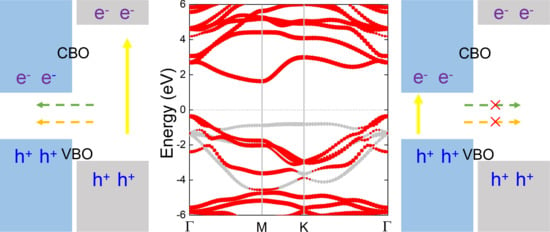
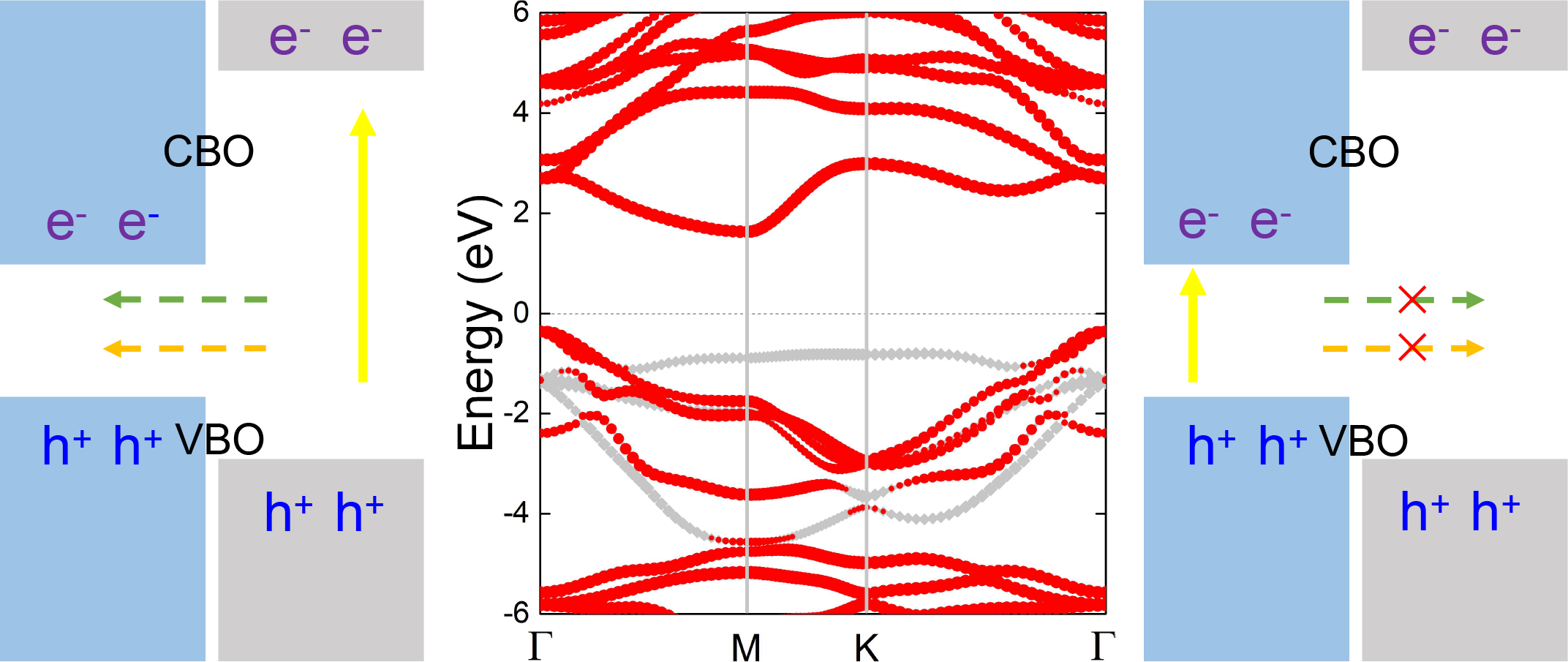
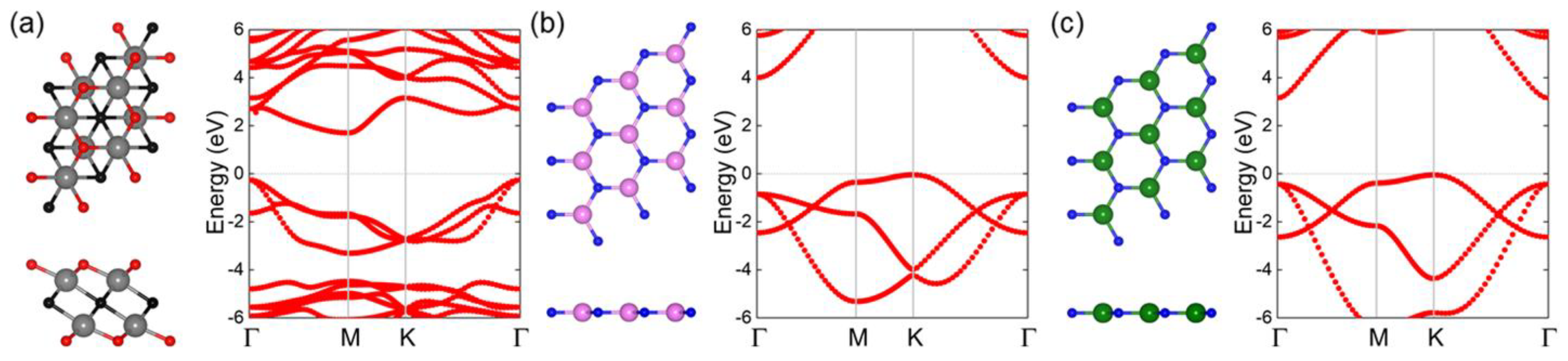
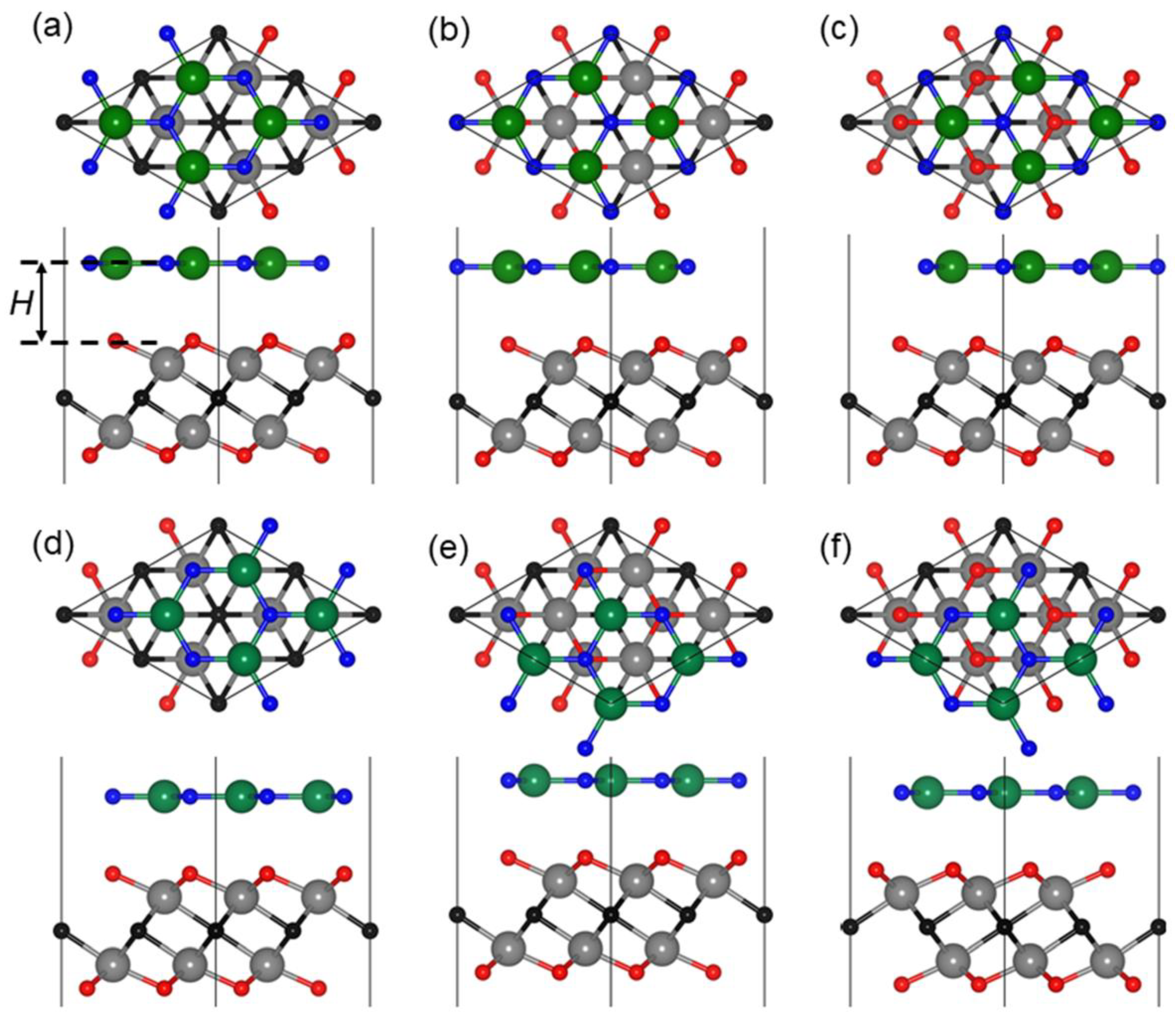
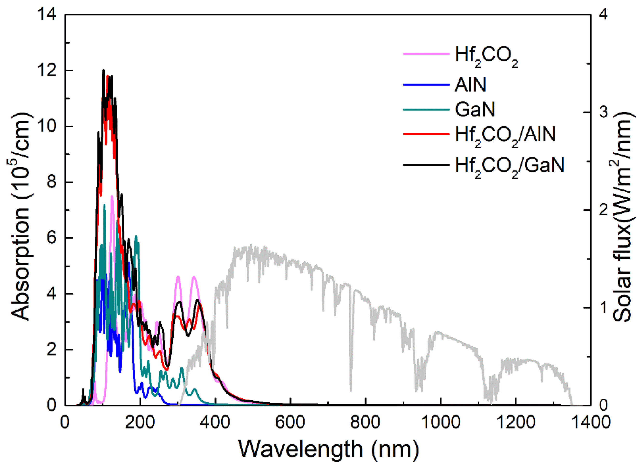
3. Results and Discussions
4. Conclusions
Supplementary Materials
Author Contributions
Funding
Data Availability Statement
Conflicts of Interest
References
- Geim, A.K.; Novoselov, K. The rise of graphene. Nat. Mater. 2007, 6, 183–191. [Google Scholar] [CrossRef]
- Jariwala, D.; Sangwan, V.K.; Lauhon, L.; Marks, T.J.; Hersam, M.C. Carbon nanomaterials for electronics, optoelectronics, photovoltaics, and sensing. Chem. Soc. Rev. 2013, 42, 2824–2860. [Google Scholar] [CrossRef] [Green Version]
- Stoller, M.D.; Park, S.; Zhu, Y.; An, J.; Ruoff, R.S. Graphene-Based Ultracapacitors. Nano Lett. 2008, 8, 3498–3502. [Google Scholar] [CrossRef] [PubMed]
- Wang, J.; Deng, S.; Liu, Z.; Liu, Z. The rare two-dimensional materials with Dirac cones. Natl. Sci. Rev. 2015, 2, 22–39. [Google Scholar] [CrossRef] [Green Version]
- Sun, M.; Tang, W.; Li, S.; Chou, J.-P.; Hu, A.; Schwingenschlögl, U. Molecular doping of blue phosphorene: A first-principles investigation. J. Phys. Condens. Matter 2019, 32, 055501. [Google Scholar] [CrossRef] [Green Version]
- Sun, M.; Schwingenschlögl, U. Unique Omnidirectional Negative Poisson’s Ratio in δ-Phase Carbon Monochalcogenides. J. Phys. Chem. C 2021, 125, 4133–4138. [Google Scholar] [CrossRef]
- Sun, M.; Schwingenschlögl, U. δ-CS: A Direct-Band-Gap Semiconductor Combining Auxeticity, Ferroelasticity, and Potential for High-Efficiency Solar Cells. Phys. Rev. Appl. 2020, 14, 044015. [Google Scholar] [CrossRef]
- Palummo, M.; Bernardi, M.; Grossman, J.C. Exciton Radiative Lifetimes in Two-Dimensional Transition Metal Dichalcogenides. Nano Lett. 2015, 15, 2794–2800. [Google Scholar] [CrossRef] [Green Version]
- Bernardi, M.; Palummo, M.; Grossman, J.C. Semiconducting Monolayer Materials as a Tunable Platform for Excitonic Solar Cells. ACS Nano 2012, 6, 10082–10089. [Google Scholar] [CrossRef] [Green Version]
- Chen, H.-Y.; Palummo, M.; Sangalli, D.; Bernardi, M. Theory and Ab Initio Computation of the Anisotropic Light Emission in Monolayer Transition Metal Dichalcogenides. Nano Lett. 2018, 18, 3839–3843. [Google Scholar] [CrossRef] [Green Version]
- Sun, M.; Luo, Y.; Yan, Y.; Schwingenschlögl, U. Ultrahigh Carrier Mobility in the Two-Dimensional Semiconductors B8Si4, B8Ge4, and B8Sn4. Chem. Mater. 2021, 33, 6475–6483. [Google Scholar] [CrossRef]
- Novoselov, K.S.; Geim, A.K.; Morozov, S.V.; Jiang, D.; Zhang, Y.; Dubonos, S.V.; Grigorieva, I.V.; Firsov, A.A. Electric Field Effect in Atomically Thin Carbon Films. Science 2004, 306, 666–669. [Google Scholar] [CrossRef] [Green Version]
- Butler, S.Z.; Hollen, S.; Cao, L.; Cui, Y.; Gupta, J.A.; Gutiérrez, H.R.; Heinz, T.F.; Hong, S.S.; Huang, J.; Ismach, A.F.; et al. Progress, Challenges, and Opportunities in Two-Dimensional Materials Beyond Graphene. ACS Nano 2013, 7, 2898–2926. [Google Scholar] [CrossRef]
- Zheng, Z.; Ren, K.; Huang, Z.; Zhu, Z.; Wang, K.; Shen, Z.; Yu, J. Remarkably improved Curie temperature for two-dimensional CrI3 by gas molecular adsorption: A DFT study. Semicond. Sci. Technol. 2021, 36, 075015. [Google Scholar] [CrossRef]
- Sun, M.; Yan, Y.; Schwingenschlögl, U. Beryllene: A Promising Anode Material for Na- and K-Ion Batteries with Ultrafast Charge/Discharge and High Specific Capacity. J. Phys. Chem. Lett. 2020, 11, 9051–9056. [Google Scholar] [CrossRef]
- Sun, M.; Chou, J.-P.; Hu, A.; Schwingenschlögl, U. Point Defects in Blue Phosphorene. Chem. Mater. 2019, 31, 8129–8135. [Google Scholar] [CrossRef]
- Sun, M.; Schwingenschlögl, U. Structure Prototype Outperforming MXenes in Stability and Performance in Metal-Ion Batteries: A High Throughput Study. Adv. Energy Mater. 2021, 11, 2003633. [Google Scholar] [CrossRef]
- Li, L.; Yu, Y.; Ye, G.J.; Ge, Q.; Ou, X.; Wu, H.; Feng, D.; Chen, X.H.; Zhang, Y. Black phosphorus field-effect transistors. Nat. Nanotechnol. 2014, 9, 372–377. [Google Scholar] [CrossRef] [PubMed] [Green Version]
- Wu, J.; Mao, N.; Xie, L.; Xu, H.; Zhang, J. Identifying the Crystalline Orientation of Black Phosphorus Using Angle-Resolved Polarized Raman Spectroscopy. Angew. Chem. Int. Ed. 2015, 54, 2366–2369. [Google Scholar] [CrossRef] [PubMed]
- Li, Y.; Yang, S.; Li, J. Modulation of the Electronic Properties of Ultrathin Black Phosphorus by Strain and Electrical Field. J. Phys. Chem. C 2014, 118, 23970–23976. [Google Scholar] [CrossRef]
- Hong, T.; Chamlagain, B.; Lin, W.; Chuang, H.-J.; Pan, M.; Zhou, Z.; Xu, Y.-Q. Polarized photocurrent response in black phosphorus field-effect transistors. Nanoscale 2014, 6, 8978–8983. [Google Scholar] [CrossRef] [PubMed]
- Zhang, S.; Yan, Z.; Shengli, Z.; Chen, Z.; Zeng, H. Atomically Thin Arsenene and Antimonene: Semimetal-Semiconductor and Indirect-Direct Band-Gap Transitions. Angew. Chem. Int. Ed. 2015, 54, 3112–3115. [Google Scholar] [CrossRef] [PubMed]
- Shu, H.; Li, Y.; Niu, X.; Guo, J. Electronic structures and optical properties of arsenene and antimonene under strain and an electric field. J. Mater. Chem. C 2017, 6, 83–90. [Google Scholar] [CrossRef]
- Xu, Y.; Peng, B.; Zhang, H.; Shao, H.; Zhang, R.; Zhu, H. First-principle calculations of optical properties of monolayer arsenene and antimonene allotropes. Ann. Phys. 2017, 529. [Google Scholar] [CrossRef] [Green Version]
- Ersan, F.; Akturk, E.; Ciraci, S. Interaction of Adatoms and Molecules with Single-Layer Arsenene Phases. J. Phys. Chem. C 2016, 120, 14345–14355. [Google Scholar] [CrossRef]
- Dong, M.M.; He, C.; Zhang, W.X. Tunable Electronic Properties of Arsenene and Transition-Metal Dichalcogenide Heterostructures: A First-Principles Calculation. J. Phys. Chem. C 2017, 121, 22040–22048. [Google Scholar] [CrossRef]
- Kamal, C.; Ezawa, M. Arsenene: Two-dimensional buckled and puckered honeycomb arsenic systems. Phys. Rev. B 2015, 91. [Google Scholar] [CrossRef] [Green Version]
- Mogulkoc, Y.; Modarresi, M.; Mogulkoc, A.; Ciftci, Y. Electronic and optical properties of bilayer blue phosphorus. Comput. Mater. Sci. 2016, 124, 23–29. [Google Scholar] [CrossRef] [Green Version]
- Sun, H.; Liu, G.; Li, Q.; Wan, X. First-principles study of thermal expansion and thermomechanics of single-layer black and blue phosphorus. Phys. Lett. A 2016, 380, 2098–2104. [Google Scholar] [CrossRef]
- Mogulkoc, Y.; Modarresi, M.; Mogulkoc, A.; Alkan, B. Electronic and optical properties of boron phosphide/blue phosphorus heterostructures. Phys. Chem. Chem. Phys. 2018, 20, 12053–12060. [Google Scholar] [CrossRef]
- Sun, M.; Hao, Y.; Ren, Q.; Zhao, Y.; Du, Y.; Tang, W. Tuning electronic and magnetic properties of blue phosphorene by doping Al, Si, As and Sb atom: A DFT calculation. Solid State Commun. 2016, 242, 36–40. [Google Scholar] [CrossRef]
- Tsai, D.-S.; Liu, K.-K.; Lien, D.-H.; Tsai, M.-L.; Kang, C.-F.; Lin, C.-A.; Li, L.-J.; He, J.-H. Few-Layer MoS2with High Broadband Photogain and Fast Optical Switching for Use in Harsh Environments. ACS Nano 2013, 7, 3905–3911. [Google Scholar] [CrossRef] [PubMed]
- Wang, J.; Shu, H.; Zhao, T.; Liang, P.; Wang, N.; Cao, D.; Chen, X. Intriguing electronic and optical properties of two-dimensional Janus transition metal dichalcogenides. Phys. Chem. Chem. Phys. 2018, 20, 18571–18578. [Google Scholar] [CrossRef]
- Ma, X.; Wu, X.; Wang, H.; Wang, Y. A Janus MoSSe monolayer: A potential wide solar-spectrum water-splitting photocatalyst with a low carrier recombination rate. J. Mater. Chem. A 2018, 6, 2295–2301. [Google Scholar] [CrossRef]
- Liao, C.; Tang, L.; Wang, L.; Li, Y.; Xu, J.; Jia, Y. Low-threshold near-infrared lasing at room temperature using low-toxicity Ag2Se quantum dots. Nanoscale 2020, 12, 21879–21884. [Google Scholar] [CrossRef] [PubMed]
- Jiang, D.; Ni, C.; Tang, W.; Xiang, N. Numerical simulation of elasto-inertial focusing of particles in straight microchannels. J. Phys. D Appl. Phys. 2021, 54, 065401. [Google Scholar] [CrossRef]
- Sun, M.; Schwingenschlögl, U. B2P6: A Two-Dimensional Anisotropic Janus Material with Potential in Photocatalytic Water Splitting and Metal-Ion Batteries. Chem. Mater. 2020, 32, 4795–4800. [Google Scholar] [CrossRef]
- Wang, S.; Ren, C.; Tian, H.; Yu, J.; Sun, M. MoS2/ZnO van der Waals heterostructure as a high-efficiency water splitting photocatalyst: A first-principles study. Phys. Chem. Chem. Phys. 2018, 20, 13394–13399. [Google Scholar] [CrossRef]
- Kumar, R.; Das, D.; Singh, A.K. C2N/WS2 van der Waals type-II heterostructure as a promising water splitting photocatalyst. J. Catal. 2018, 359, 143–150. [Google Scholar] [CrossRef]
- Gong, Y.; Lin, J.; Wang, X.; Shi, G.; Lei, S.; Lin, Z.; Zou, X.; Ye, G.; Vajtai, R.; Yakobson, B.I.; et al. Vertical and in-plane heterostructures from WS2/MoS2 monolayers. Nat. Mater. 2014, 13, 1135–1142. [Google Scholar] [CrossRef] [Green Version]
- Zhang, Z.; Zhang, Y.; Xie, Z.; Wei, X.; Guo, T.; Fan, J.; Ni, L.; Tian, Y.; Liu, J.; Duan, L. Tunable electronic properties of an Sb/InSe van der Waals heterostructure by electric field effects. Phys. Chem. Chem. Phys. 2019, 21, 5627–5633. [Google Scholar] [CrossRef] [PubMed]
- Ren, K.; Tang, W.; Sun, M.; Cai, Y.; Cheng, Y.; Zhang, G. A direct Z-scheme PtS2/arsenene van der Waals heterostructure with high photocatalytic water splitting efficiency. Nanoscale 2020, 12, 17281–17289. [Google Scholar] [CrossRef]
- Ren, K.; Sun, M.; Luo, Y.; Wang, S.; Yu, J.; Tang, W. First-principle study of electronic and optical properties of two-dimensional materials-based heterostructures based on transition metal dichalcogenides and boron phosphide. Appl. Surf. Sci. 2019, 476, 70–75. [Google Scholar] [CrossRef]
- Ren, K.; Wang, S.; Luo, Y.; Xu, Y.; Sun, M.; Yu, J.; Tang, W. Strain-enhanced properties of van der Waals heterostructure based on blue phosphorus and g-GaN as a visible-light-driven photocatalyst for water splitting. RSC Adv. 2019, 9, 4816–4823. [Google Scholar] [CrossRef] [Green Version]
- Ren, K.; Wang, K.; Cheng, Y.; Tang, W.; Zhang, G. Two-dimensional heterostructures for photocatalytic water splitting: A review of recent progress. Nano Futur. 2020, 4, 032006. [Google Scholar] [CrossRef]
- Li, J.; Huang, Z.; Ke, W.; Yu, J.; Ren, K.; Dong, Z. High solar-to-hydrogen efficiency in Arsenene/GaX (X = S, Se) van der Waals heterostructure for photocatalytic water splitting. J. Alloy. Compd. 2021, 866, 158774. [Google Scholar] [CrossRef]
- Din, H.U.; Idrees, M.; Rehman, G.; Nguyen, C.V.; Gan, L.-Y.; Ahmad, I.; Maqbool, M.; Amin, B. Electronic structure, optical and photocatalytic performance of SiC–MX2 (M = Mo, W and X = S, Se) van der Waals heterostructures. Phys. Chem. Chem. Phys. 2018, 20, 24168–24175. [Google Scholar] [CrossRef]
- Williams, K.R.; Diroll, B.T.; Watkins, N.E.; Rui, X.; Brumberg, A.; Klie, R.F.; Schaller, R.D. Synthesis of Type I PbSe/CdSe Dot-on-Plate Heterostructures with Near-Infrared Emission. J. Am. Chem. Soc. 2019, 141, 5092–5096. [Google Scholar] [CrossRef]
- Zheng, W.; Zheng, B.; Jiang, Y.; Yan, C.; Chen, S.; Liu, Y.; Sun, X.; Zhu, C.; Qi, Z.; Yang, T.; et al. Probing and Manipulating Carrier Interlayer Diffusion in van der Waals Multilayer by Constructing Type-I Heterostructure. Nano Lett. 2019, 19, 7217–7225. [Google Scholar] [CrossRef] [PubMed]
- Bellus, M.; Li, M.; Lane, S.; Ceballos, F.; Cui, Q.; Zeng, X.C.; Zhao, H. Type-I van der Waals heterostructure formed by MoS2 and ReS2 monolayers. Nanoscale Horiz. 2016, 2, 31–36. [Google Scholar] [CrossRef] [PubMed]
- Dorfs, D.; Franzl, T.; Osovsky, R.; Brumer, M.; Lifshitz, E.; Klar, T.; Eychmüller, A. Type-I and Type-II Nanoscale Heterostructures Based on CdTe Nanocrystals: A Comparative Study. Small 2008, 4, 1148–1152. [Google Scholar] [CrossRef]
- Lei, J.-C.; Zhang, X.; Zhou, Z. Recent advances in MXene: Preparation, properties, and applications. Front. Phys. 2015, 10, 276–286. [Google Scholar] [CrossRef]
- Jiang, Q.; Lei, Y.; Liang, H.; Xi, K.; Xia, C.; Alshareef, H.N. Review of MXene electrochemical microsupercapacitors. Energy Storage Mater. 2020, 27, 78–95. [Google Scholar] [CrossRef]
- Ling, Z.; Ren, C.E.; Zhao, M.-Q.; Yang, J.; Giammarco, J.M.; Qiu, J.; Barsoum, M.W.; Gogotsi, Y. Flexible and conductive MXene films and nanocomposites with high capacitance. Proc. Natl. Acad. Sci. USA 2014, 111, 16676–16681. [Google Scholar] [CrossRef] [PubMed] [Green Version]
- Naguib, M.; Come, J.; Dyatkin, B.; Presser, V.; Taberna, P.-L.; Simon, P.; Barsoum, M.W.; Gogotsi, Y. MXene: A promising transition metal carbide anode for lithium-ion batteries. Electrochem. Commun. 2012, 16, 61–64. [Google Scholar] [CrossRef] [Green Version]
- Wang, S.; Li, B.; Li, L.; Tian, Z.; Zhang, Q.; Chen, L.; Zeng, X.C. Highly efficient N2 fixation catalysts: Transition-metal carbides M2C (MXenes). Nanoscale 2019, 12, 538–547. [Google Scholar] [CrossRef] [PubMed]
- Xiao, R.; Zhao, C.; Zou, Z.; Chen, Z.; Tian, L.; Xu, H.; Tang, H.; Liu, Q.; Lin, Z.; Yang, X. In situ fabrication of 1D CdS nanorod/2D Ti3C2 MXene nanosheet Schottky heterojunction toward enhanced photocatalytic hydrogen evolution. Appl. Catal. B: Environ. 2019, 268, 118382. [Google Scholar] [CrossRef]
- Zhang, X.; Zhang, Z.; Zhou, Z. MXene-based materials for electrochemical energy storage. J. Energy Chem. 2018, 27, 73–85. [Google Scholar] [CrossRef] [Green Version]
- Khazaei, M.; Arai, M.; Sasaki, T.; Chung, C.-Y.; Venkataramanan, N.S.; Estili, M.; Sakka, Y.; Kawazoe, Y. Novel Electronic and Magnetic Properties of Two-Dimensional Transition Metal Carbides and Nitrides. Adv. Funct. Mater. 2012, 23, 2185–2192. [Google Scholar] [CrossRef]
- Zhan, X.; Si, C.; Zhou, J.; Sun, Z. MXene and MXene-based composites: Synthesis, properties and environment-related applications. Nanoscale Horiz. 2019, 5, 235–258. [Google Scholar] [CrossRef]
- He, J.; Ding, G.; Zhong, C.; Li, S.; Li, D.; Zhang, G. Cr2TiC2-based double MXenes: Novel 2D bipolar antiferromagnetic semiconductor with gate-controllable spin orientation toward antiferromagnetic spintronics. Nanoscale 2018, 11, 356–364. [Google Scholar] [CrossRef] [PubMed]
- Zhu, B.; Zhang, F.; Qiu, J.; Chen, X.; Zheng, K.; Guo, H.; Yu, J.; Bao, J. A novel Hf2CO2/WS2 van der Waals heterostructure as a potential candidate for overall water splitting photocatalyst. Mater. Sci. Semicond. Process. 2021, 133, 105947. [Google Scholar] [CrossRef]
- Gandi, A.N.; Alshareef, H.N.; Schwingenschlögl, U. Thermoelectric Performance of the MXenes M2CO2 (M = Ti, Zr, or Hf). Chem. Mater. 2016, 28, 1647–1652. [Google Scholar] [CrossRef] [Green Version]
- Sharma, V.; Kumar, A.; Krishnan, V. Two-dimensional MXene-based heterostructures for photocatalysis. In Handbook of Smart Photocatalytic Materials; Elsevier: Amsterdam, The Netherlands, 2020; pp. 247–267. [Google Scholar] [CrossRef]
- Guo, Z.; Miao, N.; Zhou, J.; Sa, B.; Sun, Z. Strain-mediated type-I/type-II transition in MXene/Blue phosphorene van der Waals heterostructures for flexible optical/electronic devices. J. Mater. Chem. C 2016, 5, 978–984. [Google Scholar] [CrossRef]
- Fu, C.-F.; Li, X.; Luo, Q.; Yang, J. Two-dimensional multilayer M2CO2(M = Sc, Zr, Hf) as photocatalysts for hydrogen production from water splitting: A first principles study. J. Mater. Chem. A 2017, 5, 24972–24980. [Google Scholar] [CrossRef]
- Li, S.; Li, X.; Zhang, R.; Cui, H. Strain-tunable electronic properties and optical properties of Hf2CO2 MXene. Int. J. Quantum Chem. 2020, 120. [Google Scholar] [CrossRef]
- Wang, Y.; Ma, S.; Wang, L.; Jiao, Z. A novel highly selective and sensitive NH3 gas sensor based on monolayer Hf2CO2. Appl. Surf. Sci. 2019, 492, 116–124. [Google Scholar] [CrossRef]
- Bacaksiz, C.; Sahin, H.; Ozaydin, H.D.; Horzum, S.; Senger, T.; Peeters, F.M. Hexagonal AlN: Dimensional-crossover-driven band-gap transition. Phys. Rev. B 2015, 91, 085430. [Google Scholar] [CrossRef] [Green Version]
- Bai, Y.; Deng, K.; Kan, E. Electronic and magnetic properties of an AlN monolayer doped with first-row elements: A first-principles study. RSC Adv. 2015, 5, 18352–18358. [Google Scholar] [CrossRef]
- Zhang, C.-W. First-principles study on electronic structures and magnetic properties of AlN nanosheets and nanoribbons. J. Appl. Phys. 2012, 111, 43702. [Google Scholar] [CrossRef]
- Zhang, C.-W.; Zheng, F.-B. First-principles prediction on electronic and magnetic properties of hydrogenated AlN nanosheets. J. Comput. Chem. 2011, 32, 3122–3128. [Google Scholar] [CrossRef]
- Xu, C.; Xue, L.; Yin, C.; Wang, G. Formation and photoluminescence properties of AlN nanowires. Phys. Status solidi (a) 2003, 198, 329–335. [Google Scholar] [CrossRef]
- Xu, D.; He, H.; Pandey, R.; Karna, S.P. Stacking and electric field effects in atomically thin layers of GaN. J. Phys. Condens. Matter 2013, 25, 345302. [Google Scholar] [CrossRef] [PubMed]
- Chen, Q.; Hu, H.; Chen, X.; Wang, J. Tailoring band gap in GaN sheet by chemical modification and electric field: Ab initio calculations. Appl. Phys. Lett. 2011, 98, 053102. [Google Scholar] [CrossRef]
- Wang, W.; Zheng, Y.; Li, X.; Li, Y.; Zhao, H.; Huang, L.; Yang, Z.; Zhang, X.; Li, G. 2D AlN Layers Sandwiched Between Graphene and Si Substrates. Adv. Mater. 2018, 31, e1803448. [Google Scholar] [CrossRef]
- Taniyasu, Y.; Kasu, M.; Makimoto, T. An aluminium nitride light-emitting diode with a wavelength of 210 nanometres. Nat. Cell Biol. 2006, 441, 325–328. [Google Scholar] [CrossRef]
- Lee, S.; Kim, D.Y. Characteristics of ZnO/GaN heterostructure formed on GaN substrate by sputtering deposition of ZnO. Mater. Sci. Eng. B 2007, 137, 80–84. [Google Scholar] [CrossRef]
- McDermott, E.J.; Kurmaev, E.Z.; Boyko, T.D.; Finkelstein, L.D.; Green, R.J.; Maeda, K.; Domen, K.; Moewes, A. Structural and Band Gap Investigation of GaN:ZnO Heterojunction Solid Solution Photocatalyst Probed by Soft X-ray Spectroscopy. J. Phys. Chem. C 2012, 116, 7694–7700. [Google Scholar] [CrossRef]
- Cui, Z.; Li, E.; Ke, X.; Zhao, T.; Yang, Y.; Ding, Y.; Liu, T.; Qu, Y.; Xu, S. Adsorption of alkali-metal atoms on GaN nanowires photocathode. Appl. Surf. Sci. 2017, 423, 829–835. [Google Scholar] [CrossRef]
- Liao, J.; Sa, B.; Zhou, J.; Ahuja, R.; Sun, Z. Design of High-Efficiency Visible-Light Photocatalysts for Water Splitting: MoS2/AlN(GaN) Heterostructures. J. Phys. Chem. C 2014, 118, 17594–17599. [Google Scholar] [CrossRef]
- Lou, P.; Lee, J.Y. GeC/GaN vdW Heterojunctions: A Promising Photocatalyst for Overall Water Splitting and Solar Energy Conversion. ACS Appl. Mater. Interfaces 2020, 12, 14289–14297. [Google Scholar] [CrossRef]
- Capelle, K. A bird’s-eye view of density-functional theory. Braz. J. Phys. 2006, 36, 1318–1343. [Google Scholar] [CrossRef]
- Grimme, S.; Antony, J.; Ehrlich, S.; Krieg, H. A consistent and accurate ab initio parametrization of density functional dispersion correction (DFT-D) for the 94 elements H-Pu. J. Chem. Phys. 2010, 132, 154104. [Google Scholar] [CrossRef] [PubMed] [Green Version]
- Kresse, G.; Furthmüller, J. Efficiency of ab-initio total energy calculations for metals and semiconductors using a plane-wave basis set. Comput. Mater. Sci. 1996, 6, 15–50. [Google Scholar] [CrossRef]
- Kresse, G.; Furthmüller, J. Efficient iterative schemes for ab initio total-energy calculations using a plane-wave basis set. Phys. Rev. B 1996, 54, 11169–11186. [Google Scholar] [CrossRef] [PubMed]
- Heyd, J.; Peralta, J.; Scuseria, G.E.; Martin, R.L. Energy band gaps and lattice parameters evaluated with the Heyd-Scuseria-Ernzerhof screened hybrid functional. J. Chem. Phys. 2005, 123, 174101. [Google Scholar] [CrossRef]
- Ren, K.; Wang, S.; Luo, Y.; Chou, J.-P.; Yu, J.; Tang, W.; Sun, M. High-efficiency photocatalyst for water splitting: A Janus MoSSe/XN (X = Ga, Al) van der Waals heterostructure. J. Phys. D Appl. Phys. 2020, 53, 185504. [Google Scholar] [CrossRef]
- Singh, A.; Mathew, K.; Zhuang, H.L.; Hennig, R.G. Computational Screening of 2D Materials for Photocatalysis. J. Phys. Chem. Lett. 2015, 6, 1087–1098. [Google Scholar] [CrossRef]
- Voinova, V.V.; Selivanov, N.A.; Plyushchenko, I.V.; Vokuev, M.F.; Bykov, A.Y.; Klyukin, I.N.; Novikov, A.S.; Zhdanov, A.P.; Grigoriev, M.S.; Rodin, I.A.; et al. Fused 1,2-Diboraoxazoles Based on closo-Decaborate Anion–Novel Members of Diboroheterocycle Class. Molecules 2021, 26, 248. [Google Scholar] [CrossRef]
- Adonin, S.A.; Bondarenko, M.A.; Novikov, A.S.; Sokolov, M.N. Halogen Bonding in Isostructural Co(II) Complexes with 2-Halopyridines. Crystals 2020, 10, 289. [Google Scholar] [CrossRef] [Green Version]
- Soldatova, N.S.; Suslonov, V.V.; Kissler, T.Y.; Ivanov, D.M.; Novikov, A.S.; Yusubov, M.S.; Postnikov, P.S.; Kukushkin, V.Y. Halogen Bonding Provides Heterooctameric Supramolecular Aggregation of Diaryliodonium Thiocyanate. Crystals 2020, 10, 230. [Google Scholar] [CrossRef] [Green Version]
- Nenajdenko, V.; Shikhaliyev, N.; Maharramov, A.; Bagirova, K.; Suleymanova, G.; Novikov, A.; Khrustalev, V.; Tskhovrebov, A. Halogenated Diazabutadiene Dyes: Synthesis, Structures, Supramolecular Features, and Theoretical Studies. Molecules 2020, 25, 5013. [Google Scholar] [CrossRef] [PubMed]
- Mikherdov, A.; Novikov, A.; Kinzhalov, M.; Zolotarev, A.; Boyarskiy, V. Intra-/Intermolecular Bifurcated Chalcogen Bonding in Crystal Structure of Thiazole/Thiadiazole Derived Binuclear (Diaminocarbene)PdII Complexes. Crystals 2018, 8, 112. [Google Scholar] [CrossRef] [Green Version]
- Kryukova, M.A.; Sapegin, A.V.; Novikov, A.S.; Krasavin, M.; Ivanov, D.M. New Crystal Forms for Biologically Active Compounds. Part 1: Noncovalent Interactions in Adducts of Nevirapine with XB Donors. Crystals 2019, 9, 71. [Google Scholar] [CrossRef] [Green Version]
- Kryukova, M.A.; Sapegin, A.V.; Novikov, A.S.; Krasavin, M.; Ivanov, D.M. New Crystal Forms for Biologically Active Compounds. Part 2: Anastrozole as N-Substituted 1,2,4-Triazole in Halogen Bonding and Lp-π Interactions with 1,4-Diiodotetrafluorobenzene. Crystals 2020, 10, 371. [Google Scholar] [CrossRef]
- Ostras’, A.S.; Ivanov, D.M.; Novikov, A.S.; Tolstoy, P.M. Phosphine Oxides as Spectroscopic Halogen Bond Descriptors: IR and NMR Correlations with Interatomic Distances and Complexation Energy. Molecules 2020, 25, 1406. [Google Scholar] [CrossRef] [Green Version]
- Bolotin, D.S.; Il’In, M.V.; Suslonov, V.V.; Novikov, A.S. Symmetrical Noncovalent Interactions Br···Br Observed in Crystal Structure of Exotic Primary Peroxide. Symmetry 2020, 12, 637. [Google Scholar] [CrossRef] [Green Version]
- Klyukin, I.; Vlasova, Y.; Novikov, A.; Zhdanov, A.; Zhizhin, K.; Kuznetsov, N. Theoretical Study of closo-Borate Anions [BnHn]2− (n = 5–12): Bonding, Atomic Charges, and Reactivity Analysis. Symmetry 2021, 13, 464. [Google Scholar] [CrossRef]
- Chen, X.; Tian, F.; Persson, C.; Duan, W.; Chen, N.-X. Interlayer interactions in graphites. Sci. Rep. 2013, 3, 3046. [Google Scholar] [CrossRef]
- Björkman, T.; Guļāns, A.; Krasheninnikov, A.; Nieminen, R.M. van der Waals Bonding in Layered Compounds from Advanced Density-Functional First-Principles Calculations. Phys. Rev. Lett. 2012, 108, 235502. [Google Scholar] [CrossRef] [Green Version]
- Nosé, S. A unified formulation of the constant temperature molecular dynamics methods. J. Chem. Phys. 1984, 81, 511–519. [Google Scholar] [CrossRef] [Green Version]
- Tang, W.; Sanville, E.; Henkelman, G. A grid-based Bader analysis algorithm without lattice bias. J. Phys. Condens. Matter 2009, 21, 084204. [Google Scholar] [CrossRef] [PubMed]
- Bernardi, M.; Palummo, M.; Grossman, J.C. Extraordinary Sunlight Absorption and One Nanometer Thick Photovoltaics Using Two-Dimensional Monolayer Materials. Nano Lett. 2013, 13, 3664–3670. [Google Scholar] [CrossRef] [PubMed]
- Bruno, M.; Palummo, M.; Marini, A.; Del Sole, R.; Ossicini, S. From Si Nanowires to Porous Silicon: The Role of Excitonic Effects. Phys. Rev. Lett. 2007, 98, 036807. [Google Scholar] [CrossRef] [PubMed] [Green Version]


| a | BHf–C | BHf–O | BM–N | Ebinding | H | Eg | |
|---|---|---|---|---|---|---|---|
| Hf2CO2 | 3.363 | 2.369 | 2.132 | 1.820 | |||
| AlN | 3.127 | 1.805 | 4.042 | ||||
| GaN | 3.283 | 1.895 | 3.203 | ||||
| Hf2CO2/AlN | 3.328 | 2.354 | 2.121 | 1.922 | −56.98 | 1.924 | 1.826 |
| Hf2CO2/GaN | 3.329 | 2.355 | 2.101 | 1.922 | −52.44 | 2.235 | 1.734 |
Publisher’s Note: MDPI stays neutral with regard to jurisdictional claims in published maps and institutional affiliations. |
© 2021 by the authors. Licensee MDPI, Basel, Switzerland. This article is an open access article distributed under the terms and conditions of the Creative Commons Attribution (CC BY) license (https://creativecommons.org/licenses/by/4.0/).
Share and Cite
Ren, K.; Zheng, R.; Xu, P.; Cheng, D.; Huo, W.; Yu, J.; Zhang, Z.; Sun, Q. Electronic and Optical Properties of Atomic-Scale Heterostructure Based on MXene and MN (M = Al, Ga): A DFT Investigation. Nanomaterials 2021, 11, 2236. https://0-doi-org.brum.beds.ac.uk/10.3390/nano11092236
Ren K, Zheng R, Xu P, Cheng D, Huo W, Yu J, Zhang Z, Sun Q. Electronic and Optical Properties of Atomic-Scale Heterostructure Based on MXene and MN (M = Al, Ga): A DFT Investigation. Nanomaterials. 2021; 11(9):2236. https://0-doi-org.brum.beds.ac.uk/10.3390/nano11092236
Chicago/Turabian StyleRen, Kai, Ruxin Zheng, Peng Xu, Dong Cheng, Wenyi Huo, Jin Yu, Zhuoran Zhang, and Qingyun Sun. 2021. "Electronic and Optical Properties of Atomic-Scale Heterostructure Based on MXene and MN (M = Al, Ga): A DFT Investigation" Nanomaterials 11, no. 9: 2236. https://0-doi-org.brum.beds.ac.uk/10.3390/nano11092236