
Stress Effects on Temperature-Dependent In-Plane Raman Modes of Supported Monolayer Graphene Induced by Thermal Annealing

 , and
, and
Abstract
:
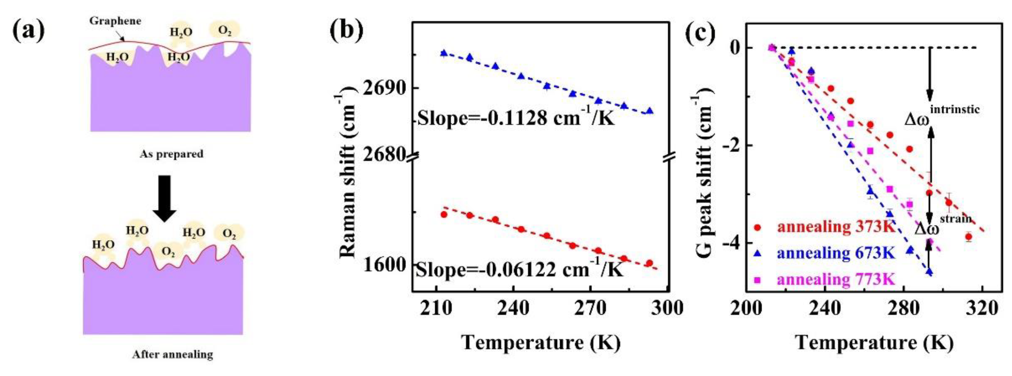
1. Introduction
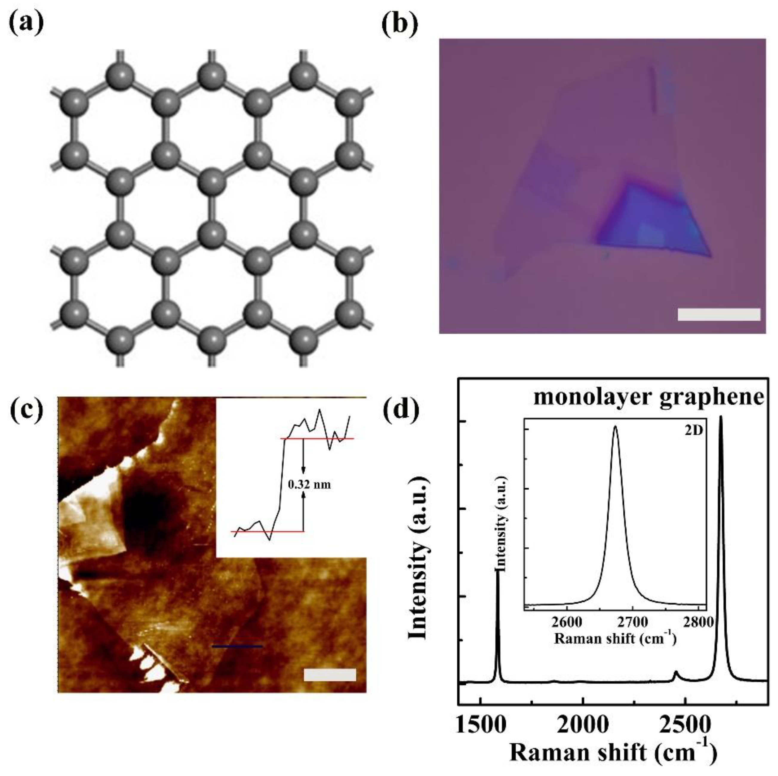
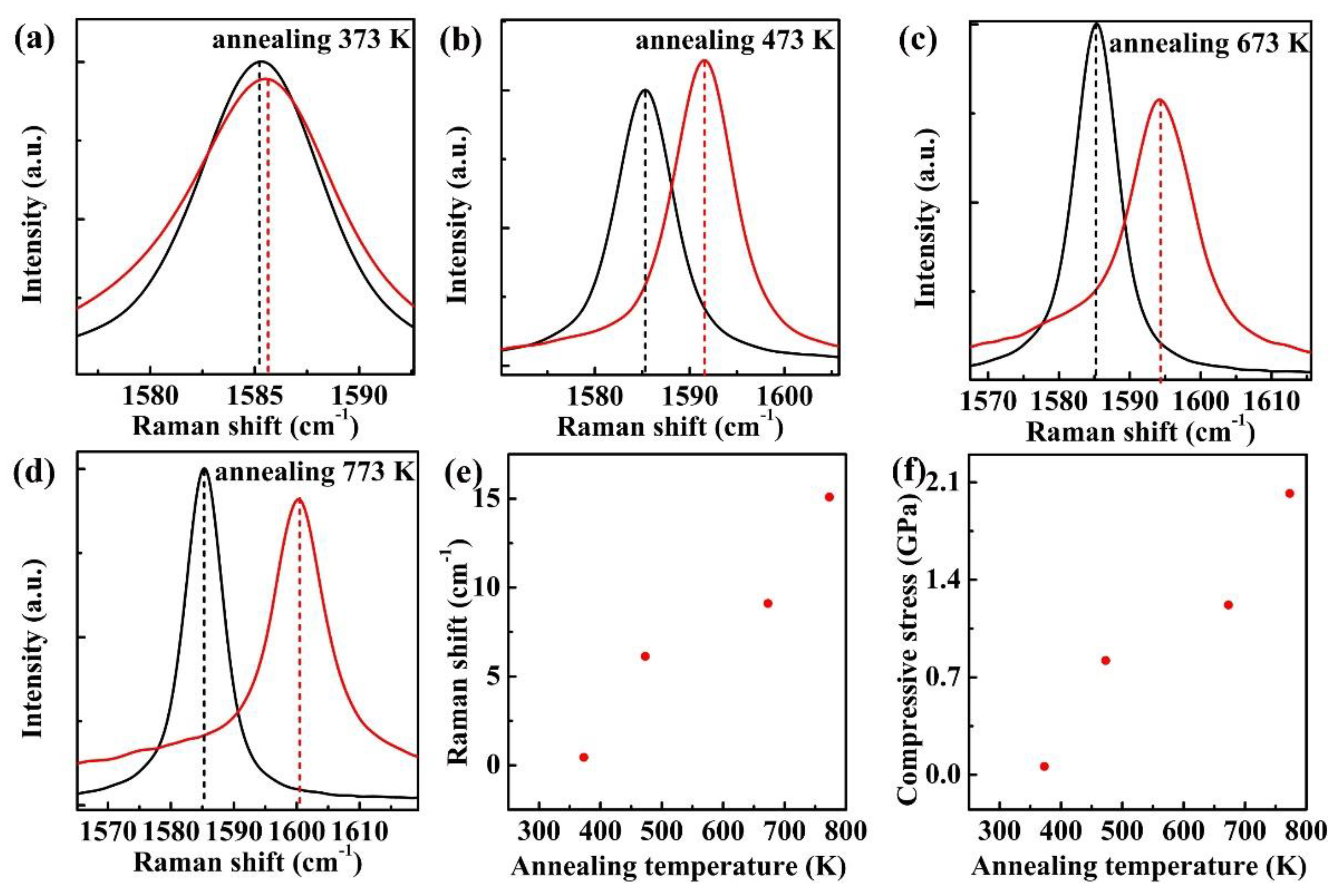
2. Materials and Methods
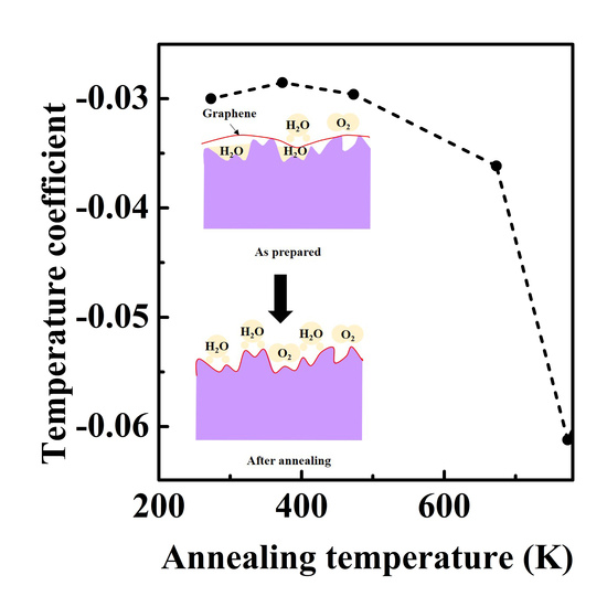
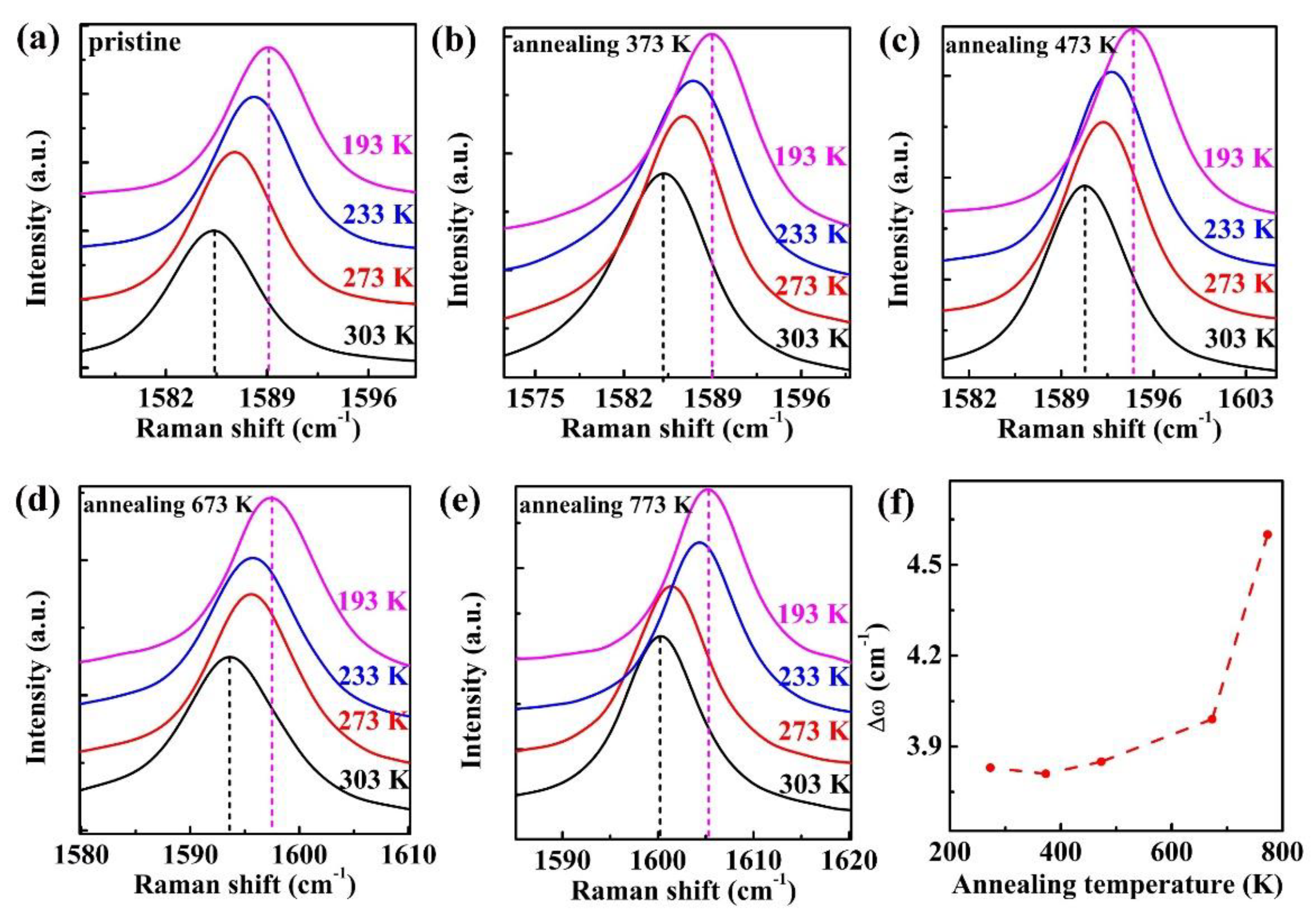
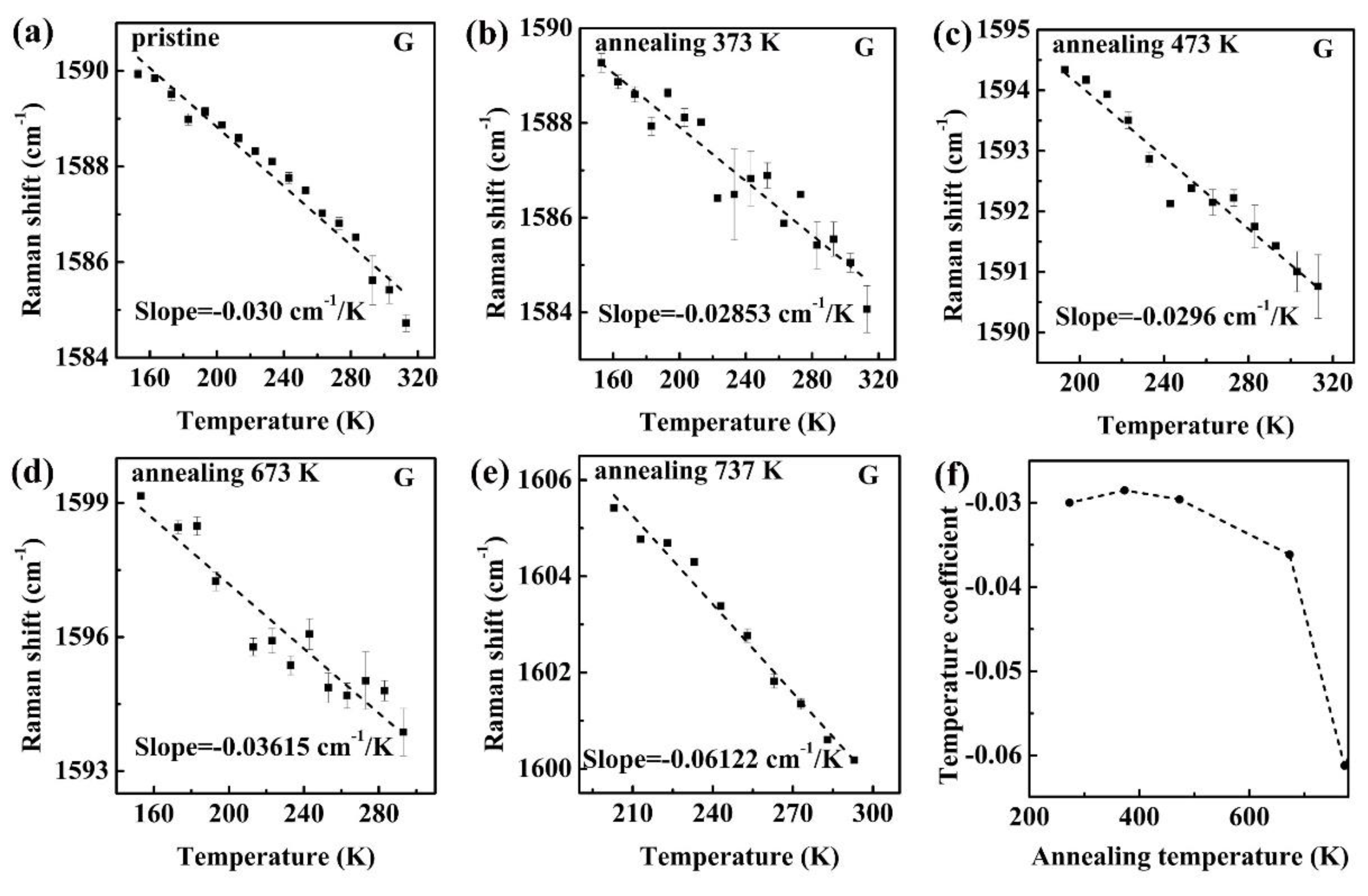
3. Results and Discussion
4. Conclusions
Supplementary Materials
Author Contributions
Funding
Data Availability Statement
Conflicts of Interest
References
- Balandin, A.A. Thermal properties of graphene and nanostructured carbon materials. Nat. Mater. 2011, 10, 569–581. [Google Scholar] [CrossRef] [PubMed] [Green Version]
- Wei, Y.; Zhang, R.; Zhang, Y.; Zheng, X.; Cai, W.; Ge, Q.; Novoselov, K.S.; Xu, Z.; Jiang, T.; Deng, C.; et al. Thickness-independent energy dissipation in Graphene electronics. ACS Appl. Mater. Interfaces 2020, 12, 17706–17712. [Google Scholar] [CrossRef] [PubMed]
- DaSilva, A.M.; Zou, K.; Jain, J.K.; Zhu, J. Mechanism for current saturation and energy dissipation in Graphene transistors. Phys. Rev. Lett. 2010, 104, 236601. [Google Scholar] [CrossRef] [PubMed] [Green Version]
- Zheng, X.; Wei, Y.; Deng, C.; Huang, H.; Yu, Y.; Wang, G.; Peng, G.; Zhu, Z.; Zhang, Y.; Jiang, T.; et al. Controlled layer-by-layer oxidation of MoTe2 via O3 exposure. ACS Appl. Mater. Interfaces 2018, 10, 30045–30050. [Google Scholar] [CrossRef] [PubMed] [Green Version]
- Zheng, X.; Wei, Y.; Liu, J.; Wang, S.; Shi, J.; Yang, H.; Peng, G.; Deng, C.; Luo, W.; Zhao, Y.; et al. A homogeneous p–n junction diode by selective doping of few layer MoSe2 using ultraviolet ozone for high-performance photovoltaic devices. Nanoscale 2019, 11, 13469–13476. [Google Scholar] [CrossRef] [Green Version]
- Zheng, X.; Zhang, X.; Wei, Y.; Liu, J.; Yang, H.; Zhang, X.; Wang, S.; Xie, H.; Deng, C.; Gao, Y.; et al. Enormous enhancement in electrical performance of few-layered MoTe2 due to Schottky barrier reduction induced by ultraviolet ozone treatment. Nano Res. 2020, 13, 952–958. [Google Scholar] [CrossRef]
- Wei, Y.; Deng, C.; Zheng, X.; Chen, Y.; Zhang, X.; Luo, W.; Zhang, Y.; Peng, G.; Liu, J.; Huang, H.; et al. Anisotropic in-plane thermal conductivity for multi-layer WTe2. Nano Res. 2021. [Google Scholar] [CrossRef]
- Pop, E. Energy dissipation and transport in nanoscale devices. Nano Res. 2010, 3, 147–169. [Google Scholar] [CrossRef] [Green Version]
- Yalon, E.; McClellan, C.J.; Smithe, K.K.H.; Muñoz Rojo, M.; Xu, R.L.; Suryavanshi, S.V.; Gabourie, A.J.; Neumann, C.M.; Xiong, F.; Farimani, A.B.; et al. Energy dissipation in monolayer MoS2 electronics. Nano Lett. 2017, 17, 3429–3433. [Google Scholar] [CrossRef] [Green Version]
- Ali, F.; Ahmed, F.; Yang, Z.; Moon, I.; Lee, M.; Hassan, Y.; Lee, C.; Yoo, W.J. Energy dissipation in black phosphorus heterostructured devices. Adv. Mater. Interfaces 2019, 6, 1801528. [Google Scholar] [CrossRef]
- Thripuranthaka, M.; Late, D.J. Temperature dependent phonon shifts in single-layer WS2. ACS Appl. Mater. Interfaces 2014, 6, 1158–1163. [Google Scholar]
- Li, Z.; Wang, Y.; Jiang, J.; Liang, Y.; Zhong, B.; Zhang, H.; Yu, K.; Kan, G.; Zou, M. Temperature-dependent Raman spectroscopy studies of 1–5-layer WSe2. Nano Res. 2020, 13, 591–595. [Google Scholar] [CrossRef]
- Yasaei, P.; Hemmat, Z.; Foss, C.J.; Li, S.J.; Hong, L.; Behranginia, A.; Majidi, L.; Klie, R.F.; Barsoum, M.W.; Aksamija, Z.; et al. Enhanced thermal boundary conductance in few-layer Ti3C2 MXene with encapsulation. Adv. Mater. 2018, 30, 1801629. [Google Scholar] [CrossRef]
- Hemmat, Z.; Yasaei, P.; Schultz, J.F.; Hong, L.; Majidi, L.; Behranginia, A.; Verger, L.; Jiang, N.; Barsoum, M.W.; Klie, R.F.; et al. Tuning thermal transport through atomically thin Ti3C2Tz MXene by current annealing in vacuum. Adv. Funct. Mater. 2019, 29, 1805693. [Google Scholar] [CrossRef]
- Kim, H.G.; Kihm, K.D.; Lee, W.; Lim, G.; Cheon, S.; Lee, W.; Pyun, K.R.; Ko, S.H.; Shin, S. Effect of graphene-substrate conformity on the in-plane thermal conductivity of supported graphene. Carbon 2017, 125, 39–48. [Google Scholar] [CrossRef]
- Ni, Z.H.; Wang, H.M.; Ma, Y.; Kasim, J.; Wu, Y.H.; Shen, Z.X. Tunable stress and controlled thickness modification in Graphene by annealing. ACS Nano 2008, 2, 1033–1039. [Google Scholar] [CrossRef] [Green Version]
- Maiti, A.; Svizhenko, A.; Anantram, M.P. Electronic Transport through carbon nanotubes: Effects of structural deformation and tube chirality. Phys. Rev. Lett. 2002, 88, 126805. [Google Scholar] [CrossRef] [Green Version]
- Zhang, J.; Hong, Y.; Liu, M.; Yue, Y.; Xiong, Q.; Lorenzini, G. Molecular dynamics simulation of the interfacial thermal resistance between phosphorene and silicon substrate. Int. J. Heat Mass Transf. 2017, 104, 871–877. [Google Scholar] [CrossRef]
- Late, D.J.; Shirodkar, S.N.; Waghmare, U.V.; Dravid, V.P.; Rao, C.N.R. Thermal expansion, anharmonicity and temperature-dependent Raman Spectra of single- and few-layer MoSe2 and WSe2. ChemPhysChem 2014, 15, 1592–1598. [Google Scholar] [CrossRef] [PubMed]
- Najmaei, S.; Ajayan, P.M.; Lou, J. Quantitative analysis of the temperature dependency in Raman active vibrational modes of molybdenum disulfide atomic layers. Nanoscale 2013, 5, 9758–9763. [Google Scholar] [CrossRef] [PubMed]
- Huang, X.; Gao, Y.; Yang, T.; Ren, W.; Cheng, H.-M.; Lai, T. Quantitative analysis of temperature dependence of Raman shift of monolayer WS2. Sci. Rep. 2016, 6, 32236. [Google Scholar] [CrossRef] [Green Version]
- Engel, M.; Steiner, M.; Han, S.-J.; Avouris, P. Power dissipation and electrical breakdown in black phosphorus. Nano Lett. 2015, 15, 6785–6788. [Google Scholar] [CrossRef] [PubMed] [Green Version]
- Behranginia, A.; Hemmat, Z.; Majee, A.K.; Foss, C.J.; Yasaei, P.; Aksamija, Z.; Salehi-Khojin, A. Power dissipation of WSe2 field-effect transistors probed by low-frequency Raman thermometry. ACS Appl. Mater. Interfaces 2018, 10, 24892–24898. [Google Scholar] [CrossRef] [PubMed]
- Kim, D.; Kim, H.; Yun, W.S.; Watanabe, K.; Taniguchi, T.; Rho, H.; Bae, M.-H. Energy dissipation mechanism revealed by spatially resolved Raman thermometry of graphene/hexagonal boron nitride heterostructure devices. 2D Mater. 2018, 5, 025009. [Google Scholar] [CrossRef] [Green Version]
- Geim, A.K.; Novoselov, K.S. The rise of graphene. Nanosci. Technol. 2010, 11–19. [Google Scholar] [CrossRef]
- Ni, Z.H.; Yu, T.; Lu, Y.H.; Wang, Y.Y.; Feng, Y.P.; Shen, Z.X. Uniaxial strain on Graphene: Raman Spectroscopy study and band-gap opening. ACS Nano 2008, 2, 2301–2305. [Google Scholar] [CrossRef]
- Ferrari, A.C.; Meyer, J.C.; Scardaci, V.; Casiraghi, C.; Lazzeri, M.; Mauri, F.; Piscanec, S.; Jiang, D.; Novoselov, K.S.; Roth, S.; et al. Raman spectrum of Graphene and Graphene layers. Phys. Rev. Lett. 2006, 97, 187401. [Google Scholar] [CrossRef] [Green Version]
- Cai, W.; Moore, A.L.; Zhu, Y.; Li, X.; Chen, S.; Shi, L.; Ruoff, R.S. Thermal transport in suspended and supported monolayer graphene grown by chemical vapor deposition. Nano Lett. 2010, 10, 1645–1651. [Google Scholar] [CrossRef]
- Graf, D.; Molitor, F.; Ensslin, K.; Stampfer, C.; Jungen, A.; Hierold, C.; Wirtz, L. Spatially Resolved Raman spectroscopy of single- and few-layer Graphene. Nano Lett. 2007, 7, 238–242. [Google Scholar] [CrossRef] [Green Version]
- Yan, R.; Simpson, J.R.; Bertolazzi, S.; Brivio, J.; Watson, M.; Wu, X.; Kis, A.; Luo, T.; Hight Walker, A.R.; Xing, H.G. Thermal conductivity of monolayer molybdenum disulfide obtained from temperature-dependent Raman spectroscopy. ACS Nano 2014, 8, 986–993. [Google Scholar] [CrossRef]
- Taube, A.; Judek, J.; Łapińska, A.; Zdrojek, M. Temperature-dependent thermal properties of supported MoS2 monolayers. ACS Appl. Mater. Interfaces 2015, 7, 5061–5065. [Google Scholar] [CrossRef]
- Lee, M.J.; Choi, J.S.; Kim, J.-S.; Byun, I.-S.; Lee, D.H.; Ryu, S.; Lee, C.; Park, B.H. Characteristics and effects of diffused water between graphene and a SiO2 substrate. Nano Res. 2012, 5, 710–717. [Google Scholar] [CrossRef]
- Bollmann, T.R.; Antipina, L.Y.; Temmen, M.; Reichling, M.; Sorokin, P.B. Hole-doping of mechanically exfoliated graphene by confined hydration layers. Nano Res. 2015, 8, 3020–3026. [Google Scholar] [CrossRef]
- Lee, J.E.; Ahn, G.; Shim, J.; Lee, Y.S.; Ryu, S. Optical separation of mechanical strain from charge doping in graphene. Nat. Commun. 2012, 3, 1024. [Google Scholar] [CrossRef] [Green Version]
- Das, A.; Pisana, S.; Chakraborty, B.; Piscanec, S.; Saha, S.K.; Waghmare, U.V.; Novoselov, K.S.; Krishnamurthy, H.R.; Geim, A.K.; Ferrari, A.C.; et al. Monitoring dopants by Raman scattering in an electrochemically top-gated graphene transistor. Nat. Nanotechnol. 2008, 3, 210–215. [Google Scholar] [CrossRef] [Green Version]
- Yoon, D.; Son, Y.-W.; Cheong, H. Negative thermal expansion coefficient of Graphene measured by Raman spectroscopy. Nano Lett. 2011, 11, 3227–3231. [Google Scholar] [CrossRef] [Green Version]
- Pisana, S.; Lazzeri, M.; Casiraghi, C.; Novoselov, K.S.; Geim, A.K.; Ferrari, A.C.; Mauri, F. Breakdown of the adiabatic Born–Oppenheimer approximation in graphene. Nat. Mater. 2007, 6, 198–201. [Google Scholar] [CrossRef] [PubMed] [Green Version]
- Yan, J.; Zhang, Y.; Kim, P.; Pinczuk, A. Electric field effect tuning of electron-phonon coupling in Graphene. Phys. Rev. Lett. 2007, 98, 166802. [Google Scholar] [CrossRef] [Green Version]
- Sakata, H.; Dresselhaus, G.; Dresselhaus, M.S.; Endo, M. Effect of uniaxial stress on the Raman spectra of graphite fibers. J. Appl. Phys. 1988, 63, 2769–2772. [Google Scholar] [CrossRef]
- Ni, Z.H.; Chen, W.; Fan, X.F.; Kuo, J.L.; Yu, T.; Wee, A.T.S.; Shen, Z.X. Raman spectroscopy of epitaxial graphene on a SiC substrate. Phys. Rev. B 2008, 77, 115416. [Google Scholar] [CrossRef] [Green Version]


Publisher’s Note: MDPI stays neutral with regard to jurisdictional claims in published maps and institutional affiliations. |
© 2021 by the authors. Licensee MDPI, Basel, Switzerland. This article is an open access article distributed under the terms and conditions of the Creative Commons Attribution (CC BY) license (https://creativecommons.org/licenses/by/4.0/).
Share and Cite
Wei, Y.; Wei, Z.; Zheng, X.; Liu, J.; Chen, Y.; Su, Y.; Luo, W.; Peng, G.; Huang, H.; Cai, W.; et al. Stress Effects on Temperature-Dependent In-Plane Raman Modes of Supported Monolayer Graphene Induced by Thermal Annealing. Nanomaterials 2021, 11, 2751. https://0-doi-org.brum.beds.ac.uk/10.3390/nano11102751
Wei Y, Wei Z, Zheng X, Liu J, Chen Y, Su Y, Luo W, Peng G, Huang H, Cai W, et al. Stress Effects on Temperature-Dependent In-Plane Raman Modes of Supported Monolayer Graphene Induced by Thermal Annealing. Nanomaterials. 2021; 11(10):2751. https://0-doi-org.brum.beds.ac.uk/10.3390/nano11102751
Chicago/Turabian StyleWei, Yuehua, Zhenhua Wei, Xiaoming Zheng, Jinxin Liu, Yangbo Chen, Yue Su, Wei Luo, Gang Peng, Han Huang, Weiwei Cai, and et al. 2021. "Stress Effects on Temperature-Dependent In-Plane Raman Modes of Supported Monolayer Graphene Induced by Thermal Annealing" Nanomaterials 11, no. 10: 2751. https://0-doi-org.brum.beds.ac.uk/10.3390/nano11102751