
Electronic Structure of Monolayer FeSe on Si(001) from First Principles


1
Charles University, Faculty of Mathematics and Physics, Department of Condensed Matter Physics, Ke Karlovu 5, 12116 Prague 2, Czech Republic
2
University of Medicine and Pharmacy “Iuliu Hatieganu”, Molecular Sciences Department, 400023 Cluj-Napoca, Romania
3
Institute of Physics, Academy of Sciences of the Czech Republic, Na Slovance 2, 18221 Prague 8, Czech Republic
*
Author to whom correspondence should be addressed.
Nanomaterials 2022, 12(2), 270; https://0-doi-org.brum.beds.ac.uk/10.3390/nano12020270
Submission received: 13 December 2021
/
Revised: 1 January 2022
/
Accepted: 10 January 2022
/
Published: 14 January 2022
(This article belongs to the Special Issue Progress in Quantum-Computer Calculations)
Abstract
:The huge increase in the superconducting transition temperature of FeSe induced by an interface to SrTiO3 remains unexplained to date. However, there are numerous indications of the critical importance of specific features of the FeSe band topology in the vicinity of the Fermi surface. Here, we explore how the electronic structure of FeSe changes when located on another lattice matched substrate, namely a Si(001) surface, by first-principles calculations based on the density functional theory. We study non-magnetic (NM) and checkerboard anti-ferromagnetic (AFM) magnetic orders in FeSe and determine which interface arrangement is preferred. Our calculations reveal interesting effects of Si proximity on the FeSe band structure. Bands corresponding to hole pockets at the Γ point in NM FeSe are generally pushed down below the Fermi level, except for one band responsible for a small remaining hole pocket. Bands forming electron pockets centered at the M point of the Brillouin zone become less dispersive, and one of them is strongly hybridized with Si. We explain these changes by a redistribution of electrons between different Fe orbitals rather than charge transfer to/from Si, and we also notice an associated loss of degeneracy between and orbitals.
1. Introduction
Superconductivity (SC) has been found in Fe-based compounds with a quasi-2D structure about a decade and half ago [1]. An example with a particularly simple structure is the tetragonal phase of FeSe possessing a critical temperature K at an ambient pressure [2]. The physics of unconventional SC in bulk Fe-chalcogenides is still unknown. Interestingly, the critical temperature has been shown to increase dramatically when FeSe with a nanoscale thickness is situated on oxide substrates, up to 100 K when the system becomes truly 2D, for monolayer FeSe on SrTiO3 substrate [3]. Superconducting circuits represent key components for the advancement of quantum computers [4,5]. These are currently operated at temperatures close to absolute zero, but with the help of high- superconductors, the temperature range for quantum circuitry can be increased [6].
The Fermi surface (FS) of bulk FeSe indicates nesting between hole pockets at Γ and electron pockets near M points [7]. However, the electronic structure of FeSe on SrTiO3 undergoes a Lifshitz transition, during which the hole pockets at Γ vanish [1]. It was found that for FeSe on SrTiO3, an even higher can be achieved by the deposition of potassium atoms onto FeSe, which leads to electron doping [8]. This increase in is associated to another Lifshitz transition, where electron pockets appear at Γ [9]. Connections between Lifshitz transitions and an increase in have already been discovered for other Fe-based superconductors [10]. Clearly, SC in these compounds strongly depends on the detailed orbital ordering and band fillings at the Fermi surface, and information about the change of electronic structure after modifications of various kinds could help to predict whether superconducting temperatures may increase or not [11].
Calculations of FeSe on SrTiO3 have found the collinear AFM order diagonally striped along the unit cell to be most favorable [12], similar to the case of ideal bulk FeSe [13]. However, the electronic structure and FS calculated for the checkerboard AFM solution of an isolated monolayer (ML) FeSe [14] appears to conform much better with experimental data for FeSe on top of SrTiO3. Simulations performed for FeSe monolayers placed on top of SrTiO3 reveal a considerable charge transfer between FeSe and SrTiO3; nevertheless, the conclusions about the similarity of the checkerboard AFM solution to the experimental FS remain valid [15]. When the effects of electron doping and substrate-induced phonons are taken into account, the energy difference between collinear and checkerboard AFM orders is drastically reduced, which leads to magnetic frustration [16]. Overall, it is expected that the superconducting state is very close to a magnetic instability, where large spin fluctuations could be mediating the SC [17]. Experimentally, AFM ordering has been confirmed in 1ML FeSe on SrTiO3 in the non-superconducting state before electron doping [18]. Therefore, a lot could be learned about superconducting properties of these systems from their magnetic ground states.
The physical mechanism of FeSe SC at the interface to non-conductive perovskite-type oxide substrates is under intense debate, but only a few other substrates have been studied for comparison. In this work, we study the interface between FeSe and semiconducting Si(001) by ab initio DFT methods. Similar to SrTiO3, Si(001) has an in-plane lattice constant, which is comparable to that of FeSe (mismatch 1%). Thus, it might allow large-scale single-crystalline interface growth without the formation of azimuthally rotated FeSe domains, as observed on unmatched substrates [19,20]. Compared to SrTiO3, Si(001) surfaces are expected to be more reactive due to their dangling bonds. Less tendency for ionic bonding can be expected, which should strongly affect interface charge transfer effects and, therefore, the FS character and magnetism in FeSe monolayers.
We examine here the electronic structure of FeSe monolayers interfaced to Si with special attention on features considered important for supeconductivity. We show changes in the energetical distribution of individual bands that can be tracked in atom-resolved densities of states as well as in occupations of individual Fe orbitals. For the above discussed reasons, we include both the NM state and the checkerboard AFM magnetic ordering.
2. Methods
Density funtional theory (DFT) calculations employed the full-potential linear augmented plane wave (FP-LAPW) method, as implemented in the band structure program ELK [21]. The generalized gradient approximation (GGA) parametrized by Perdew–Burke–Ernzerhof [22] has been used to determine the exchange-correlation potential. Spin-orbit coupling (SOC) is known to play key role in the FeSe electronic structure near the Fermi level [23,24] and has been included in the calculation. DFT simulations utilizing GGA-PBE have already succesfully described entirely novel 2D compound binaries exhibiting a similar level of complexity [25], including cases with a strong SOC effect [26]. Calculations for the NM state assumed zero spin-polarization for all atoms, while AFM calculations were started with individual Fe atoms being spin-polarized as in the bulk Fe, and the final momentum on each atom has been achieved self-consistently.
The FeSe adlayer on Si has been modeled using 8 Si(001) layers. Within the supercell, a 8Å thick vacuum spacer was included to simulate the surface. The full Brillouin zone has been sampled by 10 × 10 × 1 k-points. For each magnetic and interface configuration, we have found the optimal distance between the interfacial Si plane and its neighboring Se plane with respect to the total energy. The results were compared to the free-standing FeSe monolayer serving as a special idealized limiting case in order to elucidate which properties originate from the Si interface and which are due to the FeSe thickness reduction down to the monolayer limit. The free-standing monolayer is not expected to be stable according to DFT calculations [27].
In our bandstructure plots, we show only bands with a significant projection onto FeSe atomic orbitals. Fe and two non-equivalent Se atoms are distinguished by colors, while the respective color intensity indicates the amount of projection to these atoms.
Notably, the presence of FeSe on Si(001) also leads to a small straining as compared to the bulk FeSe case. In our calculation, the FeSe lattice constant changed to that of Si, Å, which means it grew by 2.5% (slightly less than in the case of SrTiO3).
3. Results
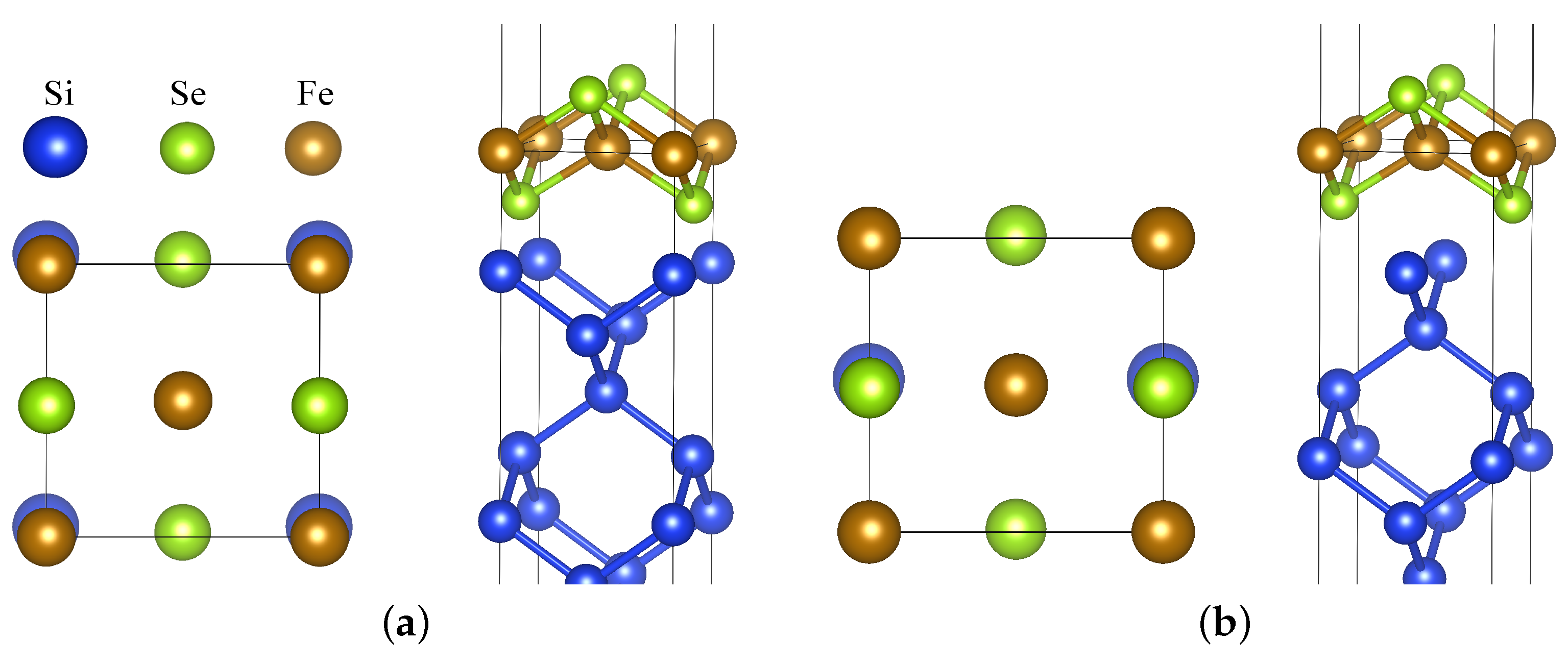
There are two plausible relative arrangements of the Si surface with regards to the FeSe ML, denoted as interface configurations IC1 and IC2 (see Figure 1). For IC1, interfacial Se are placed at sites where the next Si would be present if its lattice was continued. Within IC2, Se is placed similarly to if there was another FeSe layer with neighboring Se atoms located where topmost Si atoms are. IC1 is energetically more favorable for both NM and AFM cases according to our calculations. IC1 introduces a larger difference in the environment of the two Fe atom sublattices, possibly resulting in a difference between the corresponding magnetic moments. Notably, a similar situation occurs if a TixO2 interlayer is formed between SrTiO3 and FeSe [28].
For AFM FeSe, the spin moment on Fe is 2.09 μB in the case of stand-alone ML. When brought into contact with Si, the moments on the two Fe sublattices become slightly different: for IC1, these are 2.01 and 2.13 μB; for IC2, the difference from 2.09 μB is less than 0.01 μB. Note that FM bulk FeSe DFT calculations converge to an spin-unpolarized state (at each atom) even though the initial Fe potential was spin-polarized. One of the key parameters affecting the electronic structure of FeSe adlayers is the distance from the substrate. The optimal distance differs between the studied cases; it is always larger for AFM compared to NM cases and IC2 compared to IC1 configurations. In all cases, the distance was smaller than the value found for the SrTiO3 interface [16], probably due to the low atomic density of the Si lattice and the tendency of Si to form covalent bonds. For NM IC1, we obtain the shortest interplane distance , which is slightly larger than the chalcogen plane distance from the Fe plane. This corresponds to the distance between the nearest Si and Se atoms, which is close to the typical bond length between these atoms in SiSe systems [31].
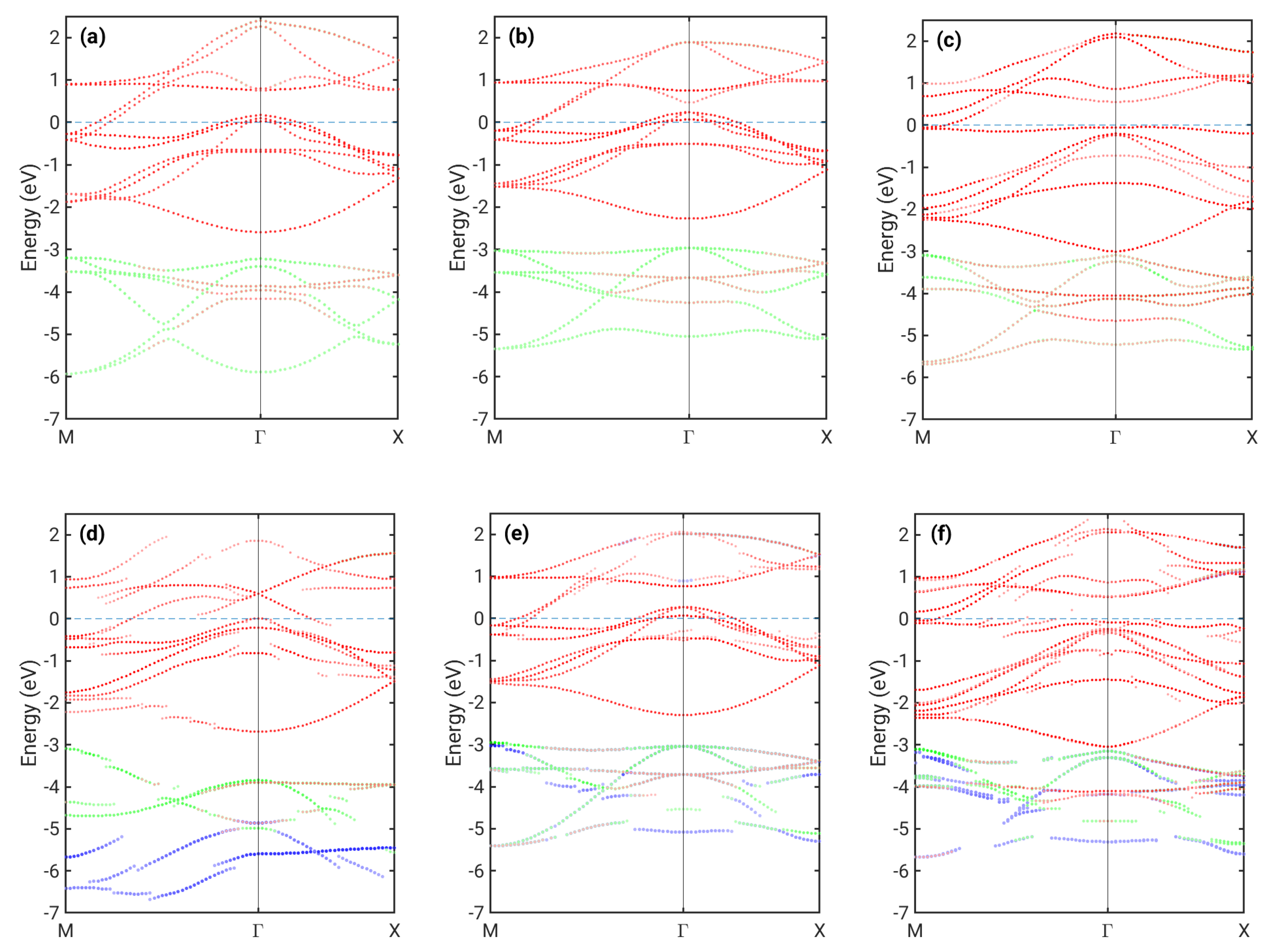
Let us first review the difference between the calculated in-plane band structure for NM monolayer FeSe and bulk FeSe (Figure 2a,b). In both cases, similar hole pockets near Γ and electron pockets near M are present with only quantitative differences between them, which is in approximate agreement with previous calculations [32]. The picture changes significantly for checkerboard AFM ordering (Figure 2c). Here, a pronounced flat band just below the Fermi level appears, and the hole pocket at Γ shifts below the Fermi level, as already shown for a 1 ML FeSe stand-alone structure [14].
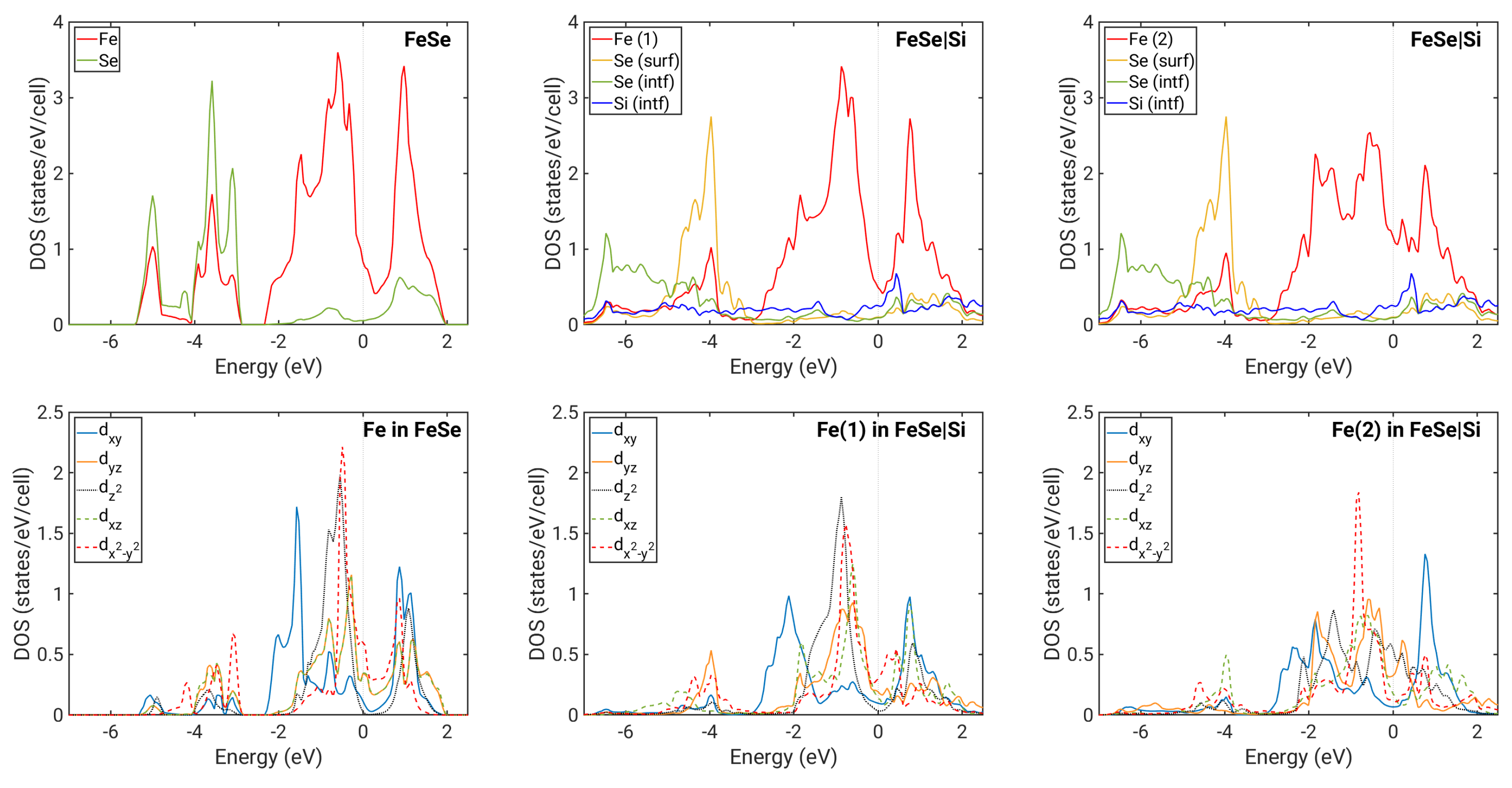
For FeSe on Si (Figure 2d–f), we see a more complex situation. There are effects due to hybridization with Si interfacial bands indicated by the loss of Fe/Se character at some points of the Brillouin zone. When this character is further reduced, the band becomes predominatly Si-type. Si bands are not shown in Figure 2; hence, such a band appears to be discontinuous. Hybridization significantly affects most Se bands. The flat band present in the AFM case just below the Fermi level (Figure 2f) is clearly also highly volatile to any interaction and strongly hybridized to Si bands. Furthermore, contributions from Se atoms in the plane closer to the surface and at the interface became unequal, with the latter occupying predominantly states further below the Fermi level, as is seen more clearly in their DOS (Figure 3).
In the case of the energetically most favorable NM IC1 configuration, the hybridization is stronger due to the smaller distance between FeSe and the substrate. In particular, the Fe band located below eV with an energy minimum at Γ is affected (Figure 2d). Fe in the position above Si atoms within the interface plane in the IC1 configuration (denoted Fe(2)) clearly has a significantly shorter distance to these Si atoms than the Fe(1) located on the other Fe sublattice (Figure 1). Therefore, Fe(2) is affected more by the interaction with Si. Figure 3 shows that the Fe(2) contribution to the DOS differs from that of the free-standing Fe DOS, while Fe(1) is much less modifed. Interfacial Se bands are now significantly broadened, and they provide a large contribution to DOS in energies even below eV, while DOS for the free-standing ML vanishes below ca. eV. Furthermore, the DOS at the Fermi level is overall increased for Fe(2).
The Fermi level for the case of the NM IC1 configuration is positioned differently in terms of the bands corresponding to the former hole and electron pockets. By comparing Figure 2b,d, we observe that some bands originally crossing the Fermi level are pushed below it, with only a small hole pocket at Γ remaining. However, our calculations do not show a significant charge transfer between Si and FeSe. In order to understand the shift of the Fermi level relative to different bands, we have also extracted the orbital-resolved DOS for Fe atoms, shown in Figure 3. We first note that for FeSe on Si, the degeneracy between and orbitals is lifted due to the reduced symmetry in the system. Interestingly, this loss of degeneracy has also been observed in bulk FeSe as a consequence of the nematic order [33,34]. The occupations of different orbitals change significantly between the free-standing 1ML NM case and the case of FeSe on Si (IC1). In particular, the occupation of is increased, while that of and is reduced (Table 1). This seems to be connected to the fact that the two FeSe electron pockets located at the M point become flatter when in the IC1 configuration. Furthermore, the outer one of them (mostly of character) is strongly hybridized with Si. The charge from these bands is transferred to hole pockets near Γ, which become almost fully occupied. The small peak in the interfacial Si DOS near eV indicates hybridization with Fe states. At approximately the same energy, a peak in the contribution to Fe(2) DOS is present without a counterpart in the free-standing ML. The strong coupling between Fe(2) and Si thus appears to be facilitated predominantly by states, which are extended spatially in the direction of the Fe(2)–Si bond.
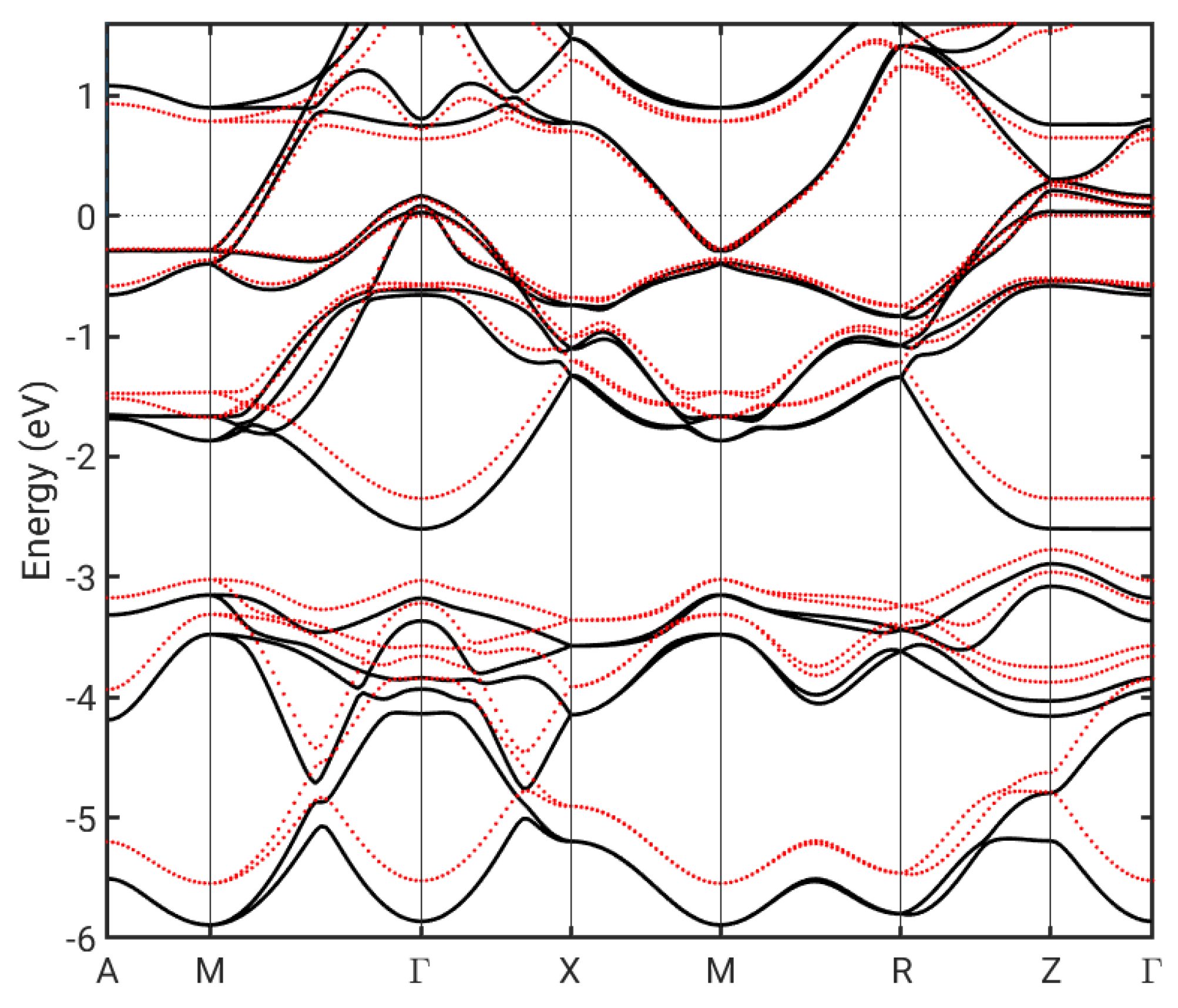
Some of the observed differences between the FeSe adlayer on Si and the FeSe bulk solution could originate from the Si-induced straining of the FeSe lattice. Strain has been shown to have an important effect on SC in the case of FeSe on SrTiO3 [35], where it leads to an increased Fe-Fe AFM coupling [36]. We have thus examined the effect of Si-induced strain on the bulk band structure, as shown in Figure 4. While some of the bands become less dispersive, the effect in the critical region near the Fermi level does not seem significant.
4. Discussion
High SC in FeSe monolayers has been associated to the absence of hole pockets around Γ. Hole-like bands were in that case observed slightly below the Fermi level. The so-called incipient bands located up to 100 meV below the Fermi level at Γ may participate in spin fluctuations predicted to lead to a high [37]. In our calculations, two of the hole-like FS sheets around Γ present in bulk FeSe are removed under the influence of the Si(001) interface, with only one small hole pocket remaining (Figure 2d). Just a slight electron doping would be needed to shift this hole pocket entirely under the Fermi level, which would lead to a bandstructure potentially consistent with the incipient band scenario. Such doping has been successfully facilitated experimentally by potassium deposition onto FeSe in the case of the SrTiO3 interface [8]. In reality, one should also take into account the fact that the result could be affected by Se vacancies, whose role has been found to be highly non-trivial for FeSe on SrTiO3 [38].
Our calculations assume a perfect interface between Si and FeSe. This condition may not be necessarily valid for real samples, e.g., due to surface reconstruction effects or intermixing between constituents. However, significant surface reconstructions, e.g., 2 × 1 on Si(001) surface, appear to be improbable. In experiments, interface quality can be partially controlled by various parameters during deposition processes, increasing the proportion of the perfect interface area in real samples. Dynamic stability studies using state-of-the-art DFT methods could help to resolve this problem, but that would go beyond the scope of this work and deserves a dedicated study. Note that FeSe/SrTiO3 interfaces had been found to be rather stable, which led to a suggestion of a superlattice based on repetitions of this interface [39].
We stress here that our theoretical contribution on FeSe–Si(001) interfaces is not only interesting from a fundamental physics point of view but may have an impact on future nanotechnological applications or in the area of quantum computing [40]. The Si(100) surface is the most important facet for silicon-based metal–oxide semiconductor device fabrication [41]. Moreover, we want to mention that instead of serving as a substrate, silicon may also become important to terminate and protect FeSe-based heterostructures from deterioration in air: most studies on SC in FeSe/SrTiO3 heterostructures use scanning-tunneling spectroscopy and angle-resolved photoemission spectroscopy (ARPES) studies performed under ultra-high vacuum conditions, but FeSe is found to be susceptible to contaminants, such as water, reducing Tc drastically [42].
5. Conclusions
We have examined the electronic structure of FeSe on Si(001) for both the NM and checkerboard AFM cases and different interface configurations. For the energetically favorable interface configuration, some of bands originally crossing the Fermi level and forming hole pockets are pushed below it, and the remaining hole pocket around Γ is significantly suppressed. The complete removal of hole pockets from the Fermi surface, as observed for the SrTiO3 interface, appears to be possible. Bands corresponding to electron pockets centered at M are flattened, and one of them is strongly hybridized with Si. This is connected to a redistribution of charge between different Fe orbitals, during which the degeneracy between and orbitals is lost. Experimental investigations of the FeSe–Si interface and its critical temperature would allow to test recent intensively discussed theory approaches linked to the interfacial high-Tc superconductivity for an entirely different, non-oxide substrate system. The evaluation of their role could lead to a better understanding of this intriguing phenomenon.
Author Contributions
Writing—original draft, K.C.; writing—review and editing, K.C. and J.H.; investigation, K.C. and P.V.; project administration, K.C. and J.H.; supervision, K.C.; visualization, K.C. and P.V.; funding acquisition, J.H.; All authors have read and agreed to the published version of the manuscript.
Funding
This research was funded by the Czech Science Foundation (Grant No. 19-13659S).
Data Availability Statement
Data presented in this article are available on request from the corresponding author.
Acknowledgments
Part of the calculations were enabled by resources provided by the Ministry of Education, Youth and Sports of the Czech Republic through e-INFRA CZ (ID:90140).
Conflicts of Interest
The authors declare no conflict of interest.
Abbreviations
The following abbreviations are used in this manuscript:
| NM | non-magnetic |
| AFM | anti-ferromagnetic |
| 2D | two-dimensional |
| DFT | density functional theory |
| ML | monolayer |
| SC | superconductor |
| GGA | generalized gradient approximation |
| PBE | Perdew–Burke–Ernzerhof |
| DOS | density of states |
References
- Liu, X.; Zhao, L.; He, S.; He, J.; Liu, D.; Mou, D.; Shen, B.; Hu, Y.; Huang, J.; Zhou, X.J. Electronic structure and superconductivity of FeSe-related superconductors. J. Phys. Condens. Matter 2015, 27, 183201. [Google Scholar] [CrossRef] [PubMed] [Green Version]
- Hsu, F.C.; Luo, J.Y.; Yeh, K.W.; Chen, T.K.; Huang, T.W.; Wu, P.M.; Lee, Y.C.; Huang, Y.L.; Chu, Y.Y.; Yan, D.C.; et al. Superconductivity in the PbO-type structure -FeSe. Proc. Natl. Acad. Sci. USA 2008, 105, 14262–14264. [Google Scholar] [CrossRef] [PubMed] [Green Version]
- Ge, J.F.; Liu, Z.L.; Liu, C.; Gao, C.L.; Qian, D.; Xue, Q.K.; Liu, Y.; Jia, J.F. Superconductivity above 100 K in single-layer FeSe films on doped SrTiO3. Nat. Mater. 2014, 14, 285–289. [Google Scholar] [CrossRef] [PubMed]
- Kelly, J.; Barends, R.; Fowler, A.G.; Megrant, A.; Jeffrey, E.; White, T.C.; Sank, D.; Mutus, J.Y.; Campbell, B.; Chen, Y.; et al. State preservation by repetitive error detection in a superconducting quantum circuit. Nature 2015, 519, 66–69. [Google Scholar] [CrossRef] [Green Version]
- Arute, F.; Arya, K.; Babbush, R.; Bacon, D.; Bardin, J.C.; Barends, R.; Biswas, R.; Boixo, S.; Brandao, F.G.S.L.; Buell, D.A.; et al. Quantum supremacy using a programmable superconducting processor. Nature 2019, 574, 505–510. [Google Scholar] [CrossRef] [PubMed] [Green Version]
- Lyatti, M.; Wolff, M.A.; Gundareva, I.; Kruth, M.; Ferrari, S.; Dunin-Borkowski, R.E.; Schuck, C. Energy-level quantization and single-photon control of phase slips in YBa2Cu3O7–x nanowires. Nat. Commun. 2020, 11, 763. [Google Scholar] [CrossRef] [Green Version]
- Hirschfeld, P.J.; Korshunov, M.M.; Mazin, I.I. Gap symmetry and structure of Fe-based superconductors. Rep. Prog. Phys. 2011, 74, 124508. [Google Scholar] [CrossRef] [Green Version]
- Miyata, Y.; Nakayama, K.; Sugawara, K.; Sato, T.; Takahashi, T. High-temperature superconductivity in potassium-coated multilayer FeSe thin films. Nat. Mater. 2015, 14, 775–779. [Google Scholar] [CrossRef]
- Shi, X.; Han, Z.Q.; Peng, X.L.; Richard, P.; Qian, T.; Wu, X.X.; Qiu, M.W.; Wang, S.C.; Hu, J.P.; Sun, Y.J.; et al. Enhanced superconductivity accompanying a Lifshitz transition in electron-doped FeSe monolayer. Nat. Commun. 2017, 8, 14988. [Google Scholar] [CrossRef] [Green Version]
- Kordyuk, A.A. Iron-based superconductors: Magnetism, superconductivity, and electronic structure (Review Article). Low Temp. Phys. 2012, 38, 888–899. [Google Scholar] [CrossRef] [Green Version]
- Coldea, A.I.; Watson, M.D. The Key Ingredients of the Electronic Structure of FeSe. Annu. Rev. Condens. Matter Phys. 2018, 9, 125–146. [Google Scholar] [CrossRef] [Green Version]
- Liu, K.; Lu, Z.Y.; Xiang, T. Atomic and electronic structures of FeSe monolayer and bilayer thin films on SrTiO3(001): First-principles study. Phys. Rev. B 2012, 85, 235123. [Google Scholar] [CrossRef] [Green Version]
- Ma, F.; Ji, W.; Hu, J.; Lu, Z.Y.; Xiang, T. First-Principles Calculations of the Electronic Structure of Tetragonal α-FeTe and α-FeSe Crystals: Evidence for a Bicollinear Antiferromagnetic Order. Phys. Rev. Lett. 2009, 102, 177003. [Google Scholar] [CrossRef] [PubMed] [Green Version]
- Bazhirov, T.; Cohen, M.L. Effects of charge doping and constrained magnetization on the electronic structure of an FeSe monolayer. J. Phys. Condens. Matter 2013, 25, 105506. [Google Scholar] [CrossRef] [PubMed]
- Zheng, F.; Wang, Z.; Kang, W.; Zhang, P. Antiferromagnetic FeSe monolayer on SrTiO3: The charge doping and electric field effects. Sci. Rep. 2013, 3, 2213. [Google Scholar] [CrossRef] [PubMed] [Green Version]
- Liu, K.; Zhang, B.J.; Lu, Z.Y. First-principles study of magnetic frustration in FeSe epitaxial films onSrTiO3. Phys. Rev. B 2015, 91, 045107. [Google Scholar] [CrossRef] [Green Version]
- Glasbrenner, J.K.; Mazin, I.I.; Jeschke, H.O.; Hirschfeld, P.J.; Fernandes, R.M.; Valentí, R. Effect of magnetic frustration on nematicity and superconductivity in iron chalcogenides. Nat. Phys. 2015, 11, 953–958. [Google Scholar] [CrossRef]
- Zhou, Y.; Miao, L.; Wang, P.; Zhu, F.; Jiang, W.; Jiang, S.; Zhang, Y.; Lei, B.; Chen, X.; Ding, H.; et al. Antiferromagnetic Order in Epitaxial FeSe Films on SrTiO3. Phys. Rev. Lett. 2018, 120, 097001. [Google Scholar] [CrossRef] [PubMed] [Green Version]
- Fikáček, J.; Procházka, P.; Stetsovych, V.; Průša, S.; Vondráček, M.; Kormoš, L.; Skála, T.; Vlaic, P.; Caha, O.; Carva, K.; et al. Step-edge assisted large scale FeSe monolayer growth on epitaxial Bi2Se3 thin films. New J. Phys. 2020, 22, 073050. [Google Scholar] [CrossRef]
- Manna, S.; Kamlapure, A.; Cornils, L.; Hänke, T.; Hedegaard, E.M.J.; Bremholm, M.; Iversen, B.B.; Hofmann, P.; Wiebe, J.; Wiesendanger, R. Interfacial superconductivity in a bi-collinear antiferromagnetically ordered FeTe monolayer on a topological insulator. Nat. Commun. 2017, 8, 14074. [Google Scholar] [CrossRef] [Green Version]
- The ELK Code. Available online: http://elk.sourceforge.net/ (accessed on 1 December 2021).
- Perdew, J.P.; Burke, K.; Ernzerhof, M. Generalized Gradient Approximation Made Simple. Phys. Rev. Lett. 1996, 77, 3865–3868. [Google Scholar] [CrossRef] [Green Version]
- Fernandes, R.M.; Vafek, O. Distinguishing spin-orbit coupling and nematic order in the electronic spectrum of iron-based superconductors. Phys. Rev. B 2014, 90, 214514. [Google Scholar] [CrossRef] [Green Version]
- Borisenko, S.V.; Evtushinsky, D.V.; Liu, Z.H.; Morozov, I.; Kappenberger, R.; Wurmehl, S.; Büchner, B.; Yaresko, A.N.; Kim, T.K.; Hoesch, M.; et al. Direct observation of spin–orbit coupling in iron-based superconductors. Nat. Phys. 2015, 12, 311–317. [Google Scholar] [CrossRef]
- dos Santos, R.B.; Rivelino, R.; Gueorguiev, G.K.; Kakanakova-Georgieva, A. Exploring 2D structures of indium oxide of different stoichiometry. CrystEngComm 2021, 23, 6661–6667. [Google Scholar] [CrossRef]
- Freitas, R.R.Q.; de Brito Mota, F.; Rivelino, R.; de Castilho, C.M.C.; Kakanakova-Georgieva, A.; Gueorguiev, G.K. Tuning band inversion symmetry of buckled III-Bi sheets by halogenation. Nanotechnology 2016, 27, 055704. [Google Scholar] [CrossRef] [PubMed]
- Haastrup, S.; Strange, M.; Pandey, M.; Deilmann, T.; Schmidt, P.S.; Hinsche, N.F.; Gjerding, M.N.; Torelli, D.; Larsen, P.M.; Riis-Jensen, A.C.; et al. The Computational 2D Materials Database: High-throughput modeling and discovery of atomically thin crystals. 2D Mater. 2018, 5, 042002. [Google Scholar] [CrossRef]
- Sims, H.; Leonard, D.N.; Birenbaum, A.Y.; Ge, Z.; Berlijn, T.; Li, L.; Cooper, V.R.; Chisholm, M.F.; Pantelides, S.T. Intrinsic interfacial van der Waals monolayers and their effect on the high-temperature superconductor FeSe/SrTiO3. Phys. Rev. B 2019, 100, 144103. [Google Scholar] [CrossRef] [Green Version]
- VESTA - Visualization for Electronic and STructural Analysis. Available online: https://jp-minerals.org/vesta (accessed on 3 December 2021).
- Momma, K.; Izumi, F. VESTA 3 for three-dimensional visualization of crystal, volumetric and morphology data. J. Appl. Crystallogr. 2011, 44, 1272–1276. [Google Scholar] [CrossRef]
- Jiang, H.; Zhao, T.; Ren, Y.; Zhang, R.; Wu, M. Ab initio prediction and characterization of phosphorene-like SiS and SiSe as anode materials for sodium-ion batteries. Sci. Bull. 2017, 62, 572–578. [Google Scholar] [CrossRef] [Green Version]
- Subedi, A.; Zhang, L.; Singh, D.J.; Du, M.H. Density functional study of FeS, FeSe, and FeTe: Electronic structure, magnetism, phonons, and superconductivity. Phys. Rev. B 2008, 78, 134514. [Google Scholar] [CrossRef] [Green Version]
- Nakayama, K.; Miyata, Y.; Phan, G.; Sato, T.; Tanabe, Y.; Urata, T.; Tanigaki, K.; Takahashi, T. Reconstruction of Band Structure Induced by Electronic Nematicity in an FeSe Superconductor. Phys. Rev. Lett. 2014, 113, 237001. [Google Scholar] [CrossRef] [Green Version]
- Watson, M.D.; Kim, T.K.; Haghighirad, A.A.; Davies, N.R.; McCollam, A.; Narayanan, A.; Blake, S.F.; Chen, Y.L.; Ghannadzadeh, S.; Schofield, A.J.; et al. Emergence of the nematic electronic state in FeSe. Phys. Rev. B 2015, 91, 155106. [Google Scholar] [CrossRef] [Green Version]
- Tan, S.; Zhang, Y.; Xia, M.; Ye, Z.; Chen, F.; Xie, X.; Peng, R.; Xu, D.; Fan, Q.; Xu, H.; et al. Interface-induced superconductivity and strain-dependent spin density waves in FeSe/SrTiO3 thin films. Nat. Mater. 2013, 12, 634–640. [Google Scholar] [CrossRef] [Green Version]
- Cao, H.Y.; Tan, S.; Xiang, H.; Feng, D.L.; Gong, X.G. Interfacial effects on the spin density wave in FeSe/SrTiO3 thin films. Phys. Rev. B 2014, 89, 014501. [Google Scholar] [CrossRef] [Green Version]
- Linscheid, A.; Maiti, S.; Wang, Y.; Johnston, S.; Hirschfeld, P. HighTcvia Spin Fluctuations from Incipient Bands: Application to Monolayers and Intercalates of FeSe. Phys. Rev. Lett. 2016, 117, 077003. [Google Scholar] [CrossRef] [Green Version]
- Berlijn, T.; Cheng, H.P.; Hirschfeld, P.J.; Ku, W. Doping effects of Se vacancies in monolayer FeSe. Phys. Rev. B 2014, 89, 020501. [Google Scholar] [CrossRef] [Green Version]
- Coh, S.; Lee, D.H.; Louie, S.G.; Cohen, M.L. Proposal for a bulk material based on a monolayer FeSe onSrTiO3 high-temperature superconductor. Phys. Rev. B 2016, 93, 245138. [Google Scholar] [CrossRef] [Green Version]
- Castelvecchi, D. Quantum computers ready to leap out of the lab in 2017. Nature 2017, 541, 9–10. [Google Scholar] [CrossRef] [PubMed]
- Yuan, S.; Wang, X.; Zhang, H.; Yuan, S. Reactive Molecular Dynamics on the Oxidation of H–Si(100) Surface: Effect of Humidity and Temperature. J. Phys. Chem. C 2019, 124, 1932–1940. [Google Scholar] [CrossRef]
- Bozovic, I.; Ahn, C. A new frontier for superconductivity. Nat. Phys. 2014, 10, 892–895. [Google Scholar] [CrossRef]
Figure 1.
Atomic structure of an FeSe monolayer on the Si(001) surface with two possible interface configurations: (a) IC1 and (b) IC2. For both, the top and side views are shown. Top view includes Si atoms from the interfacial layer plus Fe and Se atoms. Blue atoms (without label) correspond to Si. Images were drawn using the 3D visualization program for structural models, VESTA [29,30].

Figure 2.
Bandstructure cuts of (a) bulk NM FeSe, (b) free–standing NM FeSe ML, (c) free–standing AFM FeSe ML, (d) 1ML NM FeSe on top of Si, IC1, (e) 1ML NM FeSe on top of Si, IC2, and (f) 1ML AFM FeSe on top of Si. Colors indicate the atomic character as follows: red (Fe), blue (Se in the plane closer to the surface), and green (Se in the plane closer to Si). The composition of colors due to mixed character at individual k-points leads to other color tones seen above, e.g., orange-like.

Figure 3.
Densities of states. Upper panels: atomic resolved DOSes; lower panels: contributions to DOSes from separate Fe d orbitals. Left column of panels: shown for free-standing 1ML NM FeSe. Middle column of panels: shown for 1ML NM FeSe on top of Si (IC1) with contributions from the Fe(1) sublattice. Right column of panels: shown for 1ML NM FeSe on top of Si (IC1) with contributions from the Fe(2) sublattice.

Figure 4.
Bulk FeSe bandstructure for the ground state lattice (black lines) and for the lattice stretched to match that of Si (red lines).
Figure 4.
Bulk FeSe bandstructure for the ground state lattice (black lines) and for the lattice stretched to match that of Si (red lines).


Table 1.
Occupations of individual Fe orbitals in the different studied NM systems.
| Fe in free-standing FeSe | |||||
| Fe(1) in FeSe on Si, IC1 | |||||
| Fe(2) in FeSe on Si, IC1 |
Publisher’s Note: MDPI stays neutral with regard to jurisdictional claims in published maps and institutional affiliations. |
© 2022 by the authors. Licensee MDPI, Basel, Switzerland. This article is an open access article distributed under the terms and conditions of the Creative Commons Attribution (CC BY) license (https://creativecommons.org/licenses/by/4.0/).
Share and Cite
MDPI and ACS Style
Carva, K.; Vlaic, P.; Honolka, J. Electronic Structure of Monolayer FeSe on Si(001) from First Principles. Nanomaterials 2022, 12, 270. https://0-doi-org.brum.beds.ac.uk/10.3390/nano12020270
AMA Style
Carva K, Vlaic P, Honolka J. Electronic Structure of Monolayer FeSe on Si(001) from First Principles. Nanomaterials. 2022; 12(2):270. https://0-doi-org.brum.beds.ac.uk/10.3390/nano12020270
Chicago/Turabian StyleCarva, Karel, Petru Vlaic, and Jan Honolka. 2022. "Electronic Structure of Monolayer FeSe on Si(001) from First Principles" Nanomaterials 12, no. 2: 270. https://0-doi-org.brum.beds.ac.uk/10.3390/nano12020270
Note that from the first issue of 2016, this journal uses article numbers instead of page numbers. See further details here.