
Enhanced NH3 Sensing Performance of Mo Cluster-MoS2 Nanocomposite Thin Films via the Sulfurization of Mo6 Cluster Iodides Precursor
 , , , , , , , , and
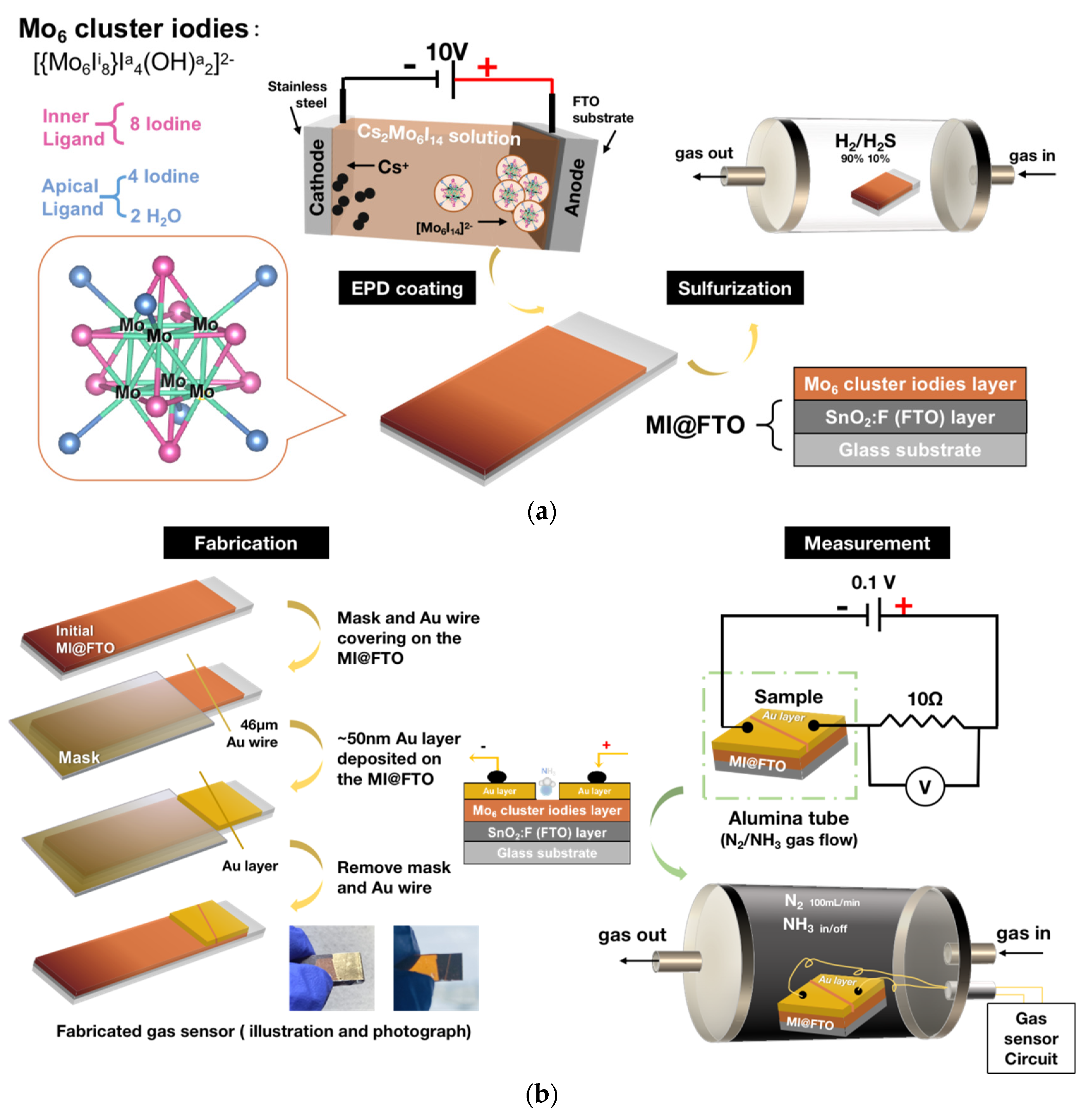
Abstract
:1. Introduction
2. Materials and Methods
2.1. Chemicals
2.2. Sulfurization Process
2.3. Fabrication and Measurement of Gas Sensor
2.4. Characterization
3. Results and Discussion
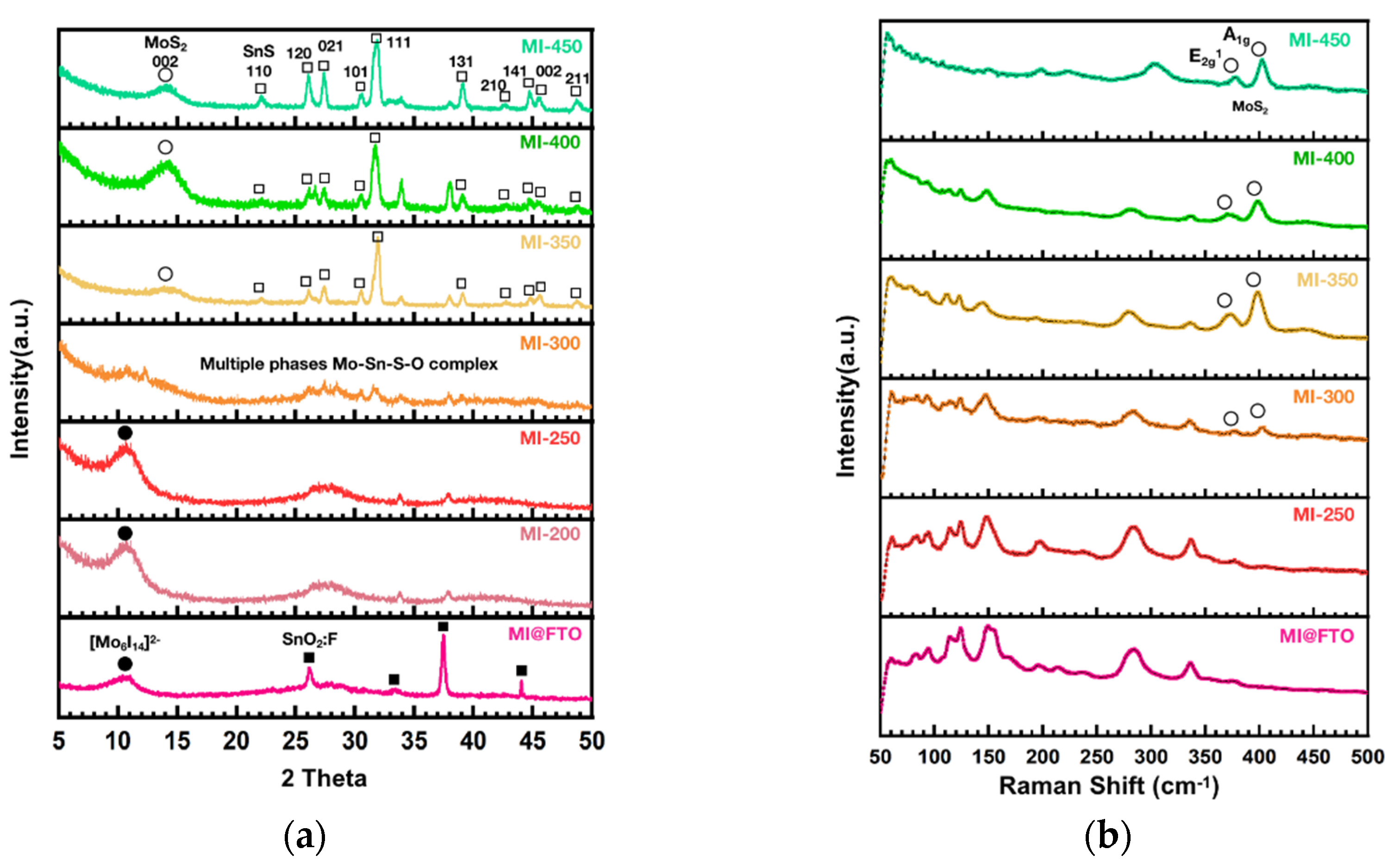
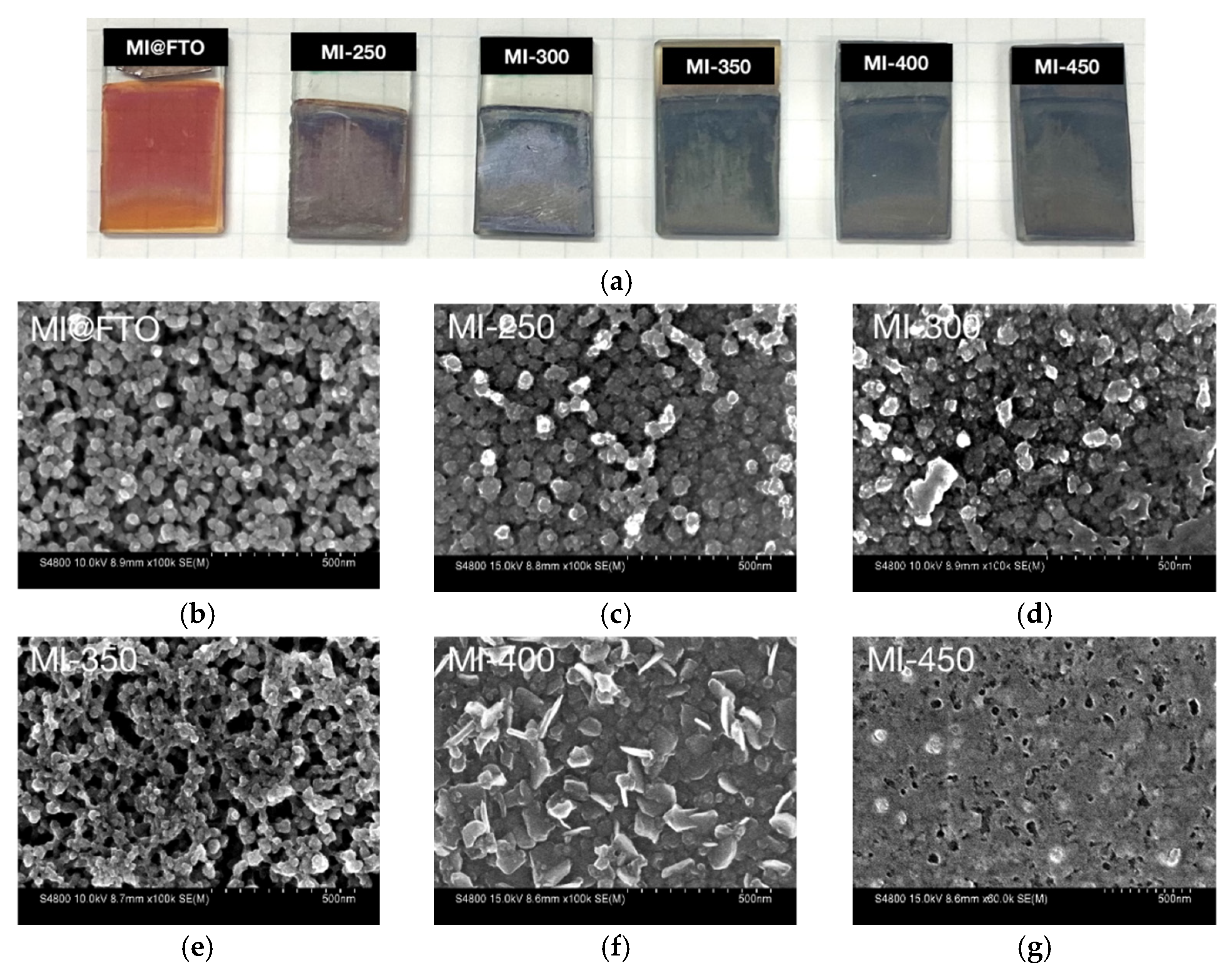
3.1. Structure and Morphology
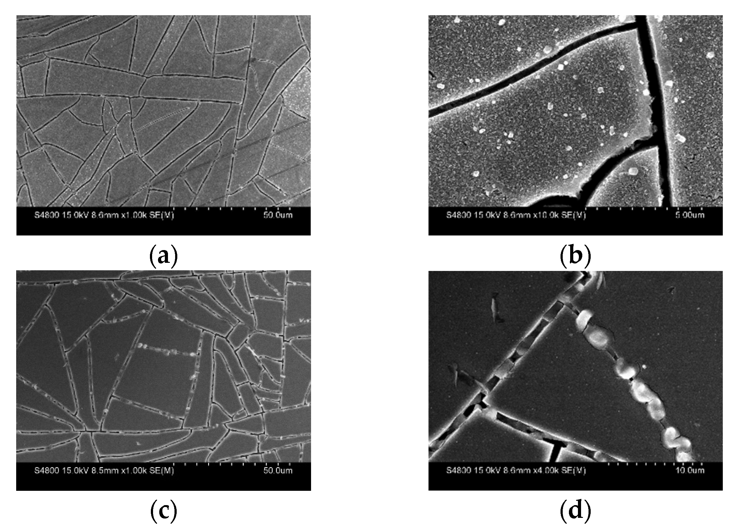
3.2. Mechanism of the MI@FTO Sulfurized into MoS2 and SnS crystal Growth Hypothesis
3.3. NH3 Sensor Application
4. Conclusions
Supplementary Materials
Author Contributions
Funding
Institutional Review Board Statement
Informed Consent Statement
Data Availability Statement
Acknowledgments
Conflicts of Interest
References
- Fiori, G.; Bonaccorso, F.; Iannaccone, G.; Palacios, T.; Neumaier, D.; Seabaugh, A.; Banerjee, S.K.; Colombo, L. Electronics Based on Two-Dimensional Materials. Nat. Nanotechnol. 2014, 9, 768–779. [Google Scholar] [CrossRef]
- Zeng, H.; Dai, J.; Yao, W.; Xiao, D.; Cui, X. Valley Polarization in MoS2 Monolayers by Optical Pumping. Nat. Nanotechnol. 2012, 7, 490–493. [Google Scholar] [CrossRef]
- Mak, K.F.; Lee, C.; Hone, J.; Shan, J.; Heinz, T.F. Atomically Thin MoS2: A New Direct-Gap Semiconductor. Phys. Rev. Lett. 2010, 105, 136805. [Google Scholar] [CrossRef] [Green Version]
- Chen, W.; Santos, E.J.G.; Zhu, W.; Kaxiras, E.; Zhang, Z. Tuning the Electronic and Chemical Properties of Monolayer MoS2 Adsorbed on Transition Metal Substrates. Nano Lett. 2013, 13, 509–514. [Google Scholar] [CrossRef]
- Chen, M.; Nam, H.; Wi, S.; Priessnitz, G.; Gunawan, I.M.; Liang, X. Multibit Data Storage States Formed in Plasma-Treated MoS2 Transistors. ACS Nano 2014, 8, 4023–4032. [Google Scholar] [CrossRef]
- Kang, J.; Liu, W.; Banerjee, K. High-Performance MoS2 Transistors with Low-Resistance Molybdenum Contacts. Appl. Phys. Lett. 2014, 104, 093106. [Google Scholar] [CrossRef] [Green Version]
- Tsai, M.-L.; Su, S.-H.; Chang, J.-K.; Tsai, D.-S.; Chen, C.-H.; Wu, C.-I.; Li, L.-J.; Chen, L.-J.; He, J.-H. Monolayer MoS2 Heterojunction Solar Cells. ACS Nano 2014, 8, 8317–8322. [Google Scholar] [CrossRef]
- Zhao, Y.; Ouyang, G. Thickness-Dependent Photoelectric Properties of MoS2/Si Heterostructure Solar Cells. Sci. Rep. 2019, 9, 17381. [Google Scholar] [CrossRef] [Green Version]
- Mao, J.; Wang, Y.; Zheng, Z.; Deng, D. The Rise of Two-Dimensional MoS2 for Catalysis. Front. Phys. 2018, 13, 138118. [Google Scholar] [CrossRef]
- Li, H.; Tsai, C.; Koh, A.L.; Cai, L.; Contryman, A.W.; Fragapane, A.H.; Zhao, J.; Han, H.S.; Manoharan, H.C.; Abild-Pedersen, F.; et al. Activating and Optimizing MoS2 Basal Planes for Hydrogen Evolution through the Formation of Strained Sulphur Vacancies. Nat. Mater. 2015, 15, 48–53. [Google Scholar] [CrossRef]
- Cao, Y. Roadmap and Direction toward High-Performance MoS2 Hydrogen Evolution Catalysts. ACS Nano 2021, 15, 11014–11039. [Google Scholar] [CrossRef]
- Akbari, E.; Jahanbin, K.; Afroozeh, A.; Yupapin, P.; Buntat, Z. Brief Review of Monolayer Molybdenum Disulfide Application in Gas Sensor. Phys. B Condens. Matter 2018, 545, 510–518. [Google Scholar] [CrossRef]
- Liu, B.; Chen, L.; Liu, G.; Abbas, A.N.; Fathi, M.; Zhou, C. High-Performance Chemical Sensing Using Schottky-Contacted Chemical Vapor Deposition Grown Monolayer MoS2 Transistors. ACS Nano 2014, 8, 5304–5314. [Google Scholar] [CrossRef]
- Donarelli, M.; Ottaviano, L. 2D Materials for Gas Sensing Applications: A Review on Graphene Oxide, MoS2, WS2 and Phosphorene. Sensors 2018, 18, 3638. [Google Scholar] [CrossRef] [Green Version]
- Kibsgaard, J.; Chen, Z.; Reinecke, B.N.; Jaramillo, T.F. Engineering the Surface Structure of MoS2 to Preferentially Expose Active Edge Sites for Electrocatalysis. Nat. Mater. 2012, 11, 963–969. [Google Scholar] [CrossRef]
- Li, X.; Li, T.; Ma, Y.; Wei, Q.; Qiu, W.; Guo, H.; Shi, X.; Zhang, P.; Asiri, A.M.; Chen, L.; et al. Boosted Electrocatalytic N2 Reduction to NH3 by Defect-Rich MoS2 Nanoflower. Adv. Energy Mater. 2018, 8, 1801357. [Google Scholar] [CrossRef]
- Le, D.; Rawal, T.B.; Rahman, T.S. Single-Layer MoS2 with Sulfur Vacancies: Structure and Catalytic Application. J. Phys. Chem. C 2014, 118, 5346–5351. [Google Scholar] [CrossRef]
- Li, L.; Qin, Z.; Ries, L.; Hong, S.; Michel, T.; Yang, J.; Salameh, C.; Bechelany, M.; Miele, P.; Kaplan, D.; et al. Role of Sulfur Vacancies and Undercoordinated Mo Regions in MoS2 Nanosheets toward the Evolution of Hydrogen. ACS Nano 2019, 13, 6824–6834. [Google Scholar] [CrossRef]
- Fei, H.; Guo, T.; Xin, Y.; Wang, L.; Liu, R.; Wang, D.; Liu, F.; Wu, Z. Sulfur Vacancy Engineering of MoS2 via Phosphorus Incorporation for Improved Electrocatalytic N2 Reduction to NH3. Appl. Catal. B Environ. 2022, 300, 120733. [Google Scholar] [CrossRef]
- Benck, J.D.; Hellstern, T.R.; Kibsgaard, J.; Chakthranont, P.; Jaramillo, T.F. Catalyzing the Hydrogen Evolution Reaction (HER) with Molybdenum Sulfide Nanomaterials. ACS Catal. 2014, 4, 3957–3971. [Google Scholar] [CrossRef]
- Tsai, C.; Li, H.; Park, S.; Park, J.; Han, H.S.; Nørskov, J.K.; Zheng, X.; Abild-Pedersen, F. Electrochemical Generation of Sulfur Vacancies in the Basal Plane of MoS2 for Hydrogen Evolution. Nat. Commun. 2017, 8, 15113. [Google Scholar] [CrossRef] [Green Version]
- Kumar, R.; Zheng, W.; Liu, X.; Zhang, J.; Kumar, M. MoS2-Based Nanomaterials for Room-Temperature Gas Sensors. Adv. Mater. Technol. 2020, 5, 1901062. [Google Scholar] [CrossRef]
- Ramanathan, A.A. Defect Functionalization of MoS2 Nanostructures as Toxic Gas Sensors: A Review. IOP Conf. Ser. Mater. Sci. Eng. 2018, 305, 012001. [Google Scholar] [CrossRef] [Green Version]
- Burman, D.; Ghosh, R.; Santra, S.; Ray, S.K.; Guha, P.K. Role of Vacancy Sites and UV-Ozone Treatment on Few Layered MoS2 nanoflakes for Toxic Gas Detection. Nanotechnology 2017, 28, 435502. [Google Scholar] [CrossRef]
- Xie, J.; Zhang, H.; Li, S.; Wang, R.; Sun, X.; Zhou, M.; Zhou, J.; Lou, X.W.D.; Xie, Y. Defect-Rich MoS2 Ultrathin Nanosheets with Additional Active Edge Sites for Enhanced Electrocatalytic Hydrogen Evolution. Adv. Mater. 2013, 25, 5807–5813. [Google Scholar] [CrossRef]
- Zhang, Z.; Dong, Y.; Sun, H.; Liu, G.; Liu, S.; Yang, X. Defect-Rich 2D Reticulated MoS2 Monolayers: Facile Hydrothermal Preparation and Marvellous Photoelectric Properties. J. Taiwan Inst. Chem. Eng. 2019, 101, 221–230. [Google Scholar] [CrossRef]
- Syari’ati, A.; Kumar, S.; Zahid, A.; El Yumin, A.A.; Ye, J.; Rudolf, P. Photoemission Spectroscopy Study of Structural Defects in Molybdenum Disulfide (MoS2) Grown by Chemical Vapor Deposition (CVD). Chem. Commun. 2019, 55, 10384–10387. [Google Scholar] [CrossRef] [Green Version]
- Young, B.T.; Pathan, M.A.K.; Jiang, T.; Le, D.; Marrow, N.; Nguyen, T.; Jordan, C.E.; Rahman, T.S.; Popolan-Vaida, D.M.; Vaida, M.E. Catalytic C2H2 Synthesis via Low Temperature CO Hydrogenation on Defect-Rich 2D-MoS2 and 2D-MoS2 Decorated with Mo Clusters. J. Chem. Phys. 2020, 152, 074706. [Google Scholar] [CrossRef]
- Zhang, Z.; Xu, X. Mechanistic Study on Enhanced Electrocatalytic Nitrogen Reduction Reaction by Mo Single Clusters Supported on MoS2. ACS Appl. Mater. Interfaces 2022, 14, 28900–28910. [Google Scholar] [CrossRef]
- Huang, W.; Wang, X.; Ji, X.; Zhang, Z.; Jin, C. In-Situ Fabrication of Mo6S6-Nanowire-Terminated Edges in Monolayer Molybdenum Disulfide. Nano Res. 2018, 11, 5849–5857. [Google Scholar] [CrossRef] [Green Version]
- Wang, X.-W.; Hou, L.-F.; Huang, W.; Ren, X.-B.; Ji, W.; Jin, C.-H. Mass Transport Induced Structural Evolution and Healing of Sulfur Vacancy Lines and Mo Chain in Monolayer MoS2. Rare Met. 2021, 41, 333–341. [Google Scholar] [CrossRef]
- Viršek, M.; Novak, N.; Filipič, C.; Kump, P.; Remškar, M.; Kutnjak, Z. Transport Properties in MoS2 Selective Morphology System. J. Appl. Phys. 2012, 112, 103710. [Google Scholar] [CrossRef]
- Viršek, M.; Krause, M.; Kolitsch, A.; Mrzel, A.; Iskra, I.; Škapin, S.D.; Remškar, M. The Transformation Pathways of Mo6S2I8 Nanowires into Morphology-Selective MoS2 Nanostructures. J. Phys. Chem. C 2010, 114, 6458–6463. [Google Scholar] [CrossRef]
- Chevrel, R.; Sergent, M.; Prigent, J. Sur de Nouvelles Phases Sulfurées Ternaires Du Molybdène. J. Solid State Chem. 1971, 3, 515–519. [Google Scholar] [CrossRef]
- Perrin, A.; Perrin, C. The Molybdenum and Rhenium Octahedral Cluster Chalcohalides in Solid State Chemistry: From Condensed to Discrete Cluster Units. Comptes Rendus Chim. 2012, 15, 815–836. [Google Scholar] [CrossRef]
- Fedorov, V. Metal Clusters. As They Were Born in Siberia. J. Clust. Sci. 2014, 26, 3–15. [Google Scholar] [CrossRef]
- Vorotnikova, N.A.; Vorotnikov, Y.A.; Novozhilov, I.N.; Syrokvashin, M.M.; Nadolinny, V.A.; Kuratieva, N.V.; Benoit, D.M.; Mironov, Y.V.; Walton, R.I.; Clarkson, G.J.; et al. 23-Electron Octahedral Molybdenum Cluster Complex [{Mo6I8}Cl6]−. Inorg. Chem. 2017, 57, 811–820. [Google Scholar] [CrossRef] [Green Version]
- Nguyen, N.T.K.; Lebastard, C.; Wilmet, M.; Dumait, N.; Renaud, A.; Cordier, S.; Ohashi, N.; Uchikoshi, T.; Grasset, F. A Review on Functional Nanoarchitectonics Nanocomposites Based on Octahedral Metal Atom Clusters (Nb6, Mo6, Ta6, W6, Re6): Inorganic 0D and 2D Powders and Films. Sci. Technol. Adv. Mater. 2022, 23, 547–578. [Google Scholar] [CrossRef]
- Costuas, K.; Garreau, A.; Bulou, A.; Fontaine, B.; Cuny, J.; Gautier, R.; Mortier, M.; Molard, Y.; Duvail, J.-L.; Faulques, E.; et al. Combined Theoretical and Time-Resolved Photoluminescence Investigations of [Mo6Bri8Bra6]2− Metal Cluster Units: Evidence of Dual Emission. Phys. Chem. Chem. Phys. 2015, 17, 28574–28585. [Google Scholar] [CrossRef]
- Sokolov, M.N.; Mihailov, M.A.; Peresypkina, E.V.; Brylev, K.A.; Kitamura, N.; Fedin, V.P. Highly Luminescent Complexes [Mo6X8(N-C3F7COO)6]2− (X = Br, I). Dalton Trans. 2011, 40, 6375. [Google Scholar] [CrossRef]
- Dierre, B.; Costuas, K.; Dumait, N.; Paofai, S.; Amela-Cortes, M.; Molard, Y.; Grasset, F.; Cho, Y.; Takahashi, K.; Ohashi, N.; et al. Mo6 Cluster-Based Compounds for Energy Conversion Applications: Comparative Study of Photoluminescence and Cathodoluminescence. Sci. Technol. Adv. Mater. 2017, 18, 458–466. [Google Scholar] [CrossRef] [PubMed] [Green Version]
- Dybtsev, D.; Serre, C.; Schmitz, B.; Panella, B.; Hirscher, M.; Latroche, M.; Llewellyn, P.L.; Cordier, S.; Molard, Y.; Haouas, M.; et al. Influence of [Mo6Br8F6]2− Cluster Unit Inclusion within the Mesoporous Solid MIL-101 on Hydrogen Storage Performance. Langmuir 2010, 26, 11283–11290. [Google Scholar] [CrossRef] [PubMed]
- Barras, A.; Das, M.R.; Devarapalli, R.R.; Shelke, M.V.; Cordier, S.; Szunerits, S.; Boukherroub, R. One-Pot Synthesis of Gold Nanoparticle/Molybdenum Cluster/Graphene Oxide Nanocomposite and Its Photocatalytic Activity. Appl. Catal. B Environ. 2013, 130–131, 270–276. [Google Scholar] [CrossRef]
- Nguyen, N.T.K.; Renaud, A.; Dierre, B.; Bouteille, B.; Wilmet, M.; Dubernet, M.; Ohashi, N.; Grasset, F.; Uchikoshi, T. Extended Study on Electrophoretic Deposition Process of Inorganic Octahedral Metal Clusters: Advanced Multifunctional Transparent Nanocomposite Thin Films. Bull. Chem. Soc. Jpn. 2018, 91, 1763–1774. [Google Scholar] [CrossRef] [Green Version]
- Renaud, A.; Jouan, P.-Y.; Dumait, N.; Ababou-Girard, S.; Barreau, N.; Uchikoshi, T.; Grasset, F.; Jobic, S.; Cordier, S. Evidence of the Ambipolar Behavior of Mo6 Cluster Iodides in All-Inorganic Solar Cells: A New Example of Nanoarchitectonic Concept. ACS Appl. Mater. Interfaces 2021, 14, 1347–1354. [Google Scholar] [CrossRef] [PubMed]
- Guy, K.; Tessier, F.; Kaper, H.; Grasset, F.; Dumait, N.; Demange, V.; Nishio, M.; Matsushita, Y.; Matsui, Y.; Takei, T.; et al. Original Synthesis of Molybdenum Nitrides Using Metal Cluster Compounds as Precursors: Applications in Heterogeneous Catalysis. Chem. Mater. 2020, 32, 6026–6034. [Google Scholar] [CrossRef]
- Zhang, M.Q.; Grasset, F.; Dumait, N.; Cordier, S.; Shimada, T.; Uchikoshi, T. Effect of Sulfurization Process on Octahedral Molybdenum Cluster from Mo6 Cluster to MoS2 Nanosheet. Key Eng. Mater. 2021, 904, 334–338. [Google Scholar] [CrossRef]
- Saito, G.; Hosoda, H.; Yoshida, Y.; Hagiwara, J.; Nishimura, K.; Yamochi, H.; Otsuka, A.; Hiramatsu, T.; Shimazaki, Y.; Kirakci, K.; et al. Synthesis and Properties of Charge-Transfer Solids with Cluster Units [Mo6X14]2− (X = Br, I). J. Mater. Chem. 2012, 22, 19774. [Google Scholar] [CrossRef]
- Kirakci, K.; Cordier, S.; Perrin, C. Synthesis and Characterization of Cs2Mo6X14 (X = Br or I) Hexamolybdenum Cluster Halides: Efficient Mo6 Cluster Precursors for Solution Chemistry Syntheses. Z. Anorg. Und Allg. Chem. 2005, 631, 411–416. [Google Scholar] [CrossRef]
- Nguyen, T.K.N.; Grasset, F.; Dierre, B.; Matsunaga, C.; Cordier, S.; Lemoine, P.; Ohashi, N.; Uchikoshi, T. Fabrication of Transparent Thin Film of Octahedral Molybdenum Metal Clusters by Electrophoretic Deposition. ECS J. Solid State Sci. Technol. 2016, 5, R178–R186. [Google Scholar] [CrossRef]
- Renaud, A.; Nguyen, T.K.N.; Grasset, F.; Raissi, M.; Guillon, V.; Delabrouille, F.; Dumait, N.; Jouan, P.-Y.; Cario, L.; Jobic, S.; et al. Preparation by Electrophoretic Deposition of Molybdenum Iodide Cluster-Based Functional Nanostructured Photoelectrodes for Solar Cells. Electrochim. Acta 2019, 317, 737–745. [Google Scholar] [CrossRef]
- Akram, H.; Mateos-Pedrero, C.; Gallegos-Suarez, E.; Chafik, T.; Guerrero-Ruiz, A.; Rodríguez-Ramos, I. Effect of Surfactant Concentration on the Morphology of MoxSy Nanoparticles Prepared by a Solvothermal Route. Green Process. Synth. 2017, 6, 161–171. [Google Scholar] [CrossRef] [Green Version]
- Polivtseva, S.; Acik, I.O.; Katerski, A.; Mere, A.; Mikli, V.; Krunks, M. Spray Pyrolysis Deposition of SnxSy Thin Films. Energy Procedia 2014, 60, 156–165. [Google Scholar] [CrossRef] [Green Version]
- Kaidi, Z.; Boulanger, C.; Lecuire, J.M.; Lemée, N.; Guilloux-Viry, M.; Perrin, A. Ternary Molybdenum Cluster Sulfides: Electrochemical and Chemical Behavior of in Situ Pulsed Laser Deposited Thin Films. Solid State Sci. 1999, 1, 623–635. [Google Scholar] [CrossRef]
- Genuit, D.; Bezverkhyy, I.; Afanasiev, P. Solution Preparation of the Amorphous Molybdenum Oxysulfide MoOS2 and Its Use for Catalysis. J. Solid State Chem. 2005, 178, 2759–2765. [Google Scholar] [CrossRef]
- Liu, G.; Li, Z.; Hasan, T.; Chen, X.; Zheng, W.; Feng, W.; Jia, D.; Zhou, Y.; Hu, P. Vertically Aligned Two-Dimensional SnS2 Nanosheets with a Strong Photon Capturing Capability for Efficient Photoelectrochemical Water Splitting. J. Mater. Chem. A 2017, 5, 1989–1995. [Google Scholar] [CrossRef] [Green Version]
- Burton, L.A.; Colombara, D.; Abellon, R.D.; Grozema, F.C.; Peter, L.M.; Savenije, T.J.; Dennler, G.; Walsh, A. Synthesis, Characterization, and Electronic Structure of Single-Crystal SnS, Sn2S3, and SnS2. Chem. Mater. 2013, 25, 4908–4916. [Google Scholar] [CrossRef]
- Harada, K.; Nguyen, T.K.N.; Grasset, F.; Comby-Zerbino, C.; MacAleese, L.; Chirot, F.; Dugourd, P.; Dumait, N.; Cordier, S.; Ohashi, N.; et al. Light-Dependent Ionic-Electronic Conduction in an Amorphous Octahedral Molybdenum Cluster Thin Film. NPG Asia Mater. 2022, 14, 21. [Google Scholar] [CrossRef]
- Chen, Z.; Cummins, D.; Reinecke, B.N.; Clark, E.; Sunkara, M.K.; Jaramillo, T.F. Core–Shell MoO3–MoS2 Nanowires for Hydrogen Evolution: A Functional Design for Electrocatalytic Materials. Nano Lett. 2011, 11, 4168–4175. [Google Scholar] [CrossRef]
- Saito, N.; Cordier, S.; Lemoine, P.; Ohsawa, T.; Wada, Y.; Grasset, F.; Cross, J.S.; Ohashi, N. Lattice and Valence Electronic Structures of Crystalline Octahedral Molybdenum Halide Clusters-Based Compounds, Cs2[Mo6X14] (X = Cl, Br, I), Studied by Density Functional Theory Calculations. Inorg. Chem. 2017, 56, 6234–6243. [Google Scholar] [CrossRef]
- Rodenes, M.; Gonell, F.; Martín, S.; Corma, A.; Sorribes, I. Molecularly Engineering Defective Basal Planes in Molybdenum Sulfide for the Direct Synthesis of Benzimidazoles by Reductive Coupling of Dinitroarenes with Aldehydes. JACS Au 2022, 2, 601–612. [Google Scholar] [CrossRef] [PubMed]
- Fominski, V.; Demin, M.; Nevolin, V.; Fominski, D.; Romanov, R.; Gritskevich, M.; Smirnov, N. Reactive Pulsed Laser Deposition of Clustered-Type MoSx (X ~ 2, 3, and 4) Films and Their Solid Lubricant Properties at Low Temperature. Nanomaterials 2020, 10, 653. [Google Scholar] [CrossRef] [PubMed] [Green Version]
- Lee, C.-H.; Lee, S.; Lee, Y.-K.; Jung, Y.C.; Ko, Y.-I.; Lee, D.C.; Joh, H.-I. Understanding the Origin of Formation and Active Sites for Thiomolybdate [Mo3S13]2– Clusters as Hydrogen Evolution Catalyst through the Selective Control of Sulfur Atoms. ACS Catal. 2018, 8, 5221–5227. [Google Scholar] [CrossRef]
- Seo, B.; Jung, G.Y.; Lee, S.J.; Baek, D.S.; Sa, Y.J.; Ban, H.W.; Son, J.S.; Park, K.; Kwak, S.K.; Joo, S.H. Monomeric MoS42–-Derived Polymeric Chains with Active Molecular Units for Efficient Hydrogen Evolution Reaction. ACS Catal. 2019, 10, 652–662. [Google Scholar] [CrossRef]
- Pritzi, M.; Pascher, T.F.; Grutza, M.-L.; Kurz, P.; Ončák, M.; Beyer, M.K. Decomposition of Halogenated Molybdenum Sulfide Dianions [Mo3S7X6]2– (X = Cl, Br, I). J. Am. Soc. Mass Spectrom. 2022, 33, 1753–1760. [Google Scholar] [CrossRef]
- de Jong, A.M.; Borg, H.J.; van IJzendoorn, L.J.; Soudant, V.G.F.M.; de Beer, V.H.J.; van Veen, J.A.R.; Niemantsverdriet, J.W. Sulfidation Mechanism by Molybdenum Catalysts Supported on Silica/Silicon(100) Model Support Studied by Surface Spectroscopy. J. Phys. Chem. 1993, 97, 6477–6483. [Google Scholar] [CrossRef] [Green Version]
- Ghosh, R.N.; Baker, G.L.; Ruud, C.; Nocera, D.G. Fiber-Optic Oxygen Sensor Using Molybdenum Chloride Cluster Luminescence. Appl. Phys. Lett. 1999, 75, 2885–2887. [Google Scholar] [CrossRef] [Green Version]
- Ghosh, R.N.; Askeland, P.A.; Kramer, S.; Loloee, R. Optical Dissolved Oxygen Sensor Utilizing Molybdenum Chloride Cluster Phosphorescence. Appl. Phys. Lett. 2011, 98, 221103. [Google Scholar] [CrossRef] [Green Version]
- Khazieva, A.; Kholin, K.; Nizameev, I.; Brylev, K.; Kashnik, I.; Voloshina, A.; Lyubina, A.; Gubaidullin, A.; Daminova, A.; Petrov, K.; et al. Surface Modification of Silica Nanoparticles by Hexarhenium Anionic Cluster Complexes for PH-Sensing and Staining of Cell Nuclei. J. Colloid Interface Sci. 2021, 594, 759–769. [Google Scholar] [CrossRef]
- Elistratova, J.; Mikhailov, M.; Burilov, V.; Babaev, V.; Rizvanov, I.; Mustafina, A.; Abramov, P.; Sokolov, M.; Konovalov, A.; Fedin, V. Supramolecular Assemblies of Triblock Copolymers with Hexanuclear Molybdenum Clusters for Sensing Antibiotics in Aqueous Solutions via Energy Transfer. RSC Adv. 2014, 4, 27922–27930. [Google Scholar] [CrossRef]
- Nguyen, T.K.N.; Dumait, N.; Grasset, F.; Cordier, S.; Berthebaud, D.; Matsui, Y.; Ohashi, N.; Uchikoshi, T. Zn–al Layered Double Hydroxide Film Functionalized by a Luminescent Octahedral Molybdenum Cluster: Ultraviolet–Visible Photoconductivity Response. ACS Appl. Mater. Interfaces 2020, 12, 40495–40509. [Google Scholar] [CrossRef] [PubMed]
- Cao, J.; Chen, Q.; Wang, X.; Zhang, Q.; Yu, H.-D.; Huang, X.; Huang, W. Recent Development of Gas Sensing Platforms Based on 2D Atomic Crystals. Research 2021, 2021, 9863038. [Google Scholar] [CrossRef] [PubMed]
- Late, D.J.; Huang, Y.-K.; Liu, B.; Acharya, J.; Shirodkar, S.N.; Luo, J.; Yan, A.; Charles, D.; Waghmare, U.V.; Dravid, V.P.; et al. Sensing Behavior of Atomically Thin-Layered MoS2 Transistors. ACS Nano 2013, 7, 4879–4891. [Google Scholar] [CrossRef] [PubMed]
- Wang, Y.; Duan, L.; Deng, Z.; Liao, J. Electrically Transduced Gas Sensors Based on Semiconducting Metal Oxide Nanowires. Sensors 2020, 20, 6781. [Google Scholar] [CrossRef]
- Shang, H.; Wang, T.; Zhang, W. Sulfur Vacancy Formation at Different MoS2 Edges during Hydrodesulfurization Process: A DFT Study. Chem. Eng. Sci. 2019, 195, 208–217. [Google Scholar] [CrossRef]
- Yang, L.; Majumdar, K.; Liu, H.; Du, Y.; Wu, H.; Hatzistergos, M.; Hung, P.Y.; Tieckelmann, R.; Tsai, W.; Hobbs, C.; et al. Chloride Molecular Doping Technique on 2D Materials: WS2 and MoS2. Nano Lett. 2014, 14, 6275–6280. [Google Scholar] [CrossRef] [Green Version]
- Murugan, P.; Kumar, V.; Kawazoe, Y.; Ota, N. Assembling Nanowires from Mo−S Clusters and Effects of Iodine Doping on Electronic Structure. Nano Lett. 2007, 7, 2214–2219. [Google Scholar] [CrossRef]
- Yuan, Z.; Liu, Y.; Zhang, J.; Meng, F.; Zhang, H. Rose-like MoO3/MoS2/RGO Low-Temperature Ammonia Sensors Based on Multigas Detection Methods. IEEE Trans. Instrum. Meas. 2021, 70, 1–9. [Google Scholar] [CrossRef]
- Kim, Y.; Lee, S.; Song, J.; Ko, K.Y.; Woo, W.J.; Lee, S.W.; Park, M.; Lee, H.; Lee, Z.; Choi, H.; et al. 2D Transition Metal Dichalcogenide Heterostructures for P- and N-Type Photovoltaic Self-Powered Gas Sensor. Adv. Funct. Mater. 2020, 30, 2003360. [Google Scholar] [CrossRef]
- Casanova-Chafer, J.; Garcia-Aboal, R.; Atienzar, P.; Feliz, M.; Llobet, E. Octahedral Molybdenum Iodide Clusters Supported on Graphene for Resistive and Optical Gas Sensing. ACS Appl. Mater. Interfaces 2022, 14, 57122–57132. [Google Scholar] [CrossRef]


Disclaimer/Publisher’s Note: The statements, opinions and data contained in all publications are solely those of the individual author(s) and contributor(s) and not of MDPI and/or the editor(s). MDPI and/or the editor(s) disclaim responsibility for any injury to people or property resulting from any ideas, methods, instructions or products referred to in the content. |
© 2023 by the authors. Licensee MDPI, Basel, Switzerland. This article is an open access article distributed under the terms and conditions of the Creative Commons Attribution (CC BY) license (https://creativecommons.org/licenses/by/4.0/).
Share and Cite
Zhang, M.; Grasset, F.; Masubuchi, Y.; Shimada, T.; Nguyen, T.K.N.; Dumait, N.; Renaud, A.; Cordier, S.; Berthebaud, D.; Halet, J.-F.; et al. Enhanced NH3 Sensing Performance of Mo Cluster-MoS2 Nanocomposite Thin Films via the Sulfurization of Mo6 Cluster Iodides Precursor. Nanomaterials 2023, 13, 478. https://0-doi-org.brum.beds.ac.uk/10.3390/nano13030478
Zhang M, Grasset F, Masubuchi Y, Shimada T, Nguyen TKN, Dumait N, Renaud A, Cordier S, Berthebaud D, Halet J-F, et al. Enhanced NH3 Sensing Performance of Mo Cluster-MoS2 Nanocomposite Thin Films via the Sulfurization of Mo6 Cluster Iodides Precursor. Nanomaterials. 2023; 13(3):478. https://0-doi-org.brum.beds.ac.uk/10.3390/nano13030478
Chicago/Turabian StyleZhang, Meiqi, Fabien Grasset, Yuji Masubuchi, Toshihiro Shimada, Thi Kim Ngan Nguyen, Noée Dumait, Adèle Renaud, Stéphane Cordier, David Berthebaud, Jean-François Halet, and et al. 2023. "Enhanced NH3 Sensing Performance of Mo Cluster-MoS2 Nanocomposite Thin Films via the Sulfurization of Mo6 Cluster Iodides Precursor" Nanomaterials 13, no. 3: 478. https://0-doi-org.brum.beds.ac.uk/10.3390/nano13030478