
Graphene Hybrid Metasurfaces for Mid-Infrared Molecular Sensors

1
Institute of Solid State Physics, University of Latvia, LV-1063 Riga, Latvia
2
RISE Research Institutes of Sweden AB, Box 1070, SE-164 25 Kista, Sweden
3
School of Information Technology, Halmstad University, SE-301 18 Halmstad, Sweden
*
Authors to whom correspondence should be addressed.
Nanomaterials 2023, 13(14), 2113; https://0-doi-org.brum.beds.ac.uk/10.3390/nano13142113
Submission received: 15 June 2023
/
Revised: 12 July 2023
/
Accepted: 18 July 2023
/
Published: 20 July 2023
(This article belongs to the Special Issue Graphene-Based Optoelectronic and Plasmonic Devices)
Abstract
:We integrated graphene with asymmetric metal metasurfaces and optimised the geometry dependent photoresponse towards optoelectronic molecular sensor devices. Through careful tuning and characterisation, combining finite-difference time-domain simulations, electron-beam lithography-based nanofabrication, and micro-Fourier transform infrared spectroscopy, we achieved precise control over the mid-infrared peak response wavelengths, transmittance, and reflectance. Our methods enabled simple, reproducible and targeted mid-infrared molecular sensing over a wide range of geometrical parameters. With ultimate minimization potential down to atomic thicknesses and a diverse range of complimentary nanomaterial combinations, we anticipate a high impact potential of these technologies for environmental monitoring, threat detection, and point of care diagnostics.
1. Introduction
Distinctive mid-infrared (MIR) molecular vibrations, ranging between ~2 and 12 μm, act as characteristic ‘molecular fingerprints’ for label-free identification of a wide range of chemicals and biomolecules. Usefully, atmospheric transparency windows, at 3–5 μm and 8–13 μm, enable a range of applications such as CO2 gas sensing and alcohol detection. Within the same MIR spectral range, black body radiation can also be utilised for photodetection and thermal imaging technologies. Taken together, MIR technologies have a substantial role in environmental monitoring, medical diagnosis, and security. However, in comparison to other wavelength regions, there exists a relative lack of MIR sources, detectors, and methodologies.
The current state-of-the-art technologies for MIR sensors are based on semiconductor bulk or quantum structures, such as gallium arsenide (GaAs), indium antimonide (InSb), and mercury-cadmium-telluride (MCT) [1]. Whilst these detectors offer very high sensitivity performance, their wider implementation and dissemination is significantly limited by a combination of high costs, limited spectral range, scarce materials, temperature sensitivity, and need for cooling. As a result, commercially available MIR sensing technologies are typically bulky and expensive, requiring specially controlled operating conditions. Whilst MIR technologies continue to develop, alternative materials and approaches are in high demand to meet the multiple challenges of device sensitivity, spectral range, size, cost, and power consumption [1,2,3].
A new family of low dimensional nanomaterials (graphene, transition metal dichalcogenides, topological insulators) offer unique optoelectronic functionalities and new technological solutions beyond those attainable with conventional semiconductors [4,5,6,7,8,9]. Graphene-based devices, in particular, attracted extensive research and attention due to their unique optoelectronic properties, broadband absorption, and electronic tuneability. For example, graphene shows good potential as atomically thin transparent conductive electrodes, combining high optical transparency (over 97%) for a wide range of wavelengths with high charge carrier mobilities for ultrafast devices [10,11]. Device performances can be extended down to very low charge carrier densities and are robust over a broad range of temperatures, allowing relatively relaxed operational requirements and conditions [12,13,14].
One practical limitation is the effect of charge inhomogeneity and scattering arising from the underlying substrate (typically SiO2, SiC, quartz) or from environmental and atmospheric dopants [15,16,17,18]. A range of technological solutions is being developed for surface control and stabilisation, such as encapsulation by polymers [19,20] or boron nitride layers [21,22]. In addition, improvements to the growth and transfer processes allow integration of graphene layers to a wide range of substrates and devices, with increasingly demonstrated and established CMOS compatibility [23,24]. For the optimisation of these optoelectronic devices, it is important to understand the material properties and performance, both individually and in combination, in the operational range of interest (wavelength, atmosphere, temperature). However, to date, the majority of literature reports focused on the visible to UV wavelengths, whilst the mid-infrared spectral region remained relatively underexplored.
A significant challenge for these nanoscale materials is to achieve sufficiently strong optical coupling, due in part to a size mismatch of several orders of magnitude with micrometre scale wavelengths. One promising approach to increase the photonic interaction with atomic materials, and molecules, is through nanoplasmonics [25,26]. Graphene is in itself capable of exhibiting plasmonic behaviour that can be enhanced and tuned by geometric patterning [27,28,29]. An alternate approach is to combine graphene with other plasmonic materials to form hybrid plasmonic structures, through near-field coupling [30,31,32,33]. Taking this approach one step further, the plasmonic nanoantenna can also be precision designed and patterned to form sub-wavelength arrays of quasi-2D metastructures or metasurfaces [34,35,36,37].
Metasurface technologies have a high complementarity and compatibility with 2D nanomaterials, with integration potential greater than the sum of their parts. One important benefit is precision photonic design of spectral selectivity, polarization, and focussing based primarily on lateral geometrical patterning where underlying fabrication methods are already well developed and CMOS compatible. Lateral geometric selectivity also allows for relatively straightforward multiplexing or pixelation of different devices, for enhanced selectivity, comparative analysis, and multi- or hyper-spectral detection and imaging. From the reverse perspective, functional 2D nanomaterials, such as graphene, offer additional functionalities such as dynamic tunability of the spectral photoresponse wavelength by electrostatic or electrochemical gating [38,39,40].
In recent years, there have been several significant reports exploring such MIR hybrid-graphene metasurfaces with potential for molecular sensing applications [32]. There can be considered three primary molecular sensing mechanisms for such systems: (i) optical sensing by photodetection, (ii) enhancement of the molecular absorption, (iii) peak wavelength shifts and modulation. For example, proof-of-principle photodetection devices were demonstrated by graphene-metal square micropatch arrays with MIR wavelength selective photoresponse [41,42] and ultrafast broadband photodetection by gold nanostripes with MIR photodetector responsivity up to ~2 A.W−1 at room temperature [43]. However, substantial challenges remain in the design, and a demonstration of these technologies to combine high photoresponsivity, precisely targeted wavelength selectivity, and implementation under application relevant operating conditions.
In this work, we demonstrated the design, fabrication, and characterization of hybrid-graphene metasurface devices towards geometrically tuneable molecular sensors for CO2 and alcohol detection. Electron beam lithography-based nanofabrication was combined with micro-Fourier transform infrared (μFTIR) spectroscopy to understand the key geometric tuning parameters for optimising MIR interaction and wavelength selectivity. The role of graphene for optoelectronic hybrid metasurface devices was confirmed and clarified by finite-difference time-domain (FDTD) studies. Moreover, the technological approaches described are readily scalable for industrial applications, where there is a high demand in a wide range of applications such as air quality inspection, automotive vehicle safety systems, alcohol sensing, healthcare, and security.
2. Materials and Methods
2.1. Metal Metasurface Fabrication
Asymmetric metal nanoantenna metasurface arrays were fabricated by electron beam lithography and optically characterised by micro-Fourier transform infrared spectroscopy. A SiO2 surface, thickness 192 nm, was thermally grown by standard PECVD on a commercially available double-side-polished silicon wafer, of thickness 525 μm (MicroChemicals, Ulm, Germany). The wafer was diced into chips of dimensions 10 × 10 or 20 × 20 mm2. The nanostructured arrays were then defined with a Raith eLine Plus electron beam lithography system (Raith, Dortmund, Germany) using polymethyl methacrylate (950PMMA A4 PMMA, Micro Resist Technology, Berlin, Germany) spin-coated at 4000 r.p.m. for 1 min, baked at 180 °C. Initial geometrical design parameters were determined with input from FDTD studies. The metal nanostructures were deposited in an Edwards Auto 306 thermal evaporator (Edwards, Burgess Hill, UK) (vacuum pressure 10−6 mBar), to cover large surface areas (2 × 2 to 10 × 10 mm2) of the SiO2 substrates. Following metal lift-off and solvent based cleaning (acetone, isopropanol), the surface geometries were analysed by scanning electron microscopy (SEM), using the same eLine system.
Dimensions of the metal surface arrays were determined with an approximate measurement uncertainty of 0.025 μm, originating from geometric non-uniformity of fabricated metal nanoantenna and SEM measurement precision. Both the array-to-array and wafer-to-wafer repeatability was found to be within this same uncertainty range. Deposited metal thicknesses were verified with a Dektak 150 Surface Profiler (Veeco, Santa Barbara, CA, USA) within 2 nm. Thicknesses of the deposited Au nanoantenna structures were 50 ± 5 nm.
2.2. Integration of Graphene with Metal Arrays to Form Hybrid Metasurfaces
Two approaches were implemented for integrating the metal metastructures with monolayer CVD graphene (Graphenea, San Sebastián, Spain): (1) graphene transfer onto pre-fabricated and characterised metal arrays and (2) direct metal deposition on the graphene surface. Transferring graphene allowed direct comparison of optically characterized surfaces and reduced risks related to graphene–metal adhesion. Nominally single layer graphene was acquired from and transferred on to the fabricated and optically characterised metal arrays on SiO2 substrates by an adhesive transfer method [24]. The presence of graphene layers was confirmed by a combination of contrast enhanced optical microscopy [44], electrical conductivity, and confocal micro-Raman analysis (S&I Spectroscopy & Imaging, Warstein, Germany).
Graphene optoelectronic device structures were patterned by electron beam lithography, graphene plasma ashing, metallisation, and lift-off as described in [45]. Material and device conductivity were measured at room temperature in an electronic probe station and 2450 SourceMeter (Keithley, Cleveland, OH, USA). In the absence of graphene, macroscopic surface conductivity was too low to measure for the Au metasurfaces on SiO2, with resistivities of a few Ω on the Au contacts, indicating correctly isolated Au nanostructures.
With the addition of graphene, two-dimensional sheet resistivities of the devices were estimated as ~0.7 ± 0.3 kΩ/square. By considering commercial material standardisation and comparing to previous characterisation data, the graphene device mobilities were estimated as ~1000 cm2·V−1·s−1, with two dimensional charge carrier densities of ~1 × 1012 cm−2. At this measured charge carrier density, significant changes or asymmetry were not observed by comparing the resistivities of the asymmetric graphene–metal metastructures, suggesting that graphene conductivity dominates the device conductivity in the measured range.
2.3. Fourier-Transform Infrared Characterisation of the Metasurfaces
Micro reflection and transmission Fourier-transform infrared spectroscopy (FTIR) measurements were performed by a VERTEX 80v FT-IR spectrometer attached to a HYPERION 2000 FTIR microscope (Bruker, Ettlingen, Germany), which allowed to measure both transmission and reflection spectra of the samples. The FTIR spectra were recorded in the range of 5000–500 cm−1 (2–20 μm), with a resolution of 2 cm−1, measured over areas from 40 × 40 μm2 to 1 × 1 cm2. Polarization measurements used an additional model P03 IR Polarizer (Bruker, Ettlingen, Germany).
2.4. Finite-Difference Time-Domain Studies
The applied FDTD code was developed in-house, as described in several previous studies [46,47,48]. The purpose of the development and application of our own FDTD codes was to tackle the considerable difference between the mid-infrared wavelengths (2~10 μm) of interest and the thickness (d = 0.335 nm) of the graphene sheet. Dielectric coefficients of gold were numerically described using Lorentz equation with two poles by fitting refractive index and extinction coefficient data obtained from [49]. Periodic boundary conditions were applied in the x and y directions, while the ends of the calculation domain in the z dimension were simulated by perfectly matched layers (PMLs). Time step duration in the FDTD calculations was 1.83 × 10⁻¹³ s, while a mesh size of 0.012 nm was used, so that detailed features of the electromagnetic wave within the single graphene sheet were properly resolved. The total number of simulated time steps was 16 × 105; it was sufficient that all fields propagated away from the calculation domain of the FDTD study. The FDTD code required up to 200 GB RAM in a mini-supercomputer Intel(R) Xeon(R) 144 cores, 500 GB RAM, 20 TB HDD.
3. Results
3.1. Geometric Tuneability of Metal Metasurfaces on SiO2
Metasurfaces, comprised of asymmetric metal nanoantenna arrays, were initially designed based on FDTD studies, which indicated strong interactions with electromagnetic waves, even for sparse metal arrays, with significantly enhanced reflectance (85%), a substantial diffraction (10%), and a much-reduced transmittance (5%) for an array of only 15% surface metal coverage [48]. Importantly, the propagating electromagnetic fields were estimated to be transiently concentrated around the surface nanolayer (e.g., graphene) in a time duration on the order of tens of nanoseconds, suggesting a novel efficient near-field optical coupling.
Since the direct interaction of unpatterned graphene in the midinfrared can be relatively weak, in this approach, we began with fabrication and analysis of metal nanoantenna metasurface on SiO2-Si substrates, followed by description and analysis of the integrated hybrid graphene metasurfaces. Figure 1 shows the geometry of one of the studied metastructure arrays measured by scanning electron microscopy. For all structures presented in this study, the designed metal thickness (Lz = 50 nm ≈ λMIR/80), width (Ly = 200 nm), and nanogap lengths (gx = Px − Lx = 200 nm) remained fixed, whilst the metal length (Lx) and lateral pitch (Py) were varied. Metal coverages were estimated as M% = (Lx × Ly)/(Px × Py).
The MIR photoresponse of the fabricated metal metasurfaces was investigated by micro-FTIR spectroscopy. Figure 2a shows FTIR spectra comparing metasurfaces with widely varying metal coverages, defined by the lateral pitch Py. Two main transmittance minima were observed, defined here as λ1 and λ2. The second transmittance minima, around 9–10 μm (λ2), was also observed for unpatterned reference regions of Si–SiO2 (SiO2 layer thickness 192 nm), which was attributed to asymmetric Si–O stretching modes for the sample substrate [50]. However, the interaction strength appeared locally enhanced with increasing coverage density of the metasurface arrays. In contrast, the transmittance minimum, λ1, displayed around 4 μm, was absent for the unpatterned Si–SiO2 regions. This minimum depended strongly on the IR polarization and metal geometry, and can be fully attributed to the patterned metasurfaces. Peak interaction strengths (transmittance minima, reflectance maxima) were observed to increase with the metal coverage in the range of 3% (Py = 10 μm) − 20% (Py = 1.2 μm). For higher density arrays of nanoantenna, the intensity increases appeared to saturate, with a slight broadening of the peak.
The peak response wavelengths of the main MIR features were investigated as a function of the metasurface geometry. Figure 2b displays FTIR analysis of the peak mid-IR photoresponse for 38 unique fabricated and characterised metal metasurface arrays on SiO2 substrates. Both λ1 and λ2 displayed geometry dependant tuneability. It was found that the primary geometric variable was the nanoantenna metal length Lx, whilst an important perturbation was induced by the lateral pitch Py. The shorter infrared peak wavelength response λ1 exhibited the strongest dependence on the array geometries. As with λ1, transmittance minimum λ2 was also observed to shift with varying metal length and lateral pitch (Lx, Py). However, the shift in λ2 was significantly less sensitive to changes in the geometry, only ranging between ~9.2 and 10.0 μm for the fabricated structures. The smaller observed blueshift in λ2, at high metal coverage, was understood to be the effect of the non-symmetric density-of-states of the Si–O vibration modes in the three-dimensional SiO2 layer (thickness 192 nm) [51,52]. The enhanced transmittance at λ2 was the result of the transiently concentrated electromagnetic field around the surface nanolayer which strongly activates the Si–O vibration modes in the SiO2 layer. Midinfrared photoresponses were qualitatively similar for both peaks from room temperature down to 10 Kelvin, suggesting temperature resilient performance, however with an apparent blueshift of approximately 150 nm at low temperatures.
The characterised photoresponse for both features were also observed to be less critically sensitive to other geometric factors, varied within ~50%, such as metal thickness, metal width, longitudinal pitch, nanogaps, and SiO2 dielectric thickness. Combining this information, enabled reliable reproduction of metasurfaces with optimised and well-defined photoresponse for integration with graphene, and towards devices for targeted molecular sensing applications.
3.2. Graphene Metasurface Device Integration and Photoresponse
Two technological approaches were investigated to integrate graphene with the geometrically optimised metal arrays to form hybrid metasurface devices. In the first approach, monolayer CVD graphene was transferred onto the pre-characterised SiO2–metal metasurfaces, enabling direct comparison of the photoresponse [24]. Alternatively, the nanofabrication of the metasurfaces was replicated on substrates where graphene already covered the full surface (Figure 3a), allowing simplified and reproducible device processing [45]. With the addition of graphene layers, FTIR spectra were qualitatively similar to uncovered metal arrays on bare SiO2, with the persistent presence of λ1 and λ2 (Figure 3b). However, with the addition of graphene monolayers, an additional blueshift was observed at λ1 for each of the measured array structures (Table 1). Significant signal enhancements were observed, of Si–O (at 9.5 μm) and PMMA (at 5.8 μm) peaks of +16–19% and +11%, respectively. Considering that the total metal coverages were only 20%, and that the most active focus area around and between the poles of antenna elements was close to ~1% coverage, this represents an order of magnitude enhancement of the local molecular signals.
3.3. Time-Resolved FDTD Study of the Infrared Pulse Transmission of Graphene
To understand our experimental results, we theoretically investigated infrared pulse transmission through hybrid graphene metasurfaces by the FDTD method. The wavelength range of interest was within the midinfrared range, 2–10 μm, so the intraband conductivity of graphene sheet is adopted [27,53]:
where is the Fermi level, in the order of approximately 0.2 eV and τ = 100 fs, and the real and imaginary parts of the relative dielectric coefficient are
for the graphene plasmonic resonance to the IR radiation as functions of the wavelength of the IR radiation, where d = 0.335 nm is the thickness of the graphene sheet. Note that ε′ is negative, and the absolute value increases quickly following the increase of the IR wavelength. ε′′ increases with the IR wavelength, and is positive, indicating that the transmission of the IR waves through the graphene sheet is very lossy. Note that in Equations (1) and (2), = 0.2 eV and τ = 100 fs are adopted from [27,53]. In [53], the graphene mobility was 2700 cm2 V−1 s−1, whilst the experimental graphene properties in this study were estimated as 1000 cm−2/V s (at ~1 × 1012 cm−2). By scaling τ proportional to mobility, we obtain a new τ = 100/2.7 fs. Such a modification does not affect Equations (1) and (2), since 1/τ = 1.0/100.0 × 10−15 = 1.0 × 10¹³ s−1, 1/(100 × 10−15/2.7) = 2.7 × 10¹³ s−1, while in the wavelength range of interest, ω = 2π c/λ = 6.28 × 3 × 108/4.0 × 10−6 = 4.7 × 10¹⁴ s−1 is much larger than the τ−1 factor.
The first theoretical study subject was to understand the almost identical FTIR spectra of graphene and removed graphene in Figure 3b. In other words, a single graphene sheet does not affect the optical properties of SiO2-Si. This sounds reasonable, since the wavelengths of the IR waves were much larger than the sub-nano-feature sizes of the graphene sheet (0.335 nm); so, macroscopically, the IR waves should transmit through without perceivable perturbation. However, previous studies reported significant crests and troughs in the IR transmission spectra through single graphene sheet, e.g., [54].
We started with a single graphene sheet in vacuum. The transmittance of the IR plane wave at normal incidence through this single graphene sheet extended in the xy plane positioned at z = 0 is easily calculated by applying Fresnel’s equations
where Er, Ei, and Et denote the electric field of the reflected, incident, and transmitted wave, respectively, between medium 1 denoted by complex refractive index ñ1 and medium 2 having ñ2. Let ñ = n + iκ be the complex refractive index of the thin graphene film (denoted as medium 2), and the measurement is performed in air so that the refractive indices of the spaces above the upper interface of the graphene sheet (medium 1) and below the lower interface of the graphene sheet (medium 3) are 1.0. By Equation (3), the reflection and refraction coefficients at the upper and lower interfaces are
for a single reflection and transmission. Here, r12 is the reflection of the plane wave from medium 1 back to medium 1 reflected by the upper interface of the graphene sheet, t12 is the refraction from medium 1 into medium 2 at the upper interface. r23 and t23 are likewise defined but at the lower interface. Note that r12 = −r23. The series of the transmitted waves are
where δ = ωñd/c0 and β = eiδ r23 r21. It is easy to see that the result of the above infinite summation is
Since the optical power of the transmitted light is
while the incident optical power is Si = 2c0ε0Ei2 from which we obtain the transmittance T through the thin graphene film
The numerically calculated transmittance, by Equation (5) with limited summation over n, then Equation (6) for n = ∞ (the black line marked with “∞”) are presented in Figure 4a. For n = ∞, the transmittance is very close to 1.0 due to the extremely thin layer thickness of the graphene sheet (d = 0.335 nm) and appears featureless as a function of the IR wavelength. However, when n is limited, strong oscillation in the transmittance spectrum is observed.
Next, we performed FDTD numerical calculations using in-house FDTD codes [46,47,48]. Numerical results were carefully examined in both space and time domains.
FDTD-calculated transmission spectrum of the graphene sheet is presented in Figure 4b as a function of the number of FDTD simulation steps, where the graphene sheet was placed on the xy plane, and the IR pulse impinged on the graphene structure along the z axis (see Figure 4c). As compared with the black ∞ line in Figure 4a, which is also presented in Figure 4b for direct comparison, the FDTD transmission spectrum oscillated strongly along the simulation time.
The critical aspect about results of Equation (6) and FDTD calculation is that Equation (6) is derived for a time interval of infinite length, i.e., n → ∞ in Equation (5). When we calculated the transmittance as a function of n, as a means to emulate measurements of finite time intervals, Equations (5) and (6) produced crests and troughs in the transmission spectrum (see Figure 4a), similar to the oscillations in Figure 4b. For the single graphene sheet, there existed a very substantial difference between n = 100 and n = ∞. This can be expected since the intensity of the IR wave in the graphene sheet will reduce gradually due to both the absorption (loss, ε′′ ≠ 0, but the real loss was negligibly small due to thin thickness) but mainly the transmission.
This also explains the time-dependence of the FDTD-calculated transmission spectrum presented in Figure 4b. The Ex field of the transmitting electromagnetic field is shown in Figure 4d, indicating that the major electromagnetic field passed through the graphene sheet already at approximately the time step of 105 (the time duration of each time step is δt = 1.83 × 10⁻¹³ s in FDTD); we still observed significant EM field passing through the transmission detector, which caused the strong oscillation in the FDTD-calculated transmission spectrum in Figure 4b. This effect was very significant for the graphene sheet since the dielectric coefficient of the graphene sheet was very large, so that the effective light speed there was much slowed.
3.4. FDTD Analysis of the Hybrid Graphene Metasurfaces
Here, we studied periodic gold nanoantenna metasurfaces embedded in SiO2 then covered with a single graphene sheet schematically shown in Figure 5. The two-dimensional metasurface array of gold nanorod antenna was placed on the surface of an insulating SiO2/Si substrate. The size of the metal patch was denoted as Lx × Ly × Lz, where Lx = 1.4 μm is the metal length in the x direction, Ly = 0.2 μm is the metal width in the y direction, and Lz = 0.05 μm is the metal thickness in the z direction. The periods of the array are denoted as Px = 1.6 μm and Py = 1.2 μm in the x and y direction, respectively.
Figure 5 shows the transmittance spectra of the three sub-micron structures at three different simulation times. Because of the large dielectric coefficients of both the graphene sheet and the gold nanoantenna as well as the long wavelengths of interest (1∼10 μm), the transmittance spectra shown in Figure 5a strongly oscillated because the transmission detector in the simulation was placed within the residual electromagnetic fields captured around the graphene sheet and gold nanoantenna, diffracted from the z propagation direction to propagate along the x and y directions, which persist a long time since the sub-micron structures are periodic along the xy plane. Only after ~12 × 105 simulation steps, all transmitted EM field passed through the detector and the transmittance spectra converge (see Figure 5c). By comparison, here, we emphasised the technical importance of avoiding numerical artifacts for the system (Figure 5a,b).
Similar to Figure 4, the transmittance through the single graphene sheet was almost perfect, save a small reduction due to the reflection by the SiO2–air interface. The addition of the graphene sheet to the gold nanoantenna array blueshifted the transmission minimum from 4.10 μm to 3.63 μm. This blueshift of approximately −470 nm is in close agreement with the experimental observations (Table 1). Note that due to the simplified wavelength-independent dielectric coefficients of the theoretical models, additional vibrational mode features of SiO2 and Si substrate materials appearing in the experimental spectra from (2–10 µm) are not displayed in the simulated spectra.
4. Discussion
Similar blueshifts, of around −500 nm (~10%), were observed both from (i) direct comparison by graphene transfer onto pre-characterised metal metasurfaces and (ii) indirect comparison by patterning identical metal metasurfaces on graphene-covered- or bare- SiO2 substrates. A weaker blueshift, but much enhanced reflectance was also observed for the second photoresponse peak λ2 due to the Si–O vibration mode in the SiO2 layer (Table 1).
For the application relevant PMMA encapsulated (200 nm) metal metasurfaces and hybrid-graphene devices (Figure 3), FTIR revealed only a limited additional absorption in the MWIR region of interest, with some sharp characteristic features around 5.8 μm, and at longer wavelengths. However, a substantial redshift of around 400 nm was observed of λ1 for these devices.
These effects can have a significant practical impact on the design and functionality of such devices, where the optical response may require precise tuning for suitable operational efficiency. For example, for the application of molecular sensing where the absorption wavelengths can be relatively narrow. The demonstrated influence of the graphene layer, with indications of the range of sensitivity and application, also suggests the possibility of a further dynamic tunability of the system by modifying the graphene properties by electrostatic or electrochemical gating [55]. For a molecular sensing mechanism by peak wavelength shifts, the sharpness of the metasurface-induced MIR peaks could be further sharpened by replacing the metal nanoantenna arrays with high-q dielectrics and by introducing chirality to the geometrical design [36].
Empirical Metasurface Photoresponse Calculator for Reliable Precision Design
The main factors determining the peak photoresponse wavelengths and interaction strength were experimentally observed to be the metal length Lx, the lateral pitch Py, and the material properties at the metasurface. From [56], we can expect the resonance condition for a single one dimensional metal antenna to occur at
where mN is an integer denoting the order of the resonance condition, neff is the effective mode refractive index, and δL represents the deviation of the effective metal length from the geometrical length Lx. Figure 6 shows the dependence of (λN/Lx) vs. (1/Py), revealing the overall trend for the metasurface arrays to be approximated by
with extracted fitting parameters of A(SiO2-Au) ≈ 4.12, b(SiO2-Au) ≈ 1.07 for metasurfaces on SiO2 substrates. With the addition of graphene, we find A(SiO2-Au-G) ≈ 3.72, b(SiO2-Au-G) ≈ 1.32. From this, we can estimate neff(SiO2-Au) ≈ 2.06, and neff(SiO2-Au-G) ≈ 1.86. This pitch related shift effect can be quite substantial for subwavelength periodicities, e.g., for Py = 0.6 μm, ∆λ1 ≈ −40%.
The extraction of accurate fitting relations can further be used to improve the design precision of the metasurface geometries. This simple photoresponse design method was used to define the geometric parameters within this study to target specific wavelengths, for example in Figure 2 and Figure 3. Although we focused here on 4.25 μm, CO2, Table 2 indicates the expected design parameters to target a range of other MIR wavelengths and molecules.
The physics of the blueshift due to the insertion of the graphene sheet into the metal metasurface can be interpreted from two perspectives: (1) The electromagnetic wave is strongly perturbed, transiently, by the graphene sheet. This, in turn, affects the free electrons in the metal nanoantenna, resulting in a stronger plasmonic effect and a blueshift; (2) by viewing the graphene and the metal nanoantenna independently, the nanoantenna encloses a space in the form of a resonant cavity. The insertion of the graphene sheet reduces this cavity volume so that the resonant frequency is increased, resulting in a blueshift. Since this affect is expected to be influenced by the graphene charge carrier density, it is anticipated that the spectral photoresponse wavelength of the hybrid graphene metasurfaces can be further tuned or modulated by electrostatic or electrochemical gating [38,39,40].
5. Conclusions
In summary, we demonstrated simple, precise, and reproducible geometrical photoresponse tuning of hybrid graphene metasurface towards targeted molecular sensing. Systematic midinfrared photoresponse characterisation was enabled by a combination of electron beam lithography-based nanofabrication, micro-FTIR spectroscopy, and FDTD studies. Peak-response wavelengths were found to depend most critically on two geometrical parameters; the longitudinal metal nanoantenna length and the lateral pitch between the antenna. Substantial blueshifts were observed and characterised upon the integration of graphene with the metal metasurfaces, and for high density metasurface structures, observed up to ~40%. The careful interpretation of more than 100 unique structures enabled the development of a simple and precise set of design tools to ensure geometrically fine-tuned photoresponses for reproducible mid-infrared molecular targeting. The combination of hybrid metasurfaces and their detailed characterisation is important for the next generation of smart portable sensors and lab-on-chip technologies.
Author Contributions
Conceptualization, T.Y., Q.W. and Y.F.; data curation, T.Y. and Y.F.; formal analysis, T.Y. and Y.F.; funding acquisition, T.Y. and Q.W.; investigation, T.Y., G.C. and Y.F.; methodology, T.Y., G.C., Q.W. and Y.F.; project administration, T.Y. and Q.W.; software, Y.F.; supervision, Q.W.; visualization, T.Y. and Y.F.; writing—original draft, T.Y. and Y.F.; writing—review and editing, T.Y., G.C., Q.W. and Y.F. All authors have read and agreed to the published version of the manuscript.
Funding
This research was funded by the ERDF PostDoctoral Research Project No. 1.1.1.2/VIAA/4/20/740 (Towards a Universal Lab-on-Chip Sensor from a Single Graphene Sheet: from Photodetection to Biosensing), EU CAMART2 project (European Union’s Horizon 2020 Framework Programme H2020-WIDESPREAD-01-2016-2017-TeamingPhase2 under grant agreement No. 739508) and Sweden’s innovation agency Vinnova (Large area CVD graphene-based sensors/IR-photodetectors 2020-00797). The APC was funded by the ERDF Project No. 1.1.1.2/VIAA/4/20/740.
Data Availability Statement
The data presented in this study are available on request from the corresponding authors.
Acknowledgments
T.Y. would like to thank Ingemar Petermann for additional FTIR; Olof Öberg, Arne Quellmalz and Liga Jasulaneca for assistance with processing; Teresita Qvarnström for her constant support through the EU Camart2 project; and Sri Iyer, Gatis Mozolevskis, and Jelena Kosmaca for illuminating discussions.
Conflicts of Interest
The authors declare no conflict of interest. The funders had no role in the design of the study; in the collection, analyses, or interpretation of data; in the writing of the manuscript; or in the decision to publish the results.
References
- Tan, C.L.; Mohseni, H. Emerging Technologies for High Performance Infrared Detectors. Nanophotonics 2018, 7, 169–197. [Google Scholar] [CrossRef] [Green Version]
- Lim, H.; Tsao, S.; Zhang, W.; Razeghi, M. High-Performance InAs Quantum-Dot Infrared Photodetectors Grown on InP Substrate Operating at Room Temperature. Appl. Phys. Lett. 2007, 90, 131112. [Google Scholar] [CrossRef]
- SenseAir. Available online: www.senseair.com (accessed on 1 June 2023).
- Novoselov, K.S.; Jiang, D.; Schedin, F.; Booth, T.J.; Khotkevich, V.V.; Morozov, S.V.; Geim, A.K. Two-Dimensional Atomic Crystals. Proc. Natl. Acad. Sci. USA 2005, 102, 10451–10453. [Google Scholar] [CrossRef]
- Lemme, M.C.; Akinwande, D.; Huyghebaert, C.; Stampfer, C. 2D Materials for Future Heterogeneous Electronics. Nat. Commun. 2022, 13, 1392. [Google Scholar] [CrossRef]
- Sprinkle, M.; Ruan, M.; Hu, Y.; Hankinson, J.; Rubio-Roy, M.; Zhang, B.; Wu, X.; Berger, C.; de Heer, W. Scalable Templated Growth of Graphene Nanoribbons on SiC. Nat. Nano 2010, 5, 727–731. [Google Scholar] [CrossRef]
- Yin, J.; Krishnamoorthy, H.N.S.; Adamo, G.; Dubrovkin, A.M.; Chong, Y.; Zheludev, N.I.; Soci, C. Plasmonics of Topological Insulators at Optical Frequencies. NPG Asia Mater. 2017, 9, e425. [Google Scholar] [CrossRef] [Green Version]
- Rivera, P.; Schaibley, J.R.; Jones, A.M.; Ross, J.S.; Wu, S.; Aivazian, G.; Klement, P.; Seyler, K.; Clark, G.; Ghimire, N.J.; et al. Observation of Long-Lived Interlayer Excitons in Monolayer MoSe2–WSe2 Heterostructures. Nat. Commun. 2015, 6, 6242. [Google Scholar] [CrossRef] [Green Version]
- Fang, Y.; Ge, Y.; Wang, C.; Zhang, H. Mid-Infrared Photonics Using 2D Materials: Status and Challenges. Laser Photonics Rev. 2020, 14, 1900098. [Google Scholar] [CrossRef]
- Nair, R.; Blake, P.; Grigorenko, A.; Novoselov, K.; Booth, T.J.; Stauber, T.; Pers, N.M.R.; Geim, A.K. Fine Structure Constant Defines Visual Transparency of Graphene. Sci. Brevia 2008, 320, 1308. [Google Scholar] [CrossRef] [Green Version]
- Xia, F.; Mueller, T.; Lin, Y.; Valdes-Garcia, A.; Avouris, P. Ultrafast Graphene Photodetector. Nat. Nanotechnol. 2009, 4, 839–843. [Google Scholar] [CrossRef] [PubMed] [Green Version]
- Eless, V.; Yager, T.; Spasov, S.; Lara-Avila, S.; Yakimova, R.; Kubatkin, S.; Janssen, T.J.B.M.; Tzalenchuk, A.; Antonov, V. Phase Coherence and Energy Relaxation in Epitaxial Graphene under Microwave Radiation. Appl. Phys. Lett. 2013, 103, 093103. [Google Scholar] [CrossRef] [Green Version]
- Huang, J.; Alexander-Webber, J.A.; Baker, A.M.R.; Janssen, T.J.B.M.; Tzalenchuk, A.; Antonov, V.; Yager, T.; Lara-Avila, S.; Kubatkin, S.; Yakimova, R.; et al. Physics of a Disordered Dirac Point in Epitaxial Graphene from Temperature-Dependent Magnetotransport Measurements. Phys. Rev. B—Condens. Matter Mater. Phys. 2015, 92, 075407. [Google Scholar] [CrossRef] [Green Version]
- Yuan, S.; Yu, R.; Ma, C.; Deng, B.; Guo, Q.; Chen, X.; Li, C.; Chen, C.; Watanabe, K.; Taniguchi, T.; et al. Room Temperature Graphene Mid-Infrared Bolometer with a Broad Operational Wavelength Range. ACS Photonics 2020, 7, 1206–1215. [Google Scholar] [CrossRef]
- Du, X.; Skachko, I.; Barker, A.; Andrei, E.Y. Approaching Ballistic Transport in Suspended Graphene. Nat. Nanotechnol. 2008, 3, 491–495. [Google Scholar] [CrossRef] [PubMed] [Green Version]
- Dekhtyar, Y.; Enichek, G.; Romanova, M.; Schmidt, B.; Vilken, A.; Yager, T.; Zaslavski, A. Charge Trap Analysis of Nanolayer Si3N4 and SiO2 by Electron Irradiation Assisted Photoelectron Emission. Phys. B Condens. Matter 2020, 586, 412123. [Google Scholar] [CrossRef]
- Wehling, T.O.; Novoselov, K.S.; Morozov, S.V.; Vdovin, E.E.; Katsnelson, M.I.; Geim, A.K.; Lichtenstein, A.I. Molecular Doping of Graphene. Nano Lett. 2008, 8, 173–177. [Google Scholar] [CrossRef] [Green Version]
- Yager, T.; Webb, M.J.; Grennberg, H.; Yakimova, R.; Lara-Avila, S.; Kubatkin, S. High Mobility Epitaxial Graphene Devices via Aqueous-Ozone Processing. Appl. Phys. Lett. 2015, 106, 063503. [Google Scholar] [CrossRef] [Green Version]
- He, H.; Kim, K.H.; Danilov, A.; Montemurro, D.; Yu, L.; Park, Y.W.; Lombardi, F.; Bauch, T.; Moth-Poulsen, K.; Iakimov, T.; et al. Uniform Doping of Graphene Close to the Dirac Point by Polymer-Assisted Assembly of Molecular Dopants. Nat. Commun. 2018, 9, 3–9. [Google Scholar] [CrossRef] [PubMed] [Green Version]
- He, H.; Lara-Avila, S.; Kim, K.H.; Fletcher, N.; Rozhko, S.; Bergsten, T.; Eklund, G.; Cedergren, K.; Yakimova, R.; Park, Y.W.; et al. Polymer-Encapsulated Molecular Doped Epigraphene for Quantum Resistance Metrology. Metrologia 2019, 56, 045004. [Google Scholar] [CrossRef]
- Dean, C.R.; Young, A.F.; Meric, I.; Lee, C.; Wang, L.; Sorgenfrei, S.; Watanabe, K.; Taniguchi, T.; Kim, P.; Shepard, K.L.; et al. Boron Nitride Substrates for High-Quality Graphene Electronics. Nat. Nanotechnol. 2010, 5, 722–726. [Google Scholar] [CrossRef]
- Hunt, B.; Sanchez-Yamagishi, J.D.; Young, A.F.; Yankowitz, M.; LeRoy, B.J.; Watanabe, K.; Taniguchi, T.; Moon, P.; Koshino, M.; Jarillo-Herrero, P.; et al. Massive Dirac Fermions and Hofstadter Butterfly in a van Der Waals Heterostructure. Science 2013, 340, 1427–1430. [Google Scholar] [CrossRef] [Green Version]
- Akinwande, D.; Huyghebaert, C.; Wang, C.H.; Serna, M.I.; Goossens, S.; Li, L.J.; Wong, H.S.P.; Koppens, F.H.L. Graphene and Two-Dimensional Materials for Silicon Technology. Nature 2019, 573, 507–518. [Google Scholar] [CrossRef]
- Quellmalz, A.; Wang, X.; Sawallich, S.; Uzlu, B.; Otto, M.; Wagner, S.; Wang, Z.; Prechtl, M.; Hartwig, O.; Luo, S.; et al. Large-Area Integration of Two-Dimensional Materials and Their Heterostructures by Wafer Bonding. Nat. Commun. 2021, 12, 917. [Google Scholar] [CrossRef]
- Stanley, R. Plasmonics in the Mid-Infrared. Nat. Photonics 2012, 6, 409–411. [Google Scholar] [CrossRef]
- Malinovskis, U.; Popļausks, R.; Jurkevičiūtė, A.; Dutovs, A.; Berzins, K.; Perkanuks, V.; Simka, W.; Muiznieks, I.; Erts, D.; Prikulis, J. Optimization of Colloidal Gold Nanoparticles on Porous Anodic Aluminum Oxide Substrates for Refractometric Sensing. ACS Omega 2022, 7, 40324–40332. [Google Scholar] [CrossRef] [PubMed]
- Koppens, F.H.L.; Chang, D.E.; García De Abajo, F.J. Graphene Plasmonics: A Platform for Strong Light-Matter Interactions. Nano Lett. 2011, 11, 3370–3377. [Google Scholar] [CrossRef] [Green Version]
- Grigorenko, A.N.; Polini, M.; Novoselov, K.S. Graphene Plasmonics. Nat. Photonics 2012, 6, 749–758. [Google Scholar] [CrossRef]
- Guo, Q.; Li, C.; Deng, B.; Yuan, S.; Guinea, F.; Xia, F. Infrared Nanophotonics Based on Graphene Plasmonics. ACS Photonics 2017, 4, 2989–2999. [Google Scholar] [CrossRef]
- Sefidmooye Azar, N.; Shrestha, V.R.; Crozier, K.B. Bull’s Eye Grating Integrated with Optical Nanoantennas for Plasmonic Enhancement of Graphene Long-Wave Infrared Photodetectors. Appl. Phys. Lett. 2019, 114, 91108. [Google Scholar] [CrossRef]
- Yao, Y.; Shankar, R.; Rauter, P.; Song, Y.; Kong, J.; Loncar, M.; Capasso, F. High-Responsivity Mid-Infrared Graphene Detectors with Antenna-Enhanced Photocarrier Generation and Collection. Nano Lett. 2014, 14, 3749–3754. [Google Scholar] [CrossRef] [PubMed] [Green Version]
- Ogawa, S.; Fukushima, S.; Shimatani, M. Graphene Plasmonics in Sensor Applications: A Review. Sensors 2020, 20, 3563. [Google Scholar] [CrossRef]
- Wen, C.; Zhang, J.; Luo, J.; Hong, Q.; Qin, S.; Yuan, X.; Zhu, Z.; Zhu, Z.; Qin, S.; Yuan, X. Hybrid Metal-Graphene Plasmonic Sensor for Multi-Spectral Sensing in Both near- and Mid-Infrared Ranges. Opt. Express 2019, 27, 35914–35924. [Google Scholar] [CrossRef]
- Ogawa, S.; Fujisawa, D.; Ueno, M. Effect of Graphene on Plasmonic Metasurfaces at Infrared Wavelengths. AIP Adv. 2013, 3, 112127. [Google Scholar] [CrossRef]
- Tian, J.; Li, Q.; Belov, P.A.; Sinha, R.K.; Qian, W.; Qiu, M. High- Q All-Dielectric Metasurface: Super and Suppressed Optical Absorption. ACS Photonics 2020, 7, 1436–1443. [Google Scholar] [CrossRef]
- Wu, C.; Arju, N.; Kelp, G.; Fan, J.A.; Dominguez, J.; Gonzales, E.; Tutuc, E.; Brener, I.; Shvets, G. Spectrally Selective Chiral Silicon Metasurfaces Based on Infrared Fano Resonances. Nat. Commun. 2014, 5, 3892. [Google Scholar] [CrossRef] [Green Version]
- Mayerhöfer, T.G.; Popp, J. Periodic Array-Based Substrates for Surface-Enhanced Infrared Spectroscopy. Nanophotonics 2018, 7, 39–79. [Google Scholar] [CrossRef]
- Sherrott, M.C.; Hon, P.W.C.; Fountaine, K.T.; Garcia, J.C.; Ponti, S.M.; Brar, V.W.; Sweatlock, L.A.; Atwater, H.A. Experimental Demonstration of 230° Phase Modulation in Gate-Tunable Graphene–Gold Reconfigurable Mid-Infrared Metasurfaces. Nano Lett. 2017, 17, 3027–3034. [Google Scholar] [CrossRef] [PubMed] [Green Version]
- Deng, B.; Ma, C.; Wang, Q.; Yuan, S.; Watanabe, K.; Taniguchi, T.; Zhang, F.; Xia, F. Strong Mid-Infrared Photoresponse in Small-Twist-Angle Bilayer Graphene. Nat. Photonics 2020, 14, 549–553. [Google Scholar] [CrossRef]
- Lartsev, A.; Yager, T.; Bergsten, T.; Tzalenchuk, A.; Janssen, T.J.B.M.; Yakimova, R.; Lara-Avila, S.; Kubatkin, S. Tuning Carrier Density across Dirac Point in Epitaxial Graphene on SiC by Corona Discharge. Appl. Phys. Lett. 2014, 105, 063106. [Google Scholar] [CrossRef] [Green Version]
- Ogawa, S.; Shimatani, M.; Fukushima, S.; Okuda, S.; Matsumoto, K. Graphene on Metal-Insulator-Metal-Based Plasmonic Metamaterials at Infrared Wavelengths. Opt. Express 2018, 26, 5665. [Google Scholar] [CrossRef] [PubMed]
- Shimatani, M.; Ogawa, S.; Fukushima, S.; Okuda, S.; Inoue, K.; Matsumoto, K. Multispectral Graphene Infrared Photodetectors Using Plasmonic Metasurfaces. SPIE-Intl. Soc. Optical Eng. 2019, 11002, 72. [Google Scholar]
- Cakmakyapan, S.; Lu, P.K.; Navabi, A.; Jarrahi, M. Gold-Patched Graphene Nano-Stripes for High-Responsivity and Ultrafast Photodetection from the Visible to Infrared Regime. Light Sci. Appl. 2018, 7, 20. [Google Scholar] [CrossRef] [PubMed] [Green Version]
- Yager, T.; Lartsev, A.; Mahashabde, S.; Charpentier, S.; Davidovikj, D.; Danilov, A.; Yakimova, R.; Panchal, V.; Kazakova, O.; Tzalenchuk, A.; et al. Express Optical Analysis of Epitaxial Graphene on SiC: Impact of Morphology on Quantum Transport. Nano Lett. 2013, 13, 4217–4223. [Google Scholar] [CrossRef] [PubMed]
- Yager, T.; Lartsev, A.; Cedergren, K.; Yakimova, R.; Panchal, V.; Kazakova, O.; Tzalenchuk, A.; Kim, K.H.; Park, Y.W.; Lara-Avila, S.; et al. Low Contact Resistance in Epitaxial Graphene Devices for Quantum Metrology. AIP Adv. 2015, 5, 087134. [Google Scholar] [CrossRef]
- Fu, Y.; Ågren, H.; Höglund, L.; Andersson, J.Y.; Asplund, C.; Qiu, M.; Thylén, L. Optical Reflection from Excitonic Quantum-Dot Multilayer Structures. Appl. Phys. Lett. 2008, 93, 183117. [Google Scholar] [CrossRef]
- Hellström, S.; Chen, Z.-H.; Fu, Y.; Qiu, M.; Soltanmoradi, R.; Wang, Q.; Andersson, J.Y. Increased Photocurrent in Quantum Dot Infrared Photodetector by Subwavelength Hole Array in Metal Thin Film. Appl. Phys. Lett. 2010, 96, 231110. [Google Scholar] [CrossRef]
- Fu, Y.; Yager, T.; Chikvaidze, G.; Iyer, S.; Wang, Q. Time-Resolved FDTD and Experimental FTIR Study of Gold Micropatch Arrays for Wavelength-Selective Mid-Infrared Optical Coupling. Sensors 2021, 21, 5203. [Google Scholar] [CrossRef]
- Lynch, D.W.; Hunter, W.R. Comments on the Optical Constants of Metals and an Introduction to the Data for Several Metals. In Handbook of Optical Constants of Solids; Palik, E.D., Ed.; Academic Press: Burlington, NJ, USA, 1997; pp. 275–367. ISBN 978-0-12-544415-6. [Google Scholar]
- Basu, R.S.E.-S. Defect Related Luminescence in Silicon Dioxide Network: A Review. In Crystalline Silicon; IntechOpen: Rijeka, Croatia, 2011; Chapter 8. [Google Scholar]
- Lu, W.; Ye, H.J.; Yu, Z.Y.; Zhang, S.Y.; Fu, Y.; Xu, W.L.; Shen, S.C.; Giriat, W. Local and Quasi-Local Modes of Fe and Zn in CdTe. Phys. Status Solidi 1988, 147, 767–778. [Google Scholar] [CrossRef]
- Fu, Y.; Willander, M.; Li, Z.F.; Lu, W. Dimensionality of Photoluminescence Spectrum of GaAs/AlGaAs System. J. Appl. Phys. 2001, 89, 5112–5116. [Google Scholar] [CrossRef]
- Horng, J.; Chen, C.-F.; Geng, B.; Girit, C.; Zhang, Y.; Hao, Z.; Bechtel, H.A.; Martin, M.; Zettl, A.; Crommie, M.F.; et al. Drude Conductivity of Dirac Fermions in Graphene. Phys. Rev. B 2011, 83, 165113. [Google Scholar] [CrossRef] [Green Version]
- Rodrigo, D.; Tittl, A.; Limaj, O.; de Abajo, F.J.G.; Pruneri, V.; Altug, H. Double-Layer Graphene for Enhanced Tunable Infrared Plasmonics. Light Sci. Appl. 2017, 6, e16277. [Google Scholar] [CrossRef] [PubMed] [Green Version]
- Yao, Y.; Shankar, R.; Kats, M.A.; Song, Y.; Kong, J.; Loncar, M.; Capasso, F. Electrically Tunable Metasurface Perfect Absorbers for Ultrathin Mid-Infrared Optical Modulators. Nano Lett. 2014, 14, 6526–6532. [Google Scholar] [CrossRef] [PubMed]
- Cubukcu, E.; Capasso, F. Optical Nanorod Antennas as Dispersive One-Dimensional Fabry–Pérot Resonators for Surface Plasmons. Appl. Phys. Lett. 2009, 95, 201101. [Google Scholar] [CrossRef] [Green Version]
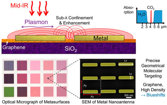
Figure 1.
Scanning electron microscopy images of the fabricated metal metasurfaces patterned on SiO2 covered substrates. Metal thickness (50 nm), design width (200 nm), and nanogap distance (200 nm) were fixed, whilst the lateral pitch Py and horizontal metal lengths Lx were varied. From left to right, the density of metal antennas and coverage % are increased, whilst the horizontal metal lengths Lx were also slightly increased to compensate for Py-induced blueshifts and targeting CO2 (4.25 μm) with their peak photoresponse wavelengths.

Figure 2.
(a) Linear polarized micro-FTIR spectra of the fabricated metasurfaces shows two clear mid-infrared photoresponses peaks, λ1, λ2. Here, the metasurface photoresponses λ1 were targeted at the 4.25 μm absorption peak for CO2, with wavelength dependent peak interaction intensities increasing with the metal coverage. (b) Measured dependence of the peak-response wavelengths (λ1, λ2) on the designed metal length (Lx), for different array pitch (Py). λ1 can be attributed to the metal metasurface geometry and increases with metal length Lx whilst decreasing with sub-wavelength metal coverage densities (Pitch, %Metal). The dashed line follows the expected trend for isolated nanoantenna, derived in Section 3.3.

Figure 3.
(a) Example optoelectronic hybrid graphene metasurface device patterned on a monolayer CVD graphene—SiO2 substrate, imaged by LUT contrast enhanced optical microscopy during processing [44]. (b) Micro-FTIR reflectance comparing the different material related photoresponse of different hybrid graphene metasurface optoelectronic device areas, measured in ambient conditions. The figure inset shows a blueshifted photoresponse peak with the addition of graphene, as measured for the same geometrical metastructures.

Figure 4.
(a) Transmission coefficient of normal incident IR plane waves through a single graphene sheet. (b) Time-resolved transmission spectrum by FDTD shown in (c). (d) The x-component of the transmitting electromagnetic field (black line: Ex through the graphene sheet; red line: transmission without the graphene sheet).

Figure 5.
FDTD transmittance spectra of parallel (Ex, Hy) polarized EM fields. The gold metasurface geometry was Lx × Ly × Lz = 1.4 × 0.2 × 0.05 μm3, with pitch Px × Py = 1.6 × 1.2 μm2. The number of simulation steps was increased from (a) 4 × 10⁵, (b) 8 × 10⁵, up to (c) 16 × 105 to allow all transmitted EM field through the detector. The addition of graphene is associated with a blueshift in the photoresponse, in close agreement with experimental FTIR spectra (Table 1).

Figure 6.
Dependence of the peak-response wavelengths on the metal length Lx and lateral pitch Py. Strong blueshifts are evident for Py < λ1, and where the gold metasurfaces are integrated with graphene. Analysis of these trends enables simple and effective targeted design of the metasurface geometries.


Table 1.
Graphene-induced blueshifts in the FTIR peak photoresponses of metasurface arrays following transfer of monolayer CVD graphene (G).
Table 1.
Graphene-induced blueshifts in the FTIR peak photoresponses of metasurface arrays following transfer of monolayer CVD graphene (G).
| Identification | Metal Geometry, μm | Peak Photoresponse Wavelengths, μm | |||||||||
|---|---|---|---|---|---|---|---|---|---|---|---|
| Sample | Position | Px | Py | Lx | Ly | λ1 | λ1 (+G) | ∆λ1 (G) | λ2 | Λ2 (+G) | ∆λ2 (G) |
| FDTD | Simulation | 1.60 | 1.2 | 1.4 | 0.2 | 4.10 | 3.63 | −0.47 | - | - | - |
| G1 | A | 1.40 | 2.5 | 1.18 | 0.24 | 4.02 | 3.81 | −0.21 | 9.71 | 9.30 | −0.41 |
| G1 | B | 1.30 | 5.0 | 1.18 | 0.24 | 4.26 | 3.94 | −0.32 | 9.78 | 9.40 | −0.38 |
| G2 | A | 1.65 | 5.0 | 1.54 | 0.30 | 5.10 | 4.72 | −0.38 | 9.90 | 9.75 | −0.15 |
| G2 | B | 1.65 | 5.0 | 1.53 | 0.31 | 5.45 | 4.75 | −0.70 | 9.92 | 9.79 | −0.13 |
| G2 | C | 2.40 | 5.0 | 1.54 | 0.31 | 5.70 | 4.80 | −0.90 | 9.94 | 9.82 | −0.12 |
| Average | 4.91 | 4.40 | −0.50 | 9.85 | 9.61 | −0.24 | |||||
Table 2.
Estimated metal metasurface geometries for midinfrared molecular targeting, for a range of metal lengths Lx and lateral pitch Py, with and without the presence of graphene.
Table 2.
Estimated metal metasurface geometries for midinfrared molecular targeting, for a range of metal lengths Lx and lateral pitch Py, with and without the presence of graphene.
| CH4 | CO2 | N2O | CO | O3 | NO | |||
|---|---|---|---|---|---|---|---|---|
| Material | Py (μm) | δL (%) | Lx (μm) | |||||
| Au-SiO2 | 10 | 3 | 0.82 | 1.06 | 1.12 | 1.16 | 1.18 | 1.30 |
| 5 | 5 | 0.84 | 1.09 | 1.15 | 1.20 | 1.21 | 1.33 | |
| 2.5 | 10 | 0.89 | 1.15 | 1.22 | 1.26 | 1.28 | 1.41 | |
| 1.2 | 22 | 1.02 | 1.32 | 1.39 | 1.45 | 1.47 | 1.61 | |
| G-Au-SiO2 | 10 | 4 | 0.92 | 1.18 | 1.25 | 1.30 | 1.32 | 1.45 |
| 5 | 7 | 0.95 | 1.23 | 1.30 | 1.35 | 1.37 | 1.50 | |
| 2.5 | 14 | 1.03 | 1.33 | 1.41 | 1.46 | 1.48 | 1.63 | |
| 1.2 | 30 | 1.26 | 1.62 | 1.72 | 1.78 | 1.81 | 1.98 | |
| λ (μm) | 3.3 | 4.25 | 4.5 | 4.67 | 4.74 | 5.2 | ||
Disclaimer/Publisher’s Note: The statements, opinions and data contained in all publications are solely those of the individual author(s) and contributor(s) and not of MDPI and/or the editor(s). MDPI and/or the editor(s) disclaim responsibility for any injury to people or property resulting from any ideas, methods, instructions or products referred to in the content. |
© 2023 by the authors. Licensee MDPI, Basel, Switzerland. This article is an open access article distributed under the terms and conditions of the Creative Commons Attribution (CC BY) license (https://creativecommons.org/licenses/by/4.0/).
Share and Cite
MDPI and ACS Style
Yager, T.; Chikvaidze, G.; Wang, Q.; Fu, Y. Graphene Hybrid Metasurfaces for Mid-Infrared Molecular Sensors. Nanomaterials 2023, 13, 2113. https://0-doi-org.brum.beds.ac.uk/10.3390/nano13142113
AMA Style
Yager T, Chikvaidze G, Wang Q, Fu Y. Graphene Hybrid Metasurfaces for Mid-Infrared Molecular Sensors. Nanomaterials. 2023; 13(14):2113. https://0-doi-org.brum.beds.ac.uk/10.3390/nano13142113
Chicago/Turabian StyleYager, Tom, George Chikvaidze, Qin Wang, and Ying Fu. 2023. "Graphene Hybrid Metasurfaces for Mid-Infrared Molecular Sensors" Nanomaterials 13, no. 14: 2113. https://0-doi-org.brum.beds.ac.uk/10.3390/nano13142113
Note that from the first issue of 2016, this journal uses article numbers instead of page numbers. See further details here.